Article

Performance Optimization of CsPb(I1–xBrx)3 Inorganic Perovskite Solar Cells with Gradient Bandgap

1
Laboratory for Quantum Engineering and Micro-Nano Energy Technology, Faculty of Physics and Optoelectronic Engineering, Xiangtan University, Xiangtan 411105, China
2
Hunan Key Laboratory for Micro-Nano Energy Materials and Devices, Xiangtan University, Xiangtan 411105, China
3
College of Chemistry, Xiangtan University, Xiangtan 411105, China
*
Author to whom correspondence should be addressed.
Energies 2023, 16(10), 4135; https://doi.org/10.3390/en16104135
Submission received: 7 April 2023 / Revised: 11 May 2023 / Accepted: 12 May 2023 / Published: 17 May 2023
(This article belongs to the Collection Featured Papers in Solar Energy and Photovoltaic Systems Section)

Abstract

:
In recent years, inorganic perovskite solar cells (PSCs) based on CsPbI3 have made significant progress in stability compared to hybrid organic–inorganic PSCs by substituting the volatile organic component with Cs cations. However, the cubic perovskite structure of α-CsPbI3 changes to the orthorhombic non-perovskite phase at room temperature resulting in efficiency degradation. The partial substitution of an I ion with Br ion benefits for perovskite phase stability. Unfortunately, the substitution of Br ion would enlarge bandgap reducing the absorption spectrum range. To optimize the balance between band gap and stability, introducing and optimizing the spatial bandgap gradation configuration is an effective method to broaden the light absorption and benefit the perovskite phase stability. As the bandgap of the CsPb(I1–xBrx)3 perovskite layer can be adjusted by I-Br composition engineering, the performance of CsPb(I1–xBrx)3 based PSCs with three different spatial variation Br doping composition profiles were investigated. The effects of uniform doping and gradient doping on the performance of PSCs were investigated. The results show that bandgap (Eg) and electron affinity(χ) attributed to an appropriate energy band offset, have the most important effects on PSCs performance. With a positive conduction band offset (CBO) of 0.2 eV at the electron translate layer (ETL)/perovskite interface, and a positive valence band offset (VBO) of 0.24 eV at the hole translate layer (HTL)/perovskite interface, the highest power conversion efficiency (PCE) of 22.90% with open–circuit voltage (VOC) of 1.39 V, short–circuit current (JSC) of 20.22 mA/cm2 and filling factor (FF) of 81.61% was obtained in uniform doping CsPb(I1–xBrx)3 based PSCs with x = 0.09. By carrying out a further optimization of the uniform doping configuration, the evaluation of a single band gap gradation configuration was investigated. By introducing a back gradation of band gap directed towards the back contact, an optimized band offset (front interface CBO = 0.18 eV, back interface VBO = 0.15 eV) was obtained, increasing the efficiency to 23.03%. Finally, the double gradient doping structure was further evaluated. The highest PCE is 23.18% with VOC close to 1.44 V, JSC changes to 19.37 mA/cm2 and an FF of 83.31% was obtained.

1. Introduction

Organic–inorganic perovskite solar cells (PSCs) have simpler a manufacturing process, lower cost and higher theoretical efficiency than silicon-based solar cells [1]. They also have an excellent optical absorption capacity (>700 nm) [2], high absorption coefficients (104~105 cm−1) [3], high carrier mobility (>100 cm2V−1s−1) [4], long diffusion lengths (102~103 nm) [5] and low exciton binding energy (≈26 meV) [6]. Over the past decade, the efficiency of perovskite solar cells has increased from 3.9% to 25.73% [7,8], but the photo-instability and thermal instability of organic–inorganic perovskite solar cells have also restricted the commercialization of perovskite solar cells [9,10,11,12].
In recent years, cesium-based perovskite solar cells have attracted extensive attention because of their inorganic stability and outstanding light absorption capacity [13,14,15,16]. Inorganic halogen perovskite solar cells CsPbX3 (X = Cl, Br, I) have high thermal stability [17,18], and the highest efficiency of inorganic halogen perovskite solar cells based on CsPbI3 has reached 21.14% [19]. However, the black phase of the cubic perovskite structure α-CsPbI3, whose bandgap (Eg) is 1.68 eV, is unstable at room temperature because of the small tolerance factor [20]. It converts to a non-perovskite phase of δ-CsPbI3 (Eg = 2.8 eV), which is an indirect band gap semiconductor [14,21], resulting in a weakened optical absorption capacity. By incorporating an appropriate Br element concentration into CsPbI3 to form CsPb(I1–xBrx)3, the tolerance factor can be effectively improved, reducing the α-CsPbI3 formation temperature and the defect formation which can effectively inhibit non-radiative recombination to improve open–circuit voltage [22,23].
As CsPb(I1–xBrx)3 PSCs can obtain a suitable bandgap by adjusting the I–Br ratio to achieve spectral response conditions and can be better combined with solar cells of other materials, inorganic perovskite is one of the candidate materials for tandem solar cells. In recent years, further improving the conversion efficiency of inorganic perovskite tandem solar cells has been an important research topic. At present, CsPb(I1–xBrx)3 all–inorganic PSCs as the bottom cell of the layered solar cell have an efficiency of 23.21% [24], higher than the efficiency of single all–inorganic PSCs. The maximum efficiency of single-junction CsPb(I1–xBrx)3 PSCs can reach 21.14% [19]. The maximum efficiencies of CsPbI2Br, CsPbIBr2, and CsPbBr3 are 17.8% [25], 12.05% [26] and 11.08% [27], respectively. With the increase in Br content, the efficiency of all–inorganic PSCs continuously decreases. Because Eg increases and larger energy band offset with the increase of Br content lead to a decrease in the optical absorption range.
The advantage of the gradient bandgap structure is that it can optimize the interface energy offset. The gradient bandgap structure can be used to set different doping concentrations on both sides of the material, ensuring that each interface can obtain a better energy band alignment. At the same time, a built-in electric field can be formed within the absorption layer. The appropriate direction of the built-in electric field can promote the transfer of carriers, further improving the efficiency of PSCs. To further optimize the performance of CsPb(I1–xBrx)3 PSCs, we attempt to introduce a gradient bandgap structure into CsPb(I1–xBrx)3 PSCs to optimize the energy band and improve the open–circuit voltage.
In addition, while the organic hole transport layer can enable high efficiency in devices, the organic hole transport material (HTM) is prone to decomposition and typically requires additives (such as bistrifluoromethanesulfonimide lithium salt (LiTFSI) and Tributyl phosphate (TBP)) to assist, which can exacerbate device instability [28]. Therefore, this article first attempts to optimize the organic hole transport layer (HTL) by selecting a suitable HTM to improve device stability and reduce costs. Secondly, the influence of parameters of the uniform doping absorption layer on the performance of PSCs is analyzed. Finally, the gradient bandgap CsPb(I1–xBrx)3 PSCs are established to optimize the cell performance.

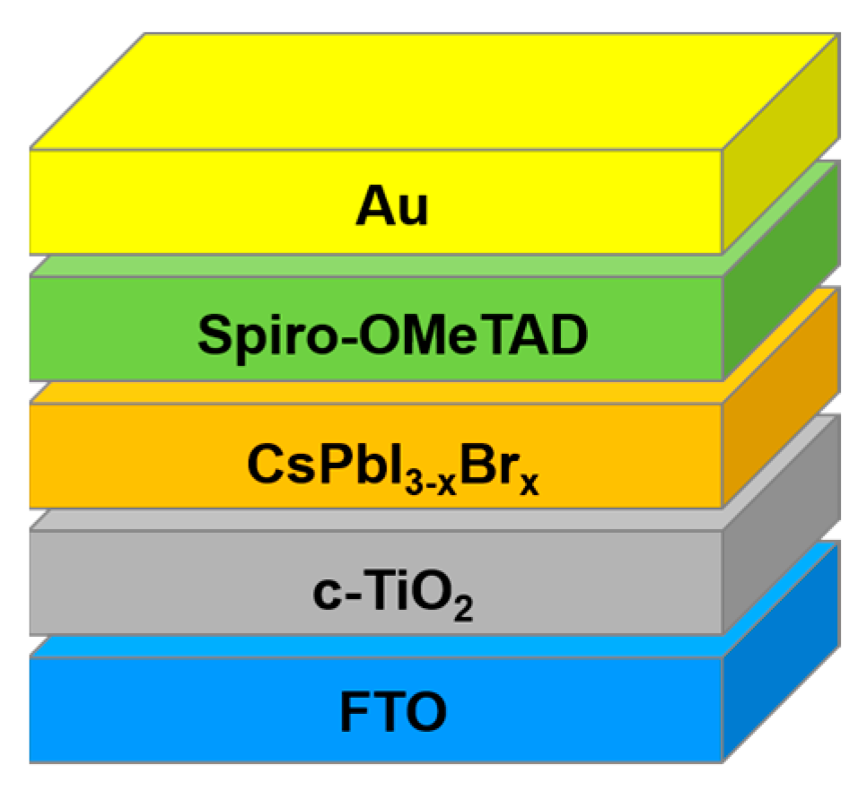
2. Device Simulation

The schematic structure of the simulated perovskite solar cell in this study is illustrated in Figure 1 as Au/Spiro-OMeTAD/CsPbI3/TiO2/FTO using SCAPS which is a one dimensional solar cell simulation program developed by the University of Gent, Belgium. The thickness of each layer material is as follows: 170 nm 2,2′,7,7′-Tetrakis [N,N-di(4-methoxyphenyl)amino]-9,9′-spirobifluorene(Spiro-OMeTAD), 750 nm CsPbI3, 25 nm compact-titanium dioxide (c-TiO2) and 300 nm fluorine-doped tin oxide (FTO). In detail, Au was used as a back contact, Spiro-OMeTAD as a p-type hole transport layer. CsPbI3 as a p-type absorber layer and c-TiO2 as an n-type buffer layer. FTO, as the front contact electrode, is a type of fluorine-doped SnO2 transparent conductive glass. Considering the interface recombination, two interface defect layers (IDLs) between the HTL/absorber layer and the electron transfer layer (ETL)/absorber layer, named IDL1 and IDL2, were considered in the simulated device. The Lambert Beer model was chosen as the optical model. Standard AM1.5G was used for incident spectrum. The incident light entered from the FTO side. Under illumination, we can calculate the open–circuit voltage (VOC), short–circuit current (JSC), fill factor (FF), power conversion efficiency (PCE) and other parameters, such as the current–voltage (J-V) characteristic curve and spectral response.
Table 1 shows the main parameters of the materials in the model [29,30,31,32,33,34,35,36]. The series resistance and shunt resistances were set to 3 Ωcm2 and 2150 Ωcm2, respectively. The electron and hole thermal velocities in each layer were set to 107 cm/s. The optical absorption coefficient (α) curve can be calculated by the equation α = Aα (hν·Eg)1/2, where Aα = 105. Apart from IDL1 and IDL2 having higher defect concentrations (Nt = 1015 cm−1), the other parameters of IDL1 and IDL2 were consistent with the absorption layer. The defect type was neutral. The defect distribution type of the absorption layer was Gaussian distribution. The defect distribution type of the other layers was single. The variation of each parameter in the absorbing layer is dependent on the value of x in CsPb(I1–xBrx)3. The linear law is shown below, where the parameters of CsPbI3, CsPbBr3 and CsPb(I1–xBrx)3 were assumed to be PI, PBr and Pdiop, respectively:
P d i o p = P I ( 1 x ) + P B r
The logarithmic law is shown below:
P d i o p = P I ( 1 x ) × P B r x
The simulated perovskite solar cell structure is based on the experimental literature of Yuqi Cui et al. [19]. In order to confirm the reliability of the device parameters used in this work, the simulated J-V characteristic were compared to the experimental result of the perovskite solar cell reported in reference [19] firstly. Figure 2 shows the simulated result comparing to the experimental data. The results of the J-V characteristic curve are similar to the result reported in the experimental literature [19] with VOC = 1.25 V, JSC = 21.61 mA/cm2, FF = 78.13%, and PCE = 21.18%., indicating that the simulation parameters used in this paper are valid.

3. Results and Discussion

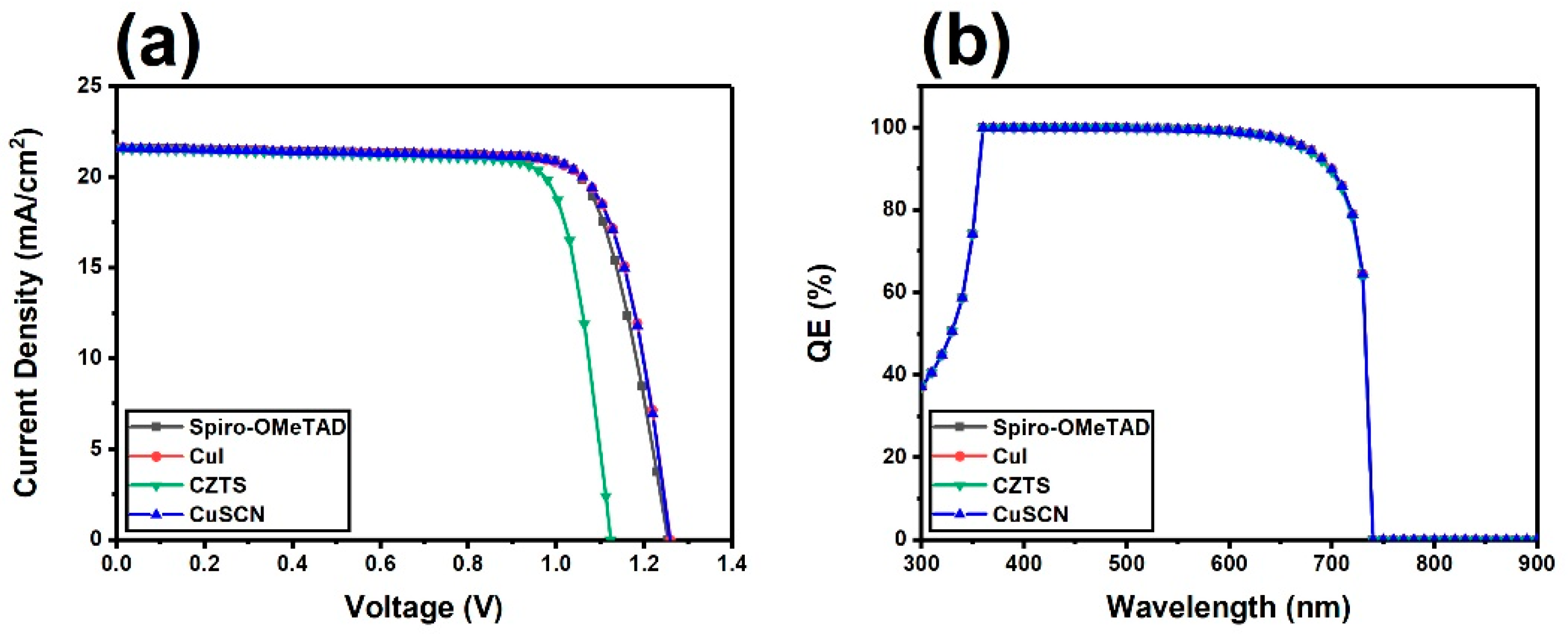
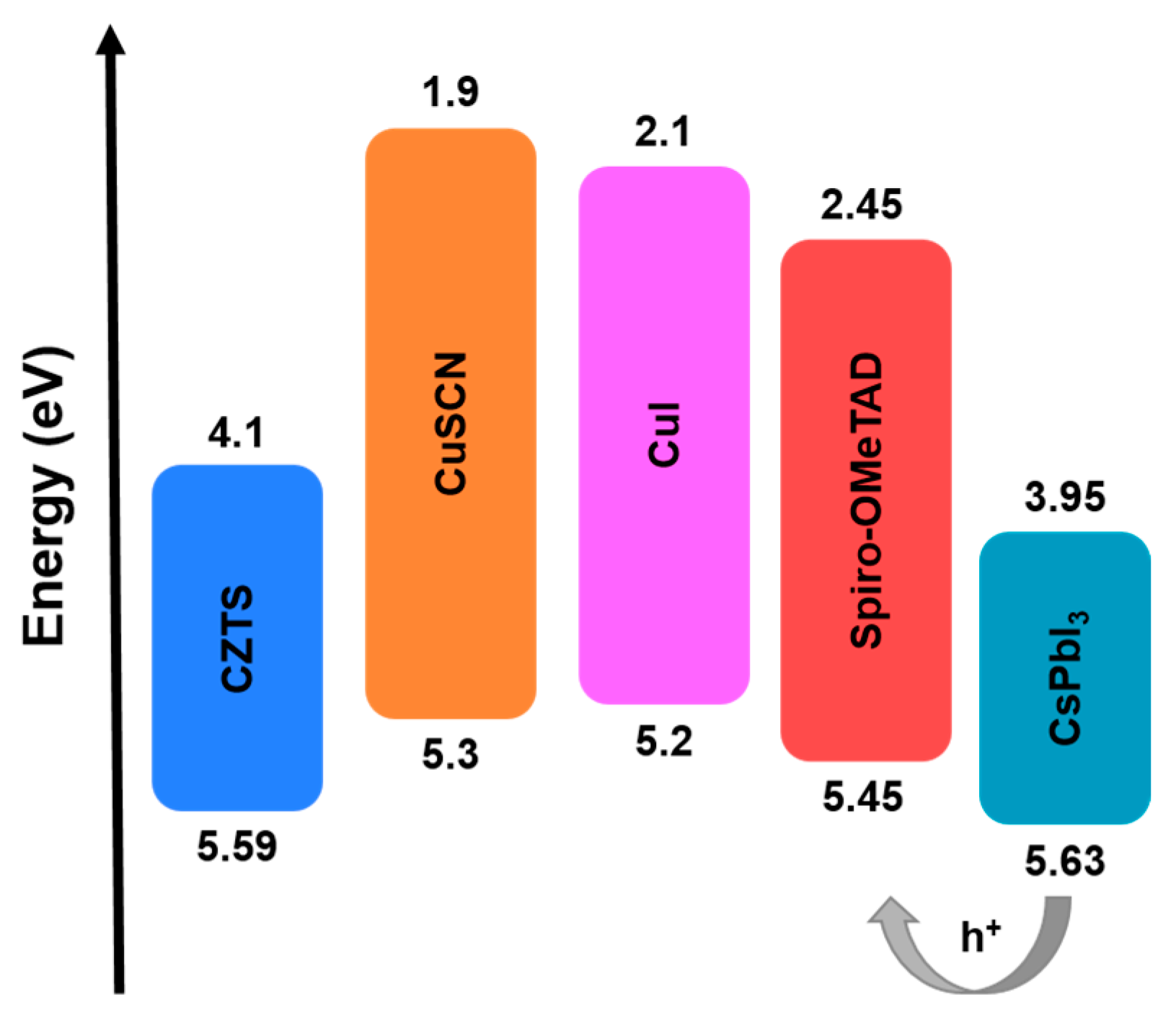
3.1. Influence of the Hole Transport Layer on Device Performance

In this section, we compare several commonly used inorganic HTMs and attempt to replace Spiro-OMeTAD. The material parameters used in this section are shown in Table 2 [37,38,39,40]. Figure 3 shows the J-V curves and quantum efficiency (QE) of different HTMs. Meanwhile, the computational results of various materials are shown in Table 3. By comparison, we can find that different HTMs have little effect on QE. This is because HTL is located on the back of the solar cell, so HTL has a relatively small impact on light absorption. The energy band plot (Figure 4) shows a good band arrangement between the valence band of the CsPbI3 and the highest occupied molecular orbital (HOMO) of all hole transport materials. By comparison, we can see that CZTS has the lowest VOC (1.12 eV), which is due to the narrow bandgap of CZTS. Therefore, CZTS is not an ideal material for CsPb(I1–xBrx)3 PSCs. Spiro-OMeTAD, CuI, and CuSCN exhibit similar efficiencies (21.18%, 21.22% and 21.25%, respectively). Although Spiro-OMeTAD and CuSCN have better band alignment than CuI, both of them have the drawbacks of being expensive and having low conductivity. Meanwhile, serious mutual diffusion between CuSCN and the absorber layer restricts the further performance improvement of the device [41]. CuI has better conductivity, higher carrier mobility and lower cost, so in the following work, CuI will replace Spiro-OMeTAD as the HTM.

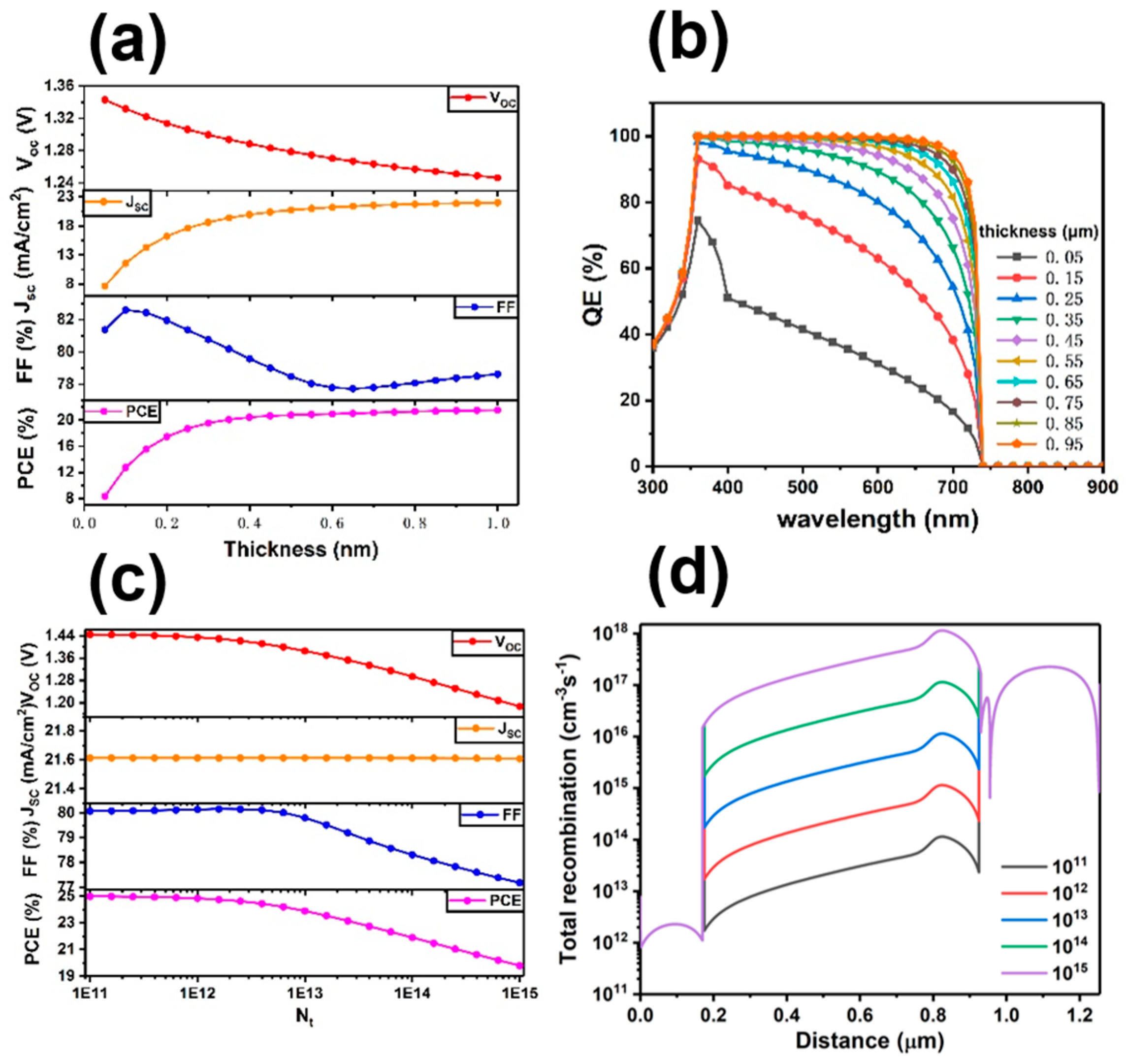
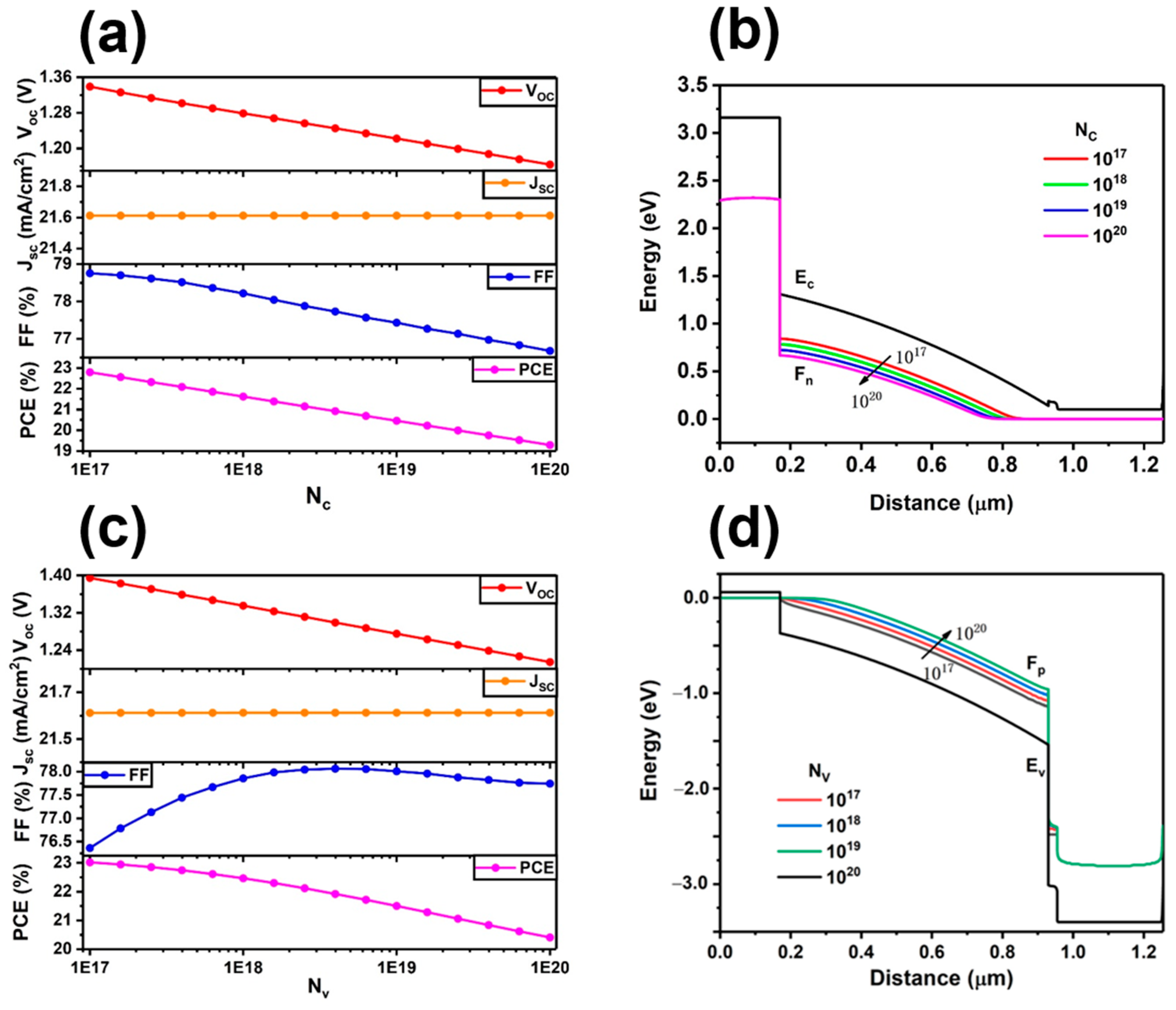
3.2. Influence of CsPbI3 Perovskite Layer Parameters on Device Performance

For the CsPbI3 absorption layer, the band gap (Eg), electron affinity (χ), dielectric constant (εr), conduction band effective density of states (NC), valence band effective density of states (NV), electron mobility (μn), hole mobility (μp), defect density (Nt) and other parameters of the material will change after doping with the Br element, and the influence of these parameters on the device performance is also different. Therefore, this section simulates the influence of each parameter on the device performance.
Figure 5 illustrates the relationship between device performance and various parameters, including thickness, NC, NV and Nt. As shown in Figure 5a,b, JSC increases with increasing thickness. The reason is that the absorbing layer can capture more photons, generating more electron–hole pairs, and increasing JSC. However, this also increases the series resistance and internal energy consumption, leading to a decrease in VOC and FF. When the thickness is too high, the device efficiency growth slows down. The reason is that the series resistance will further increase and more carrier recombination will occur, resulting in an increase in the recombination current. This also explains why JSC increases slowly. Moreover, too thick an absorbing layer will increase manufacturing costs, so the thickness should be controlled within approximately 750 nm. As shown in Figure 5c,d, an excessive doping concentration can lead to more charge carriers being trapped by defects, resulting in a decrease in VOC with increasing doping concentration. Due to the increase in doping concentration, scattering and recombination increase, suppressing hole transport. Therefore, selecting an appropriate doping concentration can improve the performance of the cell. Considering the increase in cost caused by too low doping, Nt should be kept within 1014 cm−3 in industrial production.
As shown in Figure 6a,b, with an increase in NC, the Fermi level decreases, which leads to a reduction in the built-in electric field within the absorption layer. This reduction is detrimental to the separation of charge carriers at the interface, resulting in an increase in recombination current and a decrease in VOC. As shown in Figure 6c,d, NV has a similar effect on cell performance to NC. With an increase in NV density, the Fermi level rises, which leads to a reduction in the built-in electric field within the absorption layer. This reduction is detrimental to the separation of charge carriers at the interface, resulting in an increase in recombination current and a decrease in VOC.
In addition to the above parameters, Eg and χ have a more significant impact on PSCs performance. Figure 7 shows the effect of Eg and χ on PSCs performance. The maximum PCE is 22.12% when Eg is 1.68 eV and χ is 3.78 eV. However, not every pair of Eg -χ data can be implemented in experiment. There is a fixed correspondence between them. Therefore, such high-efficiency doping cannot be achieved in the experiment. As shown in Figure 7, the increase in Eg leads to the increase in VOC. At the same time, because the wider bandgap is not conducive to the light absorption (Figure 8a), the photon-generated carrier will be greatly reduced, resulting in a sharp decline in JSC, and thus the reduction of cell efficiency. The change of Eg and χ will lead to band offset, which is another cause of PSCs performance change (Figure 8b). Take the valence band as an example, when Eg = 1.68 eV and χ = 3.4 eV, the valence band of HTL is lower than the absorption layer and a “spike” will be formed at the interface. When Eg =1.68 eV and χ =3.8 eV, the valence band of the hole layer is higher than that of the absorption layer, and a “cliff” will be formed at the interface. Excessive band offset will hinder carrier diffusion and lead to the incomplete depletion of the absorption layer. The carrier cannot be collected during its lifetime, leading to the increase in carrier recombination rate. Therefore, suitable Eg and χ can optimize the energy band at the interface and improve the PSCs’ efficiency.

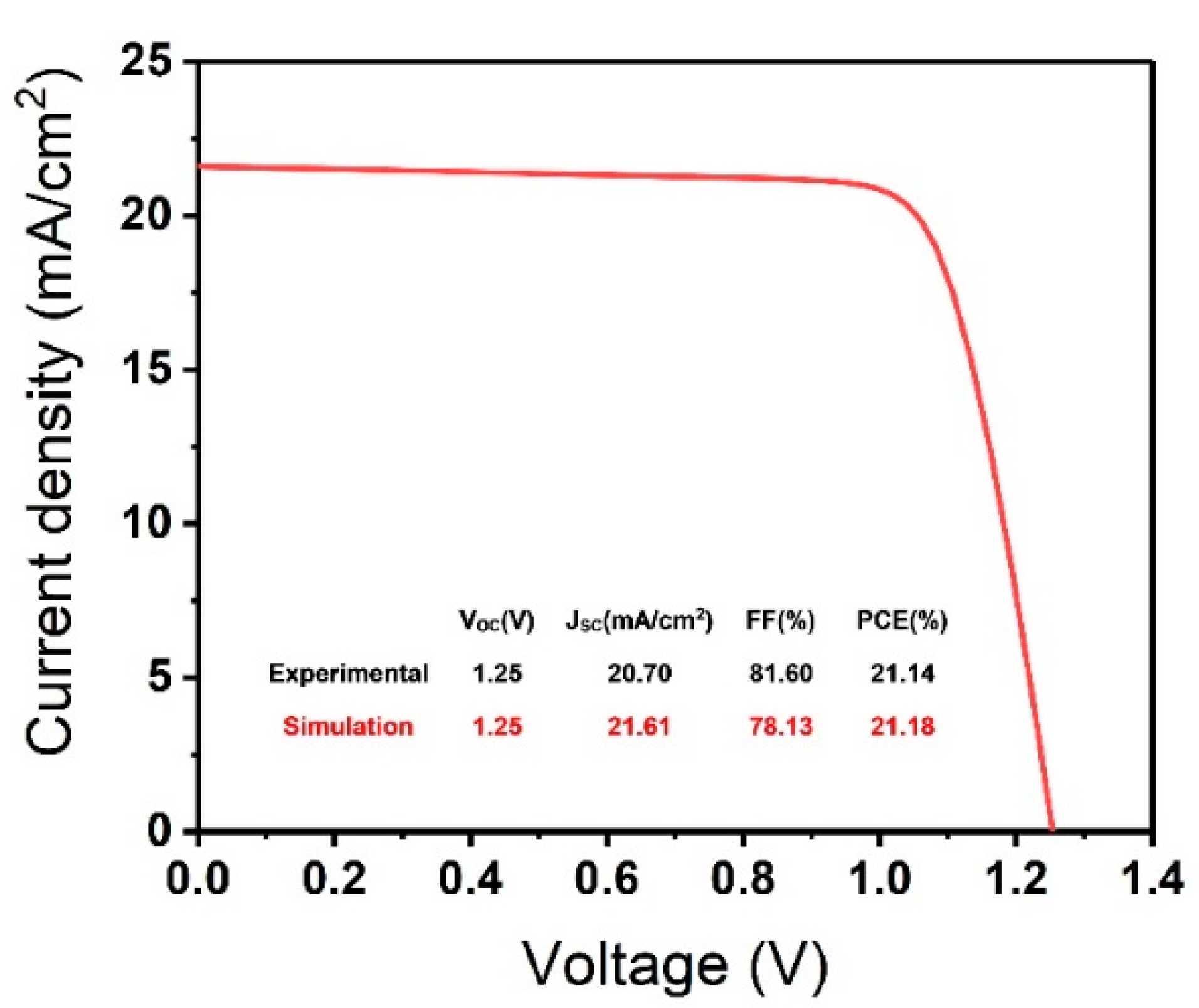
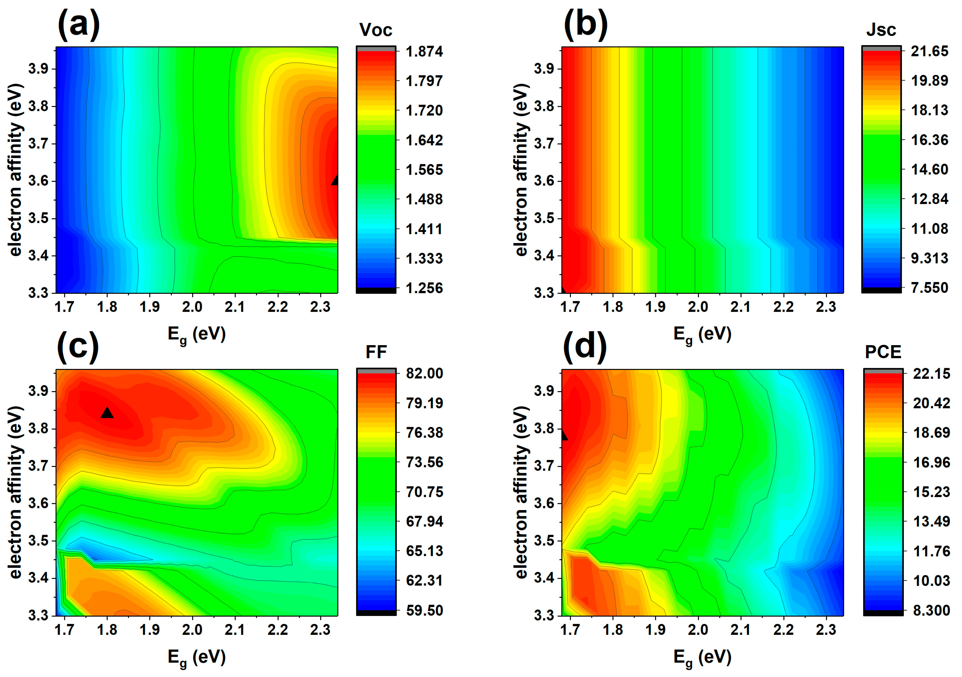
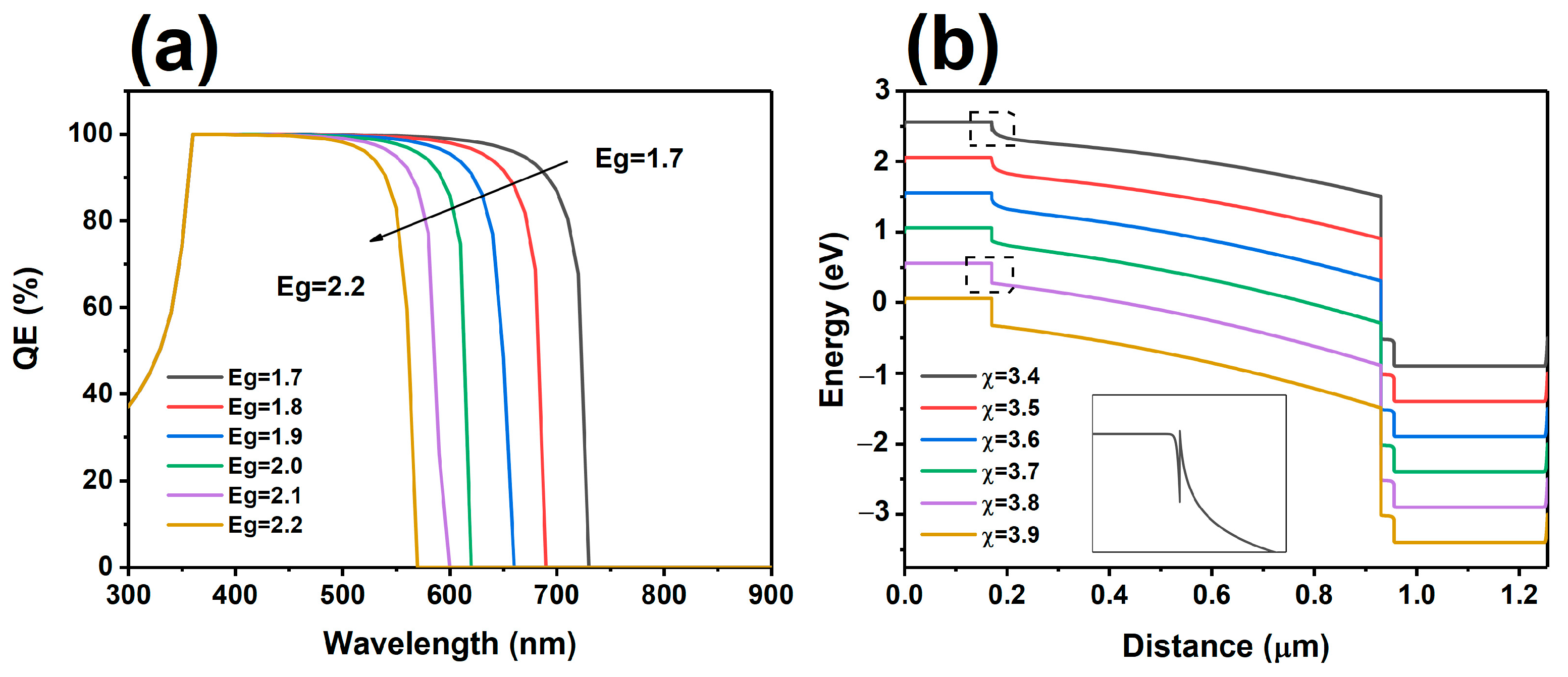
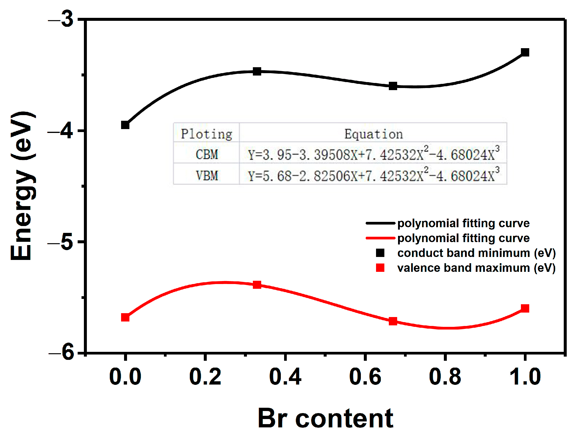
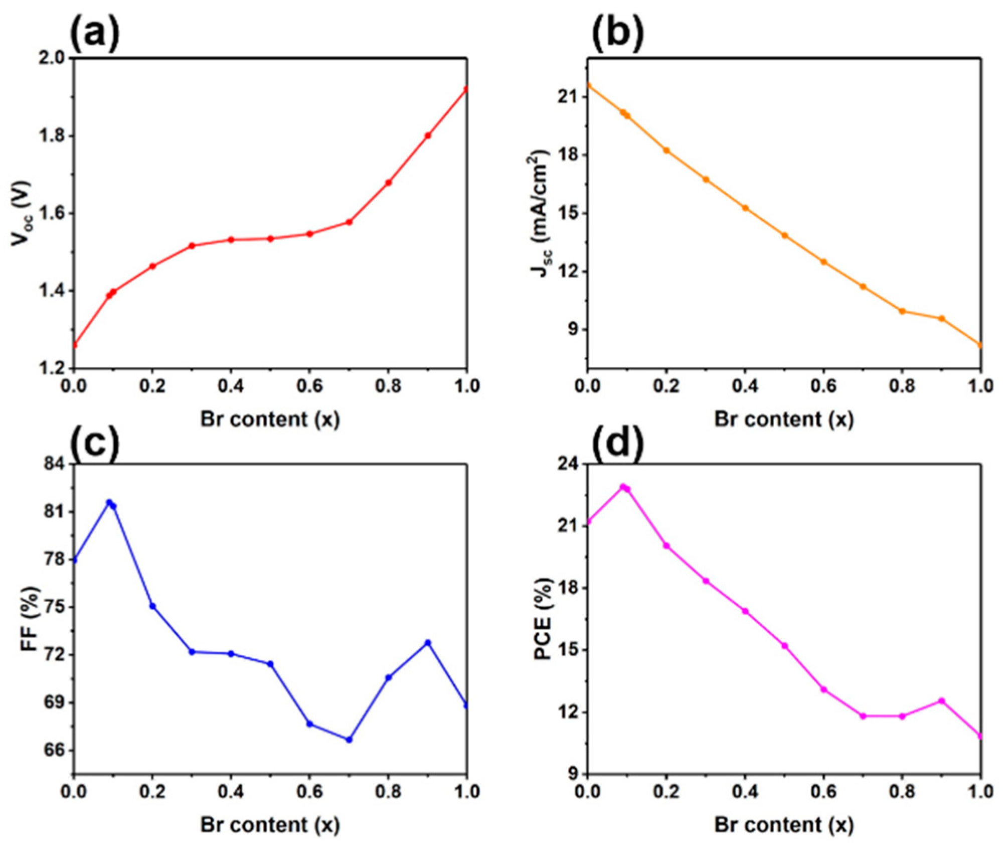
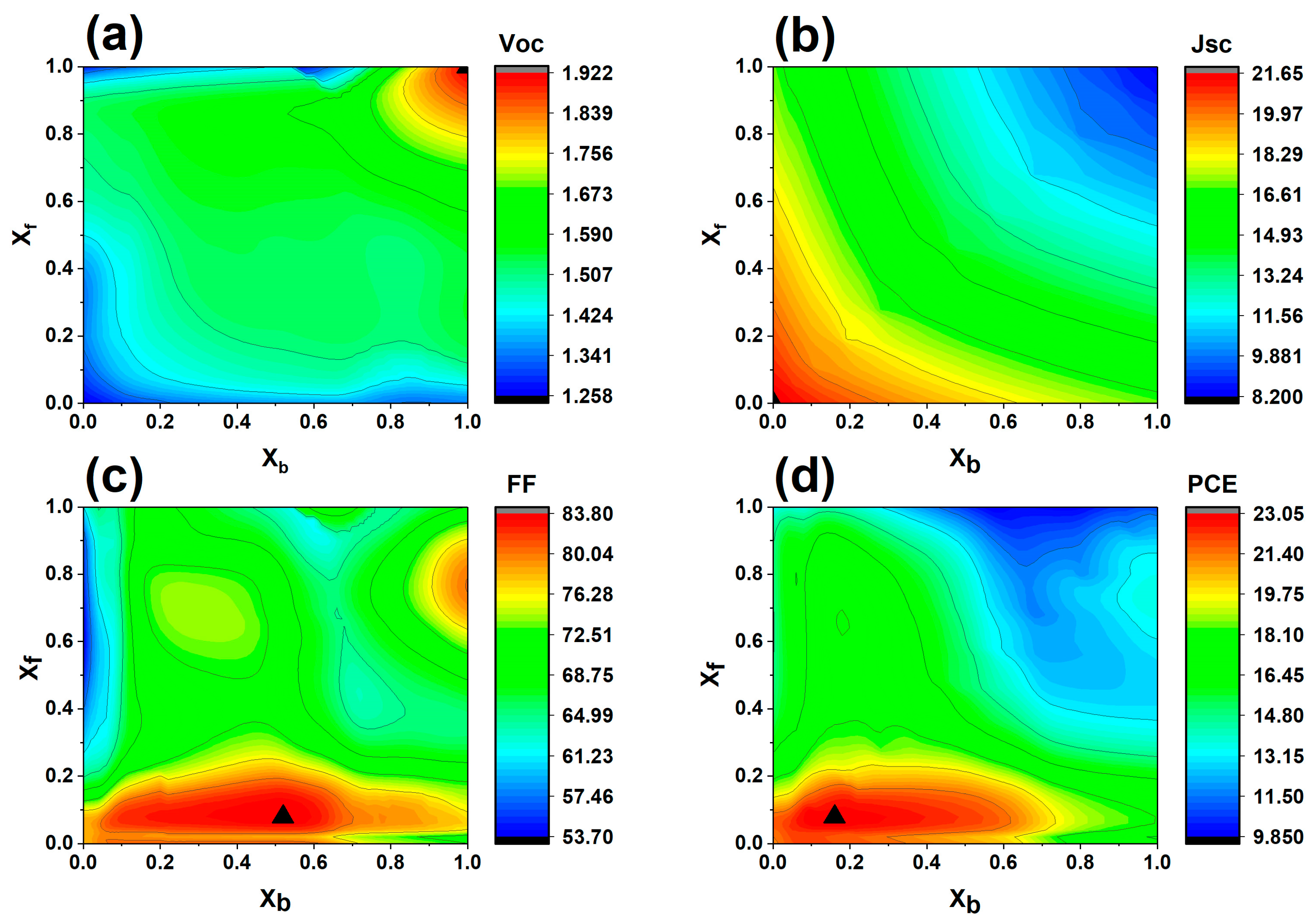
3.3. Uniform Composition Configuration

The energy band of the absorption layer CsPb(I1–xBrx)3 is closely related to the x value. According to the experimental results of Yuanzhi Jiang et al. [42], the variation curves of the conduction and valence bands of CsPb(I1–xBrx)3 with x value can be obtained by polynomial fitting (Figure 9) [42,43,44,45]. It can be seen from Figure 9 that with the increase in Br content, both the bottom of the conduction band and the top of the valence band first increase and then decrease before increasing again, but Eg keeps increasing. The relationship between x values in the CsPb(I1–xBrx)3 absorption layer in this model and other parameters (energy band, εr, NC, NV, μn and μp) has been shown in Table 1. As shown in Figure 10, the effect of Br content change on the performance of CsPb(I1–xBrx)3 PSCs is simulated here. The results show that when x = 0, the efficiency of CsPb(I1–xBrx)3 perovskite solar cells reaches 21.22%, VOC is 1.26 V, JSC is 21.26 mA/cm2 and FF is 77.94%. When the x value gradually increases, the efficiency increases first, and reaches the maximum when x = 0.09, VOC = 1.39 V, JSC = 20.22 mA/cm2, FF = 81.61% and PCE = 22.9%, and then the efficiency starts to diminish. One reason is that an excessive energy band results in a reduced light absorption range, which in turn leads to a decrease in JSC (Figure 11).
The other reason is that when x = 0.09, the valence band offset (VBO) is 0.24 eV (Figure 12a), and the conduction band offset (CBO) is 0.2 eV (Figure 12b). The band offset is significantly better than x = 0.25, 0.5, 0.75 and 1. Compared with x = 0, although CBO (−0.05 eV) increased, VBO (0.43 eV) decreased significantly. This makes the band offset close to a reasonable range of 0–0.2 eV [46]. Therefore, the band matching is better when x = 0.09, effectively reducing the carrier recombination rate inside the cell (Figure 12c), and the PSCs efficiency reaches the maximum.

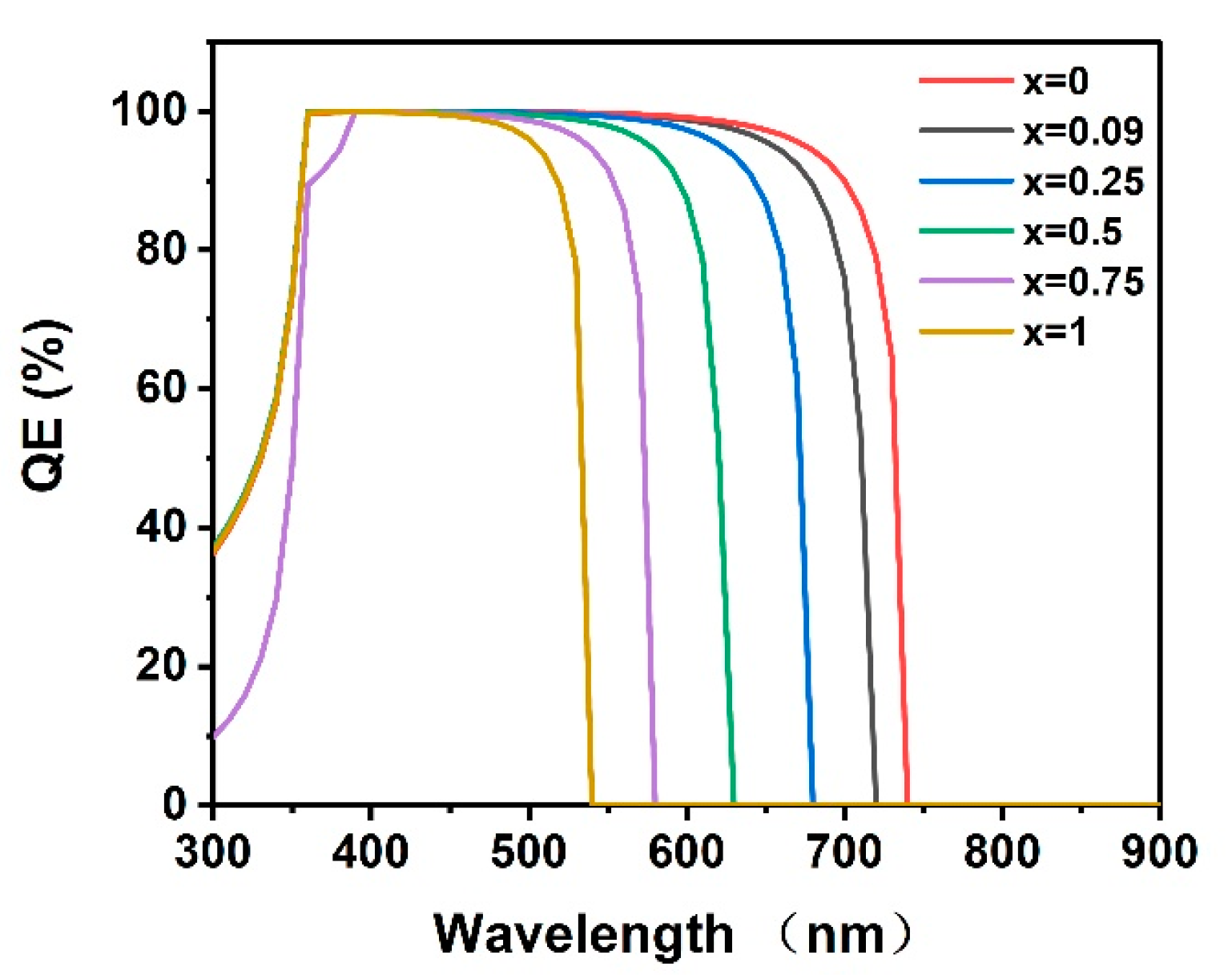
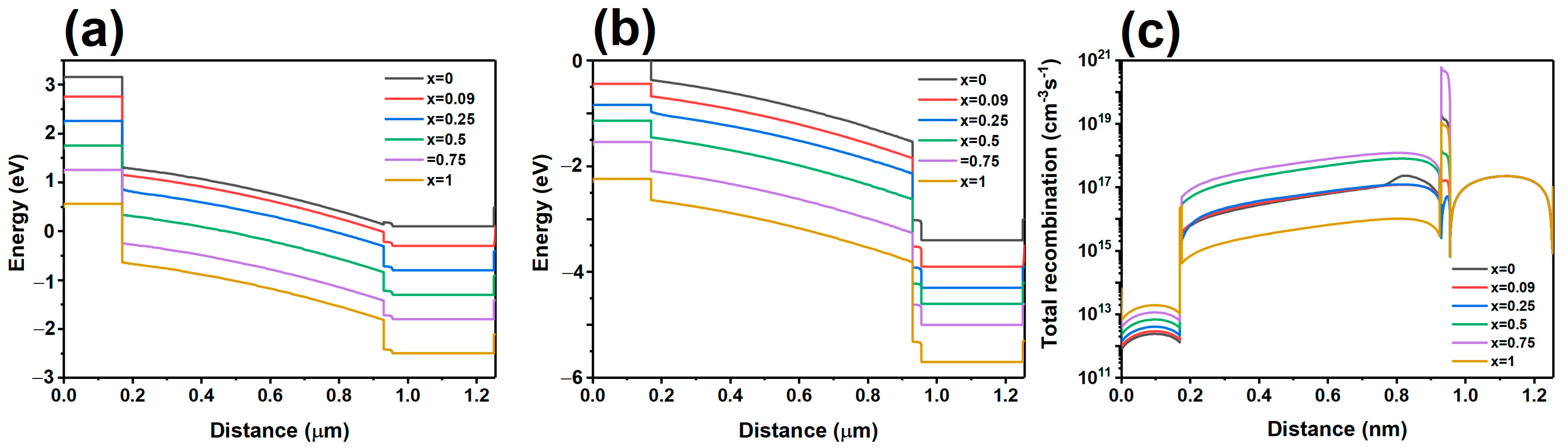
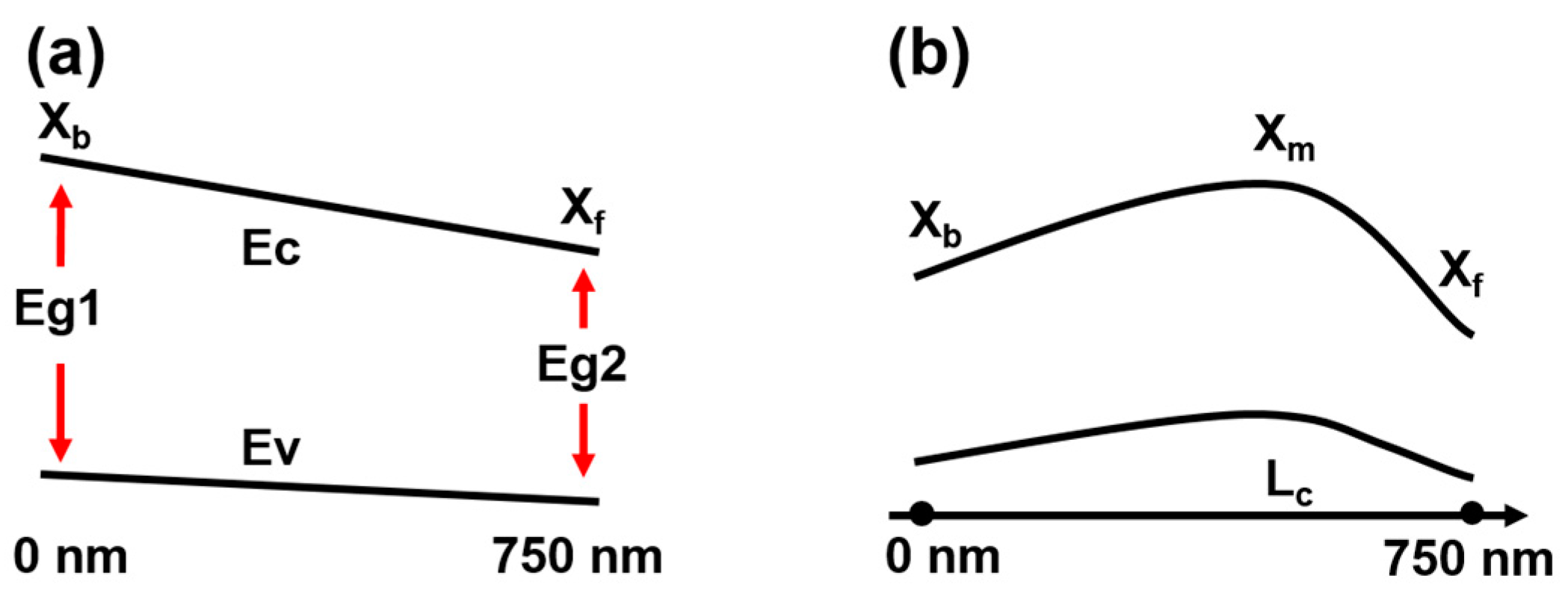
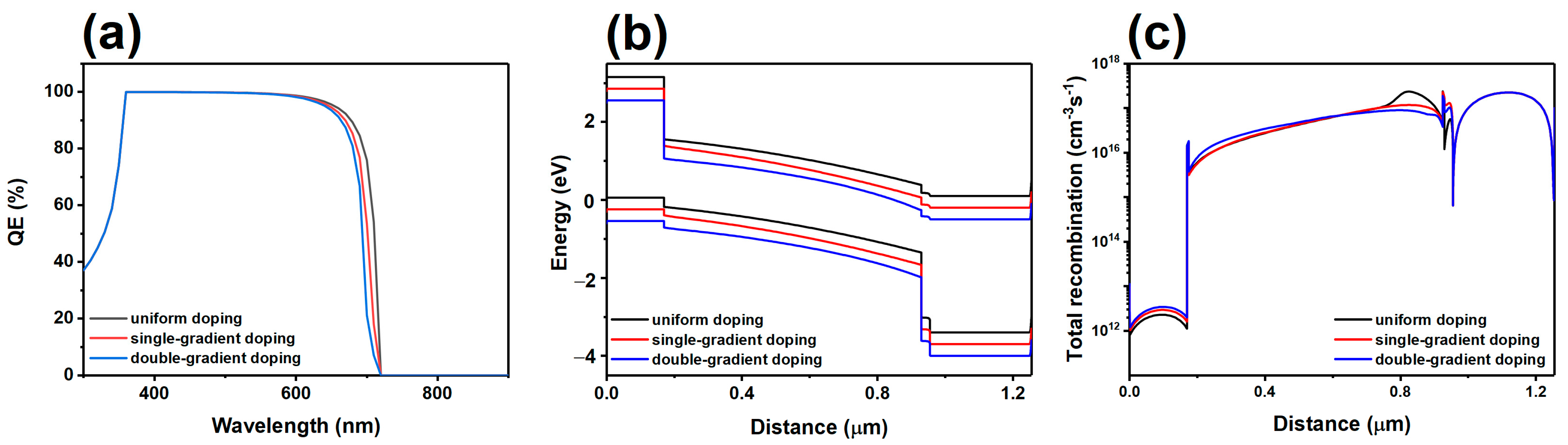
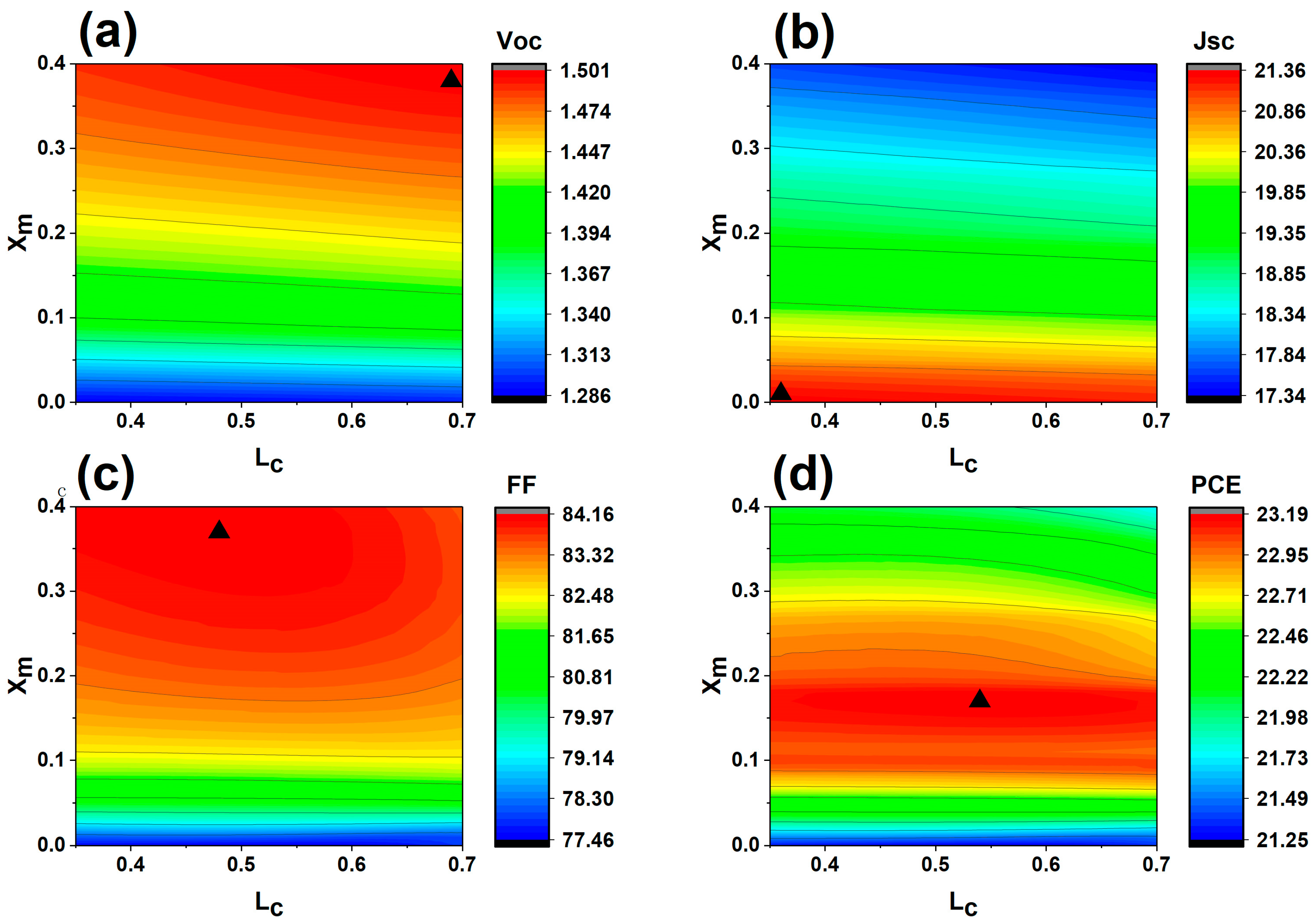
3.4. Gradient Composition Configuration

Gradient doping can effectively improve the photoelectric conversion efficiency of perovskite solar cells. Therefore, a similar doping method is applied to CsPb(I1–xBrx)3 perovskite solar cells in this study. Figure 13 shows two different types of gradient doping. The Br doping density of the CsPb(I1–xBrx)3 absorption layer is controlled by the depth. The x value changes linearly with the depth, so that the energy band changes accordingly. The Eg increases with the increase in the x value, when the Br content of the absorption layer/ETL (Xf) is higher than the Br content of the absorption layer/HTL (Xb). This is called the pre-segregation structure; otherwise, it is called the post-segregation structure.
When Xb is unchanged, the cell performance will gradually decay with the increase in Xf. This is because with the increase in Xf, the band gap of the absorption layer at the CsPb(I1–xBrx)3/ETL interface gradually increases, forming a pre-segregation structure, thus generating a built-in electric field in the absorption layer in the opposite direction, which is not conducive to the collection of carriers and aggravates the recombination of carriers. An increase in the reverse saturation current leads to a decrease in the conversion efficiency.
The black icon marked in Figure 14 is the position corresponding to the simulated optimal cell efficiency. When Xb = 0.17 and Xf = 0.08, the cell performance reaches its best, and VOC is 1.39 V, JSC is 20.22 mA/cm2, FF is 82.12%, and PCE is 23.03%. At this time, the bandgap of the rear interface Eg1 = 1.79 eV, and the bandgap of the front interface Eg2 = 1.73 eV. The conduction band and valence band gradually rise from the front interface to the back interface, forming a post-segregation structure. A built-in electric field in the same direction is formed within the absorption layer, which enhances carrier separation, promotes carrier collection and reduces recombination, thus improving cell performance. Compared with uniform doping, QE decreases in single gradient doping (Figure 15a), which is because the increase in Eg makes carrier separation more difficult and reduces the light absorption capacity. Figure 15b shows the energy band after translation, and we calculated that the CBO of single gradient doping is 0.18 eV, and VBO is 0.15 eV. The CBO of uniform doping is 0.2 eV and VBO is 0.24 eV. The smaller band offset leads to a decrease in the carrier recombination rate (Figure 15c).
Jiang Jie et al. proposed a double-gradient doping structure to optimize cell performance [47]. This kind of band structure is concave, high on both sides and low in the middle, which can improve JSC. This structure is applied to the CsPb(I1–xBrx)3 absorption layer (Figure 13b). A more appropriate band gap near the front surface of the absorption layer can improve carrier transfer efficiency. Xf, Xb, LC and Xm represent the Br doping concentration on the front surface, the Br doping concentration on the back surface, the doping depth, and the maximum or minimum Br doping concentration inside the absorption layer, respectively. The impact of Xb and Xf on PSCs’ performance has been discussed previously. Figure 16 shows the effect of LC and Xm on PSCs performance. When Xf = 0.07, Xb = 0.15, LC = 600 nm and Xm = 0.17, PSCs performance reaches its highest (VOC = 1.44 V, JSC = 19.37 mA/cm2, FF = 83.31% and PCE = 23.18%).
Comparing single-gradient doping with double-gradient doping, QE decreases slightly because the energy band is slightly larger (Figure 15a). The best efficiency of double-gradient doping is 0.15% higher than that of single-gradient doping. The improvement mainly focuses on the increase in VOC by 0.05 eV, the decrease in JSC by 0.85 mA/cm2 and the increase in FF by 1.19%. This is contrary to the experimental results of Jiang Jie et al. One reason is that the sunlight is incident on the front interface, and the front interface concentrations of single-gradient doping and double-gradient doping are not much different, so the range of light absorption is almost constant. However, since the doping concentration of the absorption layer reaches the maximum (Xm = 0.17) when LC = 540 nm, LC is closer to the front interface (absorption layer/ETL), Eg = 1.79 eV. Xb = 0.15, Eg1 = 1.77 eV, Xf = 0.07, Eg2 = 1.72 eV. It can be seen that compared with single-gradient doping, the bandgap of double-gradient doping in the first half of the absorption layer (LC—front interface) increases faster, while the bandgap of the second half (LC—back interface) maintains a relatively high level. Previously, we analyzed that high bandgap would make it difficult for low-energy long-wavelength photons to be excited, so the absorption capacity of the absorption layer for long-wavelength light would be weakened (Figure 15a), and the number of electron–hole pairs generated would be reduced, thus leading to JSC weakening. Another reason is that in the second half, due to the difference in bandgap, an electric field will be formed in an opposite direction of the in-built electric field, which has a negative effect on the transmission of carriers. It can be seen from Figure 16 that when Xm <0.07 or Xm >0.25, the cell efficiency drops sharply. The reason may be that too small a band gap will form a built-in electric field near the front surface in the direction opposite to the built-in electric field in the absorption layer, which will increase the carrier recombination rate at the interface, while too large a band gap will reduce light absorption. The CBO and VBO of double gradient doping are 0.15 eV and 0.15 eV respectively (Figure 15a,b). The band offset is decreased on the front surface, so the carrier recombination rate on the front surface is reduced. VBO remains unchanged (Figure 15c). So, the energy band is optimized to improve the efficiency.

4. Conclusions

In this paper, a more accurate energy band variation plot of CsPb(I1–xBrx)3 PSCs was recovered, and SCAPS software was used to study and optimize the CsPb(I1–xBrx)3 perovskite solar cells with gradient bandgap. For the first time, we studied the effects of different HTM on PSCs performance, proving that a suitable HTL bandgap is important for PSCs performance, and selected CuI with a better carrier generation rate as the hole transport layer material. Second, we studied the influence of different parameters of the absorption layer on the PSCs performance. We find that the thickness of ~750nm can improve the optical absorption capacity while taking into account the efficiency and cost. Too large NC and NV will cause the Fermi level to move away from conduction band and valence band, resulting in VOC and efficiency loss. High Nt will lead to an increase in the carrier recombination rate, so Nt should be controlled within 1014 cm−3. Thirdly, the influence of uniform doping on PSCs performance was studied. We find that when x = 0.09, there is a better matched band at HTM/perovskite interface (VBO = 0.24 eV and CBO = 0.2 eV), with an efficiency of 22.90%. Finally, the influence of different types of gradient doping on PSCs performance was studied. Through the comparison, we find that although QE is slightly reduced by gradient doping, by adjusting the band, the band offset can be optimized (CBO = 0.18 eV, VBO = 0.15 eV), and a post-segregation structure can be formed to optimize carrier transport and increase efficiency (PCE = 23.03%). The energy band is further optimized by double–gradient doping (CBO = 0.10 eV, VBO = 0.15 eV), and the efficiency is increased to 23.18%.

Author Contributions

Conceptualization, S.Y. and L.W.; investigation, L.W. and T.X.; methodology, L.W. and S.Y.; software, L.W.; formal analysis, L.W.; validation, L.W. and Q.Y.; funding acquisition, S.Y., H.L. and J.Z.; project administration, S.Y.; resources, S.Y. and J.Y.; supervision, S.Y.; visualization, L.W. and S.Y.; writing—original draft, L.W.; writing—review and editing, S.Y. All authors have read and agreed to the published version of the manuscript.

Funding

This research was funded by the National Nature Science Foundation (grant numbers 51102203, 51772255, 11874316, 11474244), Hunan Provincial Natural Science Foundation of China (grant number 2016JJ3122) and Open Fund based on the Innovation Platform of Hunan Colleges and Universities (grant number 11K061).

Data Availability Statement

Not applicable.

Acknowledgments

The authors would like to acknowledge Marc Burgelman, University of Gent, Belgium, for providing the SCAPS solar cell simulation software.

Conflicts of Interest

The authors declare no conflict of interest.

References

  1. Zhaoyi, J.; Binkai, W.; Wenjun, Z.; Zhichun, Y.; Mengjie, L.; Fumeng, R.; Tahir, I.; Zhenxing, S.; Shasha, Z.; Yiqiang, Z.; et al. Solvent engineering towards scalable fabrication of high-quality perovskite films for efficient solar modules. J. Energy Chem. 2023, 80, 689–710. [Google Scholar]
  2. Li, Z.; Xu, J.; Zhou, S.; Zhang, B.; Liu, X.; Dai, S.; Yao, J. CsBr-Induced Stable CsPbI3–xBrx (x < 1) Perovskite Films at Low Temperature for Highly Efficient Planar Heterojunction Solar Cells. ACS Appl. Mater. Interfaces 2018, 10, 38183–38192. [Google Scholar]
  3. Sun, S.; Salim, T.; Mathews, N.; Duchamp, M.; Boothroyd, C.; Xing, G.; Sum, T.C.; Lam, Y.M. The origin of high efficiency in low-temperature solution-processable bilayer organometal halide hybrid solar cells. Energy Environ. Sci. 2014, 7, 399–407. [Google Scholar] [CrossRef]
  4. He, Y.; Galli, G. Perovskites for Solar Thermoelectric Applications: A First Principle Study of CH3NH3AI3 (A = Pb and Sn). Chem. Mater. 2014, 26, 5394–5400. [Google Scholar] [CrossRef]
  5. Yang, D.; Yang, R.; Zhang, J.; Yang, Z.; Liu, S.; Li, C. High efficiency flexible perovskite solar cells using superior low temperature TiO2. Energy Environ. Sci. 2015, 8, 3208–3214. [Google Scholar] [CrossRef]
  6. Ball, J.M.; Lee, M.M.; Hey, A.; Snaith, H.J. Low-temperature processed meso-superstructured to thin-film perovskite solar cells. Energy Environ. Sci. 2013, 6, 1739–1743. [Google Scholar] [CrossRef]
  7. Kojima, A.; Teshima, K.; Shirai, Y.; Miyasaka, T. Organometal Halide Perovskites as Visible-Light Sensitizers for Photovoltaic Cells. J. Am. Chem. Soc. 2009, 131, 6050–6051. [Google Scholar] [CrossRef] [PubMed]
  8. Park, J.; Kim, J.; Yun, H.S.; Paik, M.J.; Noh, E.; Mun, H.J.; Kim, M.G.; Shin, T.J.; Seok, S.I. Controlled growth of perovskite layers with volatile alkylammonium chlorides. Nature 2023, 616, 724–730. [Google Scholar] [CrossRef]
  9. Berhe, T.A.; Su, W.-N.; Chen, C.-H.; Pan, C.-J.; Cheng, J.-H.; Chen, H.-M.; Tsai, M.-C.; Chen, L.-Y.; Dubale, A.A.; Hwang, B.-J. Organometal halide perovskite solar cells: Degradation and stability. Energy Environ. Sci. 2016, 9, 323–356. [Google Scholar] [CrossRef]
  10. Salado, M.; Calio, L.; Berger, R.; Kazim, S.; Ahmad, S. Influence of the mixed organic cation ratio in lead iodide based perovskite on the performance of solar cells. Phys. Chem. Chem. Phys. 2016, 18, 27148–27157. [Google Scholar] [CrossRef] [PubMed]
  11. Han, Y.; Meyer, S.; Dkhissi, Y.; Weber, K.; Pringle, J.M.; Bach, U.; Spiccia, L.; Cheng, Y.-B. Degradation observations of encapsulated planar CH3NH3PbI3 perovskite solar cells at high temperatures and humidity. J. Mater. Chem. A 2015, 3, 8139–8147. [Google Scholar] [CrossRef]
  12. Service, R.F. Cesium fortifies next-generation solar cells. Science 2016, 351, 113–114. [Google Scholar] [CrossRef] [PubMed]
  13. Wang, K.; Jin, Z.; Liang, L.; Bian, H.; Bai, D.; Wang, H.; Zhang, J.; Wang, Q.; Liu, S. Publisher Correction: All-inorganic cesium lead iodide perovskite solar cells with stabilized efficiency beyond 15%. Nat. Commun. 2018, 9, 4935. [Google Scholar] [CrossRef] [PubMed]
  14. Eperon, G.E.; Paternò, G.M.; Sutton, R.J.; Zampetti, A.; Haghighirad, A.A.; Cacialli, F.; Snaith, H.J. Inorganic caesium lead iodide perovskite solar cells. J. Mater. Chem. A 2015, 3, 19688–19695. [Google Scholar] [CrossRef]
  15. Chen, Y.; Liu, X.; Wang, T.; Zhao, Y. Highly Stable Inorganic Lead Halide Perovskite toward Efficient Photovoltaics. Acc. Chem. Res. 2021, 54, 3452–3461. [Google Scholar] [CrossRef]
  16. Liang, J.; Liu, J.; Jin, Z. All-Inorganic Halide Perovskites for Optoelectronics: Progress and Prospects (Solar RRL 10/2017). Sol. RRL 2017, 1, 1770138. [Google Scholar] [CrossRef]
  17. Frolova, L.A.; Anokhin, D.V.; Piryazev, A.A.; Luchkin, S.Y.; Dremova, N.N.; Stevenson, K.J.; Troshin, P.A. Highly Efficient All-Inorganic Planar Heterojunction Perovskite Solar Cells Produced by Thermal Coevaporation of CsI and PbI2. J. Phys. Chem. Lett. 2017, 8, 67–72. [Google Scholar] [CrossRef] [PubMed]
  18. Sutton, R.J.; Eperon, G.E.; Miranda, L.; Parrott, E.S.; Kamino, B.A.; Patel, J.B.; Hörantner, M.T.; Johnston, M.B.; Haghighirad, A.A.; Moore, D.T.; et al. Bandgap-Tunable Cesium Lead Halide Perovskites with High Thermal Stability for Efficient Solar Cells. Adv. Energy Mater. 2016, 6, 1502458. [Google Scholar] [CrossRef]
  19. Cui, Y.; Shi, J.; Meng, F.; Yu, B.; Tan, S.; He, S.; Tan, C.; Li, Y.; Wu, H.; Luo, Y.; et al. A Versatile Molten-Salt Induction Strategy to Achieve Efficient CsPbI3 Perovskite Solar Cells with a High Open–Circuit Voltage > 1.2 V. Adv. Mater. 2022, 34, 2205028. [Google Scholar] [CrossRef] [PubMed]
  20. Li, Z.; Yang, M.; Park, J.-S.; Wei, S.-H.; Berry, J.J.; Zhu, K. Stabilizing Perovskite Structures by Tuning Tolerance Factor: Formation of Formamidinium and Cesium Lead Iodide Solid-State Alloys. Chem. Mater. 2016, 28, 284–292. [Google Scholar] [CrossRef]
  21. Sharma, S.; Weiden, N.; Weiss, A. Phase Diagrams of Quasibinary Systems of the Type: ABX3—A′BX3; ABX3—AB′X3, and ABX3—ABX′3; X = Halogen. Z. Phys. Chem. 1992, 175, 63–80. [Google Scholar] [CrossRef]
  22. Nam, J.K.; Chai, S.U.; Cha, W.; Choi, Y.J.; Kim, W.; Jung, M.S.; Kwon, J.; Kim, D.; Park, J.H. Potassium Incorporation for Enhanced Performance and Stability of Fully Inorganic Cesium Lead Halide Perovskite Solar Cells. Nano Lett. 2017, 17, 2028–2033. [Google Scholar] [CrossRef]
  23. Faheem, M.B.; Khan, B.; Feng, C.; Farooq, M.U.; Raziq, F.; Xiao, Y.; Li, Y. All-Inorganic Perovskite Solar Cells: Energetics, Key Challenges, and Strategies toward Commercialization. ACS Energy Lett. 2020, 5, 290–320. [Google Scholar] [CrossRef]
  24. Sun, S.-Q.; Xu, X.; Sun, Q.; Yao, Q.; Cai, Y.; Li, X.-Y.; Xu, Y.-L.; He, W.; Zhu, M.; Lv, X.; et al. All-Inorganic Perovskite-Based Monolithic Perovskite/Organic Tandem Solar Cells with 23.21% Efficiency by Dual-Interface Engineering. Adv. Energy Mater. 2023, 13, 2204347. [Google Scholar] [CrossRef]
  25. Yuanjia, D.; Qiang, G.; Yanfang, G.; Zheng, D.; Zhibin, W.; Zongwei, C.; Qing, G.; Zhi, Z.; Yongfang, L.; Erjun, Z. A low-cost hole transport layer enables CsPbI2Br single-junction and tandem perovskite solar cells with record efficiencies of 17.8% and 21.4%. Nano Today 2022, 46, 101586. [Google Scholar]
  26. Guo, Q.; Duan, J.; Zhang, J.; Zhang, Q.; Duan, Y.; Yang, X.; He, B.; Zhao, Y.; Tang, Q. Universal Dynamic Liquid Interface for Healing Perovskite Solar Cells. Adv. Mater. 2022, 34, 2202301. [Google Scholar] [CrossRef] [PubMed]
  27. Zhou, Q.; Duan, J.; Du, J.; Guo, Q.; Zhang, Q.; Yang, X.; Duan, Y.; Tang, Q. Tailored Lattice “Tape” to Confine Tensile Interface for 11.08%-Efficiency All-Inorganic CsPbBr3 Perovskite Solar Cell with an Ultrahigh Voltage of 1.702 V. Adv. Sci. 2021, 8, 2101418. [Google Scholar] [CrossRef]
  28. Kong, J.; Shin, Y.; Röhr, J.A.; Wang, H.; Meng, J.; Wu, Y.; Katzenberg, A.; Kim, G.; Kim, D.Y.; Li, T.-D.; et al. CO2 doping of organic interlayers for perovskite solar cells. Nature 2021, 594, 51–56. [Google Scholar] [CrossRef]
  29. Dastidar, S.; Li, S.; Smolin, S.Y.; Baxter, J.B.; Fafarman, A.T. Slow Electron–Hole Recombination in Lead Iodide Perovskites Does Not Require a Molecular Dipole. ACS Energy Lett. 2017, 2, 2239–2244. [Google Scholar] [CrossRef]
  30. Deepthi; Varkey, S.; Joji, K. Simulation and optimization studies on CsPbI3 based inorganic perovskite solar cells. Sol. Energy 2021, 221, 99–108. [Google Scholar]
  31. Chen, W.; Li, X.; Li, Y.; Li, Y. A review: Crystal growth for high-performance all-inorganic perovskite solar cells. Energy Environ. Sci. 2020, 13, 1971–1996. [Google Scholar] [CrossRef]
  32. Teimouri, R.; Mohammadpour, R. Potential application of CuSbS2 as the hole transport material in perovskite solar cell: A simulation study. Superlatt. Microstruct. 2018, 118, 116–122. [Google Scholar] [CrossRef]
  33. Rajan, K.S.; Ranveer, K.; Neha, J.; Saumya, R.D.; Jai, S.; Amit, S. Investigation of optical and dielectric properties of CsPbI3 inorganic lead iodide perovskite thin film. J. Taiwan Inst. Chem. Eng. 2019, 96, 538–542. [Google Scholar]
  34. Yang, Z.; Surrente, A.; Galkowski, K.; Miyata, A.; Portugall, O.; Sutton, R.J.; Haghighirad, A.A.; Snaith, H.J.; Maude, D.K.; Plochocka, P.; et al. Impact of the Halide Cage on the Electronic Properties of Fully Inorganic Cesium Lead Halide Perovskites. ACS Energy Lett. 2017, 2, 1621–1627. [Google Scholar] [CrossRef]
  35. Faiza, A.; Afak, M.; Nouredine, S.; Amjad, M. Electron and hole transport layers optimization by numerical simulation of a perovskite solar cell. Sol. Energy 2019, 181, 372–378. [Google Scholar]
  36. Minemoto, T.; Murata, M. Device modeling of perovskite solar cells based on structural similarity with thin film inorganic semiconductor solar cells. J. Appl. Phys. 2014, 116, 054505. [Google Scholar] [CrossRef]
  37. Lingyan, L.; Linqin, J.; Ping, L.; Hao, X.; Zhenjing, K.; Baodian, F.; Yu, Q. Simulated development and optimized performance of CsPbI3 based all-inorganic perovskite solar cells. Sol. Energy 2020, 198, 454–460. [Google Scholar]
  38. Saad, U.; Ping, L.; Jiaming, W.; Peixin, Y.; Linlin, L.; Shi, E.Y.; Haizhong, G.; Tianyu, X.; Yongsheng, C. Optimizing the working mechanism of the CsPbBr3-based inorganic perovskite solar cells for enhanced efficiency. Sol. Energy 2020, 209, 79–84. [Google Scholar]
  39. Dhakal, R.; Huh, Y.; Galipeau, D.; Yan, X. AlSb Compound Semiconductor as Absorber Layer in Thin Film Solar Cells. Solar Cells. 2011, 16, 341–356. [Google Scholar]
  40. Wu, H.; Wang, L.-S. A study of nickel monoxide (NiO), nickel dioxide (ONiO), and Ni(O2) complex by anion photoelectron spectroscopy. J. Chem. Phys. 1997, 107, 16–21. [Google Scholar] [CrossRef]
  41. Qin, P.; Tanaka, S.; Ito, S.; Tetreault, N.; Manabe, K.; Nishino, H.; Nazeeruddin, M.K.; Grätzel, M. Inorganic hole conductor-based lead halide perovskite solar cells with 12.4% conversion efficiency. Nat. Commun. 2014, 5, 3834. [Google Scholar] [CrossRef] [PubMed]
  42. Yuanzhi, J.; Jin, Y.; Youxuan, N.; Jien, Y.; Yao, W.; Tonggang, J.; Mingjian, Y.; Jun, C. Reduced-Dimensional α-CsPbX3 Perovskites for Efficient and Stable Photovoltaics. Joule 2018, 2, 1356–1368. [Google Scholar]
  43. Schlaus, A.P.; Spencer, M.S.; Miyata, K.; Liu, F.; Wang, X.; Datta, I.; Lipson, M.; Pan, A.; Zhu, X.Y. How lasing happens in CsPbBr3 perovskite nanowires. Nat. Commun. 2019, 10, 265. [Google Scholar] [CrossRef] [PubMed]
  44. Liu, C.; Yang, Y.; Xia, X.; Ding, Y.; Arain, Z.; An, S.; Liu, X.; Cristina, R.C.; Dai, S.; Nazeeruddin, M.K. Soft Template-Controlled Growth of High-Quality CsPbI3 Films for Efficient and Stable Solar Cells. Adv. Energy Mater. 2020, 10, 1903751. [Google Scholar] [CrossRef]
  45. Kunpeng, L. Research on Preparation and Performance of All-Inorganic Perovskite Solar Cells Based on CsPbl3–xBrx. Master’s Thesis, Jilin University, Jilin, China, 2021. [Google Scholar]
  46. Takashi, M.; Masashi, M. Theoretical analysis on effect of band offsets in perovskite solar cells. Sol. Energy Mater. Sol. Cells 2015, 133, 8–14. [Google Scholar]
  47. Jie, J.; Sui, Y.; Yaguang, S.; Rui, S.; Xinyi, T.; Hongxing, L.; Jie, Y.; Jianxin, Z. Optimization bandgap gradation structure simulation of Cu2Sn1−xGexS3 solar cells by SCAPS. Sol. Energy 2019, 194, 986–994. [Google Scholar]
Figure 1. Schematic structure of the simulated perovskite solar cell.
Energies 16 04135 g001
Figure 2. Comparison between experimental and simulation results.
Energies 16 04135 g002
Figure 3. (a) J-V curves and (b) QE of different hole transport materials.
Energies 16 04135 g003
Figure 4. Band alignment between CsPbI3 and different HTLs.
Energies 16 04135 g004
Figure 5. Influence of different parameters on cell performance: (a) thickness and (c) Nt; (b) effect of thickness on QE and (d) effect of Nt on total recombination.
Energies 16 04135 g005
Figure 6. Influence of different parameters on battery performance: (a) Nc and (c) Nv; (b) effect of Nc on conduction band Fermi level (Fn) and (d) effect of Nv on valence band Fermi level (Fp).
Energies 16 04135 g006
Figure 7. Influence of bandgap and electron affinity on PSCs: (a) VOC, (b) JSC, (c) FF and (d) PCE.
Energies 16 04135 g007
Figure 8. Influence of (a) bandgap on QE and (b) electron affinity on valence band.
Energies 16 04135 g008
Figure 9. The energy band of CsPb(I1–xBrx)3 varies with the x value [42,43,44,45].
Energies 16 04135 g009
Figure 10. Influence of uniform doping on PSCs: (a) VOC, (b) JSC, (c) FF and (d) PCE.
Energies 16 04135 g010
Figure 11. Effect of uniform doping on QE.
Energies 16 04135 g011
Figure 12. Effect of uniform doping on (a) conduction band, (b) valence band and (c) total recombination.
Energies 16 04135 g012
Figure 13. Two gradient doping types: (a) single-gradient doping and (b) double-gradient doping.
Energies 16 04135 g013
Figure 14. Influence of single gradient doping on PSCs: (a) VOC, (b) JSC, (c) FF and (d) PCE.
Energies 16 04135 g014
Figure 15. Influence of different doping types on (a) QE, (b) energy gap and (c) total recombination.
Energies 16 04135 g015
Figure 16. Influence of double gradient doping on PSCs: (a) VOC, (b) JSC, (c) FF and (d) PCE.
Energies 16 04135 g016
Table 1. Main parameters of perovskite solar cell [29,30,31,32,33,34,35,36].
Parameter NameSpiro-OMeTADCsPbI3Composition Dependence LawCsPbBr3TiO2FTO
Thickness d (nm)170750Uniform75025300
Bandgap energy Eg (eV)31.68Linear2.33.23.5
Electron affinity χ (eV)2.453.95Cubic equation3.33.93.9
Relative permittivity εr310Linear7.399
Effective conduction band density NC (cm−3)2.2 × 10182.2 × 1018Logarithmic1 × 10191 × 10211 × 1021
Effective valance band density NV (cm−3)1.8 × 10191.8 × 1019Logarithmic1 × 10192 × 10201.8 × 1020
Electron mobility μn (cm2V−1s−1)2 × 10−430Linear102020
Hole mobility μp (cm2V−1s−1)2 × 10−430Linear101010
Donor concentration ND (cm−3)----1 × 10182 × 1019
Acceptor concentration NA (cm−3)2 × 10181 × 1015Uniform1 × 1015--
Defect density Nt (cm−3)1 × 10152.07 × 1014Logarithmic1.58 × 10131 × 10151 × 1015
Table 2. Material parameters of the proposed HTL [37,38,39,40].
Parameter NameSpiro-OMeTADCuICuSCNCZTS
Thickness d (nm)170170170170
Bandgap energy Eg (eV)33.13.41.49
Electron affinity χ (eV)2.452.11.94.1
Relative permittivity εr36.5107
Effective conduction band density NC (cm−3)2.2 × 10182.8 × 10191.7 × 10192.5 × 1020
Effective valance band
density NV (cm−3)
1.8 × 10191 × 10191.8 × 10182.5 × 1020
Electron mobility μn (cm2V−1s−1)2 × 10−410010025
Hole mobility μp (cm2V−1s−1)2 × 10−443.92520
Donor concentration ND (cm−3)----
Acceptor concentration NA (cm−3)2 × 10181 × 10201 × 10181.7 × 1018
Defect density Nt (cm−3)1 × 10151 × 10151 × 10151 × 1015
Table 3. Cell performance of different HTMs.
MaterialsVOC (V)JSC (mA/cm2)FF (%)PCE (%)
Spiro-OMeTAD1.2521.6178.1321.18
CuI1.2621.6177.9421.22
CuSCN1.2621.6178.0921.25
CZTS1.1221.5680.6819.55
Disclaimer/Publisher’s Note: The statements, opinions and data contained in all publications are solely those of the individual author(s) and contributor(s) and not of MDPI and/or the editor(s). MDPI and/or the editor(s) disclaim responsibility for any injury to people or property resulting from any ideas, methods, instructions or products referred to in the content.

