materials-logo

Journal Browser

Journal Browser

Advances of Photoelectric Functional Materials and Devices

A special issue of Materials (ISSN 1996-1944). This special issue belongs to the section "Optical and Photonic Materials".

Deadline for manuscript submissions: closed (10 March 2024) | Viewed by 10126

Special Issue Editors


E-Mail Website
Guest Editor
Key Laboratory of Flexible Electronics (KLOFE) & Institute of Advanced Materials (IAM), Nanjing Tech University (NanjingTech), Nanjing 211816, China
Interests: organic electronics

E-Mail Website
Guest Editor
Key Laboratory of MEMS of Ministry of Education, Southeast University, Nanjing, China
Interests: 2D materials; in situ TEM; solar cells; energy storage

E-Mail Website
Guest Editor
CNRS Centre National de la Recherche Scientifique, Paris, France
Interests: organic electronics; materials science

Special Issue Information

Dear Colleagues,

This Special Issue of Materials is dedicated to photoelectric functional materials and devices in their various fields of application. With the development of the photo- and microelectronics industries, photoelectric functional materials and devices have increasingly been applied in sensors, batteries, solar cells, and transistors in recent years. For this Special Issue, we invite the submission of original research articles and reviews on any aspect of photoelectric functional materials and devices. This Special Issue aims to cover recent progress and new advances in photoelectric functional materials and devices, involving:
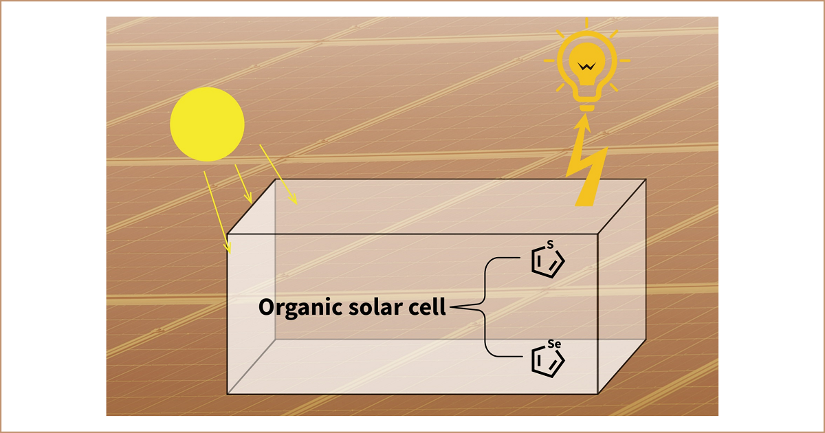
  • Solar cells;
  • Field-effect transistors;
  • Light-emitting diodes;
  • Photodetectors;
  • Fluorescent sensors;
  • Up-conversion luminescence;
  • Flexible electronics.

Prof. Dr. Shiming Zhang
Prof. Dr. Feng Xu
Dr. Clement Cabanetos
Guest Editors

Manuscript Submission Information

Manuscripts should be submitted online at www.mdpi.com by registering and logging in to this website. Once you are registered, click here to go to the submission form. Manuscripts can be submitted until the deadline. All submissions that pass pre-check are peer-reviewed. Accepted papers will be published continuously in the journal (as soon as accepted) and will be listed together on the special issue website. Research articles, review articles as well as short communications are invited. For planned papers, a title and short abstract (about 100 words) can be sent to the Editorial Office for announcement on this website.

Submitted manuscripts should not have been published previously, nor be under consideration for publication elsewhere (except conference proceedings papers). All manuscripts are thoroughly refereed through a single-blind peer-review process. A guide for authors and other relevant information for submission of manuscripts is available on the Instructions for Authors page. Materials is an international peer-reviewed open access semimonthly journal published by MDPI.

Please visit the Instructions for Authors page before submitting a manuscript. The Article Processing Charge (APC) for publication in this open access journal is 2600 CHF (Swiss Francs). Submitted papers should be well formatted and use good English. Authors may use MDPI's English editing service prior to publication or during author revisions.

Keywords

  • solar cells
  • field-effect transistors
  • light-emitting diodes
  • photodetectors
  • fluorescent sensors
  • up-conversion luminescence
  • flexible electronics

Published Papers (7 papers)

Order results
Result details
Select all
Export citation of selected articles as:

Research

Jump to: Review

11 pages, 2234 KiB  
Communication
The Role of Carbon in Metal–Organic Chemical Vapor Deposition-Grown MoS2 Films
by Tianyu Hou, Di Li, Yan Qu, Yufeng Hao and Yun Lai
Materials 2023, 16(21), 7030; https://doi.org/10.3390/ma16217030 - 03 Nov 2023
Viewed by 867
Abstract
Acquiring homogeneous and reproducible wafer-scale transition metal dichalcogenide (TMDC) films is crucial for modern electronics. Metal–organic chemical vapor deposition (MOCVD) offers a promising approach for scalable production and large-area integration. However, during MOCVD synthesis, extraneous carbon incorporation due to organosulfur precursor pyrolysis is [...] Read more.
Acquiring homogeneous and reproducible wafer-scale transition metal dichalcogenide (TMDC) films is crucial for modern electronics. Metal–organic chemical vapor deposition (MOCVD) offers a promising approach for scalable production and large-area integration. However, during MOCVD synthesis, extraneous carbon incorporation due to organosulfur precursor pyrolysis is a persistent concern, and the role of unintentional carbon incorporation remains elusive. Here, we report the large-scale synthesis of molybdenum disulfide (MoS2) thin films, accompanied by the formation of amorphous carbon layers. Using Raman, photoluminescence (PL) spectroscopy, and transmission electron microscopy (TEM), we confirm how polycrystalline MoS2 combines with extraneous amorphous carbon layers. Furthermore, by fabricating field-effect transistors (FETs) using the carbon-incorporated MoS2 films, we find that traditional n-type MoS2 can transform into p-type semiconductors owing to the incorporation of carbon, a rare occurrence among TMDC materials. This unexpected behavior expands our understanding of TMDC properties and opens up new avenues for exploring novel device applications. Full article
(This article belongs to the Special Issue Advances of Photoelectric Functional Materials and Devices)
Show Figures

Figure 1

11 pages, 2923 KiB  
Article
Localized Surface Plasmon-Enhanced Infrared-to-Visible Upconversion Devices Induced by Ag Nanoparticles
by Yuyi Zhang, Chengjun Liu, Xingyu Liu, Ziyu Wei, Hui Tao, Feng Xu, Lixi Wang, Jiangyong Pan, Wei Lei and Jing Chen
Materials 2023, 16(5), 1973; https://doi.org/10.3390/ma16051973 - 28 Feb 2023
Cited by 2 | Viewed by 1465
Abstract
Upconversion devices (UCDs) have motivated tremendous research interest with their excellent potential and promising application in photovoltaic sensors, semiconductor wafer detection, biomedicine, and light conversion devices, especially near-infrared-(NIR)-to-visible upconversion devices. In this research, a UCD that directly turned NIR light located at 1050 [...] Read more.
Upconversion devices (UCDs) have motivated tremendous research interest with their excellent potential and promising application in photovoltaic sensors, semiconductor wafer detection, biomedicine, and light conversion devices, especially near-infrared-(NIR)-to-visible upconversion devices. In this research, a UCD that directly turned NIR light located at 1050 nm into visible light located at 530 nm was fabricated to investigate the underlying working mechanism of UCDs. The simulation and experimental results of this research proved the existence of the quantum tunneling phenomenon in UCDs and found that the quantum tunneling effect can be enhanced by a localized surface plasmon. Full article
(This article belongs to the Special Issue Advances of Photoelectric Functional Materials and Devices)
Show Figures

Figure 1

10 pages, 1590 KiB  
Article
S⋯N Conformational Lock Acceptor Based on Indacenodithiophene (IDT) Structure and High Electronegative Terminal End Group
by Jiejun Zhu, Zhangxu Wang, Yuanhao Li, Xuan Liu, Chunyang Miao, Bo Wu and Shiming Zhang
Materials 2022, 15(12), 4238; https://doi.org/10.3390/ma15124238 - 15 Jun 2022
Cited by 1 | Viewed by 1178
Abstract
High-performance organic semiconductors should have good spectral absorption, a narrow energy gap, excellent thermal stability and good blend film morphology to obtain high-performance organic photovoltaics (OPVs). Therefore, we synthesized two IDTz-based electron acceptors in this research. When they were blended with donor PTB7-Th [...] Read more.
High-performance organic semiconductors should have good spectral absorption, a narrow energy gap, excellent thermal stability and good blend film morphology to obtain high-performance organic photovoltaics (OPVs). Therefore, we synthesized two IDTz-based electron acceptors in this research. When they were blended with donor PTB7-Th to prepare OPV devices, the PTB7-Th:IDTz-BARO-based binary OPVs exhibited a power conversion efficiency (PCE) of 0.37%, with a short-circuit current density (Jsc) of 1.24 mA cm−2, a fill factor (FF) of 33.99% and an open-circuit voltage (Voc) of 0.87 V. The PTB7-Th:IDTz-BARS-based binary OPVs exhibited PCE of 4.39%, with Jsc of 8.09 mA cm−2, FF of 54.13% and Voc of 1.00 V. The results show the strong electronegativity terminal group to be beneficial to the construction of high-performance OPV devices. Highlights: (1) Two new acceptors based on 5,5′-(4,4,9,9-tetrakis (4-hexylphenyl)-4,9-dihydro-s-indaceno [1,2-b:5,6-b′] dithiophene-2,7-diyl) dithiazole (IDTz) and different end groups (BARS, BARO) were synthesized; (2) BARS and BARO are electron-rich end groups, and the electron acceptors involved in the construction show excellent photoelectric properties. They can properly match the donor PTB7-Th, and show the appropriate surface morphology of the active layer in this work; (3) Compared with IDTz-BARO, IDTz-BARS has deeper LUMO and HOMO energy levels. In combination with PTB7-Th, it shows 4.39% device efficiency, 8.09 mA cm−2 short-circuit current density and 1.00 V open circuit voltage. Full article
(This article belongs to the Special Issue Advances of Photoelectric Functional Materials and Devices)
Show Figures

Figure 1

6 pages, 1793 KiB  
Article
Dual-Facets Emissive Quantum-Dot Light-Emitting Diode Based on AZO Electrode
by Jing Chen, Qianqian Huang and Wei Lei
Materials 2022, 15(3), 740; https://doi.org/10.3390/ma15030740 - 19 Jan 2022
Cited by 4 | Viewed by 1427
Abstract
We report on a green, dual emissive quantum-dot light-emitting diode (QLED) using alumina (Al)-doped ZnO (AZO) to adjust the band offset between the cathode and QD-emitting layers. The dual emissive QLED structure was designed by enhancing the efficient hole injection/transfer and slowing down [...] Read more.
We report on a green, dual emissive quantum-dot light-emitting diode (QLED) using alumina (Al)-doped ZnO (AZO) to adjust the band offset between the cathode and QD-emitting layers. The dual emissive QLED structure was designed by enhancing the efficient hole injection/transfer and slowing down the electron injection/transfer from AZO to the QD. The QLEDs presented a maximum luminance of 9450 cd/m2, corresponding to a power efficiency of 15.7 lm/W, a current efficiency of 25.5 cd/A, as well as a turn-on voltage of 2.3 V. It is worth noting that the performance of the dual emissive QLED is comparable to that of a single emissive QLED. Therefore, there is a 1.3-fold enhancement in the performance of the QLED based on the AZO cathode due to the balanced charge injection/transfer. Full article
(This article belongs to the Special Issue Advances of Photoelectric Functional Materials and Devices)
Show Figures

Figure 1

Review

Jump to: Research

24 pages, 4600 KiB  
Review
Emerging Nonlinear Photocurrents in Lead Halide Perovskites for Spintronics
by Jianbin Chen, Hacer Koc, Shengkai Zhao, Kaiyu Wang, Lingfeng Chao and Mustafa Eginligil
Materials 2024, 17(8), 1820; https://doi.org/10.3390/ma17081820 - 16 Apr 2024
Viewed by 483
Abstract
Lead halide perovskites (LHPs) containing organic parts are emerging optoelectronic materials with a wide range of applications thanks to their high optical absorption, carrier mobility, and easy preparation methods. They possess spin-dependent properties, such as strong spin–orbit coupling (SOC), and are promising for [...] Read more.
Lead halide perovskites (LHPs) containing organic parts are emerging optoelectronic materials with a wide range of applications thanks to their high optical absorption, carrier mobility, and easy preparation methods. They possess spin-dependent properties, such as strong spin–orbit coupling (SOC), and are promising for spintronics. The Rashba effect in LHPs can be manipulated by a magnetic field and a polarized light field. Considering the surfaces and interfaces of LHPs, light polarization-dependent optoelectronics of LHPs has attracted attention, especially in terms of spin-dependent photocurrents (SDPs). Currently, there are intense efforts being made in the identification and separation of SDPs and spin-to-charge interconversion in LHP. Here, we provide a comprehensive review of second-order nonlinear photocurrents in LHP in regard to spintronics. First, a detailed background on Rashba SOC and its related effects (including the inverse Rashba–Edelstein effect) is given. Subsequently, nonlinear photo-induced effects leading to SDPs are presented. Then, SDPs due to the photo-induced inverse spin Hall effect and the circular photogalvanic effect, together with photocurrent due to the photon drag effect, are compared. This is followed by the main focus of nonlinear photocurrents in LHPs containing organic parts, starting from fundamentals related to spin-dependent optoelectronics. Finally, we conclude with a brief summary and future prospects. Full article
(This article belongs to the Special Issue Advances of Photoelectric Functional Materials and Devices)
Show Figures

Figure 1

26 pages, 4639 KiB  
Review
A Review on Multiple I-III-VI Quantum Dots: Preparation and Enhanced Luminescence Properties
by Ting Chen, Yuanhong Chen, Youpeng Li, Mengbiao Liang, Wenkui Wu and Yude Wang
Materials 2023, 16(14), 5039; https://doi.org/10.3390/ma16145039 - 17 Jul 2023
Cited by 3 | Viewed by 1885
Abstract
I-III-VI type QDs have unique optoelectronic properties such as low toxicity, tunable bandgaps, large Stokes shifts and a long photoluminescence lifetime, and their emission range can be continuously tuned in the visible to near-infrared light region by changing their chemical composition. Moreover, they [...] Read more.
I-III-VI type QDs have unique optoelectronic properties such as low toxicity, tunable bandgaps, large Stokes shifts and a long photoluminescence lifetime, and their emission range can be continuously tuned in the visible to near-infrared light region by changing their chemical composition. Moreover, they can avoid the use of heavy metal elements such as Cd, Hg and Pb and highly toxic anions, i.e., Se, Te, P and As. These advantages make them promising candidates to replace traditional binary QDs in applications such as light-emitting diodes, solar cells, photodetectors, bioimaging fields, etc. Compared with binary QDs, multiple QDs contain many different types of metal ions. Therefore, the problem of different reaction rates between the metal ions arises, causing more defects inside the crystal and poor fluorescence properties of QDs, which can be effectively improved by doping metal ions (Zn2+, Mn2+ and Cu+) or surface coating. In this review, the luminous mechanism of I-III-VI type QDs based on their structure and composition is introduced. Meanwhile, we focus on the various synthesis methods and improvement strategies like metal ion doping and surface coating from recent years. The primary applications in the field of optoelectronics are also summarized. Finally, a perspective on the challenges and future perspectives of I-III-VI type QDs is proposed as well. Full article
(This article belongs to the Special Issue Advances of Photoelectric Functional Materials and Devices)
Show Figures

Figure 1

23 pages, 3683 KiB  
Review
Recent Advances in Selenophene-Based Materials for Organic Solar Cells
by Xuan Liu, Xin Jiang, Kaifeng Wang, Chunyang Miao and Shiming Zhang
Materials 2022, 15(22), 7883; https://doi.org/10.3390/ma15227883 - 08 Nov 2022
Cited by 4 | Viewed by 2020
Abstract
Due to the low cost, light weight, semitransparency, good flexibility, and large manufacturing area of organic solar cells (OSCs), OSCs have the opportunity to become the next generation of solar cells in some specific applications. So far, the efficiency of the OSC device [...] Read more.
Due to the low cost, light weight, semitransparency, good flexibility, and large manufacturing area of organic solar cells (OSCs), OSCs have the opportunity to become the next generation of solar cells in some specific applications. So far, the efficiency of the OSC device has been improved by more than 20%. The optical band gap between the lowest unoccupied molecular orbital (LUMO) level and the highest occupied molecular orbital (HOMO) level is an important factor affecting the performance of the device. Selenophene, a derivative of aromatic pentacyclic thiophene, is easy to polarize, its LUMO energy level is very low, and hence the optical band gap can be reduced. In addition, the selenium atoms in selenophene and other oxygen atoms or sulfur atoms can form an intermolecular interaction, so as to improve the stacking order of the active layer blend film and improve the carrier transport efficiency. This paper introduces the organic solar active layer materials containing selenium benzene in recent years, which can be simply divided into donor materials and acceptor materials. Replacing sulfur atoms with selenium atoms in these materials can effectively reduce the corresponding optical band gap of materials, improve the mutual solubility of donor recipient materials, and ultimately improve the device efficiency. Therefore, the sulfur in thiophene can be completely replaced by selenium or oxygen of the same family, which can be used in the active layer materials of organic solar cells. This article mainly describes the application of selenium instead of sulfur in OSCs. Full article
(This article belongs to the Special Issue Advances of Photoelectric Functional Materials and Devices)
Show Figures

Figure 1

Back to TopTop