
Integrated Sensor Electronic Front-Ends with Self-X Capabilities


Abstract
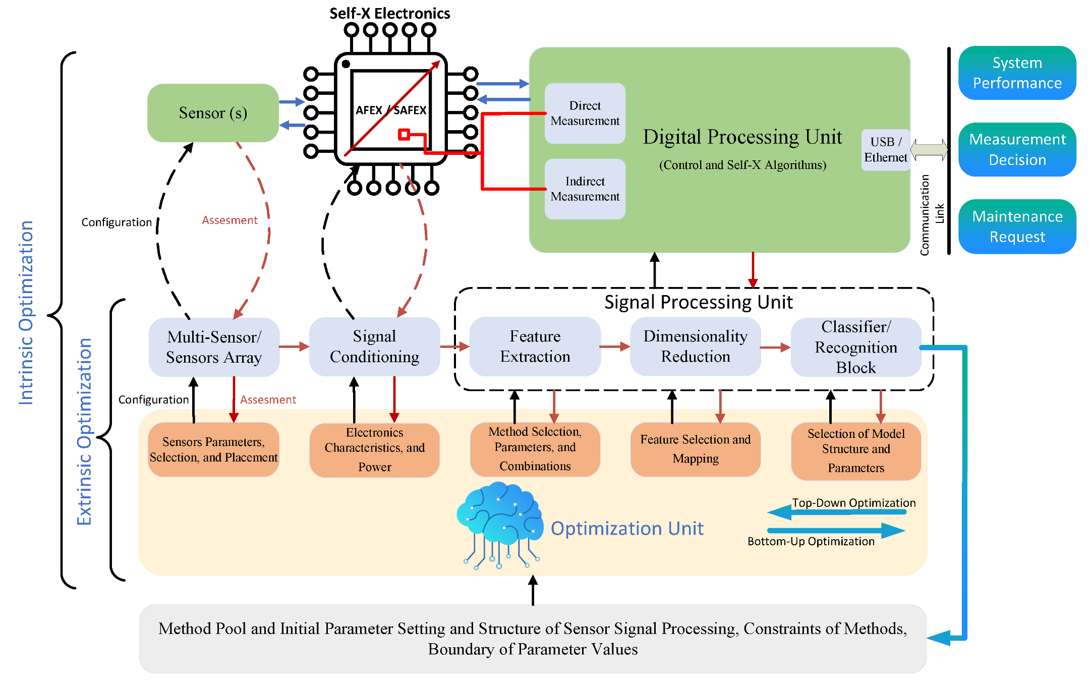
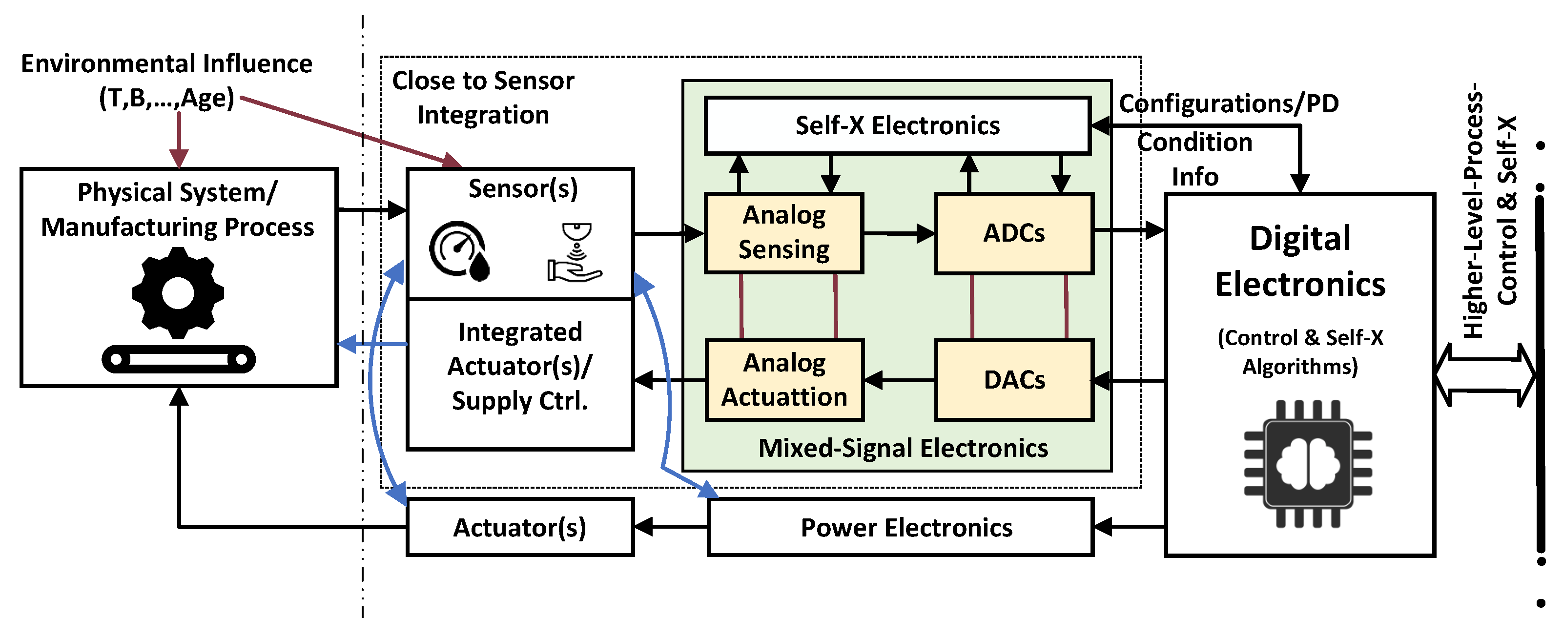
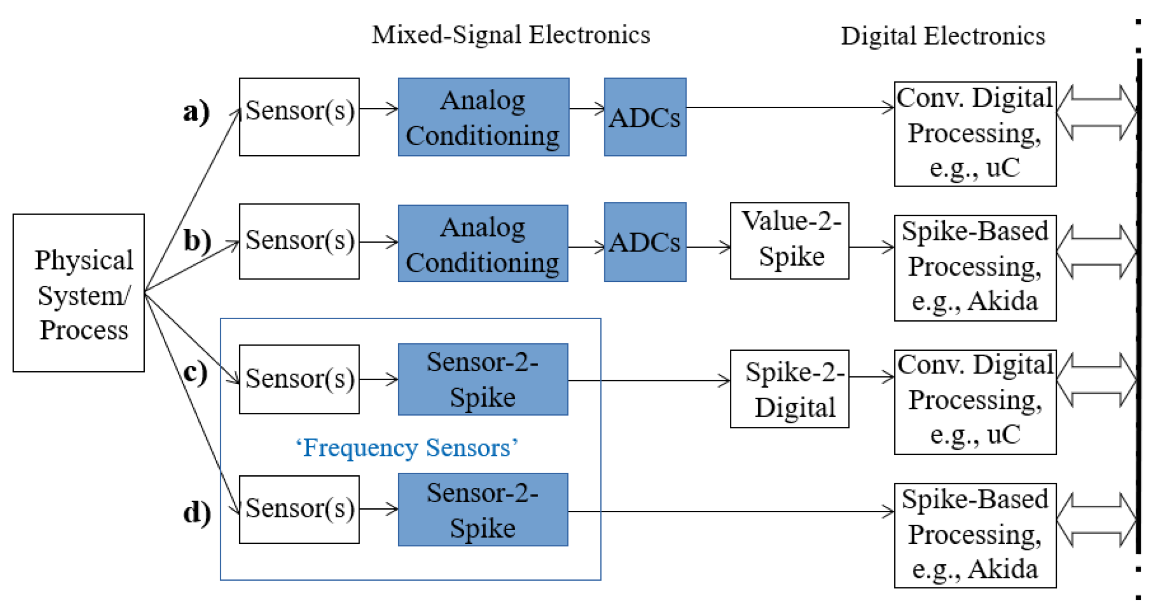
:1. Introduction
2. Survey of AFE in Industry and Research with Self-X Extension
3. Amplitude Domain AFEs with Self-X Extension
- The introduction of the fully differential analog circuits.
- The limitation of the reconfigurable circuit elements to the sensitive components only.
- The incorporation of cost-effective system performance evaluation setup based on indirect measurement methods to support the automatic test equipment (ATE).
- Alleviation of the observer uncertainty, mainly due to imperfections of the sensor and/or ADCs.
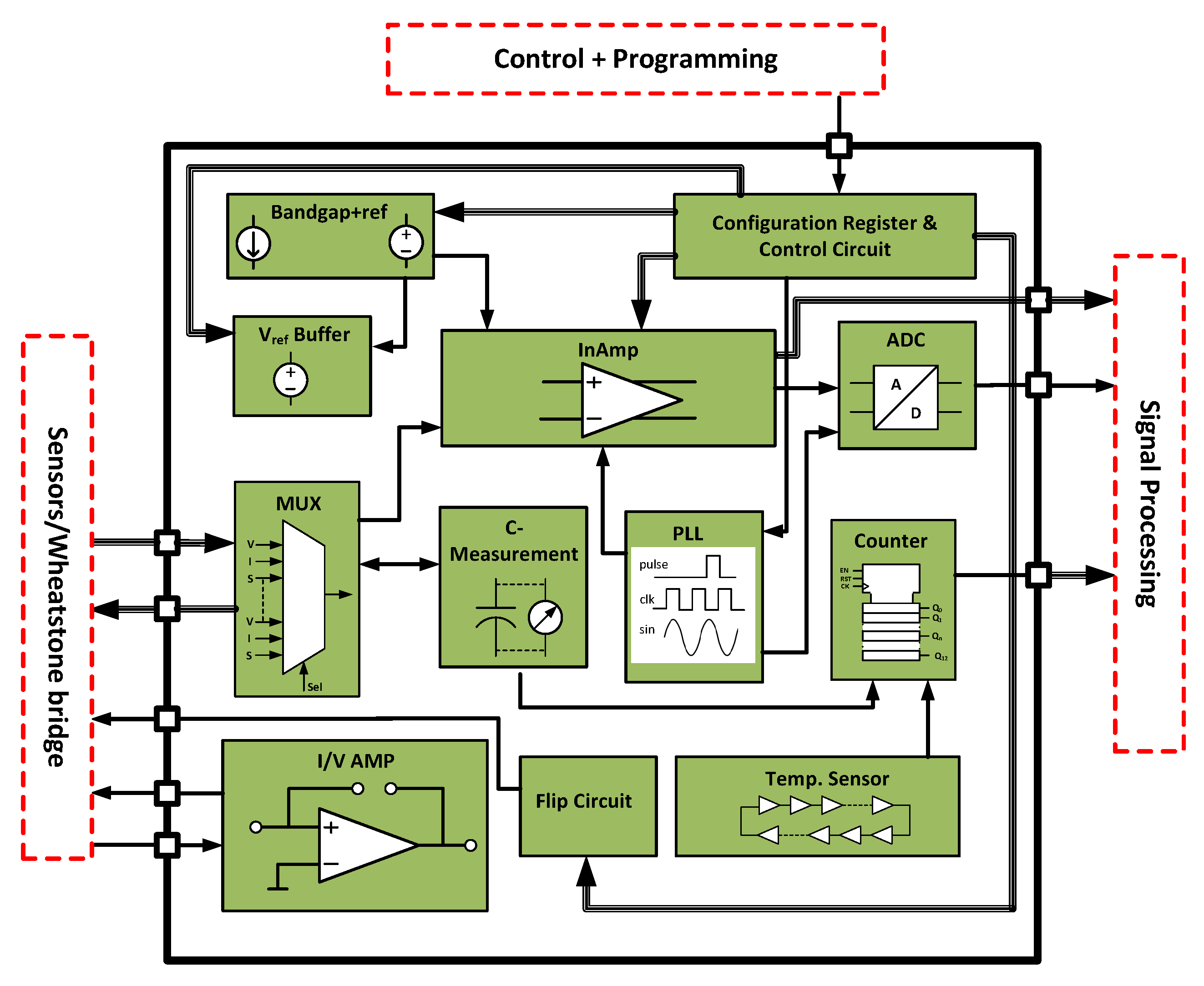
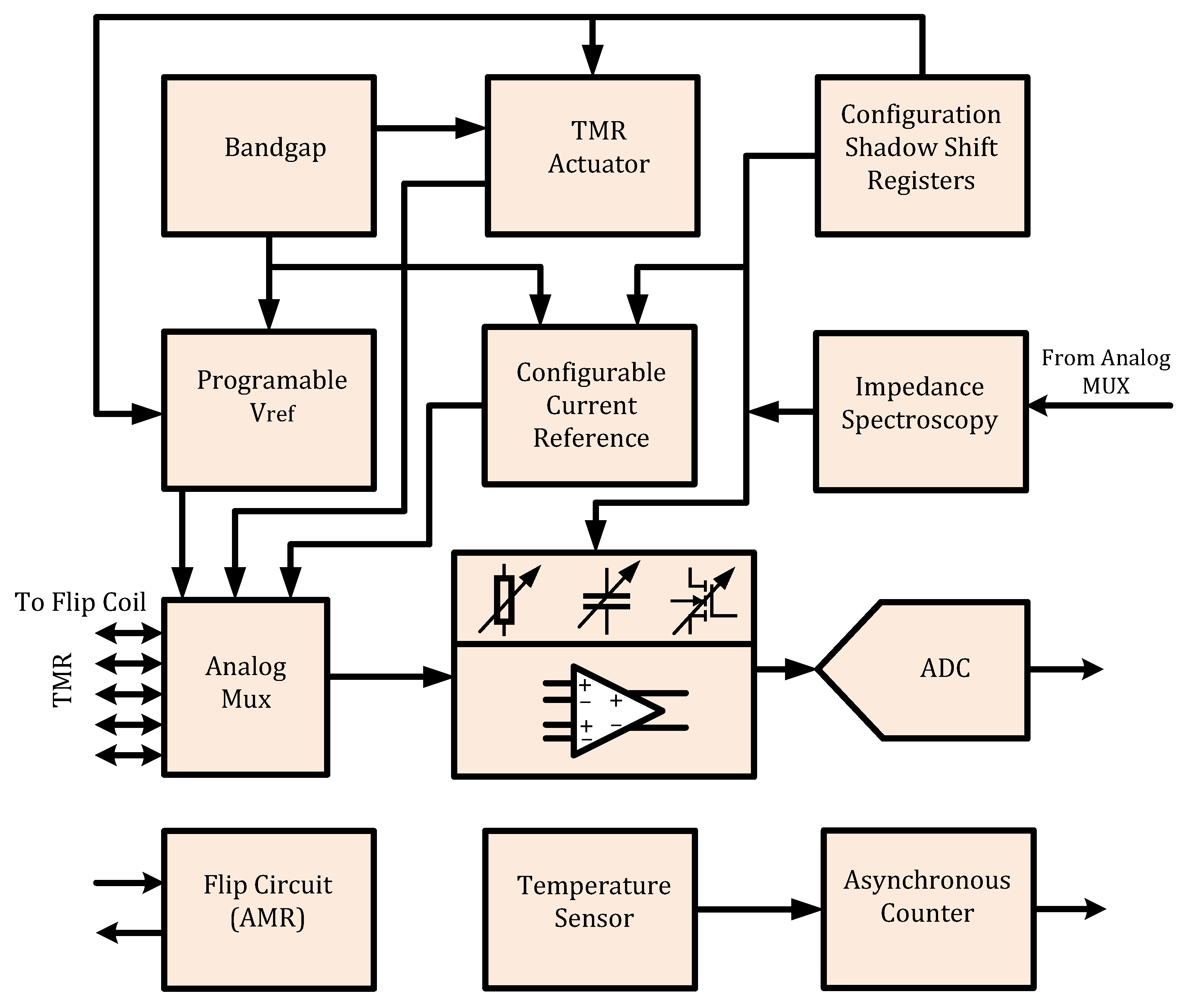
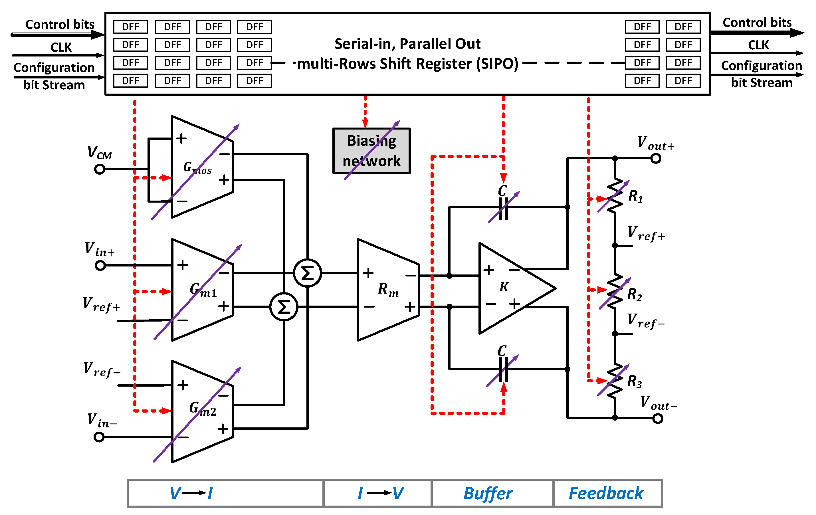
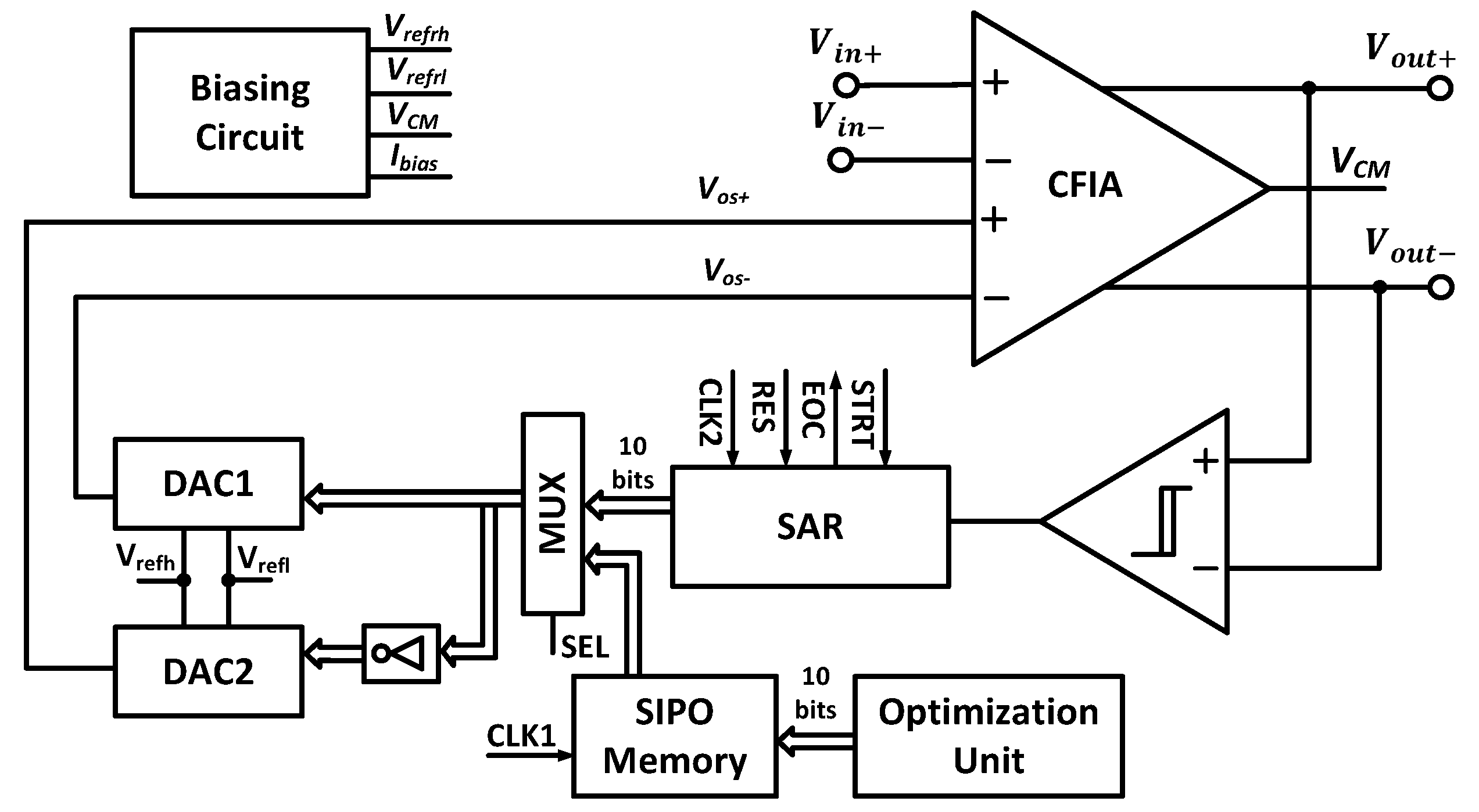
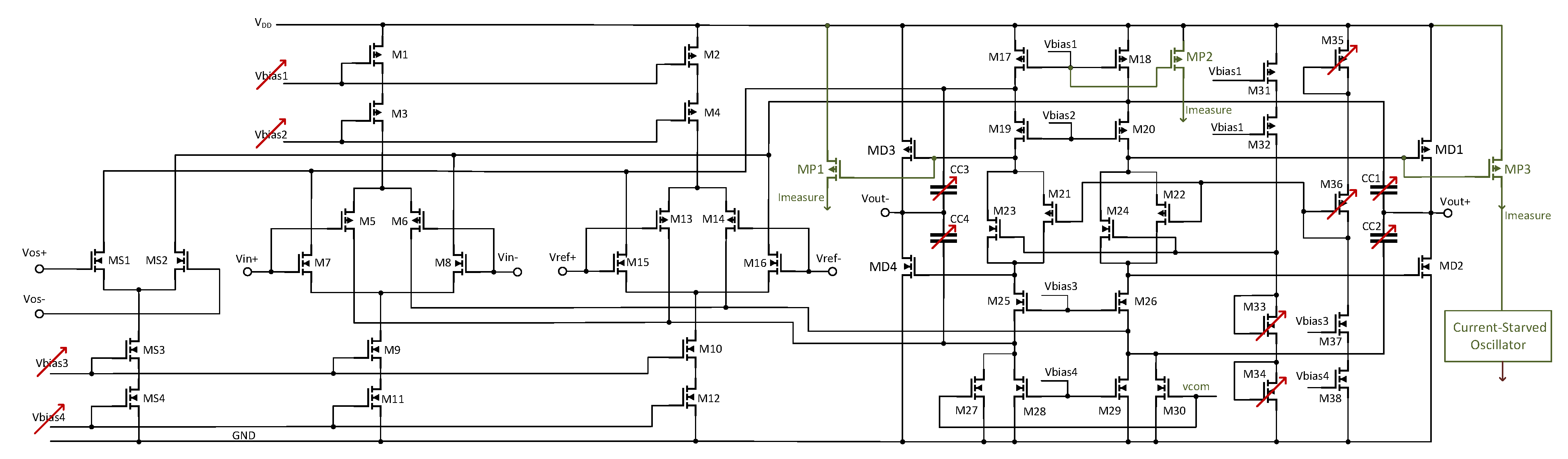
3.1. Instrumentation Amplifier
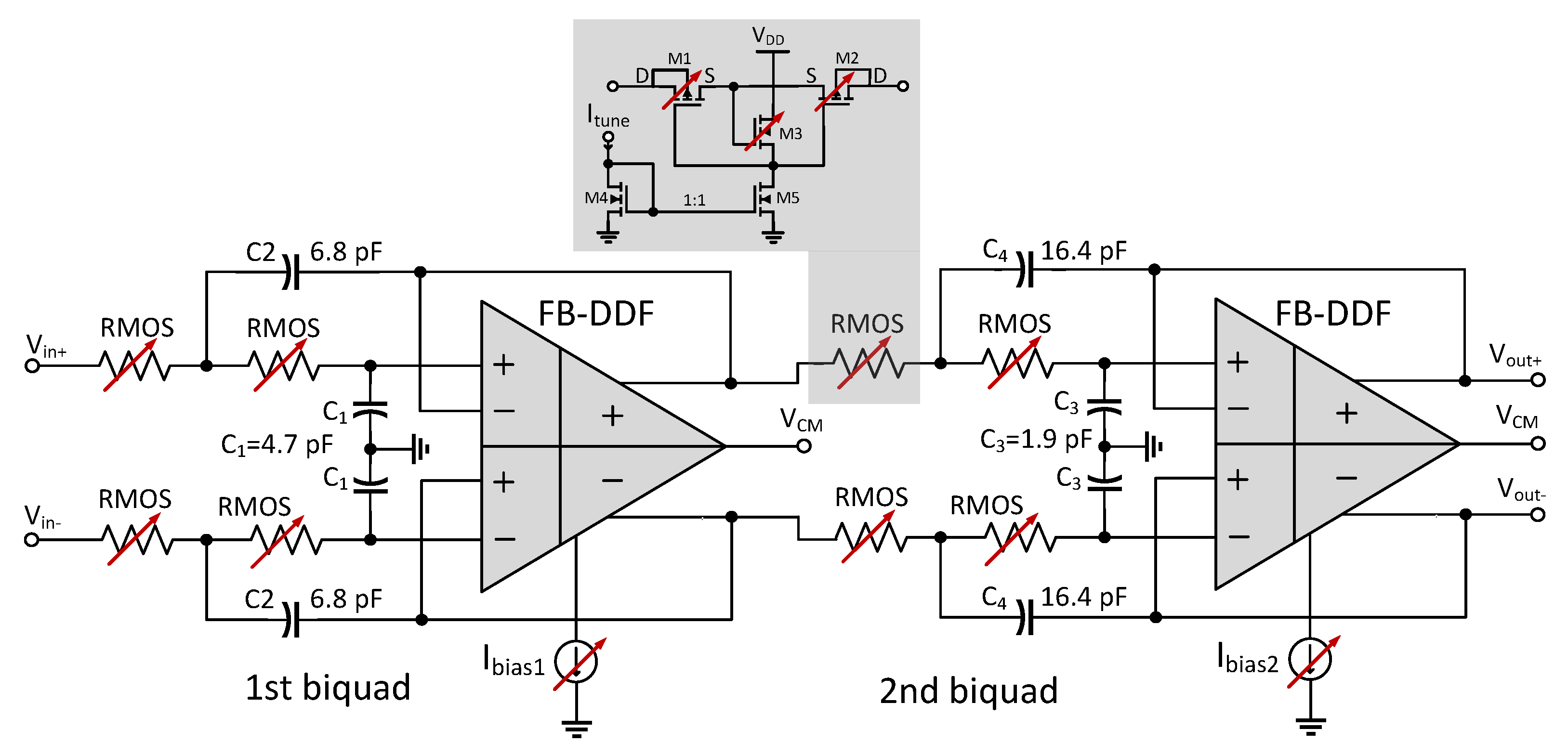
3.2. Anti-Aliasing Filter
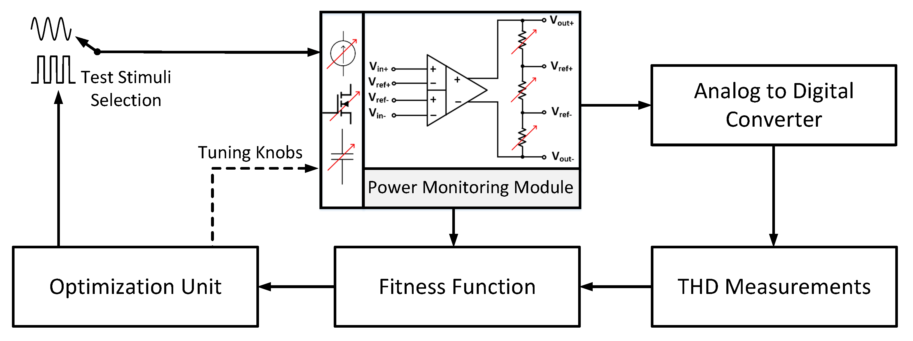
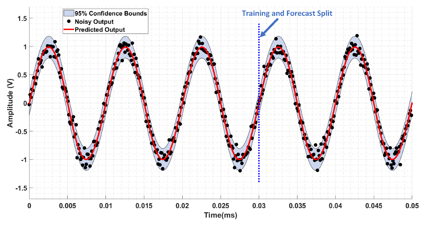
3.3. Assessment Unit
3.4. Optimization Unit
3.5. Observer Imperfections
4. Spiking AFEs with Self-X Extension
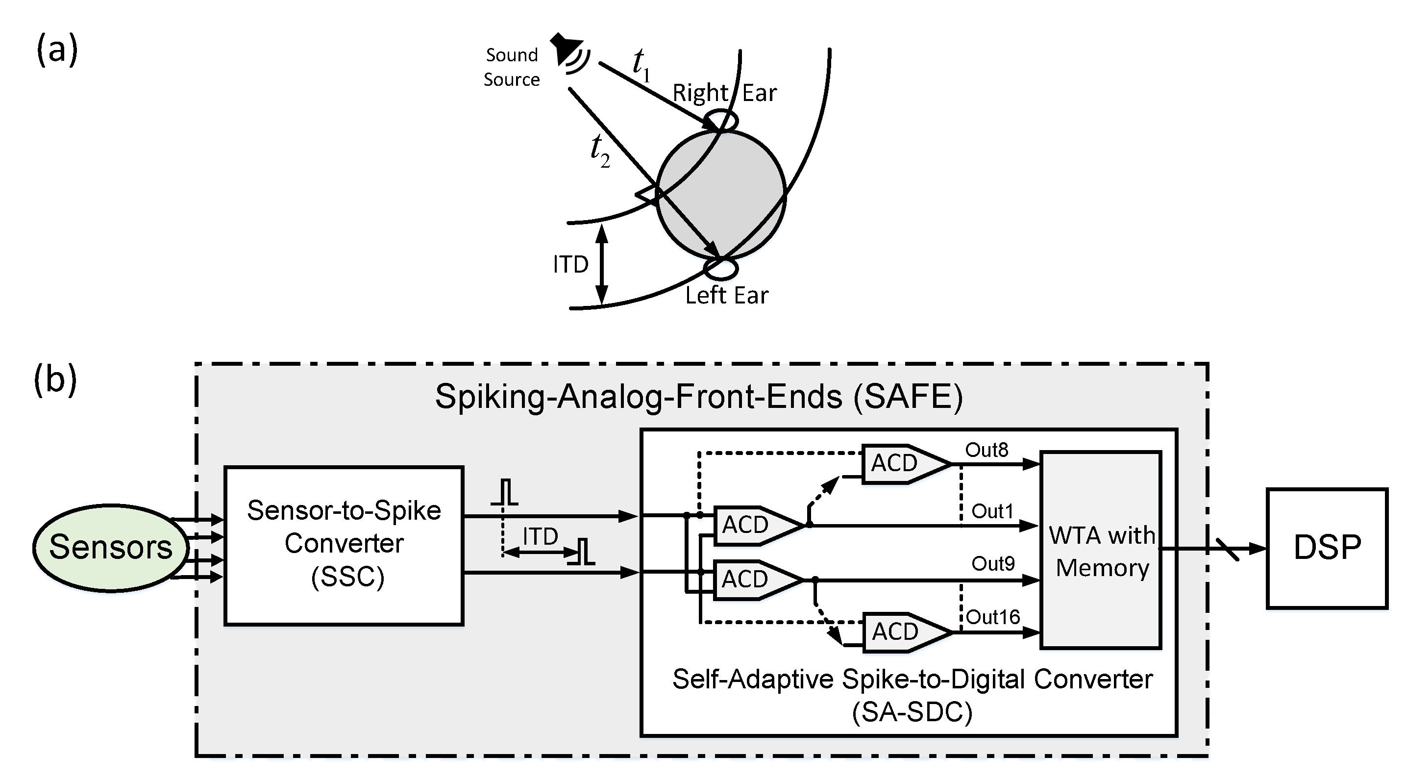
4.1. Natural Sensory Systems Evidence
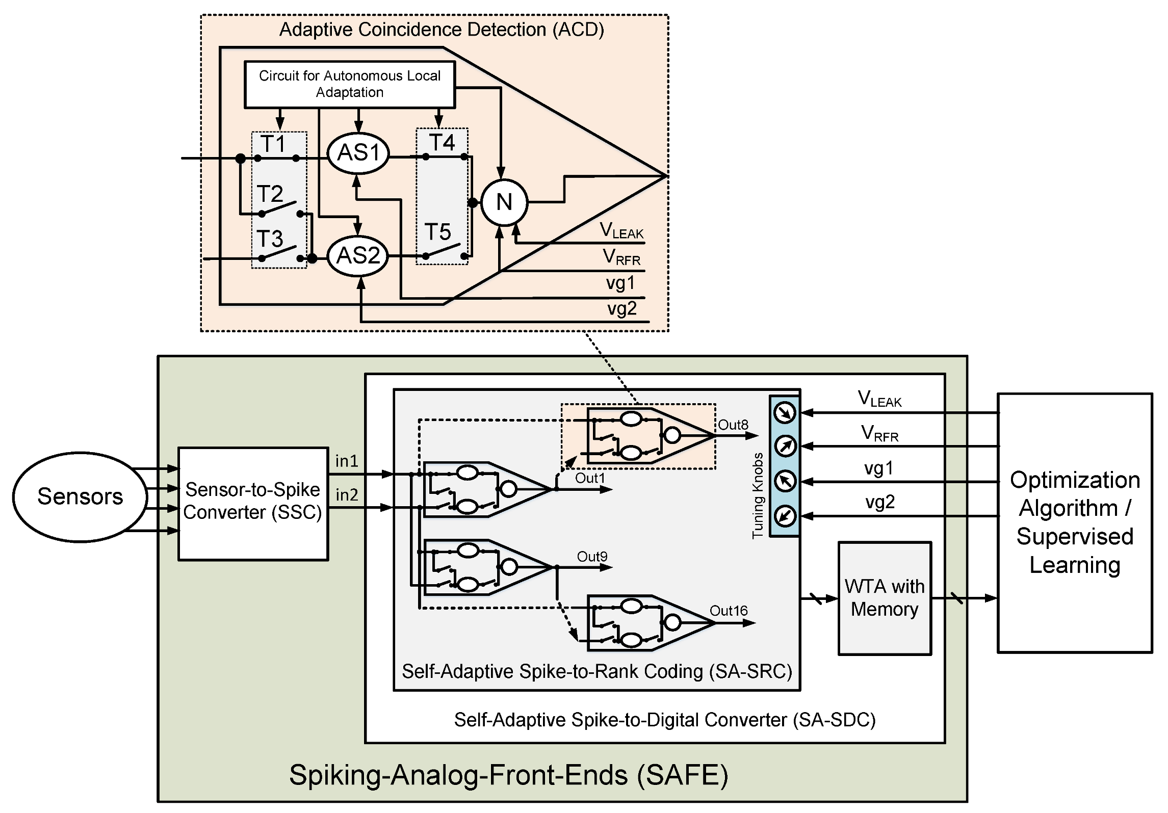
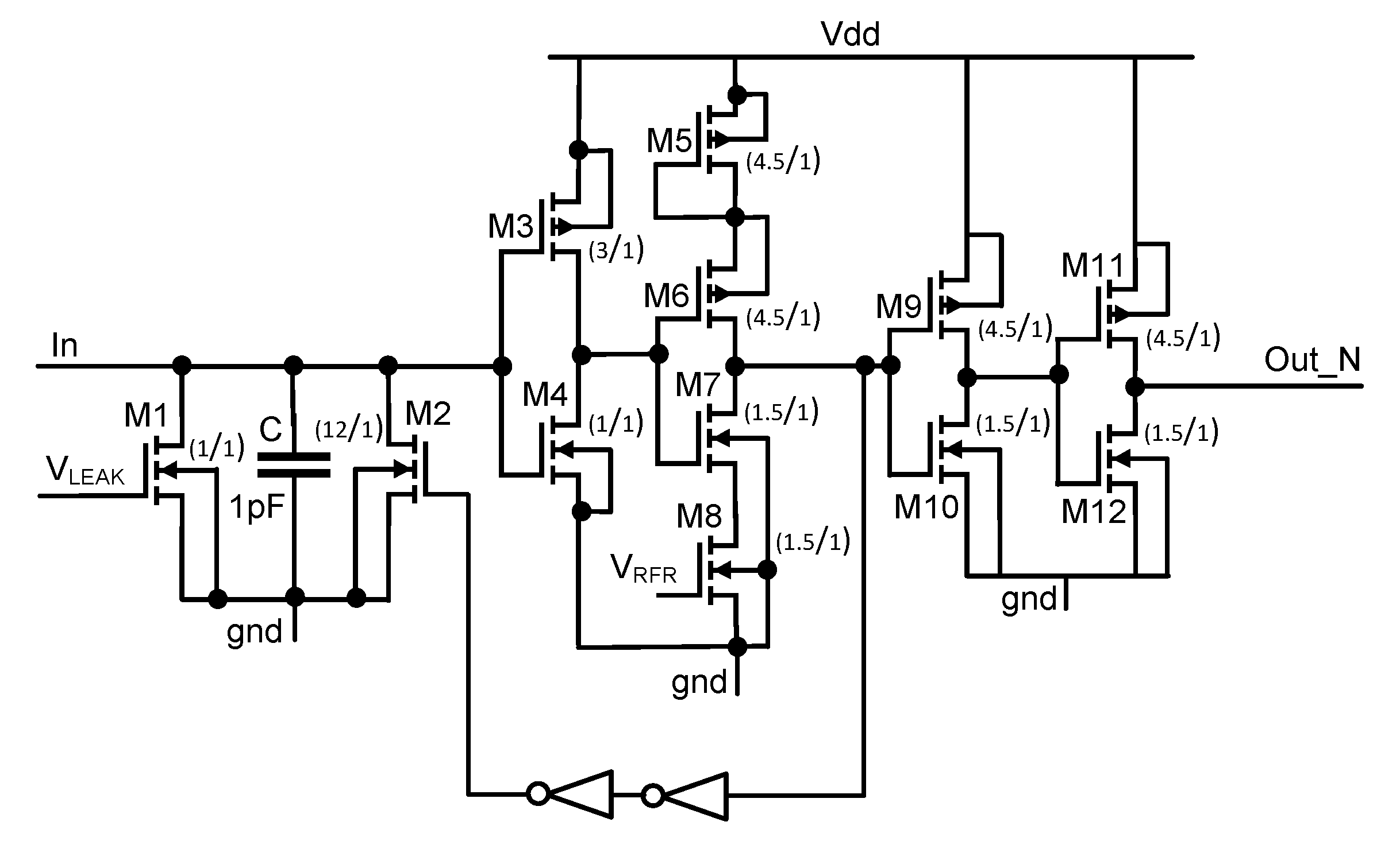
4.2. Proposed Self-Adaptive Spike-to-Digital Converter (SA-SDC)
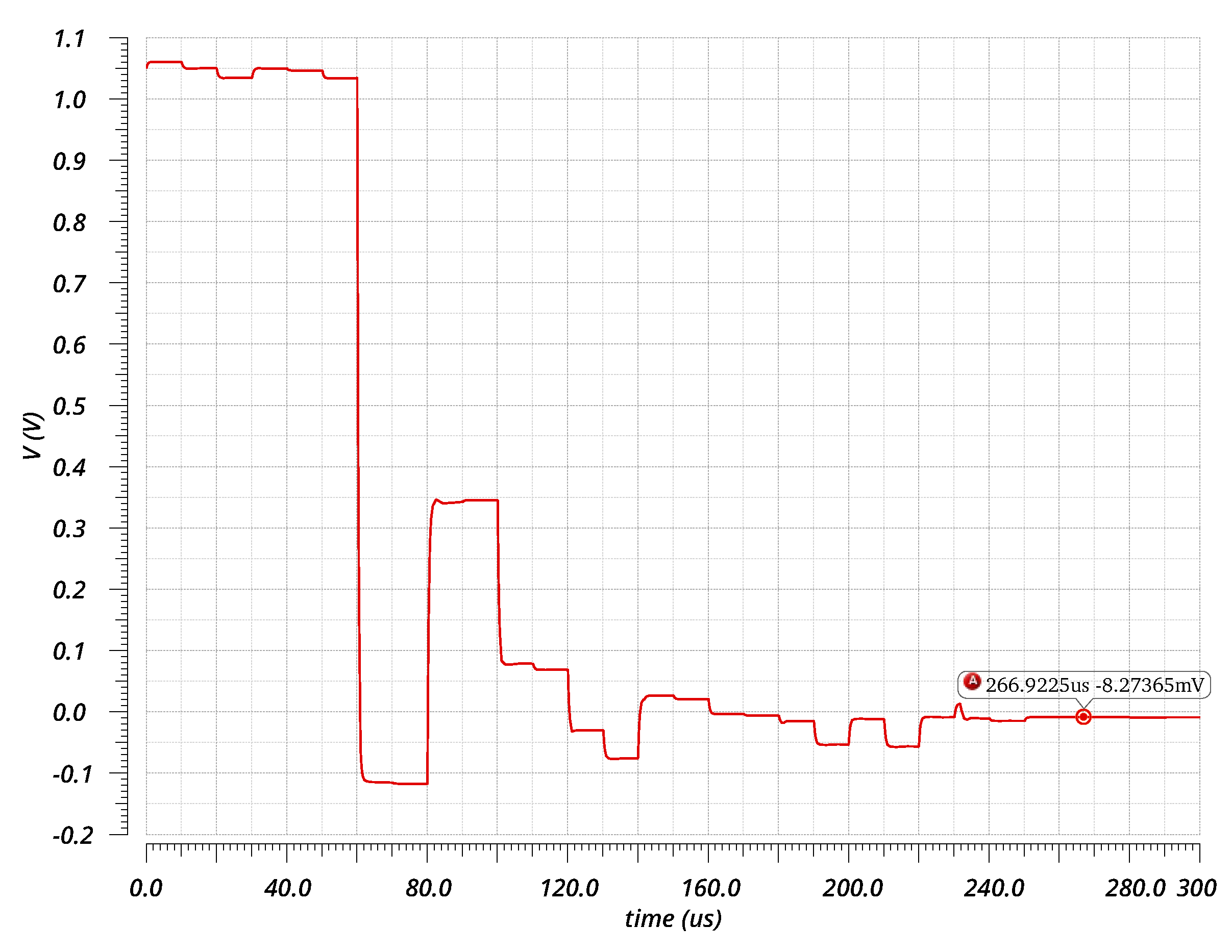
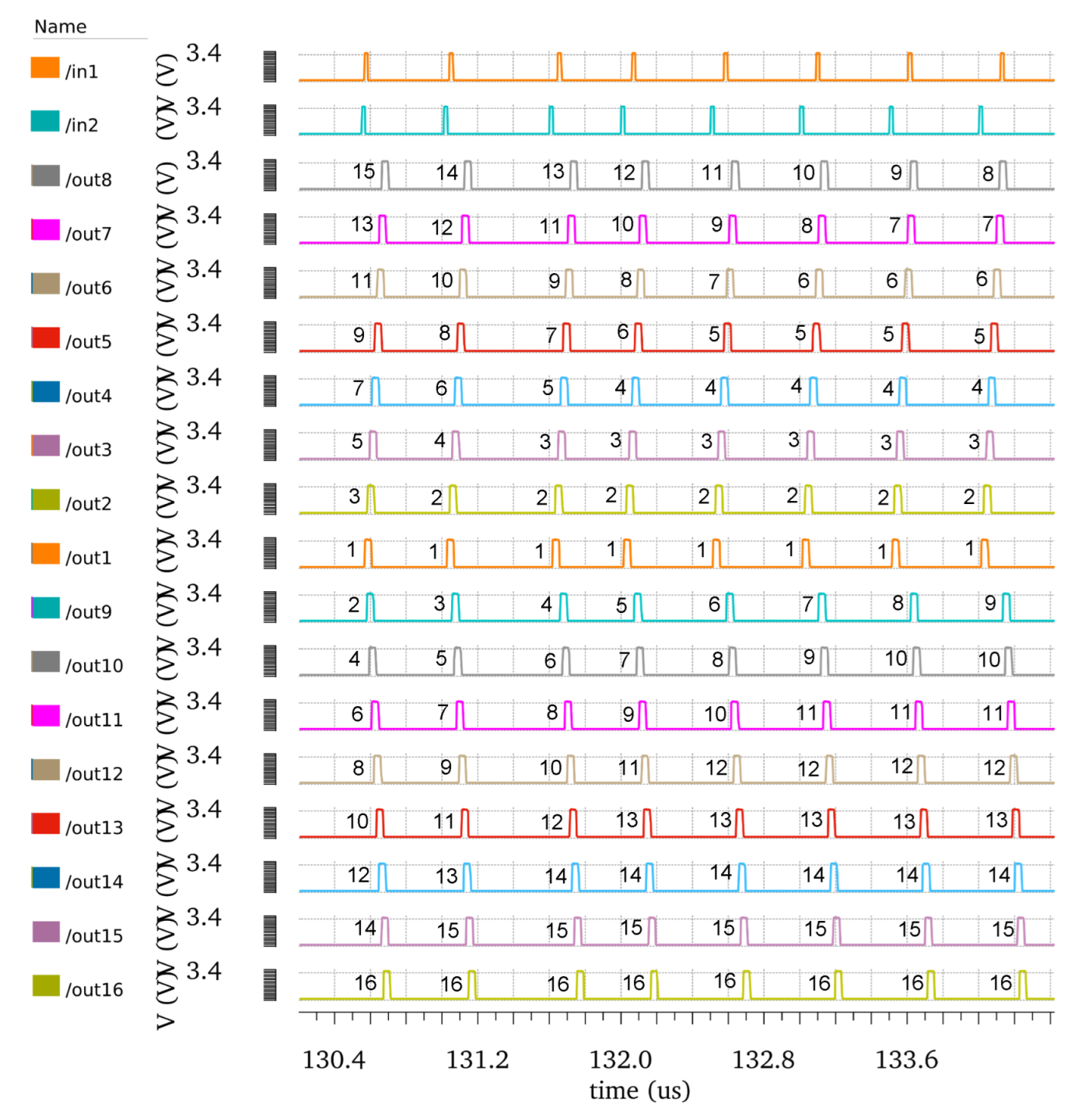
4.3. The Experimental Results
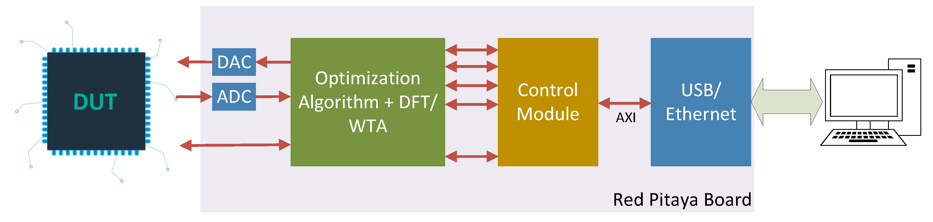
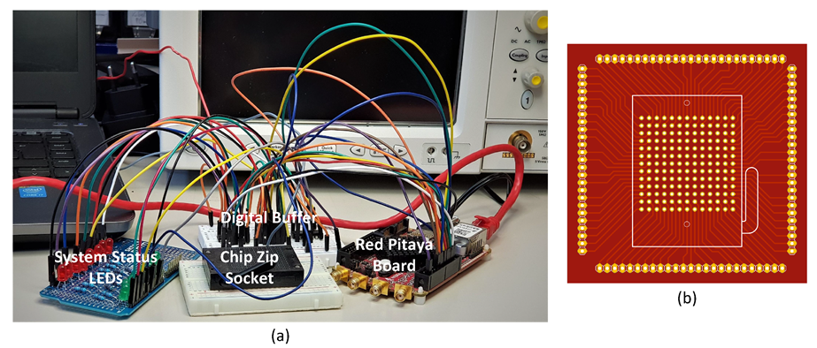
5. Chip and Demonstration Prototyping Board Design
- Investigation of the intrinsic optimization of our InAmp to retrieve extrinsic results for the manufactured instance.
- Applying the concept of robust optimization (archive-based and surrogate-based) for addressing the observer imperfections issues.
- Exploration of the LPF indirect performance optimization by using non-intrusive PVT sensors.
- Characterizing the basic operation of the neuron and synapse on the physical hardware level.
- Exploring the supervised and unsupervised optimization possibilities for the ACD and the SA-SRC.
6. Conclusions
Author Contributions
Funding
Institutional Review Board Statement
Informed Consent Statement
Data Availability Statement
Acknowledgments
Conflicts of Interest
Abbreviations
| AFE | Analog-front-ends |
| USIX | Universal-Sensor-Interface-with-self-X-properties |
| AFEX | Analog-front-ends with self-X properties |
| SAFEX | Spiking-analog-front-ends with self-X properties |
| CISS | Cognitive integrated sensory systems |
| SLM | Silicon Lifecycle Management |
| EHW | Evolvable hardware |
| PSO | Particle swarm optimization |
| ATE | Automatic test equipment |
| CFIA | Current-feedback in-amp |
| SIPO | Serial-in, parallel-out register |
| PPM | Power monitoring module |
| MHOAs | Meta-heuristic optimization algorithms |
| ERPSO | Experience replay particle swarm optimization |
| GPR | Gaussian process regression |
| OIs | Observer Imperfections |
| SSDC | Sensor to spike to digital converter |
| SSC | Sensor-to-spike converter |
| SDC | Spike-to-digital converter |
| ITDs | Interaural time differences |
| SA-SDC | Adaptive spike-to-digital converter |
| SA-SRC | Self-adaptive spike-to-rank coding |
| ACD | Adaptive coincidence detection |
| LIF | Leaky integrate and fire |
References
- IEEE. International Roadmap for Devices and Systems—More Moore. Available online: https://irds.ieee.org/images/files/pdf/2020/2020IRDS_MM.pdf (accessed on 11 March 2011).
- IEEE. International Roadmap for Devices and Systems—More than Moore. Available online: https://irds.ieee.org/images/files/pdf/2020/2020IRDS_MtM.pdf (accessed on 11 March 2011).
- Werthschützky, R. Sensor Technologien 2022; Technical Report; AMA Verband für Sensorik und Messtechnik e.V.: Göttingen, Germany, 2018. [Google Scholar]
- Goldstein, B.; Hendricks, J. NIST on a Chip. Available online: https://www.nist.gov/noac (accessed on 27 May 2022).
- Kagermann, H.; Lukas, W.; Wahlster, W. Industrie 4.0: Mit dem Internet der Dinge auf dem Weg zur 4. Industriellen Revolution; Technical Report 13; VDI Nachrichten: Heidelberg, Germany, 2011. [Google Scholar]
- Zhang, W.; Peng, G.; Li, C.; Chen, Y.; Zhang, Z. A New Deep Learning Model for Fault Diagnosis with Good Anti-Noise and Domain Adaptation Ability on Raw Vibration Signals. Sensors 2017, 17, 425. [Google Scholar] [CrossRef] [PubMed]
- Davies, M.; Srinivasa, N.; Lin, T.; Chinya, G.; Cao, Y.; Choday, S.H.; Dimou, G.; Joshi, P.; Imam, N.; Jain, S.; et al. Loihi: A Neuromorphic Manycore Processor with On-Chip Learning. IEEE Micro 2018, 38, 82–99. [Google Scholar] [CrossRef]
- DeBole, M.V.; Taba, B.; Amir, A.; Akopyan, F.; Andreopoulos, A.; Risk, W.P.; Kusnitz, J.; Otero, C.O.; Nayak, T.K.; Appuswamy, R.; et al. TrueNorth: Accelerating From Zero to 64 Million Neurons in 10 Years. Computer 2019, 52, 20–29. [Google Scholar] [CrossRef]
- BrainChip. Akida Neural Processor IP. Available online: https:brainchipinc.com/akida-neural-processor-ip/ (accessed on 28 September 2021).
- Moore, S.K. Supersize AI: Cerebra’s silicon-wafer-size chip boasts 2.6 trillion transistors. IEEE Spectr. 2021, 58, 12–13. [Google Scholar] [CrossRef]
- König, A.; Eberhardt, M.; Wenzel, R. QuickCog Self-Learning Recognition System—Exploiting machine learning techniques for transparent and fast industrial recognition system design. Image Process. Eur. 1999, 10–19. [Google Scholar]
- Thongpull, K.; König, A. Advance and case studies of the DAICOX framework for automated design of multi-sensor intelligent measurement systems. Tech. Mess. 2016, 83, 234–243. [Google Scholar] [CrossRef]
- Peters, S.; König, A. Optimized texture operators for the automated design of image analysis systems: Non-linear and oriented kernels vs. gray value co-occurrence matrices. Int. J. Hybrid Intell. Syst. 2007, 4, 185–202. [Google Scholar] [CrossRef]
- Eberhardt, M.; Roth, S.; König, A. Industrial Application of Machine-in-the-Loop-Learning for a Medical Robot Vision System—Concept and Comprehensive Field Study. Comput. Electr. Eng. (CEE) 2008, 34, 111–126. [Google Scholar] [CrossRef]
- Iswandy, K.; König, A. Methodology, Algorithms, and Emerging Tool for Automated Design of Intelligent Integrated Multi-Sensor Systems. J. Algorithms 2009, 8, 1368–1409. [Google Scholar] [CrossRef]
- MUNEDA. WiCkeD EDA Tools for Process Migration, Sizing, and Verification of Custom IC. Available online: https:www.muneda.com/ (accessed on 27 May 2022).
- Brooks, S.; Roy, R. An overview of self-engineering systems. J. Eng. Des. 2021, 32, 397–447. [Google Scholar] [CrossRef]
- Sapozhnikova, K.; Baksheeva, I.; Taymanov, R. Features and experience of metrological self-check organisation in multichannel measuring system. In Proceedings of the 2020 XXX International Scientific Symposium Metrology and Metrology Assurance (MMA), Sozopol, Bulgaria, 7–11 September 2020; pp. 1–5. [Google Scholar] [CrossRef]
- König, A. Integrated Sensor Electronics with Self-X Capabilities for Advanced Sensory Systems as a Baseline for Industry 4. In 0. In Proceedings of the Sensors and Measuring Systems, 19th ITG/GMA-Symposium, Nuremberg, Germany, 26–27 June 2018; pp. 1–4. [Google Scholar]
- König, A. Self-X Sensory Systems: Robust Information Representation and Processing in Adaptive Architecture. In Proceedings of the Invited Talk, 10. VDI-Fachtagung Messunsicherheit Praxisgerecht Bestimmen—Prüfprozesse in der Industriellen Praxis, Der Weg zum Sicheren Messen und Prüfen, Erfurt, Germany, 10–11 November 2021; VDI-Berichte: Dusseldorf, Germany, 2021; pp. 247–251. [Google Scholar]
- In-Chip Monitoring and Sensing. Available online: https://www.synopsys.com/solutions/silicon-lifecycle-management/in-chip-monitoring-and-sensing.html (accessed on 19 May 2022).
- Kashyap, R. Silicon lifecycle management (SLM) with in-chip monitoring. In Proceedings of the 2021 IEEE International Reliability Physics Symposium (IRPS), Monterey, CA, USA, 21–25 March 2021; pp. 1–4. [Google Scholar] [CrossRef]
- Silicon Lifecycle Management: Actionable Silicon Insights Through Intelligent Measurement and Analysis. Available online: https://www.synopsys.com/solutions/silicon-lifecycle-management.html (accessed on 19 May 2022).
- Synopsys Expansion of Silicon Lifecycle Management Platform. Available online: https://www.eetasia.com/synopsys-acquires-moortec-to-expand-silicon-lifecycle-management-platform/ (accessed on 19 May 2022).
- Stoica, A. Evolvable hardware: From on-chip circuit synthesis to evolvable space systems. In Proceedings of the 30th IEEE International Symposium on Multiple-Valued Logic (ISMVL 2000), Portland, OR, USA, 25 May 2000; pp. 161–169. [Google Scholar] [CrossRef]
- Johar, M.A.; Freier, R.; König, A. Adding self-x capabilities to AMR sensors as a first step towards dependable embedded systems. In Proceedings of the 2011 Ninth International Workshop on Intelligent Solutions in Embedded Systems, Regensburg, Germany, 7–8 July 2011; pp. 41–46. [Google Scholar]
- Kammara, A.C.; König, A.; Graef, T.; Chinazzo, A.; Dobariya, C.; Casper, F.; Paul, J.; Glenske, C.; Traute, J. Co-Design of MR Sensor and Sensor Electronics for Self-X Integrated Sensory Systems. In Proceedings of the Sensors and Measuring Systems, 19th ITG/GMA-Symposium, Nuremberg, Germany, 26–27 June 2018; pp. 1–4. [Google Scholar]
- Tawdross, P.; König, A. Mixtrinsic Multi-Objective Reconfiguration of Evolvable Sensor Electronics. In Proceedings of the Second NASA/ESA Conference on Adaptive Hardware and Systems (AHS 2007), Edinburgh, UK, 5–8 August 2007; pp. 51–57. [Google Scholar]
- Okamoto, T.; Ishida, Y. An Immunity-Based Anomaly Detection System with Sensor Agents. Sensors 2009, 9, 9175–9195. [Google Scholar] [CrossRef]
- Tokumitsu, M.; Hasegawa, K.; Ishida, Y. Resilient Sensor Networks with Spatiotemporal Interpolation of Missing Sensors: An Example of Space Weather Forecasting by Multiple Satellites. Sensors 2016, 16, 548. [Google Scholar] [CrossRef] [PubMed]
- Hong, L. Artificial Immune System for Anomaly Detection. In Proceedings of the 2008 IEEE International Symposium on Knowledge Acquisition and Modeling Workshop, Wuhan, China, 21–22 December 2008; pp. 340–343. [Google Scholar] [CrossRef]
- Zuccolotto, M. Artificial Immune Intelligent Maintenance System. In Proceedings of the 2014 12th IEEE International Conference on Industrial Informatics (INDIN), Porto Alegre, Brazil, 27–30 July 2014; pp. 795–798. [Google Scholar] [CrossRef]
- Alizadeh, E.; Meskin, N.; Khorasani, K. A sensor fault detection and isolation strategy by using a Dendritic Cell Algorithm. In Proceedings of the 2016 IEEE International Conference on Systems, Man and Cybernetics (SMC), Budapest, Hungary, 9–12 October 2016; pp. 001171–001177. [Google Scholar] [CrossRef]
- Döge, J.; Schonfelder, G.; Streil, G.T.; König, A. An HDR CMOS image sensor with spiking pixels, pixel-level ADC, and linear characteristics. IEEE Trans. Circuits Syst. II Analog. Digit. Signal Process. 2002, 49, 155–158. [Google Scholar] [CrossRef]
- Lichtsteiner, P.; Posch, C.; Delbruck, T. A 128 × 128 120 dB 15 μs Latency Asynchronous Temporal Contrast Vision Sensor. IEEE J. Solid-State Circuits 2008, 43, 566–576. [Google Scholar] [CrossRef]
- AMS. Compact AMS Time-to-Digital Converter Provides High Precision in Optical Ranging and 3D Scanning. Available online: https://ams-osram.com/news/press-releases/compact-ams-time-to-digital-converter-provides-high-precision-in-optical-ranging-and-3d-scanning (accessed on 27 May 2022).
- Mayr, C.; Partzsch, J.; Noack, M.; Schüffny, R. Configurable Analog-Digital Conversion Using the Neural Engineering Framework. Front. Neurosci. 2014, 8, 201. [Google Scholar] [CrossRef] [PubMed]
- Kammara, A.; König, A. SSDCα—Inherently robust integrated biomimetic sensor-to-spike-to-digital converter based on peripheral neural ensembles. Tech. Mess. 2016, 83, 531–542. [Google Scholar] [CrossRef]
- The 6X The New Radar Level Sensor. Available online: https://www.vega.com/en-de/radar (accessed on 19 May 2022).
- Lee, E.K.; Gulak, P.G. A CMOS field-programmable analog array. IEEE J. Solid-State Circuits 1991, 26, 1860–1867. [Google Scholar] [CrossRef]
- Lee, E.K.; Gulak, P.G. A transconductor-based field-programmable analog array. In Proceedings of the ISSCC’95-International Solid-State Circuits Conference, San Francisco, CA, USA, 15–17 February 1995; IEEE: Piscataway, NJ, USA, 1995; pp. 198–199. [Google Scholar]
- Stoica, A. Toward evolvable hardware chips: Experiments with a programmable transistor array. In Proceedings of the Seventh International Conference on Microelectronics for Neural, Fuzzy and Bio-Inspired Systems, Washington, DC, USA, 7–9 April 1999; IEEE: Piscataway, NJ, USA, 1999; pp. 156–162. [Google Scholar]
- Stoica, A.; Keymeulen, D.; Tawel, R.; Salazar-Lazaro, C.; Li, W.T. Evolutionary experiments with a fine-grained reconfigurable architecture for analog and digital CMOS circuits. In Proceedings of the First NASA/DoD Workshop on Evolvable Hardware, Pasadena, CA, USA, 19–21 July 1999; IEEE: Piscataway, NJ, USA, 1999; pp. 76–84. [Google Scholar]
- Stoica, A.; Zebulum, R.; Keymeulen, D. Progress and challenges in building evolvable devices. In Proceedings of the Third NASA/DoD Workshop on Evolvable Hardware—EH-2001, Long Beach, CA, USA, 12–14 July 2001; IEEE: Piscataway, NJ, USA, 2001; pp. 33–35. [Google Scholar]
- Langeheine, J.; Fölling, S.; Meier, K.; Schemmel, J. Towards a silicon primordial soup: A fast approach to hardware evolution with a VLSI transistor array. In Proceedings of the International Conference on Evolvable Systems, Edinburgh, UK, 17–19 April 2000; Springer: New York, NY, USA, 2000; pp. 123–132. [Google Scholar]
- Langeheine, J.; Becker, J.; Fölling, S.; Meier, K.; Schemmel, J. Initial studies of a new VLSI field programmable transistor array. In Proceedings of the International Conference on Evolvable Systems, Tokyo, Japan, 3–5 October 2001; Springer: New York, NY, USA, 2001; pp. 62–73. [Google Scholar]
- Higuchi, T.; Iwata, M.; Keymeulen, D.; Sakanashi, H.; Murakawa, M.; Kajitani, I.; Takahashi, E.; Toda, K.; Salami, N.; Kajihara, N.; et al. Real-world applications of analog and digital evolvable hardware. IEEE Trans. Evol. Comput. 1999, 3, 220–235. [Google Scholar] [CrossRef]
- Lakshmanan, S.; König, A. True Front-to-Back Analogue IC Designers’ Training. Int. J. Electr. Eng. Educ. 2010, 47, 277–292. [Google Scholar] [CrossRef]
- De Garis, H. ; Electrotechnical Lab Tsukuba. Genetic Programming-Evolutionary Approaches to Multistrategy Learning; Michalski, R.S., Tecuci, G., Eds.; Citeseer: Princeton, NJ, USA, 1994; Volume 4. [Google Scholar]
- Tanaka, H.; Niwa, T.; Tanaka, T.; Iba, H.; de Garis, H.; Furuya, T. Evolving hardware with genetic learning: A first step towards building a Darwin machine. In Proceedings of the 2nd International Conference on Simulated Adaptive Behaviour; MIT Press: Cambridge, MA, USA, 1993; Volume 2, p. 417. [Google Scholar]
- Thompson, A. Evolving electronic robot controllers that exploit hardware resources. In Proceedings of the European Conference on Artificial Life, Granada, Spain, 4–6 June 1995; Springer: New York, NY, USA; pp. 640–656. [Google Scholar]
- Sipper, M.; Sanchez, E.; Mange, D.; Tomassini, M.; Pérez-Uribe, A.; Stauffer, A. A phylogenetic, ontogenetic, and epigenetic view of bio-inspired hardware systems. IEEE Trans. Evol. Comput. 1997, 1, 83–97. [Google Scholar] [CrossRef]
- Thompson, A. Silicon evolution. In Proceedings of the 1st Annual Conference on Genetic Programming, Stanford, CA, USA, 28–31 July 1996; pp. 444–452. [Google Scholar]
- Yao, X.; Higuchi, T. Promises and challenges of evolvable hardware. IEEE Trans. Syst. Man Cybern. Part C 1999, 29, 87–97. [Google Scholar] [CrossRef]
- Kajitani, I.; Hoshino, T.; Nishikawa, D.; Yokoi, H.; Nakaya, S.; Yamauchi, T.; Inuo, T.; Kajihara, N.; Iwata, M.; Keymeulen, D.; et al. A gate-level EHW chip: Implementing GA operations and reconfigurable hardware on a single LSI. In Proceedings of the International Conference on Evolvable Systems, Lausanne, Switzerland, 23–25 September 1998; Springer: New York, NY, USA, 1998; pp. 1–12. [Google Scholar]
- Kajitani, I.; Hoshino, T.; Iwata, M.; Higuchi, T. Variable length chromosome GA for evolvable hardware. In Proceedings of the IEEE International Conference on Evolutionary Computation, Nagoya, Japan, 20–22 May 1996; IEEE: Piscataway, NJ, USA, 1996; pp. 443–447. [Google Scholar]
- De Garis, H. Genetic programming artificial nervous systems artificial embryos and embryological electronics. In Proceedings of the International Conference on Parallel Problem Solving from Nature, Dortmund, Germany, 1–3 October 1990; Springer: New York, NY, USA, 1990; pp. 117–123. [Google Scholar]
- de Garis, H. Evolvable hardware genetic programming of a Darwin machine. In Artificial Neural Nets and Genetic Algorithms; Springer: New York, NY, USA, 1993; pp. 441–449. [Google Scholar]
- Henson, B.; Walker, J.A.; Trefzer, M.A.; Tyrrell, A.M. Designing digital systems using Cartesian Genetic Programming and VHDL. In Inspired by Nature; Springer: New York, NY, USA, 2018; pp. 57–86. [Google Scholar]
- Hereford, J.; Pruitt, C. Robust sensor systems using evolvable hardware. In Proceedings of the 2004 NASA/DoD Conference on Evolvable Hardware, Seattle, WA, USA, 26 June 2004; IEEE: Piscataway, NJ, USA, 2004; pp. 161–168. [Google Scholar]
- Hereford, J.M. Fault-tolerant sensor systems using evolvable hardware. IEEE Trans. Instrum. Meas. 2006, 55, 846–853. [Google Scholar] [CrossRef]
- Stoica, A.; Keymeulen, D.; Zebulum, R.; Thakoor, A.; Daud, T.; Klimeck, Y.; Tawel, R.; Duong, V. Evolution of analog circuits on field programmable transistor arrays. In Proceedings of the Second NASA/DoD Workshop on Evolvable Hardware, Palo Alto, CA, USA, 13–15 July 2000; IEEE: Piscataway, NJ, USA, 2000; pp. 99–108. [Google Scholar]
- Keymeulen, D.; Ferguson, M.I.; Breuer, L.; Fink, W.; Oks, B.; Peay, C.; Terrile, R.; Kim, D.; MacDonald, E.; Foor, D.; et al. Hardware Platforms for Electrostatic Tuning of Mems Gyroscope Using Nature-Inspired Computation. In Evolvable Hardware; Springer: New York, NY, USA, 2006; pp. 209–222. [Google Scholar]
- Schemmel, J.; Meier, K.; Schürmann, F. A VLSI implementation of an analog neural network suited for genetic algorithms. In Proceedings of the International Conference on Evolvable Systems, Tokyo, Japan, 3–5 October 2001; Springer: New York, NY, USA, 2001; pp. 50–61. [Google Scholar]
- Lakshmanan, S.; Tawdross, P.; König, A. Towards Generic On-the-Fly Reconfigurable Sensor Electronics for Embedded System—First Measurement Results of Reconfigurable Folded Cascode Amplifier Building Block. In Proceedings of the 20th International Conference on VLSI Design, Bangalore, India, 6–10 January 2007. [Google Scholar]
- König, A.; Lakshmanan, S.; Tawdross, P. Concept and First Evaluation of Dynamically Reconfigurable Sensor Electronics. In Proceedings of the 2007 13th International Conference on Sensor Conference, Valencia, Spain, 14–20 October 2007; pp. 277–282. [Google Scholar]
- DigiTrim™ Technology. Available online: https://www.analog.com/en/design-center/landing-pages/001/digitrim-technology.html (accessed on 14 April 2021).
- Semtech. “SX8725 ZoomingADC™ for Pressure and Temperature Sensing”, Data Sheet; Semtech: Camarillo, CA, USA, 2009. [Google Scholar]
- Analog Devices. “AD8556 Digitally Programmable Sensor Signal Amplifier with EMI Filters”, Data Sheet; Analog Devices: Norwood, MA, USA, 2005. [Google Scholar]
- Analog Devices. “AD8250 Programmable Gain Instrumentation Amplifier”, Data Sheet; Analog Devices: Norwood, MA, USA, 2007. [Google Scholar]
- Analog Devices. “AD8555 Zero-Drift, Digitally Programmable Sensor Signal Amplifier”, Data Sheet; Analog Devices: Norwood, MA, USA, 2004. [Google Scholar]
- Analog Devices. “AD7798 3-Channel, Low Noise, Low Power, 16-/24-Bit, Sigma Delta ADC with On-Chip In-Amp”, Data Sheet; Analog Devices: Norwood, MA, USA, 2005. [Google Scholar]
- Texas Instrument. “PGA309 Voltage Output Programmable Sensor Conditioner”, Data Sheet; Texas Instruments: Dallas, TX, USA, 2003. [Google Scholar]
- Microchip. “MCP6N11 500 kHz, 800 μA Instrumentation Amplifier”, Data Sheet; Microchip: Chandler, AZ, USA, 2011. [Google Scholar]
- EPAD—Electrically Programmable Analog Devices. Available online: https://www.aldinc.com/ald_epad.php (accessed on 14 April 2021).
- Melexis. “MLX90308 Programmable Sensor Interface”, Data Sheet; Melexis: Camarillo, CA, USA, 2012. [Google Scholar]
- Renesas. “ZSC31150 Fast Automotive Sensor Signal Conditioner”, Data Sheet; Renesas: Santa Clara, CA, USA, 2016. [Google Scholar]
- Smartec, B.V. “Universal Transducer Interface (UTI)”, Data Sheet; Smartec B.V.: Seoul, Korea, 2016. [Google Scholar]
- Anadigm. “AN120E04 Reconfigurable FPAA”, Data Sheet; Anadigm: Crewe, UK, 2003. [Google Scholar]
- Zetex. “TRAC020 Totally Reconfigurable Analog Hardware”, Data Sheet; Zetex: Oldham, UK, 1999. [Google Scholar]
- Motorola. “MPAA020 Field Programmable Analog Array”, Data Sheet; Motorola: Schaumburg, IL, USA, 1997. [Google Scholar]
- Lattice. “ispPAC30 In-System Programmable Analog Circuit”, Data Sheet; Lattice: Sunset Beach, CA, USA, 2002. [Google Scholar]
- IMP. “IMP50E10 Electrically Programmable Analog Circuit”, Data Sheet; IMP: Vienna, Austria, 1995. [Google Scholar]
- Cypress Microsystems. “SX8725 PSoC Mixed Signal Array”, Data Sheet; Cypress Microsystems, Inc.: Lynnwood, WA, USA, 2004. [Google Scholar]
- Papathanasiou, K.; Hamilton, A. Novel Palmo analogue signal processing IC design techniques. In Proceedings of the IEE Third One-Day Colloquium on Analog Signal Processing, Oxford, UK, 20 November 1996. [Google Scholar]
- Henrici, F.; Becker, J.; Manoli, Y. Simulation eines rekonfigurierbaren G m-C filter arrays. Adv. Radio Sci. 2007, 5, 341–345. [Google Scholar] [CrossRef]
- Kampe, J.; Ponca, M.; Heiber, U.; Rummler, A.; Wisser, C. Elektrisch-Programmierbares Analoges Array. In Proceedings of the EMC 2004: 20th European Mask Conference on Mask Technology for Integrated Circuits and Micro-Components, Lectures Held at the GMM Conference, Dresden, Germany, 12–14 January 2004; VDE Verlag Gmbh: Berlin, Germany, 2004; p. 145. [Google Scholar]
- Hall, T.S.; Hasler, P.; Anderson, D.V. Field-Programmable Analog Arrays: A Floating—Gate Approach. In Proceedings of the Field-Programmable Logic and Applications: Reconfigurable Computing Is Going Mainstream, Montpellier, France, 2–4 September 2002; Glesner, M., Zipf, P., Renovell, M., Eds.; Springer: Berlin/Heidelberg, Germany, 2002; pp. 424–433. [Google Scholar]
- George, S.; Kim, S.; Shah, S.; Hasler, J.; Collins, M.; Adil, F.; Wunderlich, R.; Nease, S.; Ramakrishnan, S. A programmable and configurable mixed-mode FPAA SoC. IEEE Trans. Very Large Scale Integr. (VLSI) Syst. 2016, 24, 2253–2261. [Google Scholar] [CrossRef]
- Becker, J.; Henrici, F.; Trendelenburg, S.; Ortmanns, M.; Manoli, Y. A Continuous-Time Hexagonal Field-Programmable Analog Array in 0. In 13 μm CMOS with 186MHz GBW. In Proceedings of the 2008 IEEE International Solid-State Circuits Conference—Digest of Technical Papers, San Francisco, CA, USA, 3–7 February 2008; IEEE: Piscataway, NJ, USA, 2008; pp. 570–596. [Google Scholar]
- Layzell, P. The ‘Evolvable Motherboard’: A Test Platform for the Research of Intrinsic Hardware Evolution; University of Sussex: Brighton, UK, 1998. [Google Scholar]
- Santini, C.C.; Zebulum, R.; Pacheco, M.A.C.; Vellasco, M.M.R.; Szwarcman, M.H. PAMA-Programmable analog multiplexer array. In Proceedings of the Third NASA/DoD Workshop on Evolvable Hardware—EH-2001, Long Beach, CA, USA, 12–14 July 2001; IEEE: Piscataway, NJ, USA, 2001; pp. 36–43. [Google Scholar]
- Reiser, C.; Znamirowski, L.; Palusinski, O.A.; Vrudhula, S.B.; Rakhmatov, D. Dynamically reconfigurable analog/digital hardware-implementation using FPGA and FPAA technologies. J. Circuits Syst. Comput. 1998, in press. [Google Scholar]
- Pankiewicz, B.; Wojcikowski, M.; Szczepanski, S.; Sun, Y. A field programmable analog array for CMOS continuous-time OTA-C filter applications. IEEE J. Solid-State Circuits 2002, 37, 125–136. [Google Scholar] [CrossRef]
- Becker, J.; Henrici, F.; Trendelenburg, S.; Ortmanns, M.; Manoli, Y. A field-programmable analog array of 55 digitally tunable OTAs in a hexagonal lattice. IEEE J. Solid-State Circuits 2008, 43, 2759–2768. [Google Scholar] [CrossRef]
- Texas Instrument. “LMP90xxx LMP90100 and LMP9009x Sensor AFE System: Multichannel, Low-Power, 24-Bit Sensor AFE with True Continuous Background Calibration”, Data Sheet; Texas Instruments: Dallas, TX, USA, 2013. [Google Scholar]
- Fraunhofer Institute Integrated Circuits and Systems (IIS). “AFE13b010kS180nm Analog Front End (AFE) Ultra-Low Power 6–13 Bit 0.5–10 kS/s 10 μW”, Data Sheet; IIS: Erlangen, Germany, 2020. [Google Scholar]
- Moayer, M.M.; Salomaa, J.; Halonen, K.A. A 0.39–3.56-μW Wide-Dynamic-Range Universal Multi-Sensor Interface Circuit. IEEE Sens. J. 2020, 20, 12262–12273. [Google Scholar] [CrossRef]
- Mackensen, E.; Muller, C. Implementation of reconfigurable micro-sensor interfaces utilizing FPAAs. In Proceedings of the 2005 IEEE SENSORS, Irvine, CA, USA, 30 October–3 November 2005; IEEE: Piscataway, NJ, USA, 2005; pp. 1064–1067. [Google Scholar]
- NJU9103: Ultra-Precise Analog Front End from NJR at Rutronik. Available online: https://www.rutronik.com/article/detail/News/ultra-precise-analog-front-end-from-njr-at-rutronik/ (accessed on 19 May 2022).
- ZMDI Sensor Signal Conditioning. Available online: https://www.mouser.ie/pdfDocs/ZMDI_Sensor_Signal_Conditioning_Brochure.pdf?origin=new (accessed on 19 May 2022).
- Rivera-Mejia, J.; Carrillo-Romero, M.; Herrera-Ruiz, G. Self-compensation to build reconfigurable measurement systems. IEEE Instrum. Meas. Mag. 2013, 16, 10–19. [Google Scholar] [CrossRef]
- Rivera, J.; Herrera, G.; Chacón, M.; Acosta, P.; Carrillo, M. Improved progressive polynomial algorithm for self-adjustment and optimal response in intelligent sensors. Sensors 2008, 8, 7410–7427. [Google Scholar] [CrossRef] [PubMed]
- Architecture for Scalable, Self-*, Human-Centric, Intelligent, Secure, and Tactile Next Generation IoT. Available online: https://cordis.europa.eu/project/id/957258 (accessed on 14 April 2021).
- Lee, S.; Shi, C.; Wang, J.; Sanabria, A.; Osman, H.; Hu, J.; Sánchez-Sinencio, E. A built-in self-test and in situ analog circuit optimization platform. IEEE Trans. Circuits Syst. I Regul. Pap. 2018, 65, 3445–3458. [Google Scholar] [CrossRef]
- Freier, R. Ein Universelles und Dynamisch Rekonfigurierbares Interface für Eingebettete und Intelligente Multi-Sensor-Systeme mit Self-x Eigenschaften. Ph.D. Thesis, Technische Universität Kaiserslautern, Kaiserslautern, Germany, 2015. [Google Scholar]
- Freier, R.; König, A. D6.1-Universal and Dynamically Reconfigurable Sensor Interface in Lab-on-Spoon Multi-Sensor System. In Proceedings of the AMA—SENSOR 2015 17th International Conference on Sensors and Measurement Technology, AMA Service GmbH, Nuremberg, Germany, 19–21 May 2015; pp. 606–611. [Google Scholar]
- Renner, A.; Minghan, L.; König, A. Architecture and Cell Design of the IISIC CMOS-Chip serving as a Front-End for Integrated Impedance Spectroscopy. In Proceedings of the Sensors and Measuring Systems 2014—17. ITG/GMA Symposium, Nuremberg, Germany, 3–4 June 2014; VDE: Berlin, Germany, 2014; pp. 1–6. [Google Scholar]
- Zaman, Q.; König, A. Self-x integrated sensor circuits immune to measurement noise in the presence of input perturbation by using robust optimization/Integrierte Sensorelektronik mit Self-x-Eigenschaften und verbesserter Immunität gegenüber Rauscheinflüssen bei der Messung und Störung der Eingangsgrößen durch ein robustes Optimierungsverfahren. Tech. Mess. 2019, 86, 107–111. [Google Scholar]
- Zaman, Q.; Alraho, S.; König, A. Gaussian Process Regression Based Robust Optimization with Observer Uncertainty for Reconfigurable Self-x Sensory Electronics for Industry 4.0. Tech. Mess. 2021, 88, s83–s88. [Google Scholar] [CrossRef]
- Barragan, M.J.; Leger, G.; Gines, A.; Peralias, E.; Rueda, A. On the limits of machine learning-based test: A calibrated mixed-signal system case study. In Proceedings of the 2017 Design, Automation & Test in Europe Conference & Exhibition (DATE), Lausanne, Switzerland, 27–31 March 2017; IEEE: Piscataway, NJ, USA, 2017; pp. 79–84. [Google Scholar]
- Lin, Y.B.; Lin, Y.W.; Lin, J.Y.; Hung, H.N. SensorTalk: An IoT device failure detection and calibration mechanism for smart farming. Sensors 2019, 19, 4788. [Google Scholar] [CrossRef] [PubMed]
- Lin, Y.W.; Lin, Y.B.; Hung, H.N. CalibrationTalk: A Farming Sensor Failure Detection and Calibration Technique. IEEE Internet Things J. 2021, 8, 6893–6903. [Google Scholar] [CrossRef]
- Mirjalili, S.; Lewis, A.; Mostaghim, S. Confidence measure: A novel metric for robust meta-heuristic optimisation algorithms. Inf. Sci. 2015, 317, 114–142. [Google Scholar] [CrossRef]
- Rakshit, P.; Konar, A.; Das, S.; Jain, L.C.; Nagar, A.K. Uncertainty management in differential evolution induced multiobjective optimization in presence of measurement noise. IEEE Trans. Syst. Man Cybern. Syst. 2013, 44, 922–937. [Google Scholar] [CrossRef]
- Rakshit, P.; Konar, A.; Das, S. Noisy evolutionary optimization algorithms—A comprehensive survey. Swarm Evol. Comput. 2017, 33, 18–45. [Google Scholar] [CrossRef]
- Rasmussen, C.E. Gaussian processes in machine learning. In Summer School on Machine Learning; Springer: New York, NY, USA, 2003; pp. 63–71. [Google Scholar]
- Zhou, Q.; Jiang, P.; Huang, X.; Zhang, F.; Zhou, T. A multi-objective robust optimization approach based on Gaussian process model. Struct. Multidiscip. Optim. 2018, 57, 213–233. [Google Scholar] [CrossRef]
- Yang, Y.; Li, S.; Li, W.; Qu, M. Power load probability density forecasting using Gaussian process quantile regression. Appl. Energy 2018, 213, 499–509. [Google Scholar] [CrossRef]
- Worapishet, A.; Demosthenous, A.; Liu, X. A CMOS instrumentation amplifier with 90-dB CMRR at 2-MHz using capacitive neutralization: Analysis, design considerations, and implementation. IEEE Trans. Circuits Syst. I Regul. Pap. 2010, 58, 699–710. [Google Scholar] [CrossRef]
- Wu, R.; Huijsing, J.H.; Makinwa, K.A. Precision Instrumentation Amplifiers and Read-Out Integrated Circuits; Springer Science & Business Media: New York, NY, USA, 2012. [Google Scholar]
- Kitchin, C.; Counts, L. A Designer’s Guide to Instrumentation Amplifiers; Analog Devices: Norwood, MA, USA, 2006. [Google Scholar]
- Han, K.; Kim, H.; Kim, J.; You, D.; Heo, H.; Kwon, Y.; Lee, J.; Ko, H. A 24.88 nV/Hz Wheatstone Bridge Readout Integrated Circuit with Chopper-Stabilized Multipath Operational Amplifier. Appl. Sci. 2020, 10, 399. [Google Scholar] [CrossRef]
- Fan, Q.; Makinwa, K.A.; Huijsing, J.H. Capacitively Coupled Chopper Instrumentation Amplifiers for Low-Voltage Applications. In Capacitively-Coupled Chopper Amplifiers; Springer: New York, NY, USA, 2017; pp. 93–121. [Google Scholar]
- Denison, T.; Consoer, K.; Santa, W.; Avestruz, A.T.; Cooley, J.; Kelly, A. A 2 μW 100 nV/rtHz Chopper-Stabilized Instrumentation Amplifier for Chronic Measurement of Neural Field Potentials. IEEE J. Solid-State Circuits 2007, 42, 2934–2945. [Google Scholar] [CrossRef]
- van den Dool, B.J.; Huijsing, J.H. Indirect Current Feedback Instrumentation Amplifier with a Common Mode Input Range That Includes the Negative Rail. In Proceedings of the ESSCIRC ’92: Eighteenth European Solid-State Circuits Conference, Copenhagen, Denmark, 21–23 September 1992; pp. 175–178. [Google Scholar] [CrossRef]
- Brokaw, A.; Timko, M. An improved monolithic instrumentation amplifier. IEEE J. Solid-State Circuits 1975, 10, 417–423. [Google Scholar] [CrossRef]
- Huijsing, J.H. Instrumentation amplifiers: A comparative study on behalf of monolithic integration. IEEE Trans. Instrum. Meas. 1976, IM-25, 227–231. [Google Scholar] [CrossRef]
- Brunner, E.; Gilbert, B. The active feedback amplifier. In A versatile analog building block. In Proceedings of the NORTHCON’94, Seattle, WA, USA, 11–13 October 1994; IEEE: Piscataway, NJ, USA, 1994; pp. 131–136. [Google Scholar]
- Sackinger, E.; Guggenbuhl, W. A versatile building block: The CMOS differential difference amplifier. IEEE J. Solid-State Circuits 1987, 22, 287–294. [Google Scholar] [CrossRef]
- Kwon, Y.; Kim, H.; Kim, J.; Han, K.; You, D.; Heo, H.; Cho, D.I.; Ko, H. Fully Differential Chopper-Stabilized Multipath Current-Feedback Instrumentation Amplifier with R-2R DAC Offset Adjustment for Resistive Bridge Sensors. Appl. Sci. 2020, 10, 63. [Google Scholar] [CrossRef]
- Matthus, C.D.; Buhr, S.; Kreißig, M.; Ellinger, F. High Gain and High Bandwidth Fully Differential Difference Amplifier as Current Sense Amplifier. IEEE Trans. Instrum. Meas. 2020, 70, 1–11. [Google Scholar] [CrossRef]
- Ge, F.; Thomas, B. A low-voltage high-gain wide-bandwidth class-AB differential difference amplifier. In Proceedings of the APCCAS 2008—2008 IEEE Asia Pacific Conference on Circuits and Systems, Macao, China, 30 November–3 December 2008; IEEE: Piscataway, NJ, USA, 2008; pp. 1176–1179. [Google Scholar]
- Pertijs, M.A.; Kindt, W.J. A 140 dB-CMRR current-feedback instrumentation amplifier employing ping-pong auto-zeroing and chopping. IEEE J. Solid-State Circuits 2010, 45, 2044–2056. [Google Scholar] [CrossRef]
- Zumbahlen, H. Linear Circuit Design Handbook; Newnes: Oxford, UK, 2011. [Google Scholar]
- Choi, G.; Heo, H.; You, D.; Kim, H.; Nam, K.; Yoo, M.; Lee, S.; Ko, H. A Low-Power, Low-Noise, Resistive-Bridge Microsensor Readout Circuit with Chopper-Stabilized Recycling Folded Cascode Instrumentation Amplifier. Appl. Sci. 2021, 11, 7982. [Google Scholar] [CrossRef]
- Lee, H.S.; Nguyen, V.N.; Pham, X.L.; Lee, J.W.; Park, H.K. A 250-μW, 18-nV/rtHz current-feedback chopper instrumentation amplifier in 180-nm cmos for high-performance bio-potential sensing applications. Analog. Integr. Circuits Signal Process. 2017, 90, 137–148. [Google Scholar] [CrossRef]
- wei Huang, J.; Kou, T.; Li, Y.; Li, F.Y. A ECG offset cancelling readout circuit using a current mode feedback loop technique. IEICE Electron. Express 2017, 15, 20170891. [Google Scholar] [CrossRef]
- Ng, K.A.; Chan, P.K. A CMOS analog front-end IC for portable EEG/ECG monitoring applications. IEEE Trans. Circuits Syst. I Regul. Pap. 2005, 52, 2335–2347. [Google Scholar] [CrossRef]
- Wang, J.; Ge, F.; Yang, S.; Lin, X.; He, J. Low gain-error instrumentation amplifier for current sensing. In Proceedings of the 2010 IEEE International Conference of Electron Devices and Solid-State Circuits (EDSSC), Hong Kong, China, 15–17 December 2010; pp. 1–4. [Google Scholar] [CrossRef]
- Jia, Q.; Li, X.; Meijer, G.C. Trade-offs in the design of a universal sensor interface chip. In Proceedings of the 2009 IEEE 8th International Conference on ASIC, Changsha, China, 20–23 October 2009; pp. 871–874. [Google Scholar] [CrossRef]
- Elsobky, M.; Mahsereci, Y.; Keck, J.; Richter, H.; Burghartz, J.N. Design of a CMOS readout circuit on ultra-thin flexible silicon chip for printed strain gauges. Adv. Radio Sci. 2017, 15, 123–130. [Google Scholar] [CrossRef]
- Deligoz, I.; Naqvi, S.R.; Copani, T.; Kiaei, S.; Bakkaloglu, B.; Je, S.S.; Chae, J. A MEMS-Based Power-Scalable Hearing Aid Analog Front End. IEEE Trans. Biomed. Circuits Syst. 2011, 5, 201–213. [Google Scholar] [CrossRef] [PubMed]
- Ahmed, M.; Xu, W.; Mohamad, S.; Boussaid, F.; Lee, Y.K.; Bermak, A. Fully Integrated Bidirectional CMOS-MEMS Flow Sensor With Low Power Pulse Operation. IEEE Sens. J. 2019, 19, 3415–3424. [Google Scholar] [CrossRef]
- Li, X.; Hu, J.; Chen, W.; Yin, L.; Liu, X. A Novel High-Precision Digital Tunneling Magnetic Resistance-Type Sensor for the Nanosatellites’ Space Application. Micromachines 2018, 9, 121. [Google Scholar] [CrossRef] [PubMed]
- Crescentini, M.; Syeda, S.F.; Gibiino, G.P. Hall-Effect Current Sensors: Principles of Operation and Implementation Techniques. IEEE Sens. J. 2022, 22, 10137–10151. [Google Scholar] [CrossRef]
- Wu, Y.; Jiang, D.; Liu, X.; Bayford, R.; Demosthenous, A. A Human–Machine Interface Using Electrical Impedance Tomography for Hand Prosthesis Control. IEEE Trans. Biomed. Circuits Syst. 2018, 12, 1322–1333. [Google Scholar] [CrossRef] [PubMed]
- Renner, A.; Lappas, J.; König, A. A7.4-cell optimization for the iisic cmos-chip serving as a front-end for integrated impedance spectroscopy. In Proceedings of the AMA—SENSOR 2015 17th International Conference on Sensors and Measurement Technology, AMA Service GmbH, Nuremberg, Germany, 19–21 May 2015; pp. 166–171. [Google Scholar]
- Zuo, S.; Heidari, H.; Farina, D.; Nazarpour, K. Miniaturized magnetic sensors for implantable magnetomyography. Adv. Mater. Technol. 2020, 5, 2000185. [Google Scholar] [CrossRef]
- Huang, S.C.; Ismail, M.; Zarabadi, S. A wide range differential difference amplifier: A basic block for analog signal processing in MOS technology. IEEE Trans. Circuits Syst. II Analog. Digit. Signal Process. 1993, 40, 289–301. [Google Scholar] [CrossRef]
- Barbieri, A.; Pernici, S. A Differential Difference Amplifier with Dynamic Resistive Degeneration for MEMS microphones. In Proceedings of the ESSCIRC Conference 2016: 42nd European Solid-State Circuits Conference, Lausanne, Switzerland, 12–15 September 2016; pp. 285–288. [Google Scholar] [CrossRef]
- Alzaher, H.; Ismail, M. A CMOS fully balanced differential difference amplifier and its applications. IEEE Trans. Circuits Syst. II Analog. Digit. Signal Process. 2001, 48, 614–620. [Google Scholar] [CrossRef]
- Alraho, S.; König, A. Wide input range, fully-differential indirect current feedback instrumentation amplifier for self-x sensory systems/Symmetrischer Instrumentierungsverstärker mit indirekter Stromgegenkopplung und hoher Eingangsignalspanne für integrierte Sensorsysteme mit Self-x-Eigenschaften. Tech. Mess. 2019, 86, 62–66. [Google Scholar]
- Alraho, S.; Zaman, Q.; König, A. Reconfigurable Wide Input Range, Fully-Differential Indirect Current-Feedback Instrumentation Amplifier with Digital Offset Calibration for Self-X Measurement Systems. Tech. Mess. 2020, 87, s85–s90. [Google Scholar] [CrossRef]
- Martins, T.A.; Reyes, D.; Sanches, B.; Van Noije, W. A Class AB Programmable Gain Amplifier for an UWB Breast Cancer Detection System. In Proceedings of the 2021 28th IEEE International Conference on Electronics, Circuits, and Systems (ICECS), Dubai, United Arab Emirates, 28 November–1 December 2021; IEEE: Piscataway, NJ, USA, 2021; pp. 1–4. [Google Scholar]
- Wang, J.; Zhu, Z.; Liu, S.; Ding, R. A low-noise programmable gain amplifier with fully balanced differential difference amplifier and class-AB output stage. Microelectron. J. 2017, 64, 86–91. [Google Scholar] [CrossRef]
- Freier, R.; Braun, S.; König, A. Reconfigurable precision instrumentation amplifier for universal sensor interface. In Proceedings of the Sensors and Measuring Systems 2014—17. ITG/GMA Symposium, Nuremberg, Germany, 3–4 June 2014; VDE: Berlin, Germany, 2014; pp. 1–5. [Google Scholar]
- Michal, S.; Lukas, N.; Viera, S.; Daniel, A. Chapter Digital On-Chip Calibration of Analog Systems towards Enhanced Reliability; IntechOpen: Rijeka, Croatia, 2021. [Google Scholar]
- Texas Instruments. Choosing an ADC and OpAmp for minimum Offset. In Texas Instruments Application Report; Texas Instruments: Dallas, TX, USA, 1999. [Google Scholar]
- Morimoto, H.; Goto, H.; Fujiwara, H.; Nakamura, K. Complementary metal oxide semiconductor operational amplifier offset calibration technique using closed loop offset amplifier and folded-alternated resistor string digital-to-analog converter. Jpn. J. Appl. Phys. 2012, 51, 02BE10. [Google Scholar] [CrossRef]
- Alraho, S.; Zaman, Q.; König, A. Wide Programmable Range Fourth-Order, Fully-Differential Sallen-Key MOSFET-C LPF for Impedance Spectroscopy Measurements and Self-X Sensory Electronics in Industry 4.0. Tech. Mess. 2021, 88, s77–s82. [Google Scholar] [CrossRef]
- Tajalli, A.; Leblebici, Y.; Brauer, E.J. Implementing ultra-high-value floating tunable CMOS resistors. IEE Electron. Lett. 2008, 44, 349–350. [Google Scholar] [CrossRef]
- Murakawa, M.; Yoshizawa, S.; Adachi, T.; Suzuki, S.; Takasuka, K.; Iwata, M.; Higuchi, T. Analogue EHW chip for intermediate frequency filters. In Proceedings of the International Conference on Evolvable Systems, Lausanne, Switzerland, 23–25 September 1998; Springer: New York, NY, USA, 1998; pp. 134–143. [Google Scholar]
- Tawdross, P.M.M. Bio-Inspired Circuit Sizing and Trimming Methods for Dynamically Reconfigurable Sensor Electronics in Industrial Embedded Systems. Ph.D. Thesis, Technische Universität Kaiserslautern, Deutschland, Germany, 2007. [Google Scholar]
- Stoica, A.; Zebulum, R.; Keymeulen, D. Mixtrinsic evolution. In Proceedings of the International Conference on Evolvable Systems, Tokyo, Japan, 3–5 October 2001; Springer: New York, NY, USA, 2000; pp. 208–217. [Google Scholar]
- Andraud, M.; Stratigopoulos, H.G.; Simeu, E. One-shot non-intrusive calibration against process variations for analog/rf circuits. IEEE Trans. Circuits Syst. I Regul. Pap. 2016, 63, 2022–2035. [Google Scholar] [CrossRef]
- Andraud, M.; Stratigopoulos, G.H.; Simeu, E. One-shot calibration of RF circuits based on non-intrusive sensors. In Proceedings of the 51st Annual Design Automation Conference, San Francisco, CA, USA, 1–5 June 2014; ACM: New York, NY, USA, 2014; pp. 1–2. [Google Scholar]
- Zaman, Q.; Alraho, S.; König, A. Efficient transient testing procedure using a novel experience replay particle swarm optimizer for THD-based robust design and optimization of self-X sensory electronics in industry 4.0. J. Sens. Sens. Syst. 2021, 10, 193–206. [Google Scholar] [CrossRef]
- Variyam, P.N.; Cherubal, S.; Chatterjee, A. Prediction of analog performance parameters using fast transient testing. IEEE Trans. Comput.-Aided Des. Integr. Circuits Syst. 2002, 21, 349–361. [Google Scholar] [CrossRef]
- Stratigopoulos, H.G.; Mir, S. Adaptive alternate analog test. IEEE Des. Test Comput. 2012, 29, 71–79. [Google Scholar] [CrossRef]
- Natarajan, V.; Sen, S.; Banerjee, A.; Chatterjee, A.; Srinivasan, G.; Taenzler, F. Analog signature-driven postmanufacture multidimensional tuning of RF systems. IEEE Des. Test Comput. 2010, 27, 6–17. [Google Scholar] [CrossRef]
- Ye, L.; Shi, C.; Liao, H.; Huang, R.; Wang, Y. Highly power-efficient active-RC filters with wide bandwidth-range using low-gain push-pull opamps. IEEE Trans. Circuits Syst. I Regul. Pap. 2012, 60, 95–107. [Google Scholar] [CrossRef]
- Zaman, Q.; Alraho, S.; König, A. Low-Cost Efficient Indirect Power Monitoring Method for Optimization of Reconfigurable Analog Readout Circuits with Self-X Capabilities. In Proceedings of the Tagungsband 21—ITG/GMA-Fachtagung Sensoren und Messsysteme 2022, Nuremberg, Germany, 10–11 May 2022; VDE: Berlin, Germany, 2022; pp. 209–213. [Google Scholar]
- Shekhar, C.; Qureshi, S. Design and analysis of current starved vco targeting scl 180 nm cmos process. In Proceedings of the 2018 IEEE International Symposium on Smart Electronic Systems (iSES) (Formerly iNiS), Hyderabad, India, 17–19 December 2018; IEEE: Piscataway, NJ, USA, 2018; pp. 86–89. [Google Scholar]
- Alraho, S.; Zaman, Q.; König, A. D10.4 Predicting the Analog Integrated Circuit Performance Using Indirect Measurements Based on Simulations. In Proceedings of the SMSI 2021—Sensors and Instrumentation, Online, 3–6 May 2021; pp. 234–235. [Google Scholar]
- Automated Tester Equipment: TestMAX ALE. Available online: https://www.synopsys.com/implementation-and-signoff/test-automation/testmax-ale.html (accessed on 19 May 2022).
- Autonomous Optimization Platform. Available online: https://concertio.com/ (accessed on 16 June 2022).
- Mirjalili, S.; Dong, J.S.; Lewis, A. Nature-Inspired Optimizers; Springer: Cham, Switzerland, 2020; pp. 69–85. [Google Scholar]
- Liu, W.; Wang, Z.; Liu, X.; Zeng, N.; Bell, D. A novel particle swarm optimization approach for patient clustering from emergency departments. IEEE Trans. Evol. Comput. 2018, 23, 632–644. [Google Scholar] [CrossRef]
- Kennedy, J.; Eberhart, R. Particle swarm optimization. In Proceedings of the ICNN’95-International Conference on Neural Networks, Perth, WA, Australia, 27 November–1 December 1995; IEEE: Piscataway, NJ, USA, 1995; Volume 4, pp. 1942–1948. [Google Scholar]
- Shi, Y.; Eberhart, R.C. Parameter selection in particle swarm optimization. In Proceedings of the 1998 International Conference on Evolutionary Programming, Anchorage, AK, USA, 4–9 May 1998; Springer: New York, NY, USA, 1998; pp. 591–600. [Google Scholar]
- Ratnaweera, A.; Halgamuge, S.K.; Watson, H.C. Self-organizing hierarchical particle swarm optimizer with time-varying acceleration coefficients. IEEE Trans. Evol. Comput. 2004, 8, 240–255. [Google Scholar] [CrossRef]
- Liu, W.; Wang, Z.; Yuan, Y.; Zeng, N.; Hone, K.; Liu, X. A novel sigmoid-function-based adaptive weighted particle swarm optimizer. IEEE Trans. Cybern. 2019, 51, 1085–1093. [Google Scholar] [CrossRef]
- Blackwell, T.; Kennedy, J. Impact of communication topology in particle swarm optimization. IEEE Trans. Evol. Comput. 2018, 23, 689–702. [Google Scholar] [CrossRef]
- Mirjalili, S.; Lewis, A.; Dong, J.S. Confidence-based robust optimisation using multi-objective meta-heuristics. Swarm Evol. Comput. 2018, 43, 109–126. [Google Scholar] [CrossRef]
- Weaver, S.; Hershberg, B.; Kurahashi, P.; Knierim, D.; Moon, U.K. Stochastic flash analog-to-digital conversion. IEEE Trans. Circuits Syst. I Regul. Pap. 2010, 57, 2825–2833. [Google Scholar] [CrossRef]
- Weaver, S.; Hershberg, B.; Moon, U.K. Digitally synthesized stochastic flash ADC using only standard digital cells. IEEE Trans. Circuits Syst. I Regul. Pap. 2013, 61, 84–91. [Google Scholar] [CrossRef]
- Sun, H.; Sobue, K.; Hamashita, K.; Moon, U.K. An oversampling stochastic ADC using VCO-based quantizers. IEEE Trans. Circuits Syst. I Regul. Pap. 2018, 65, 4037–4050. [Google Scholar] [CrossRef]
- Chen, L.; Tang, X.; Sanyal, A.; Yoon, Y.; Cong, J.; Sun, N. A 0.7-V 0.6-μW 100-kS/s Low-Power SAR ADC With Statistical Estimation-Based Noise Reduction. IEEE J. Solid-State Circuits 2017, 52, 1388–1398. [Google Scholar] [CrossRef]
- Singhal, N.; Santosh, M.; Bose, S.; Karmakar, A. Low-Current Sensing Analog-to-Digital Converter with Tuneable Resolution for Biomedical Applications. IEEJ Trans. Electr. Electron. Eng. 2021, 16, 1221–1228. [Google Scholar] [CrossRef]
- Cao, W.; He, X.; Chakrabarti, A.; Zhang, X. NeuADC: Neural network-inspired synthesizable analog-to-digital conversion. IEEE Trans. Comput.-Aided Des. Integr. Circuits Syst. 2019, 39, 1841–1854. [Google Scholar] [CrossRef]
- Cao, W.; He, X.; Chakrabarti, A.; Zhang, X. NeuADC: Neural network-inspired RRAM-based synthesizable analog-to-digital conversion with reconfigurable quantization support. In Proceedings of the 2019 Design, Automation & Test in Europe Conference & Exhibition (DATE), Florence, Italy, 25–29 March 2019; IEEE: Piscataway, NJ, USA; pp. 1477–1482. [Google Scholar]
- Aamir, S.A.; Stradmann, Y.; Müller, P.; Pehle, C.; Hartel, A.; Grübl, A.; Schemmel, J.; Meier, K. An accelerated lif neuronal network array for a large-scale mixed-signal neuromorphic architecture. IEEE Trans. Circuits Syst. I Regul. Pap. 2018, 65, 4299–4312. [Google Scholar] [CrossRef]
- Jeffress, L.A. A place theory of sound localization. J. Comp. Physiol. Psychol. 1948, 41, 35. [Google Scholar] [CrossRef]
- Ashida, G.; Carr, C.E. Sound localization: Jeffress and beyond. Curr. Opin. Neurobiol. 2011, 21, 745–751. [Google Scholar] [CrossRef]
- Abd, H.; König, A. Adaptive Spiking Sensor System Based on CMOS Memristors Emulating Long and Short-Term Plasticity of Biological Synapses for Industry 4.0 Applications. Tech. Mess. 2021, 88, s114–s119. [Google Scholar] [CrossRef]
- Izhikevich, E. Which model to use for cortical spiking neurons? IEEE Trans. Neural Netw. 2004, 15, 1063–1070. [Google Scholar] [CrossRef]
- Indiveri, G. A low-power adaptive integrate-and-fire neuron circuit. In Proceedings of the 2003 International Symposium on Circuits and Systems, Bangkok, Thailand, 25–28 May 2003; IEEE: Piscataway, NJ, USA, 2003; Volume 4, p. IV. [Google Scholar]
- 3M Textool Burn-In Grid ZIP Sockets. Available online: https://www.3m.com/3M/en_US/p/d/b00035234/ (accessed on 19 May 2022).


| Tr. Nr. | W/L | Tr. Nr. | W/L |
|---|---|---|---|
| M1, M2 | 256/1 | M21, M22 | 52/0.55 |
| M3, M4 | 128/0.5 | M23, M24 | 18/0.55 |
| M5, M6, M13, M14 | 120/0.7 | M25, M26 | 42/0.7 |
| M7, M8, M15, M16 | 40/0.7 | M25, M27, M30 | 50/1 |
| M9, M10 | 40/0.5 | M31 | 64/1 |
| M11, M12 | 80/1 | M32 | 32/0.35 |
| M17, M18 | 300/1 | M37 | 10/0.5 |
| M19, M20 | 132/0.7 | M38 | 20/1 |
| MD1, MD3 | 240/0.35 | M33 *, M34 * | 64/0.5 |
| MD2, MD4 | 80/0.35 | M35 *, M36 * | 128/0.5 |
| MP1, MP3 | 1/0.35 |
| CFIA Design Parameter | Statistical Information (Schematic Level) | Statistical Information (Post Layout Level) | ||||
|---|---|---|---|---|---|---|
| Differential DC gain | ||||||
| Gain bandwidth product ( | ||||||
| Phase margin () | ||||||
| Slew rate | ± | ± | ± | ± | ± | ± |
| PMM output frequency () | ||||||
| Static power dissipation | ||||||
| Corner No. | Process | TEMP | VDD | vg1 (V) | vg2 (V) | V_leak (V) | V_ref (V) |
|---|---|---|---|---|---|---|---|
| 1 | TM | typical | typical | ||||
| 2 | WO | min | max | ||||
| 3 | WO | min | min | 0 | |||
| 4 | WO | max | max | ||||
| 5 | WO | max | min | ||||
| 6 | WP | min | max | ||||
| 7 | WP | min | min | ||||
| 8 | WP | max | max | ||||
| 9 | WP | max | min | 0 | |||
| 10 | WS | min | max | ||||
| 11 | WS | min | min | ||||
| 12 | WS | max | max | 2 | |||
| 13 | WS | max | min | ||||
| 14 | WZ | min | max | ||||
| 15 | WZ | min | min | ||||
| 16 | WZ | max | max | ||||
| 17 | WZ | max | min |
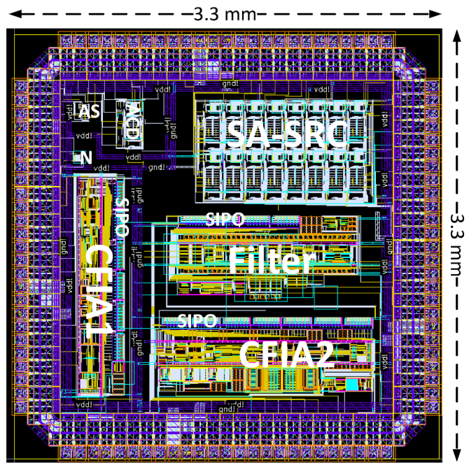
| Cell Nr. | Cell Label | Description |
|---|---|---|
| 1 | CFIA1 | CFIA circuit with manual offset calibration |
| 2 | CFIA2 | CFIA circuit with auto-digital offset autozeroing |
| 3 | Filter | Active filter circuit with non-intrusive sensors |
| 4 | SIPO | The configuration memory for the corresponding cell |
| 5 | Neuron | Modified leaky integrate-and-fire spiking model |
| 6 | Adaptive synapse | Emulated biological synapse using emulating CMOS memristor |
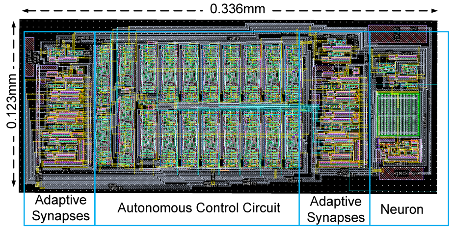
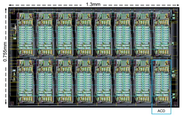
| 7 | ACD | Two adaptive synapses (AS) and one neuron (N) |
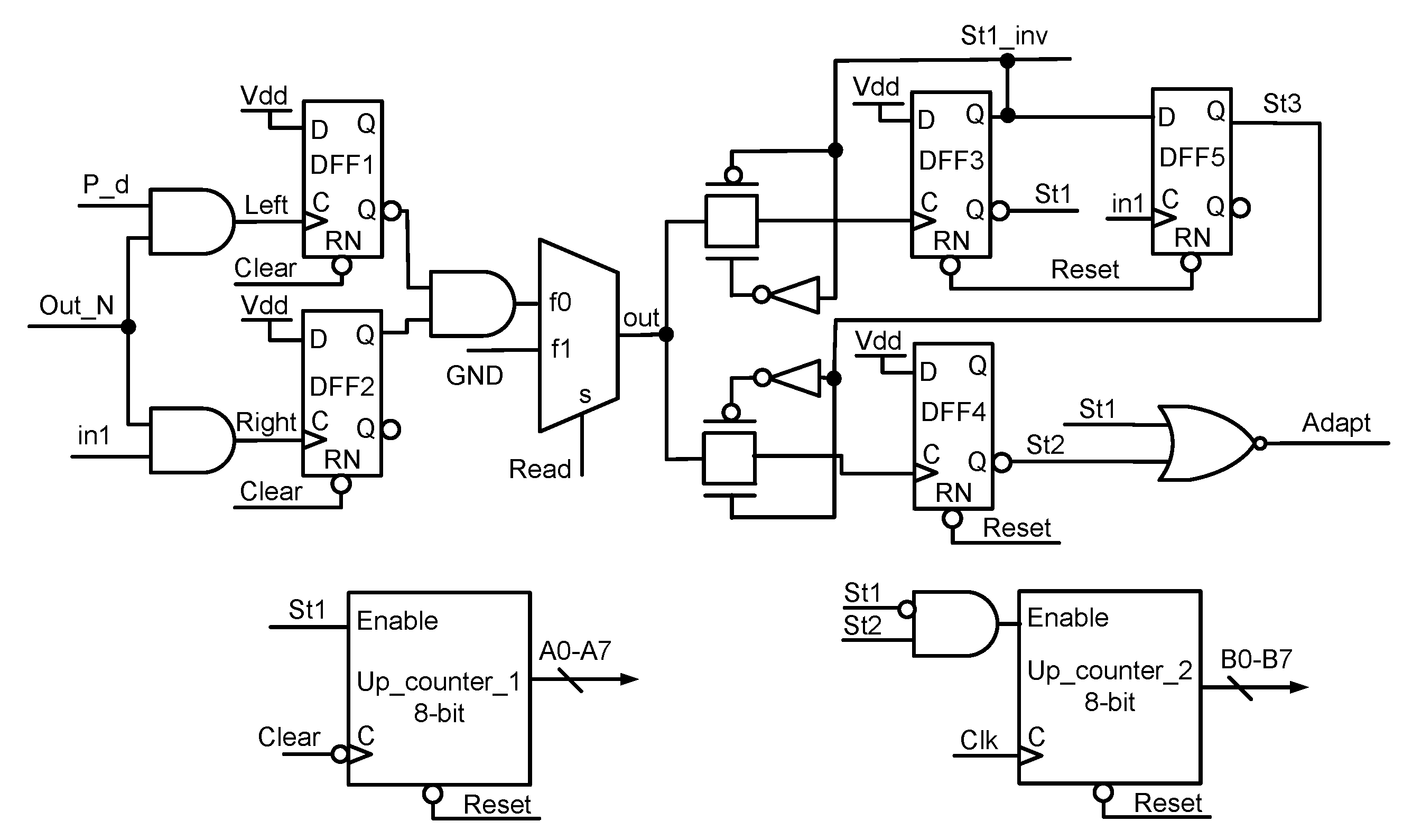
| 8 | SA-SRC | Self-adaptive spike-to-rank coding |
Publisher’s Note: MDPI stays neutral with regard to jurisdictional claims in published maps and institutional affiliations. |
© 2022 by the authors. Licensee MDPI, Basel, Switzerland. This article is an open access article distributed under the terms and conditions of the Creative Commons Attribution (CC BY) license (https://creativecommons.org/licenses/by/4.0/).
Share and Cite
Alraho, S.; Zaman, Q.; Abd, H.; König, A. Integrated Sensor Electronic Front-Ends with Self-X Capabilities. Chips 2022, 1, 83-120. https://doi.org/10.3390/chips1020008
Alraho S, Zaman Q, Abd H, König A. Integrated Sensor Electronic Front-Ends with Self-X Capabilities. Chips. 2022; 1(2):83-120. https://doi.org/10.3390/chips1020008
Chicago/Turabian StyleAlraho, Senan, Qummar Zaman, Hamam Abd, and Andreas König. 2022. "Integrated Sensor Electronic Front-Ends with Self-X Capabilities" Chips 1, no. 2: 83-120. https://doi.org/10.3390/chips1020008