Article

Signal Amplification by Means of a Dickson Charge Pump: Analysis and Experimental Validation

Dipartimento di Ingegneria Elettrica Elettronica e Informatica (DIEEI), University of Catania, I-95125 Catania, Italy
*
Author to whom correspondence should be addressed.
Chips 2022, 1(2), 72-82; https://doi.org/10.3390/chips1020007
Submission received: 15 June 2022 / Revised: 12 July 2022 / Accepted: 15 July 2022 / Published: 18 July 2022

Abstract

:
Recently, with the aim of extending the use of the CP in all those applications where a time-variant signal must be amplified with its DC component above the positive power supply rail, the signal amplification feature of a conventional Dickson charge pump (CP) has been investigated, introducing a small-signal model for each particular condition in which a CP can work. In this paper this idea is further investigated, especially under the slow switching limit (SSL) condition, and experimental validation has been carried out using a 65 nm CMOS technology for four different voltage gain values. Starting from an equivalent model of the CP, the main small- and large-signal parameters are analytically derived and discussed in depth. As a proof of concept, experimental measurements on four CPs with different numbers of stages confirm the validity of this unconventional application and the effectiveness of the CP when used as an amplifier.

1. Introduction

Since the first monolithic implementation [1], charge pumps (CPs) have been employed for on-chip generation of voltages that stay within the supply rails, behaving as a buck converter, or can reach a level off the supply rails, acting like a booster converter or a negative voltage generator [2,3,4]. The first integrated CP, the Dickson one [1], targeted the generation of the high voltages necessary to write or erase data, typically 30–40 V, in the nonvolatile memory circuits. Successively, other topologies, such as the Fibonacci, the serial-to-parallel and the exponential [5,6,7,8,9,10], as well as different design optimization strategies and ameliorative solutions of the Dickson CP have been introduced in the literature to cope with the relentless evolution of the applications.
In particular, detailed behavioral models of Dickson CP with an arbitrary number of stages were introduced in [11,12] and recently revised in [13] by using an all-resistor equivalent model in order to enrich the know-how about these blocks. Design strategies as a function of the output capacitive load were proposed in [14,15,16] with the goal to speed-up the CP and decrease output voltage ripple in low-output current applications. In [17], the suggested design strategy aimed to decrease switching power losses and increase the power conversion efficiency, and a topology based on this strategy was introduced in [18] targeting solid-state memories.
More recently, CP solutions for different types of input sources have been studied and presented. For example, in [19], a charge pump system for a flexible thermoelectric generator (TEG) with high-output impedance was described. In this case, despite the high-output impedance of the used TEG, the system controls the input voltage to keep it higher than the minimum operating voltage by modulating the input impedance of the charge pump using two-phase operation with low- and high-input impedance modes.
Dickson-based CP topologies for energy harvesting, able to be coupled with very-low voltage generators, such as TEGs, are also now an established hot topic. See, for example, [20,21], where the topologies presented enable low-voltage operation while maintaining good output current drivability.
Compared to other topologies, the Dickson CP is the least sensitive to parasitic effects and shows the smallest total capacitor area and the highest power efficiency. Therefore, the Dickson CP is the best option for integration and has become the widest adopted and studied topology. Indeed, nowadays CPs are generally used in power management units (PMUs) for an extended variety of ICs, such as the energy-autonomous nodes for the Internet of Things (IoT) and the Internet of Medical Things (IoMT), or the powered platform for the lab-on-a-chip paradigm [6,10,22,23].
Despite the huge recent growth of the number of works dealing with CPs [10], only very few of them exploit these circuits in atypical applications. Among these, in [24,25] a time-mode flash ADC exploits CPs as a part of the variable-slope voltage-to-time converter, enabling fast conversion thanks to the inherent voltage boosting operation of the CP. Another application involves CPs to re-distribute the charge inside strings of solar cells to reduce mismatches and shading effects [26,27]. Moreover, NMOS LDOs can take advantage of CP circuits to achieve low line and load sensitivities while keeping good performance in terms of drop-out voltage [28].
With the aim of extending the use of the CP in all those applications where a time-variant signal must be amplified with its DC component above the positive power supply rail, recently the authors presented the original idea to use the CP as a signal amplifier; as a preliminary proof of concept, the idea was tested for only one voltage gain value, about equal to five (i.e., only four stages) and by using an almost old 130 nm CMOS technology [29].
In this paper the novel and unconventional idea to use a CP as a signal amplifier is expanded in terms of further investigation under the slow switching limit (SSL) condition. Moreover, a wider experimental validation is carried out by using a 65 nm CMOS technology (a more scaled technology than the one in [29]) since CPs for four different voltage gains are designed and tested. In particular, four Dickson CPs, which differ for the number of stages, are designed with a 65 nm CMOS technology and experimentally tested. The behavior of the CP as an amplifier is analyzed using an equivalent model through which equations for the main design specifications are carried out and the analytical description and the developed model find a high level of agreement with the experimental results.
The paper is organized as follows. In Section 2, after some general considerations, the DC behavior of CP is exploited to introduce the small-signal equivalent model under the SSL condition. In particular, each parameter is derived and used to give the required information on both the small- and the large-signal CP performances. In Section 3, the transistor-level implementation of a proof-of-concept is analyzed, and the experimental setup together with the obtained results are reported and extensively discussed. Finally, in Section 4 concluding remarks are given.

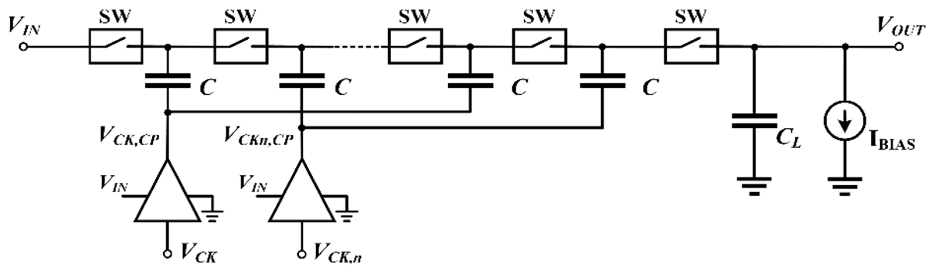
2. The Equivalent Model of the CP

2.1. General Considerations

Let us consider the simplified schematic of a Dickson CP as shown in Figure 1. Each switch allows the one-directional transfer of the charge from the input to the output, and it can be implemented using different circuit topologies, as diodes, diode-connected transistors, or active switches involving more than one transistor, such as the cross-coupled topology [10]. Each stage of the CP is made up by a switch and a pumping capacitor, C, whose value is assumed to be constant. Finally, the output block comprises a capacitor, CL, which also models the input capacitance of the circuits driven by the CP, and a bias current generator, IBIAS, which sets the quiescent point of the CP with the DC input voltage.
It is worth noting that in Figure 1, unlike the conventional CP scheme, the input voltage, VIN, is connected also to the buffers driving the pumping capacitors. Adopting this solution, the digital buffers behaves as a two-input MUX and the output signals, VCK,CP(t) and VCKn,CP(t), are then given by
V C K , C P ( t ) = V I N ( t ) Π ( t T S )
V C K n , C P ( t ) = V I N ( t ) Π ( t T S + 1 2 )
where the canonical function Π(t/Ts) represents a square wave with a period equal to Ts and high and low level equal to 1 and 0, respectively.
Note that the minimum and maximum VIN,DC values depends on the adopted technology. Indeed, they are fixed by the breakdown voltage of both the capacitors and the transistors, which limits the maximum value, and the device’s threshold voltage, which determines the input minimum value.
Similarly to the study of a traditional amplifier, the input signal can be split into the DC and AC components, VIN,DC and vin,ac(t), respectively, whose relationship satisfies the small signal condition (i.e., vin,ac << VIN,DC).

2.2. DC Behavior

As shown in [5], considering the DC component of the input signal only, the CP in Figure 1 can be modeled using the equivalent circuit shown in Figure 2, whose output voltage DC component is VOUT,DC. The input current source, IIN,SW, models the switching losses due to the stray capacitance of the stage capacitors, and is expressed by
I I N , S W = 0.5 N ( C B + C T ) f S V I N
where CB and CT are the bottom and top parasitic capacitance of each pumping capacitor, respectively.
When the clock period is high enough to allow the complete charge transfer from one stage to the following one, the CP works in the slow switching limit (SSL) [5]. In this condition, the output resistance can be expressed by
R O U T = N ( 1 + α ) C f s
where N is the number of stages and the factor α is the ratio between the top parasitic capacitance and the nominal value of the stage capacitance.
The ideal transformer in Figure 2 models the voltage gain, which is the main outcome of the charge pumping mechanism. Therefore, by analyzing the circuit in Figure 2, the VOUT,DC is analytically given by
V O U T , D C = ( N 1 + α + 1 ) V I N , D C R O U T I B I A S

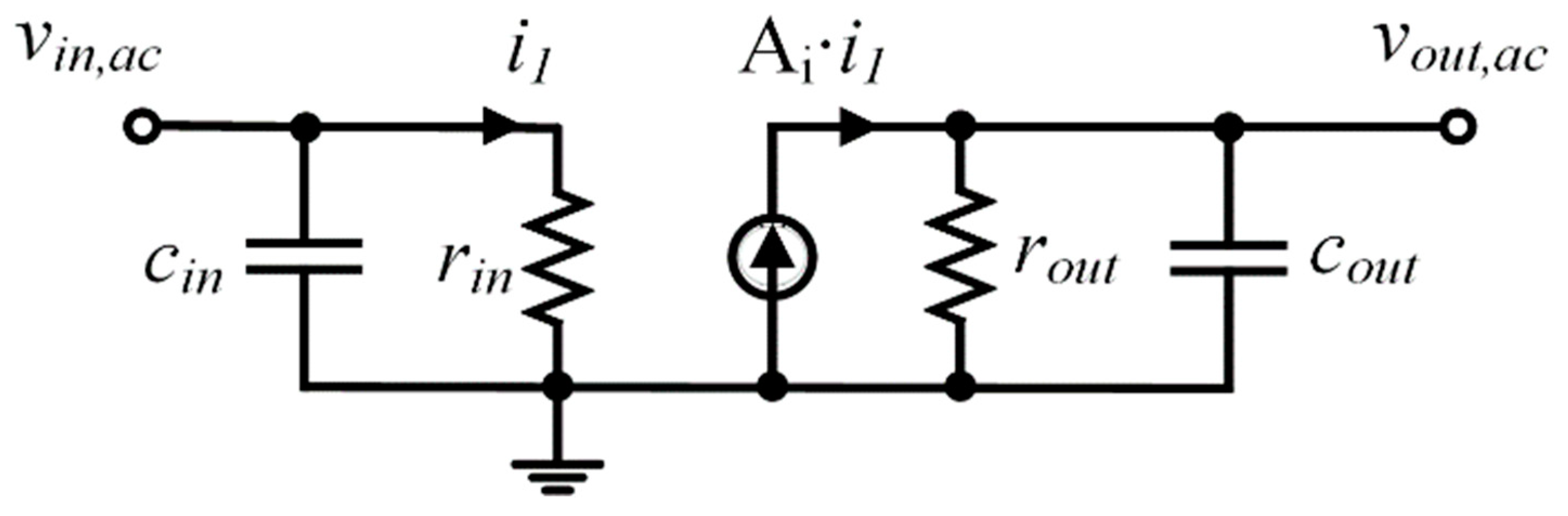
2.3. AC Behavior in SSL

Without loss of consistence, in the analysis to come we neglect the on-resistance of the PMOS (i.e., the pull up network) of the buffers. Indeed, in practical cases such resistance can be made negligible by sizing the transistors of the buffers opportunely large. (This design strategy is conventionally adopted for CP-based on-chip voltage generation. However, for the MOSFETs of the buffers involved in the path of all CP currents, their on-resistances increase the total equivalent resistance seen by the pumping capacitors. Thus, the width of the SSL domain is reduced and, equivalently, the CP is pushed to go to and enter into the FSL domain. However, in such a case, the model to be used is another one (see ref. [29]).) Moreover, assuming the adoption of non-overlapping clock signals, we also neglect the short circuit currents of the buffers. In addition, we assume that the reverse current of the switches is negligible. Finally, we suppose that the output capacitive load, CL, is small enough in comparison to the CP pumping capacitance that its effect can be initially neglected.
Under the SSL condition, the Dickson CP in Figure 1 can be modeled through the small-signal equivalent circuit shown in Figure 3.
Parameters cin and rin model the input impedance of the CP. In particular, from Figure 3, the capacitance cin corresponds to the total capacitive load of the buffers (i.e., the total parasitic bottom plate capacitance); thus,
c i n = N C B
Considering that in the SSL the CP can be supposed to work like a switched-capacitor (SC) circuit, and remembering that the SC small-signal resistance is proportional to TS/C [5], for a series of N stages we can write
r o u t = N ( 1 + α ) C f S
Neglecting losses, from Figure 2 the input power is equal to the output power; thus, we can write
r i n = r o u t ( i o u t i i n ) 2 = N [ N 1 + α + 1 ] 2 1 ( 1 + α ) C f S
To analyze how the CP transports the total input current through the different stages up to the output node, let us consider a Gaussian curve around the CP. Applying Kirchhoff’s current law in steady-state, the total current flowing into the CP is equal to (N/(1 + α) + 1)-times the one that flows out during each clock period. Consequently, the current gain, Ai, of the current-controlled current source generator is equal to 1/(N/(1 + α) + 1).
Finally, the CP small signal output capacitance is expressed by
c o u t = A ( N ) N ( 1 + α ) C
whose values coincides with the switching impedance of the pumping capacitors and, thus, to the CP self-capacitance [12]. The function A(N) was introduced in [12] and its value is reported here as
A ( N ) = N ( 4 N 2 + 3 N + 2 ) 12 ( N + 1 ) ,   for   even   N
A ( N ) = 4 N 2 N 3 12 ,   for   odd   N
The output impedance introduces an intrinsic pole which defines the bandwidth of the CP. Hence, the CP transfer function can be expressed as
H C P ( s ) = N 1 + α + 1 1 + s ω P i
where the intrinsic pole frequency, ωPi, is given by
ω P i = 1 A ( N ) f S
The intrinsic pole in (13) depends on the clock frequency, fS, and approaches the value 3fS/N2 for N > 4. Considering the CP capacitive extrinsic load, CL, the resulting pole frequency is given by
ω P = 1 r o u t ( C L + c o u t ) C N C L f S
where the rightmost approximation holds when CL is greater than the CP self-capacitance expressed in (9). From (14), ωP is inversely proportional to the number of stages, N, whereas the intrinsic pole, ωPi, is inversely proportional to N2.

2.4. Small- and Large-Signal Analysis

A simplified expression of the intrinsic gain-bandwidth product (GBW) can be defined for a CP considering the ideal gain, N/(1 + α) + 1, and the bandwidth fixed by the pole frequency derived in the previous section, thus yielding
G B W = N 1 + α + 1 2 π r o u t ( C L + c o u t )
A key amplifier parameter for large-signal behavior is the slew rate (SR). In a CP used as a single-stage amplifier, the SR is limited by the maximum charging/discharging current provided by the charge transfer mechanism. Thus, considering that the charge level of the output capacitor can be changed by the input current and the bias current only, the SR can be expressed as
S R min [ I B I A S C L + c o u t , v o u t , a c r o u t ( C L + c o u t ) ]
Note that since IBIAS/(CL + cout) or vout,ac/rout(CL + cout) is proportional to the gain-bandwidth product, an increase of the GBW generates a proportional increase of the SR.

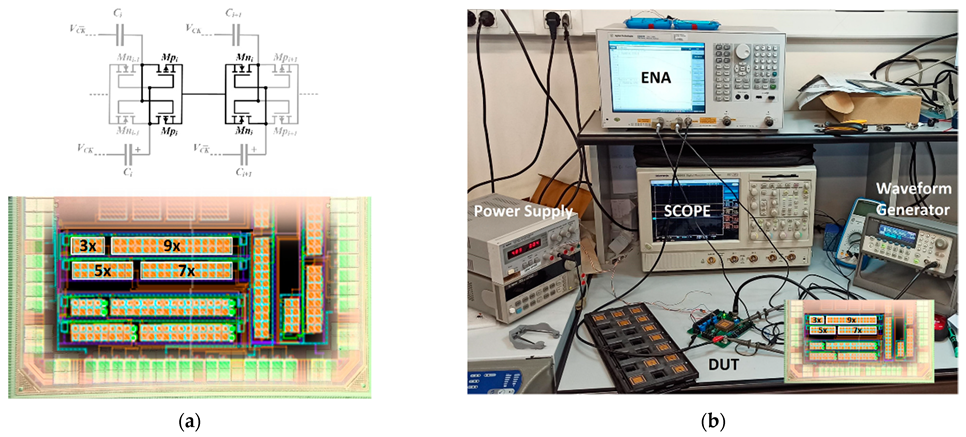
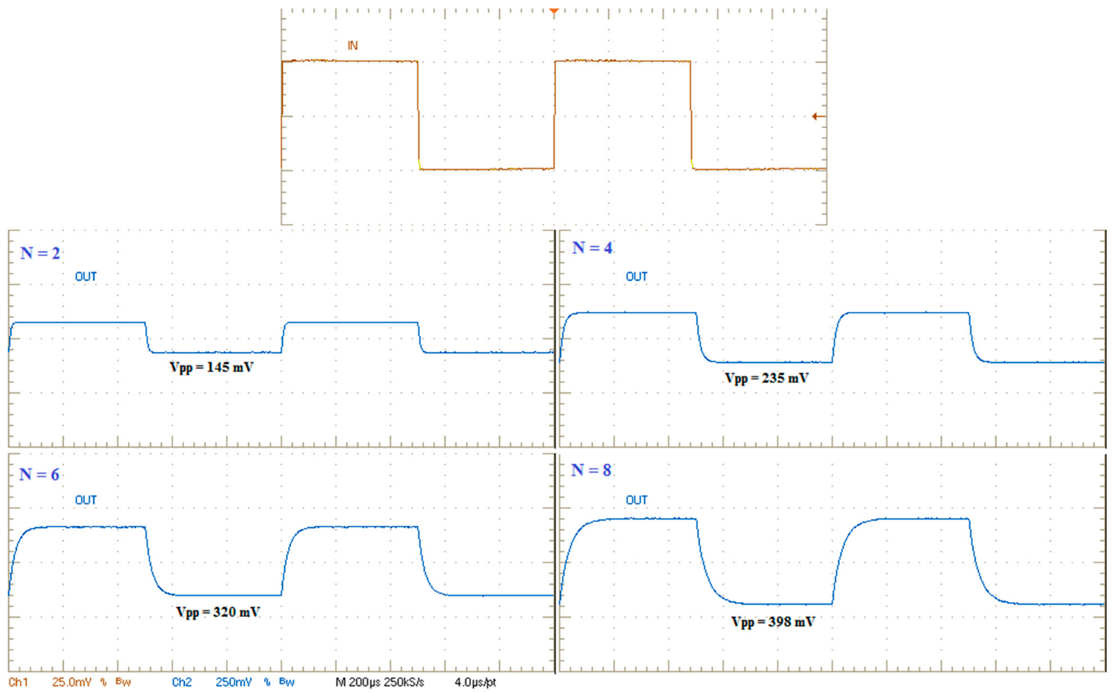
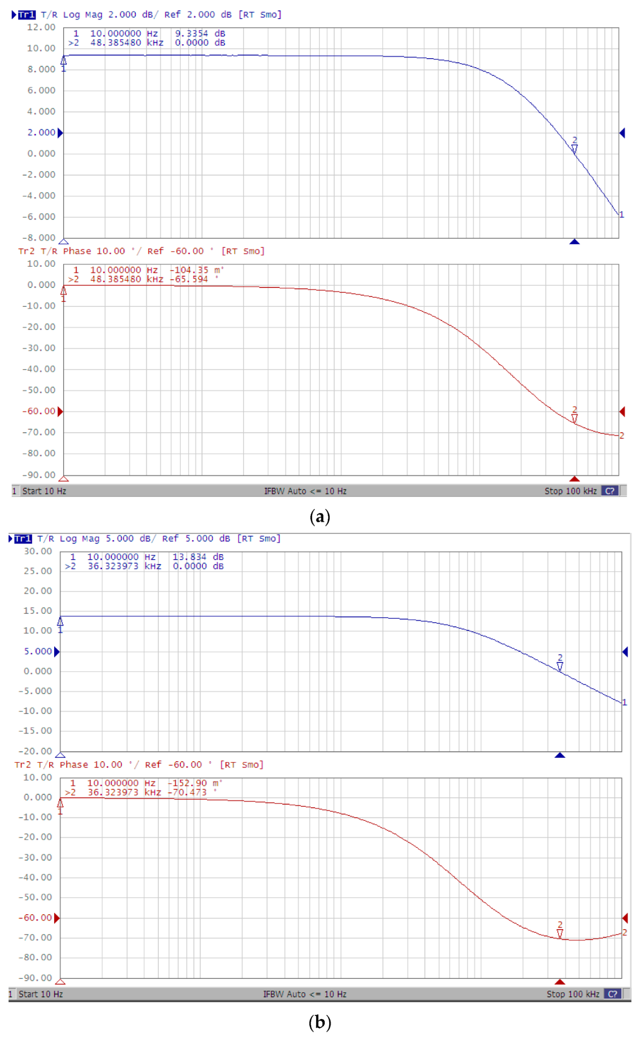
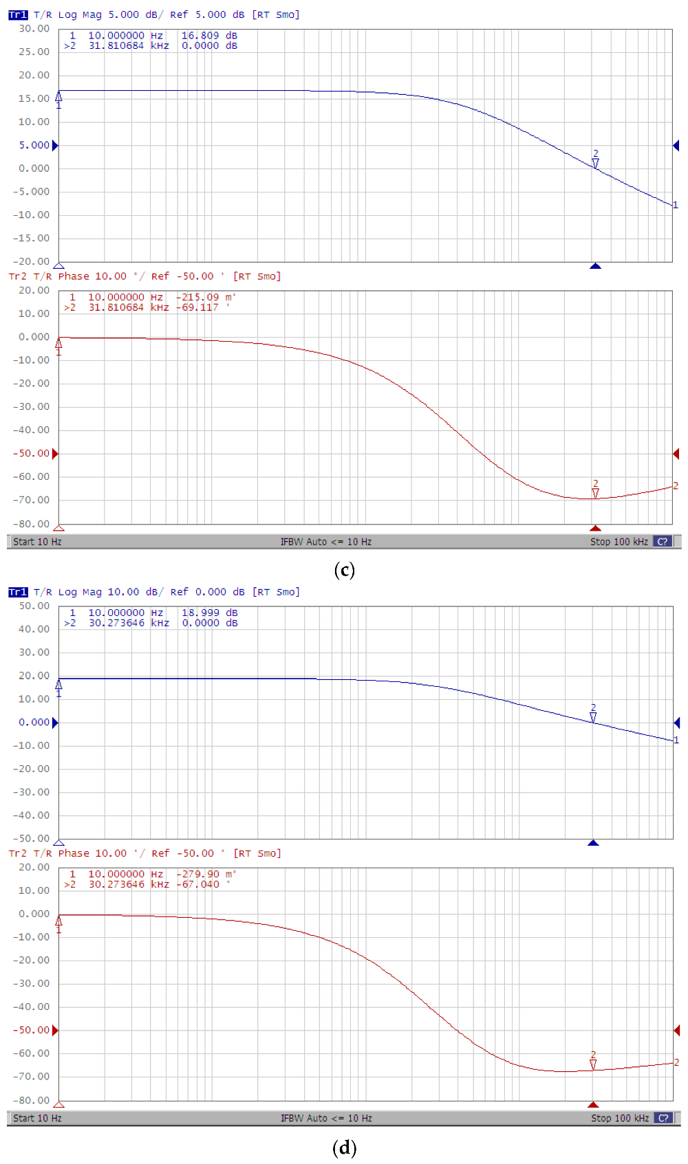
3. Experimental Validation

To verify the behavior of the unconventional use of the CP as a signal amplifier and validate the analytical model derived, four CPs with different numbers of stages (namely N = 2, 4, 6 and 8 with nominal gain equal to 3×, 5×, 7× and 9×, respectively) were implemented using the 65 nm triple-well CMOS technology provided by STMicroelectronics. Figure 4a shows the schematic of the adopted switch which is referred to as dual-branch cross-coupled topology (also named “latched”) [30,31,32]. The bottom of Figure 4a shows the layout of the CPs superimposed over the chip microphotograph. The occupied area is 56 × 101 µm2, 56 × 220 µm2, 56 × 330 µm2 and 56 × 440 µm2 for the 2-, 4-, 6- and 8-stage CP, respectively.
Design constraints have been set as f = 1 MHz, IBIAS = 0.1 µA and VIN,DC = 300 mV. The value of the pumping capacitances is C = 10 pF and they are implemented with MIM technology, which provides high specific capacity and low top stray capacitance (α = 0.04). The NMOS and PMOS transistors all have a 0.1 µm channel length and an aspect ratio equal to 100. The clock buffers are opportunely sized to not affect the CP responses. In particular, they are implemented by using conventional CMOS inverters whose aspect ratios of PMOS and NMOS transistors are 100 and 200, respectively, with a channel length equal to 60 nm. Finally, an external capacitance equal to 50 pF is connected at the output of each CP (comprising the capacitive contributions of the oscilloscope probe, package and PCB connections, with an externally added capacitor to reach the accurate value).
Figure 4b shows the experimental setup involving an oscilloscope, a power supply for input voltage supplement, a waveform generator and a network analyzer (ENA) to allow transient and AC measurements. The PCB prototype hosts the test chip (DUT). All the circuits have been characterized for small- and large-signal response over 10 samples.
Figure 5 shows the transient output of the CPs in the SSL for a 500 Hz, 50 mV input square wave. The voltage gain is equal to 2.9, 4.7, 6.4 and 7.96 for the 2-, 4-, 6- and 8-stage CP, respectively.
The value of the gain is confirmed in Figure 6, which reports the measured frequency response of the same samples. From this figure it is apparent that the CPs behave like a single-pole system with a GBW equal to 48.38 kHz, 36.32 kHz, 31.81 kHz and 30.27 kHz for the 2-, 4-, 6- and 8-stage CP, respectively.
Table 1 summarizes the transient and frequency response measurement results over 10 samples. As can be verified, the results agree with the analytical prediction with an accuracy error always lower than 14%. The results found are in agreement and further confirm the preliminary experimental results reported in [29], but obtained with an older CMOS technology and for only the case of a voltage gain equal to about 4. In other words, with much more confidence and generality we can confirm the validity of the use of a Dickson CP as signal amplifier and the accuracy of the model derived.

4. Conclusions

This work discusses the use of the Dickson CP as a signal amplifier and explores its time and frequency domain characteristics. The analytical equations and the main design metrics commonly used to evaluate the performance of a conventional amplifier are derived using a simple while accurate equivalent model of the CP working in the slow switching limit. The results obtained through measurements on four CPs, implemented in a 65 nm CMOS technology, confirm the validity of the proposed idea. It is worth noting, however, that the CP cannot be considered as a substitute of conventional amplifiers, but it can be profitably exploited in all those applications where a signal superimposed to a DC component higher than the power supply voltage is required, such as drivers for piezoelectric devices for ultrasound imaging, NMOS LDOs or implanted biomedical devices powered and communicating using single solar cells. Finally, it is worth noting that the proposed model can be extended to other CP topologies which may show an inherent higher GBW but at the cost of lower efficiency and area occupation.

Author Contributions

Conceptualization, A.B.; data curation, A.B. and A.D.G.; writing—original draft preparation, A.B.; writing—review and editing, A.B. and A.D.G.; formal analysis, all authors; supervision, G.P. and A.D.G. All authors have read and agreed to the published version of the manuscript.

Funding

This work was supported by the Piano di incentivi per la ricerca di Ateneo 2020/2022 (Pia.ce.ri) Linea 2D—University of Catania.

Institutional Review Board Statement

Not applicable.

Informed Consent Statement

Not applicable.

Data Availability Statement

Not applicable.

Conflicts of Interest

The authors declare no conflict of interest.

References

  1. Dickson, J. On-chip high-voltage generation in MNOS integrated circuits using an improved voltage multiplier technique. IEEE J. Solid-State Circuits 1976, 11, 374–378. [Google Scholar] [CrossRef]
  2. Fan, S.; Dong, J.; Zhang, R.; Xue, Z.; Geng, L. A reconfigurable multi-ratio charge pump with wide input/output voltage range for wireless energy harvesting system. In Proceedings of the 2018 IEEE MTT-S International Wireless Symposium (IWS), Chengdu, China, 6–10 May 2018; pp. 1–3. [Google Scholar] [CrossRef]
  3. Pulvirenti, F. 3-V Input, 70-V Output, Fully Integrated Hybrid Charge Pump. IEEE Access 2022, 10, 44062–44075. [Google Scholar] [CrossRef]
  4. Tan, Y.; Zhan, C.; Wang, G. A Fully-On-Chip Analog Low-Dropout Regulator with Negative Charge Pump for Low-Voltage Applications. IEEE Trans. Circuits Syst. II Express Briefs 2019, 66, 1361–1365. [Google Scholar] [CrossRef]
  5. Seeman, M.D.; Sanders, S.R. Analysis and Optimization of Switched-Capacitor DC–DC Converters. IEEE Trans. Power Electron. 2008, 23, 841–851. [Google Scholar] [CrossRef]
  6. Ballo, A.; Grasso, A.D.; Palumbo, G. A Review of Charge Pump Topologies for the Power Management of IoT Nodes. Electronics 2019, 8, 480. [Google Scholar] [CrossRef] [Green Version]
  7. Ueno, F.; Inoue, T.; Oota, I.; Harada, I. Emergency power supply for small computer systems. In Proceedings of the 1991 IEEE International Sympoisum on Circuits and Systems, Singapore, 11–14 June 1991; Volume 2, pp. 1065–1068. [Google Scholar] [CrossRef]
  8. Brugler, J. Theoretical performance of voltage multiplier circuits. IEEE J. Solid-State Circuits 1971, 6, 132–135. [Google Scholar] [CrossRef]
  9. Ker, M.-D.; Chen, S.-L.; Tsai, C.-S. Design of Charge Pump Circuit With Consideration of Gate-Oxide Reliability in Low-Voltage CMOS Processes. IEEE J. Solid-State Circuits 2006, 41, 1100–1107. [Google Scholar] [CrossRef] [Green Version]
  10. Ballo, A.; Grasso, A.D.; Palumbo, G.; Tanzawa, T. Charge Pumps for Ultra-Low-Power Applications: Analysis, Design, and New Solutions. IEEE Trans. Circuits Syst. II Express Briefs 2021, 68, 2895–2901. [Google Scholar] [CrossRef]
  11. Palumbo, G.; Barniol, N.; Bethaoui, M. Improved behavioral and design model of an Nth-order charge pump. IEEE Trans. Circuits Syst. I Regul. Pap. 2000, 47, 264–268. [Google Scholar] [CrossRef]
  12. Tanzawa, T.; Tanaka, T. A dynamic analysis of the Dickson charge pump circuit. IEEE J. Solid-State Circuits 1997, 32, 1231–1240. [Google Scholar] [CrossRef]
  13. Aloqlah, A.S.; Alhawari, M. A Resistor-Network Model of Dickson Charge Pump Using Steady-State Analysis. Energies 2022, 15, 1899. [Google Scholar] [CrossRef]
  14. Palumbo, G.; Pappalardo, D. Charge pump circuits with only capacitive loads: Optimized design. IEEE Trans. Circuits Syst. II Express Briefs 2006, 53, 128–132. [Google Scholar] [CrossRef]
  15. Ballo, A.; Grasso, A.D.; Palumbo, G.; Tanzawa, T. Linear distribution of capacitance in Dickson charge pumps to reduce rise time. Int. J. Circuit Theory Appl. 2020, 48, 555–566. [Google Scholar] [CrossRef]
  16. Lin, Y.; Yang, J.; Mui, T.-W.; Zhou, Y.; Leung, K.-N. Optimization of Charge Pump Based on Piecewise Modeling of Output-Voltage Ripple. Energies 2021, 14, 4809. [Google Scholar] [CrossRef]
  17. Ballo, A.; Grasso, A.D.; Palumbo, G. A simple and effective design strategy to increase power conversion efficiency of linear charge pumps. Int. J. Circuit Theory Appl. 2020, 48, 157–161. [Google Scholar] [CrossRef]
  18. Ballo, A.; Grasso, A.D.; Palumbo, G. A Memory-Targeted Dynamic Reconfigurable Charge Pump to Achieve a Power Consumption Reduction in IoT Nodes. IEEE Access 2021, 9, 41958–41964. [Google Scholar] [CrossRef]
  19. Koketsu, K.; Tanzawa, T. Design of a Charge Pump Circuit and System with Input Impedance Modulation for a Flexible-Type Thermoelectric Generator with High-Output Impedance. Electronics 2021, 10, 1212. [Google Scholar] [CrossRef]
  20. Ballo, A.; Grasso, A.D.; Palumbo, G. A Subthreshold Cross-Coupled Hybrid Charge Pump for 50-mV Cold-Start. IEEE Access 2020, 8, 188959–188969. [Google Scholar] [CrossRef]
  21. Yong, J.K.; Ramiah, H.; Churchill, K.K.P.; Chong, G.; Mekhilef, S.; Chen, Y.; Mak, P.-I.; Martins, R.P. A 0.1-V VIN Subthreshold 3-Stage Dual-Branch Charge Pump with 43.4% Peak Power Conversion Efficiency Using Advanced Dynamic Gate-Bias. IEEE Trans. Circuits Syst. II Express Briefs 2022, 1. [Google Scholar] [CrossRef]
  22. Potocny, M.; Kovac, M.; Arbet, D.; Sovcik, M.; Nagy, L.; Stopjakova, V.; Ravasz, R. Low-Voltage DC-DC Converter for IoT and On-Chip Energy Harvester Applications. Sensors 2021, 21, 5721. [Google Scholar] [CrossRef]
  23. Zhu, X.; Fu, Q.; Yang, R.; Zhang, Y. A High Power-Conversion-Efficiency Voltage Boost Converter with MPPT for Wireless Sensor Nodes. Sensors 2021, 21, 5447. [Google Scholar] [CrossRef] [PubMed]
  24. Esmailiyan, A.; Schembari, F.; Staszewski, R.B. A 0.36-V 5-MS/s Time-Mode Flash ADC With Dickson-Charge-Pump-Based Comparators in 28-nm CMOS. IEEE Trans. Circuits Syst. I Regul. Pap. 2020, 67, 1789–1802. [Google Scholar] [CrossRef]
  25. Esmailiyan, A.; Du, J.; Siriburanon, T.; Schembari, F.; Staszewski, R.B. Dickson-Charge-Pump-Based Voltage-to-Time Conversion for Time-Based ADCs in 28-nm CMOS. IEEE Open J. Circuits Syst. 2021, 2, 23–31. [Google Scholar] [CrossRef]
  26. Gokdag, M.; Akbaba, M.; Gulbudak, O. Switched-capacitor converter for PV modules under partial shading and mismatch conditions. Sol. Energy 2018, 170, 723–731. [Google Scholar] [CrossRef]
  27. Wang, Y.; Yan, N.; Min, H.; Shi, C.-J.R. A High-Efficiency Split–Merge Charge Pump for Solar Energy Harvesting. IEEE Trans. Circuits Syst. II Express Briefs 2017, 64, 545–549. [Google Scholar] [CrossRef]
  28. Woo, K.-C.; Yang, B.-D. A 0.35V 90nA Quiescent Current Output-Capacitor-Less NMOS Low-Dropout Regulator Using a Coarse-Fine Charge-Pump Circuit. IEEE Trans. Circuits Syst. II Express Briefs 2020, 67, 3118–3122. [Google Scholar] [CrossRef]
  29. Ballo, A.; Grasso, A.D.; Palumbo, G. The Dickson Charge Pump as a Signal Amplifier. IEEE Trans. Circuits Syst. Regul. Pap. 2022, 1–14. [Google Scholar] [CrossRef]
  30. Nakagome, Y.; Tanaka, H.; Takeuchi, K.; Kume, E.; Watanabe, Y.; Kaga, T.; Kawamoto, Y.; Murai, F.; Izawa, R.; Hisamoto, D.; et al. An experimental 1.5-V 64-Mb DRAM. IEEE J. Solid-State Circuits 1991, 26, 465–472. [Google Scholar] [CrossRef]
  31. Gariboldi, R.; Pulvirenti, F. A monolithic quad line driver for industrial applications. IEEE J. Solid-State Circuits 1994, 29, 957–962. [Google Scholar] [CrossRef]
  32. Gariboldi, R.; Pulvirenti, F. A 70 mΩ Intelligent High Side Switch with Full Diagnostics. In Proceedings of the ESSCIRC ’95: Twenty-first European Solid-State Circuits Conference, Lille, France, 19–21 September 1995; pp. 262–265. [Google Scholar]
Figure 1. Simplified schematic of a Dickson charge pump.
Chips 01 00007 g001
Figure 2. Equivalent static model of the CP.
Chips 01 00007 g002
Figure 3. Small signal equivalent model of the CP working in SSL.
Chips 01 00007 g003
Figure 4. (a) Simplified circuit diagram of a stage of the CP (top) and layouts of the CPs superimposed on the chip photo (bottom); (b) experimental setup.
Chips 01 00007 g004
Figure 5. Measured transient responses to a 50 mVpp square-wave input signal.
Chips 01 00007 g005
Figure 6. Measured frequency response of the CP for N = (a) 2; (b) 4; (c) 6; and (d) 8.
Chips 01 00007 g006aChips 01 00007 g006b
Table 1. Measured charge pumps parameters over 10 samples @ CL = 50 pF.
Parameter2-Stage CP4-Stage CP6-Stage CP8-Stage CP
μ/σModelεP2M%μ/σModelεP2M%μ/σModelεP2M%μ/σModelεP2M%
UGF (kHz)41.3/1.343.5−5.333.6/1.234−1.130.3/0.929.91.528.8/0.527.25.6
DC gain (dB)9.28/0.079.32−0.413.71/0.1313.710.0216.63/0.1416.610.118.81/0.1418.780.2
Settling time a (ms)0.34/0.020.319.10.68/0.030.663.51.14/0.061.048.51.56/0.081.475.8
SR a (V/ms)15.75/0.1913.6713.211.26/0.1510.675.210.35/0.089.389.49.12/0.118.556.3
a Average between positive and negative values; “εP2M%”—predicted to average measure relative error (accuracy).
Publisher’s Note: MDPI stays neutral with regard to jurisdictional claims in published maps and institutional affiliations.

