
Advances on Sb2Se3 Solar Cells Fabricated by Physical Vapor Deposition Techniques


Abstract
:
1. Introduction
- Short carrier lifetime: The carrier lifetime is the average time that a charge carrier (electron or hole) can exist before it recombines with another carrier. The short carrier lifetime in Sb2Se3 is due to the high density of defects, such as Se vacancies and SbSe/SeSb antisite defects [9].
- Low hole density: The hole density is the number of holes per unit volume in a semiconductor material. The low hole density in intrinsic Sb2Se3 is another factor that limits the efficiency of the solar cells [2].
- Lack of suitable hole and electron transport layer materials: The hole transport layer (HTL) and electron transport layer (ETL) are the materials that transport the holes and electrons, respectively, to the respective electrodes of the solar cell. The lack of suitable HTL and ETL materials is also a challenge for the development of high-efficiency Sb2Se3 solar cells [10].
2. Physical Vapor Deposition Techniques for Planar-Type Structure Sb2Se3 Solar Cells
- A transparent electrode layer or metal grid (Al or Au)
- A window layer (for example undoped ZnO)
- An ETL (for example CdS)
- An Sb2Se3 absorber layer
- An HTL
- A metallic or conductive oxide back-contact
- A glass substrate.
- A metal contact
- An HTL (for example Spiro-MeOTAD, P3HT, NiOx)
- An Sb2Se3 absorber layer
- An ETL (for example TiO2 or CdS)
- A transparent conductive oxide
- Glass (substrate).
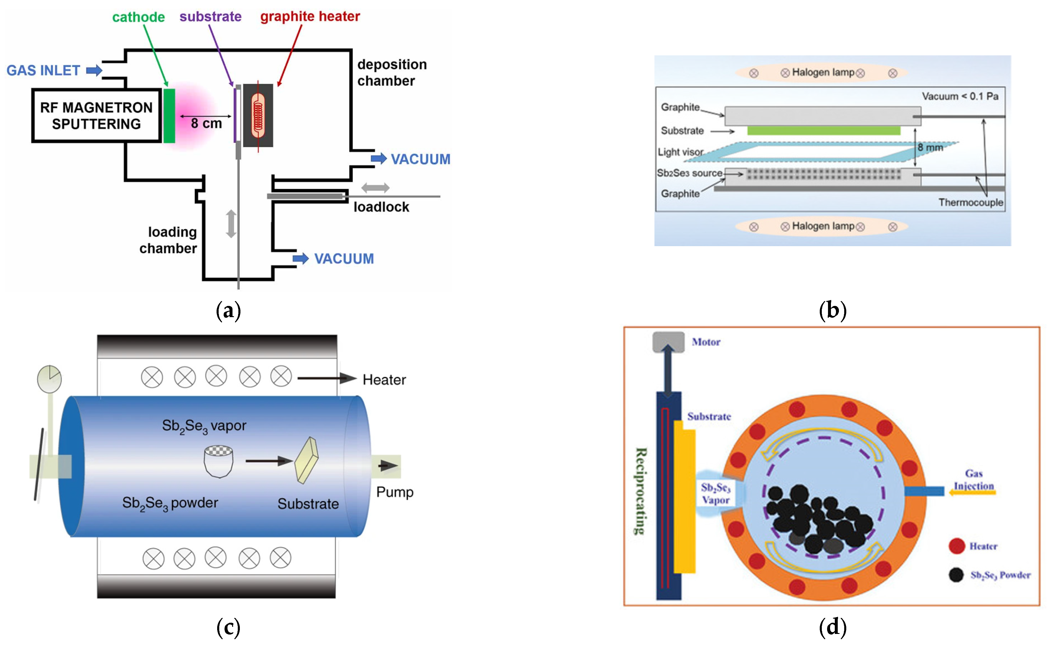
- Magnetron sputtering;
- Close-spaced sublimation (CSS);
- Rapid thermal evaporation (RTE);
- Vapor transport deposition (VTD);
- Injected vapor deposition (IVT);
- Pulsed laser deposition (PLD);
- Pulsed electron deposition (PED).
2.1. Magnetron Sputtering
2.2. Close-Spaced Sublimation
2.3. Rapid Thermal Evaporation
2.4. Vapor Transport Deposition
2.5. Injected Vapor Deposition
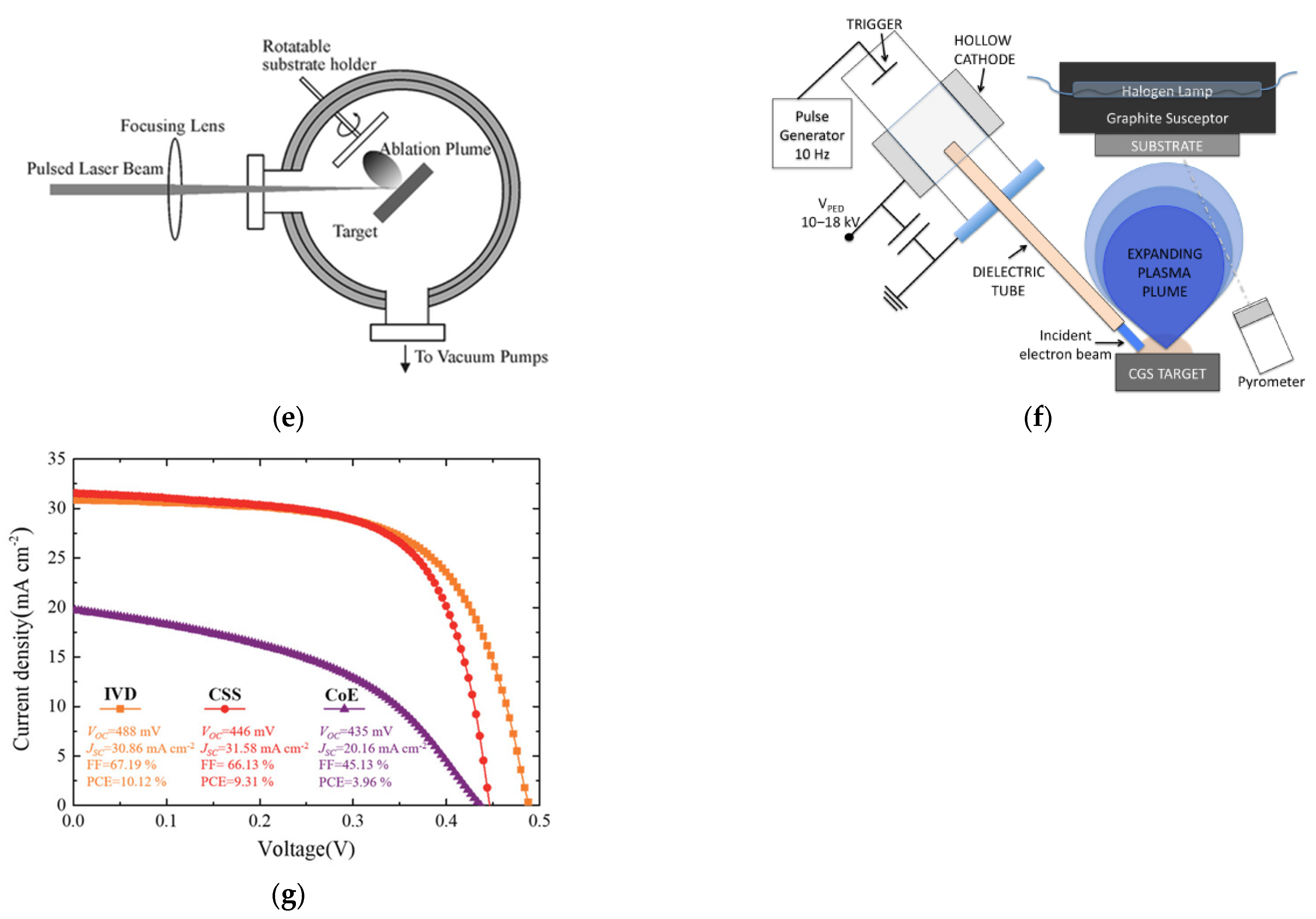
2.6. Pulsed Laser Deposition
2.7. Pulsed Electron Deposition


3. The Main Challenges for Sb2Se3—Based Solar Cells (1D-Ribbon Alignment, HTL/ETL, Interfacial Engineering and Band Alignment, Doping)
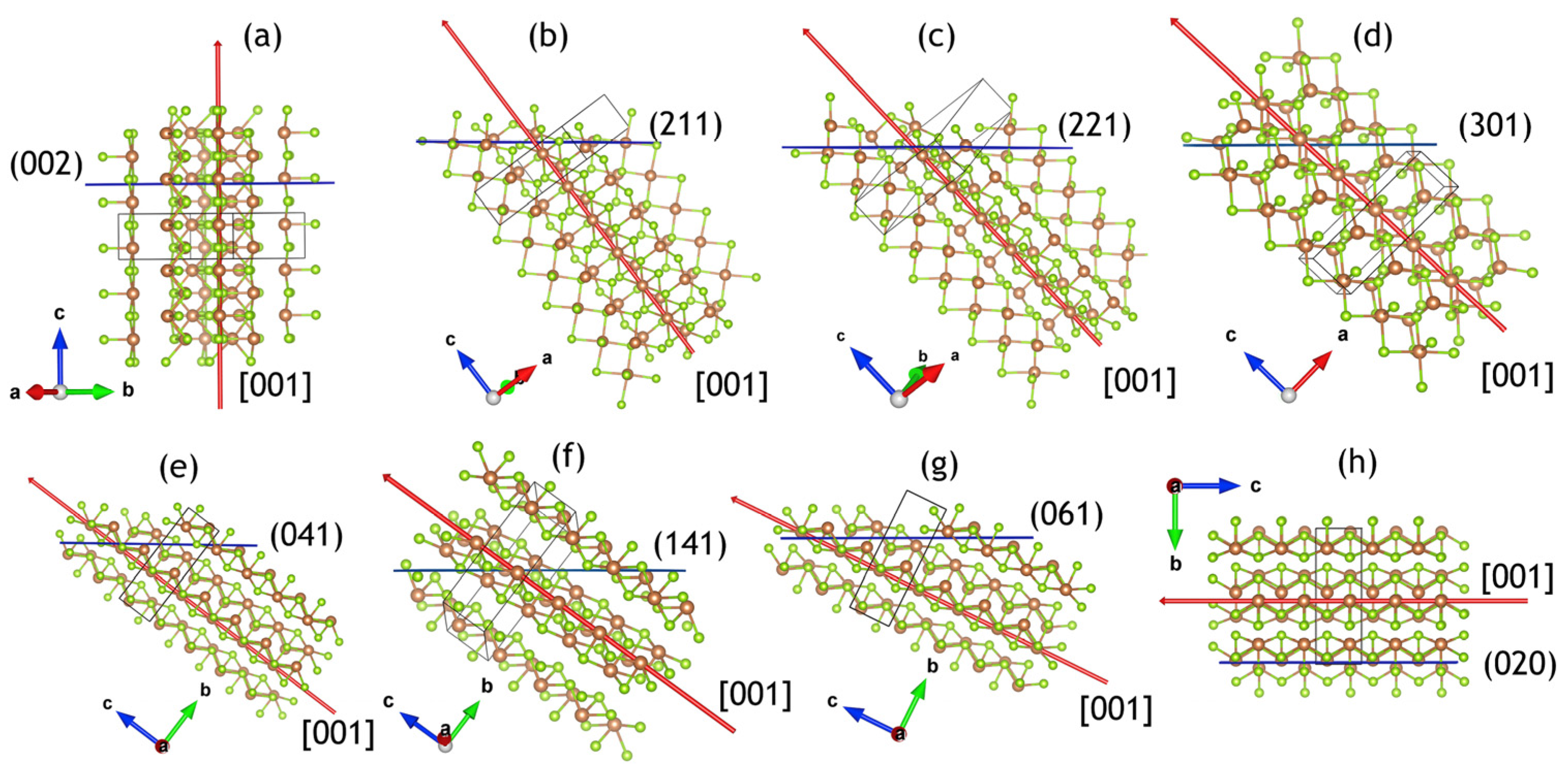
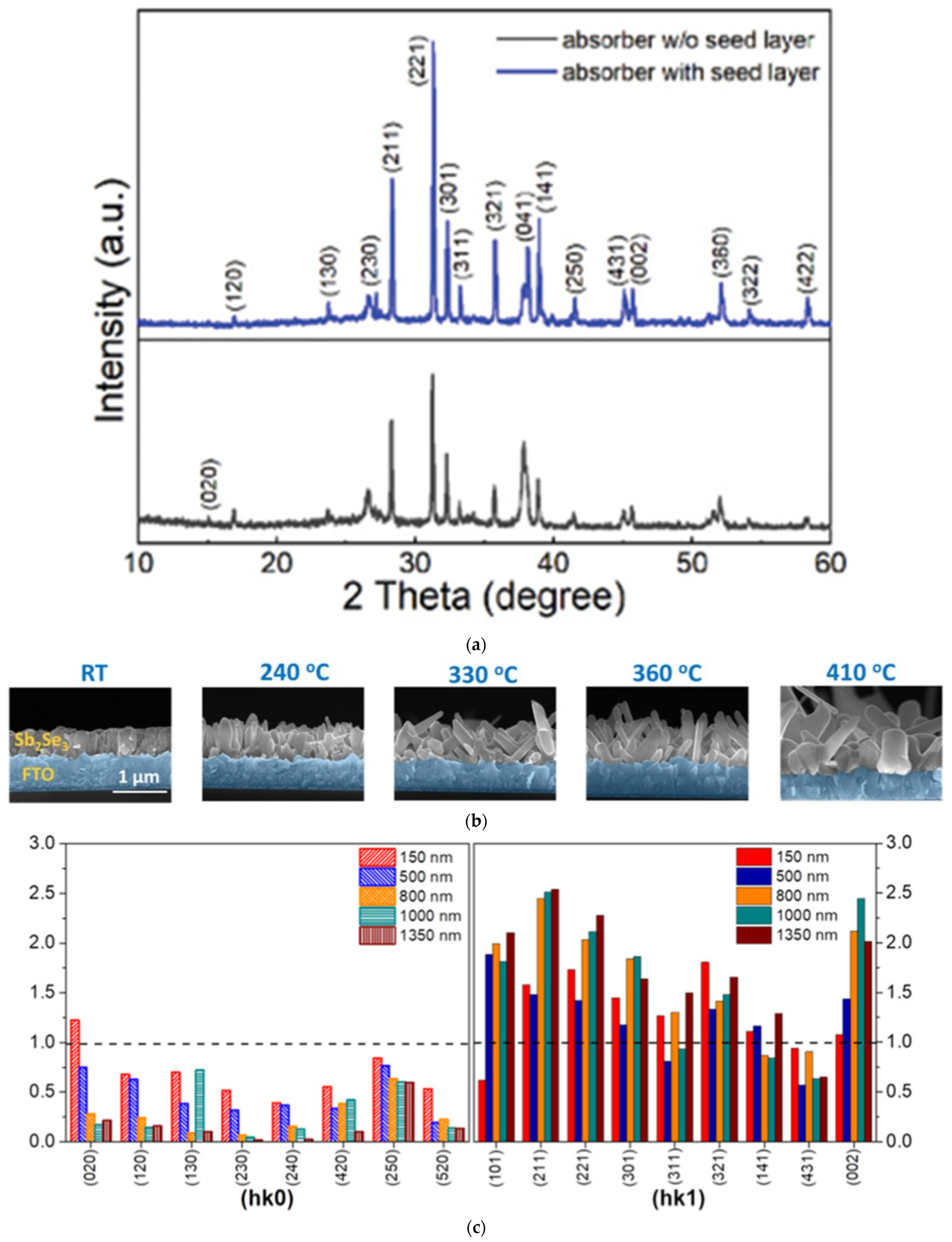
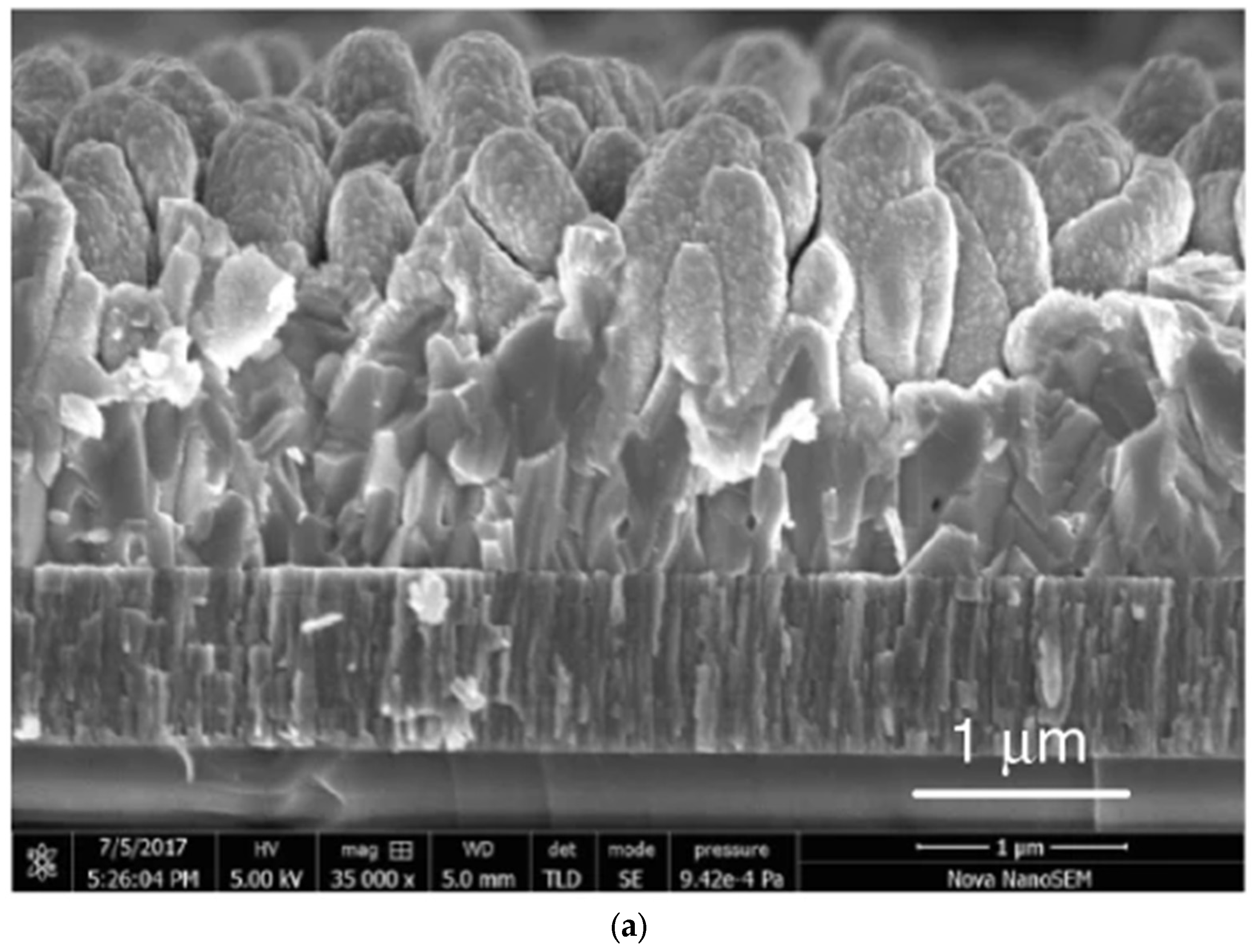
3.1. One-Dimensional-Ribbon Alignment
3.2. HTL/ETL, Interfacial Engineering, and Band Alignment
3.2.1. ETLs
3.2.2. HTLs
3.3. Doping
4. Conclusions
Author Contributions
Funding
Institutional Review Board Statement
Informed Consent Statement
Data Availability Statement
Acknowledgments
Conflicts of Interest
Nomenclature
| Ag | Silver |
| AgSbSe2 | Silver antimony selenide |
| Al | Aluminum |
| Al2O3 | Aluminum(III) oxide |
| ALD | Atomic layer deposition |
| Alq3 | Tris(8-hydroxyquinolinato)aluminum, Al(C9H6NO)3 |
| Ar | Argon |
| Au | Gold |
| AZO | Aluminum-doped zinc oxide |
| C60 | Buckminsterfullerene |
| CBD | Chemical bath deposition |
| CBO | Conduction band offset |
| Cd | Cadmium |
| CdCl2 | Cadmium chloride |
| CdS | Cadmium sulfide |
| CdS:O | Oxygenated cadmium sulfide |
| CdTe | Cadmium telluride |
| CdZnS | Cadmium zinc sulfide |
| CeO2 | Cerium(IV) oxide |
| CIGS, Cu(In,Ga)Se2 | Copper indium gallium (di)selenide |
| CIGSSe | Copper indium gallium sulfur selenide |
| CSS | Close-space sublimation |
| CuI | Copper(I) iodide |
| CuInSe2 | Copper indium selenide |
| CuSbSe2 | Copper antimony selenide |
| CuSCN | Copper(I) thiocyanate |
| CZ-TA | 4,4′,4′′,4′′′-(9-Octylcarbazole-1,3,6,8-tetrayl)tetrakis(N,N-bis(4-methoxyphenyl)aniline) |
| CZTS | Copper zinc tin sulfide |
| CZTSSe | Copper zinc tin sulfur selenide |
| DSSC | Dye-sensitized solar cell |
| ETL | Electron transport layer |
| Fe | Iron |
| FTO | Fluorine-doped tin oxide |
| HTL | Hole transport layer |
| I (hkℓ) | Net intensity measured by the experimental XRD patterns after the background subtraction. |
| I0 (hkℓ) | Relative intensity of the XRD reflection with (hkℓ) Miller |
| ITO | Indium tin oxide |
| IVD | Injection vapor deposition |
| i-ZnO | Intrinsic zinc oxide |
| JCPDS | Joint Committee on Powder Diffraction Standards |
| Jsc | Short-circuit current density |
| J–V | Current density–voltage |
| K | Potassium |
| KOH | Potassium hydroxide |
| La | Lanthanum |
| Mg | Magnesium |
| MgCl2 | Magnesium chloride |
| Mo | Molybdenum |
| MoSe2 | Molybdenum(IV) selenide |
| MoO3 | Molybdenum trioxide |
| Ni | Nickel |
| NiOx | Nickel oxide |
| NPB | N,N′-Di(1-naphthyl)-N,N′-diphenyl-(1,1′-biphenyl)-4,4′-diamine |
| P3HT | Poly(3-hexylthiophene-2,5-diyl) |
| Pb | Lead |
| PbI2 | Lead(II) iodide |
| PbSb | Substitutional defect of lead replacing antimony site |
| PCE | Power conversion efficiency |
| PCBM | [6,6]-Phenyl-C61-butyric acid methyl ester |
| PCDTBT | Poly[N-9′-heptadecanyl-2,7-carbazole-alt-5,5-(4′,7′-di-2-thienyl-2′,1′,3′- benzothiadiazole] |
| PDT | Physical deposition techniques |
| PED | Pulsed electron deposition |
| PLD | Pulsed laser deposition |
| Pt | Platinum |
| PtSe2 | Platinum diselenide |
| PV | Photovoltaic |
| QDs | Quantum dots |
| RF-MS | Radiofrequency magnetron sputtering |
| RTE | Rapid thermal evaporation |
| S | Sulfur |
| SbCl3 | Antimony trichloride |
| Se | Selenium |
| Sb | Antimony |
| SbSe | Substitutional defect of antimony replacing selenium site |
| SeSb | Substitutional defect of selenium replacing antimony site |
| Sb2Se3 | Antimony triselenide |
| SL | Seeding layer |
| SLG | Soda–lime glass |
| SnO2 | Tin(IV) oxide |
| SnS | Tin(II) sulfide |
| (SnxSb1−x)2Se3 | Tin-doped antimony selenide |
| Spiro-OMeTAD | 2,2′,7,7′-Tetrakis[N,N-di(4-methoxyphenyl)amino]-9,9′-spirobifluorene |
| SRH | Shockley–Read–Hall |
| TiO2 | Titanium dioxide, titanium(IV) oxide, titania |
| TC | Texture coefficient |
| t-Se | Trigonal selenium |
| VBO | Valence band offset |
| Voc | Open-circuit voltage |
| VSe | Selenium vacancies |
| VTE | Vacuum thermal evaporation |
| VTD | Vapor transport deposition |
| WO3−x | Tungsten oxide |
| WS2 | Tungsten disulfide |
| XRD | X-ray diffraction |
| ZnO | Zinc oxide |
| ZnMgO | Zinc magnesium oxide |
| ZnSe | Zinc selenide |
| ZTO | Zinc–tin oxide |
References
- Green, M.A.; Dunlop, E.D.; Hohl-Ebinger, J.; Yoshita, M.; Kopidakis, N.; Bothe, K.; Hinken, D.; Rauer, M.; Hao, X. Solar Cell Efficiency Tables (Version 60). Prog. Photovolt. 2022, 30, 687–701. [Google Scholar] [CrossRef]
- Chen, C.; Li, K.; Tang, J. Ten Years of Sb2Se3 Thin Film Solar Cells. Sol. RRL 2022, 6, 2200094. [Google Scholar] [CrossRef]
- Vadapoo, R.; Krishnan, S.; Yilmaz, H.; Marin, C. Electronic Structure of Antimony Selenide (Sb2Se3) from GW Calculations. Phys. Status Solidi B 2011, 248, 700–705. [Google Scholar] [CrossRef]
- Shockley, W.; Queisser, H.J. Detailed Balance Limit of Efficiency of P-n Junction Solar Cells. J. Appl. Phys. 1961, 32, 510–519. [Google Scholar] [CrossRef]
- Zhao, Y.; Wang, S.; Li, C.; Che, B.; Chen, X.; Chen, H.; Tang, R.; Wang, X.; Chen, G.; Wang, T.; et al. Regulating Deposition Kinetics via a Novel Additive-Assisted Chemical Bath Deposition Technology Enables Fabrication of 10.57%-Efficiency Sb2Se3 Solar Cells. Energy Environ. Sci. 2022, 15, 5118–5128. [Google Scholar] [CrossRef]
- Zhou, Y.; Wang, L.; Chen, S.; Qin, S.; Liu, X.; Chen, J.; Xue, D.-J.; Luo, M.; Cao, Y.; Cheng, Y.; et al. Thin-Film Sb2Se3 Photovoltaics with Oriented One-Dimensional Ribbons and Benign Grain Boundaries. Nat. Photonics 2015, 9, 409–415. [Google Scholar] [CrossRef]
- Ganose, A.M.; Savory, C.N.; Scanlon, D.O. Beyond Methylammonium Lead Iodide: Prospects for the Emergent Field of Ns2 Containing Solar Absorbers. Chem. Commun. 2017, 53, 20–44. [Google Scholar] [CrossRef] [PubMed]
- Black, J.; Conwell, E.M.; Seigle, L.; Spencer, C.W. Electrical and Optical Properties of Some M2v−bN3vi−b Semiconductors. J. Phys. Chem. Solids 1957, 2, 240–251. [Google Scholar] [CrossRef]
- Huang, M.; Xu, P.; Han, D.; Tang, J.; Chen, S. Complicated and Unconventional Defect Properties of the Quasi-One-Dimensional Photovoltaic Semiconductor Sb2Se3. ACS Appl. Mater. Interfaces 2019, 11, 15564–15572. [Google Scholar] [CrossRef]
- Dong, J.; Liu, Y.; Wang, Z.; Zhang, Y. Boosting VOC of Antimony Chalcogenide Solar Cells: A Review on Interfaces and Defects. Nano Sel. 2021, 2, 1818–1848. [Google Scholar] [CrossRef]
- Leng, M.; Luo, M.; Chen, C.; Qin, S.; Chen, J.; Zhong, J.; Tang, J. Selenization of Sb2Se3 Absorber Layer: An Efficient Step to Improve Device Performance of CdS/Sb2Se3 Solar Cells. Appl. Phys. Lett. 2014, 105, 083905. [Google Scholar] [CrossRef]
- Wang, Y.; Ji, S.; Shin, B. Interface Engineering of Antimony Selenide Solar Cells: A Review on the Optimization of Energy Band Alignments. J. Phys. Energy 2022, 4, 044002. [Google Scholar] [CrossRef]
- Choi, Y.C.; Mandal, T.N.; Yang, W.S.; Lee, Y.H.; Im, S.H.; Noh, J.H.; Seok, S.I. Sb2Se3-Sensitized Inorganic-Organic Heterojunction Solar Cells Fabricated Using a Single-Source Precursor. Angew. Chem. 2014, 126, 1353–1357. [Google Scholar] [CrossRef]
- Giraldo, S.; Jehl, Z.; Placidi, M.; Izquierdo-Roca, V.; Pérez-Rodríguez, A.; Saucedo, E. Progress and Perspectives of Thin Film Kesterite Photovoltaic Technology: A Critical Review. Adv. Mater. 2019, 31, 1806692. [Google Scholar] [CrossRef] [PubMed]
- Kazmerski, L.L.; White, F.R.; Ayyagari, M.S.; Juang, Y.J.; Patterson, R.P. Growth and characterization of thin-film compound semiconductor photovoltaic heterojunctions. J. Vac. Sci. Technol. 1977, 14, 65. [Google Scholar] [CrossRef]
- Katagiri, H.; Sasaguchi, N.; Hando, S.; Hoshino, S.; Ohashi, J.; Yokota, T. Preparation and evaluation of Cu2ZnSnS4 thin films by sulfurization of E B evaporated precursors. Sol. Energy Mater. Sol. Cells 1997, 49, 407. [Google Scholar] [CrossRef]
- Liang, G.-X.; Zhang, X.-H.; Ma, H.-L.; Hu, J.-G.; Fan, B.; Luo, Z.-K.; Zheng, Z.-H.; Luo, J.-T.; Fan, P. Facile Preparation and Enhanced Photoelectrical Performance of Sb2Se3 Nano-Rods by Magnetron Sputtering Deposition. Sol. Energy Mater. Sol. Cells 2017, 160, 257–262. [Google Scholar] [CrossRef]
- Tang, R.; Chen, X.-Y.; Liang, G.-X.; Su, Z.-H.; Luo, J.; Fan, P. Magnetron Sputtering Deposition and Selenization of Sb2Se3 Thin Film for Substrate Sb2Se3/CdS Solar Cells. Surf. Coat. Technol. 2019, 360, 68–72. [Google Scholar] [CrossRef]
- Spaggiari, G.; Pattini, F.; Bersani, D.; Calestani, D.; De Iacovo, A.; Gilioli, E.; Mezzadri, F.; Sala, A.; Trevisi, G.; Rampino, S. Growth and Structural Characterization of Sb2Se3 Solar Cells with Vertical Sb4Se6 Ribbon Alignment by RF Magnetron Sputtering. J. Phys. D Appl. Phys. 2021, 54, 385502. [Google Scholar] [CrossRef]
- Ma, C.; Guo, H.; Wang, X.; Chen, Z.; Cang, Q.; Jia, X.; Li, Y.; Yuan, N.; Ding, J. Fabrication of Sb2Se3 Thin Film Solar Cells by Co-Sputtering of Sb2Se3 and Se Targets. Sol. Energy 2019, 193, 275–282. [Google Scholar] [CrossRef]
- Liang, G.-X.; Luo, Y.-D.; Chen, S.; Tang, R.; Zheng, Z.-H.; Li, X.-J.; Liu, X.-S.; Liu, Y.-K.; Li, Y.-F.; Chen, X.-Y.; et al. Sputtered and Selenized Sb2Se3 Thin-Film Solar Cells with Open-Circuit Voltage Exceeding 500 MV. Nano Energy 2020, 73, 104806. [Google Scholar] [CrossRef]
- Alamri, S.N. The Growth of CdTe Thin Film by Close Space Sublimation System. Phys. Status Solidi A 2003, 200, 352–360. [Google Scholar] [CrossRef]
- Guo, L.; Zhang, B.; Qin, Y.; Li, D.; Li, L.; Qian, X.; Yan, F. Tunable Quasi-One-Dimensional Ribbon Enhanced Light Absorption in Sb2Se3 Thin-Film Solar Cells Grown by Close-Space Sublimation. Sol. RRL 2018, 2, 1800128. [Google Scholar] [CrossRef]
- Tao, R.; Tan, T.; Zhang, H.; Meng, Q.; Zha, G. Sb2Se3 Solar Cells Fabricated via Close-Space Sublimation. J. Vac. Sci. Technol. B 2021, 39, 052203. [Google Scholar] [CrossRef]
- Li, Z.; Liang, X.; Li, G.; Liu, H.; Zhang, H.; Guo, J.; Chen, J.; Shen, K.; San, X.; Yu, W.; et al. 9.2%-Efficient Core-Shell Structured Antimony Selenide Nanorod Array Solar Cells. Nat. Commun. 2019, 10, 125. [Google Scholar] [CrossRef] [PubMed]
- Guo, H.; Zhao, C.; Xing, Y.; Tian, H.; Yan, D.; Zhang, S.; Jia, X.; Qiu, J.; Yuan, N.; Ding, J. High-Efficiency Sb2Se3 Solar Cells Modified by Potassium Hydroxide. J. Phys. Chem. Lett. 2021, 12, 12352–12359. [Google Scholar] [CrossRef]
- Chen, C.; Li, K.; Chen, S.; Wang, L.; Lu, S.; Liu, Y.; Li, D.; Song, H.; Tang, J. Efficiency Improvement of Sb2Se3 Solar Cells via Grain Boundary Inversion. ACS Energy Lett. 2018, 3, 2335–2341. [Google Scholar] [CrossRef]
- Wen, X.; Chen, C.; Lu, S.; Li, K.; Kondrotas, R.; Zhao, Y.; Chen, W.; Gao, L.; Wang, C.; Zhang, J.; et al. Vapor Transport Deposition of Antimony Selenide Thin Film Solar Cells with 7.6% Efficiency. Nat. Commun. 2018, 9, 2179. [Google Scholar] [CrossRef]
- Duan, Z.; Liang, X.; Feng, Y.; Ma, H.; Liang, B.; Wang, Y.; Luo, S.; Wang, S.; Schropp, R.E.I.; Mai, Y.; et al. Sb2Se3 Thin-Film Solar Cells Exceeding 10% Power Conversion Efficiency Enabled by Injection Vapor Deposition Technology. Adv. Mater. 2022, 34, 2202969. [Google Scholar] [CrossRef]
- Yang, K.; Li, B.; Zeng, G. Sb2Se3 Thin Film Solar Cells Prepared by Pulsed Laser Deposition. J. Alloys Compd. 2020, 821, 153505. [Google Scholar] [CrossRef]
- Ashfold, M.N.R.; Claeyssens, F.; Fuge, G.M.; Henley, S.J. Pulsed Laser Ablation and Deposition of Thin Films. Chem. Soc. Rev. 2004, 33, 23. [Google Scholar] [CrossRef]
- Pattini, F.; Rampino, S.; Mezzadri, F.; Calestani, D.; Spaggiari, G.; Sidoli, M.; Delmonte, D.; Sala, A.; Gilioli, E.; Mazzer, M. Role of the Substrates in the Ribbon Orientation of Sb2Se3 Films Grown by Low-Temperature Pulsed Electron Deposition. Sol. Energy Mater. Sol. Cells 2020, 218, 110724. [Google Scholar] [CrossRef]
- Pattini, F.; Bronzoni, M.; Mezzadri, F.; Bissoli, F.; Gilioli, E.; Rampino, S. Dynamics of Evaporation from CuGaSe2 Targets in Pulsed Electron Deposition Technique. J. Phys. D Appl. Phys. 2013, 46, 245101. [Google Scholar] [CrossRef]
- Shen, K.; Zhang, Y.; Wang, X.; Ou, C.; Guo, F.; Zhu, H.; Liu, C.; Gao, Y.; Schropp, R.E.I.; Li, Z.; et al. Efficient and Stable Planar n–i–p Sb2Se3 Solar Cells Enabled by Oriented 1D Trigonal Selenium Structures. Adv. Sci. 2020, 7, 2001013. [Google Scholar] [CrossRef]
- Bérubé, L.P.; L’Espérance, G. A Quantitative Method of Determining the Degree of Texture of Zinc Electrodeposits. J. Electrochem. Soc. 1989, 136, 2314–2315. [Google Scholar] [CrossRef]
- Krautmann, R.; Spalatu, N.; Gunder, R.; Abou-Ras, D.; Unold, T.; Schorr, S.; Krunks, M.; Oja Acik, I. Analysis of Grain Orientation and Defects in Sb2Se3 Solar Cells Fabricated by Close-Spaced Sublimation. Sol. Energy 2021, 225, 494–500. [Google Scholar] [CrossRef]
- Spalatu, N.; Krautmann, R.; Katerski, A.; Karber, E.; Josepson, R.; Hiie, J.; Acik, I.O.; Krunks, M. Screening and Optimization of Processing Temperature for Sb2Se3 Thin Film Growth Protocol: Interrelation between Grain Structure, Interface Intermixing and Solar Cell Performance. Sol. Energy Mater. Sol. Cells 2021, 225, 111045. [Google Scholar] [CrossRef]
- Zhou, J.; Meng, D.; Yang, T.; Zhang, X.; Tang, Z.; Cao, Y.; Ni, J.; Zhang, J.; Hu, Z.; Pang, J. Enhanced Charge Carrier Transport via Efficient Grain Conduction Mode for Sb2Se3 Solar Cell Applications. Appl. Surf. Sci. 2022, 591, 153169. [Google Scholar] [CrossRef]
- Liang, X.; Li, Z.; San, X.; Liu, T.; Liu, Y.; Shen, K.; Wang, S.; Schropp, R.E.I.; Mai, Y. Nanoepitaxy Growth of Sb2Se3 Nanorod Arrays on Mixed-Oriented Transparent Conducting Oxide-Coated Glass for Efficient and Quasiomnidirectional Solar Cells. Sol. RRL 2022, 6, 2100869. [Google Scholar] [CrossRef]
- Wang, W.; Cao, Z.; Zuo, X.; Wu, L.; Luo, J.; Zhang, Y. Double Interface Modification Promotes Efficient Sb2Se3 Solar Cell by Tailoring Band Alignment and Light Harvest. J. Energy Chem. 2022, 70, 191–200. [Google Scholar] [CrossRef]
- Lin, W.-W.; Wang, N.-W.; Lan, Z.-Y.; Fu, Z.; Huang, Z.-P.; Lin, L.-M.; Ye, Q.-Y.; Chen, S.-Y.; Chen, G.-L. Construction of CdS/Sb2Se3 Planar Heterojunction by Full Vapor Transport Deposition. Vacuum 2022, 206, 111544. [Google Scholar] [CrossRef]
- Tang, R.; Zheng, Z.-H.; Su, Z.-H.; Li, X.-J.; Wei, Y.-D.; Zhang, X.-H.; Fu, Y.-Q.; Luo, J.-T.; Fan, P.; Liang, G.-X. Highly Efficient and Stable Planar Heterojunction Solar Cell Based on Sputtered and Post-Selenized Sb2Se3 Thin Film. Nano Energy 2019, 64, 103929. [Google Scholar] [CrossRef]
- Park, S.-N.; Kim, S.-Y.; Lee, S.-J.; Sung, S.-J.; Yang, K.-J.; Kang, J.-K.; Kim, D.-H. Controlled Synthesis of (Hk 1) Preferentially Oriented Sb2Se3 Rod Arrays by Co-Evaporation for Photovoltaic Applications. J. Mater. Chem. A 2019, 7, 25900–25907. [Google Scholar] [CrossRef]
- Liu, C.; Pan, Z.; Shen, K.; Zheng, J.; Liang, X.; Zhu, H.; Guo, F.; Li, Z.; Schropp, R.E.I.; Mai, Y. Interpenetrating Structure for Efficient Sb2Se3 Nanorod Array Solar Cells Loaded with CuInSe2 QDs Sensitizer. J. Energy Chem. 2022, 68, 521–528. [Google Scholar] [CrossRef]
- Guo, C.; Liang, X.; Liu, T.; Liu, Y.; Yang, L.; Lai, W.; Schropp, R.E.I.; Song, D.; Mai, Y.; Li, Z. 1D/3D Alloying Induced Phase Transition in Light Absorbers for Highly Efficient Sb2Se3 Solar Cells. Sol. RRL 2020, 4, 2000054. [Google Scholar] [CrossRef]
- Fan, P.; Chen, G.-J.; Chen, S.; Zheng, Z.-H.; Azam, M.; Ahmad, N.; Su, Z.-H.; Liang, G.-X.; Zhang, X.-H.; Chen, Z.-G. Quasi-Vertically Oriented Sb2Se3 Thin-Film Solar Cells with Open-Circuit Voltage Exceeding 500 MV Prepared via Close-Space Sublimation and Selenization. ACS Appl. Mater. Interfaces 2021, 13, 46671–46680. [Google Scholar] [CrossRef]
- Amin, A.; Duan, X.; Wall, J.; Khawaja, K.A.; Xiang, W.; Li, L.; Yan, F. Heterostructured CdS Buffer Layer for Sb2Se3 Thin Film Solar Cell. Sol. RRL 2023, 7, 2300417. [Google Scholar] [CrossRef]
- Pasini, S.; Spoltore, D.; Parisini, A.; Foti, G.; Marchionna, S.; Vantaggio, S.; Fornari, R.; Bosio, A. Sb2Se3 Polycrystalline Thin Films Grown on Different Window Layers. Coatings 2023, 13, 338. [Google Scholar] [CrossRef]
- Kim, J.; Ji, S.; Jang, Y.; Jeong, G.; Choi, J.; Kim, D.; Nam, S.-W.; Shin, B. Importance of Fine Control of Se Flux for Improving Performances of Sb2Se3 Solar Cells Prepared by Vapor Transport Deposition. Sol. RRL 2021, 5, 2100327. [Google Scholar] [CrossRef]
- Dong, S.; Sun, L.; Yue, F. Influence of Selenium Growth Condition on the Photovoltaic Conversion Efficiency of Sb2Se3 as the Solar Cell Absorption Layer. J. Mater. Sci Mater. Electron. 2022, 33, 10335–10342. [Google Scholar] [CrossRef]
- Zi, W.; Mu, F.; Lu, X.; Liu, Z.; Pang, X.; Yu, Z.; Li, Y.; Zhao, Z.; Lei, B.; Cheng, N.; et al. Sputtering Al2O3 as an Effective Interface Layer to Improve Open-Circuit Voltage and Device Performance of Sb2Se3 Thin-Film Solar Cells. Mater. Sci. Semicond. Process. 2023, 153, 107185. [Google Scholar] [CrossRef]
- Kumar, V.; Artegiani, E.; Punathil, P.; Bertoncello, M.; Meneghini, M.; Piccinelli, F.; Romeo, A. Analysis of Se Co-Evaporation and Post-Selenization for Sb2Se3-Based Solar Cells. ACS Appl. Energy Mater. 2021, 4, 12479–12486. [Google Scholar] [CrossRef]
- Guo, H.; Chen, Z.; Wang, X.; Cang, Q.; Jia, X.; Ma, C.; Yuan, N.; Ding, J. Enhancement in the Efficiency of Sb2Se3 Thin-Film Solar Cells by Increasing Carrier Concertation and Inducing Columnar Growth of the Grains. Sol. RRL 2019, 3, 1800224. [Google Scholar] [CrossRef]
- Liu, Y.; Liu, X.; Zhuang, Y.; Li, E.; Zhang, S.; Liu, J.; Cheng, K.; Du, Z. Nanorod Array-Induced Growth of High-Quality Sb2Se3 Absorber Layers for Efficient Planar Solar Cells. J. Alloys Compd. 2023, 949, 169729. [Google Scholar] [CrossRef]
- Wen, X.; Lu, Z.; Yang, X.; Chen, C.; Washington, M.A.; Wang, G.-C.; Tang, J.; Zhao, Q.; Lu, T.-M. Vertically Aligned One-Dimensional Crystal-Structured Sb2Se3 for High-Efficiency Flexible Solar Cells via Regulating Selenization Kinetics. ACS Appl. Mater. Interfaces 2023, 15, 22251–22262. [Google Scholar] [CrossRef]
- Rijal, S.; Li, D.-B.; Awni, R.A.; Bista, S.S.; Song, Z.; Yan, Y. Influence of Post-Selenization Temperature on the Performance of Substrate-Type Sb2Se3 Solar Cells. ACS Appl. Energy Mater. 2021, 4, 4313–4318. [Google Scholar] [CrossRef]
- Yuan, C.; Zhang, L.; Liu, W.; Zhu, C. Rapid Thermal Process to Fabricate Sb2Se3 Thin Film for Solar Cell Application. Sol. Energy 2016, 137, 256–260. [Google Scholar] [CrossRef]
- Caño, I.; Vidal-Fuentes, P.; Calvo-Barrio, L.; Alcobé, X.; Asensi, J.M.; Giraldo, S.; Sánchez, Y.; Jehl, Z.; Placidi, M.; Puigdollers, J.; et al. Does Sb2Se3 Admit Nonstoichiometric Conditions? How Modifying the Overall Se Content Affects the Structural, Optical, and Optoelectronic Properties of Sb2Se3 Thin Films. ACS Appl. Mater. Interfaces 2022, 14, 11222–11234. [Google Scholar] [CrossRef] [PubMed]
- Yang, Y.; Guo, T.; Wang, D.; Xiong, X.; Li, B. Preparation and Characterization of Pulsed Laser Deposited CdSe Window Layer for Sb2Se3 Thin Film Solar Cell. J. Mater. Sci Mater. Electron. 2020, 31, 13947–13956. [Google Scholar] [CrossRef]
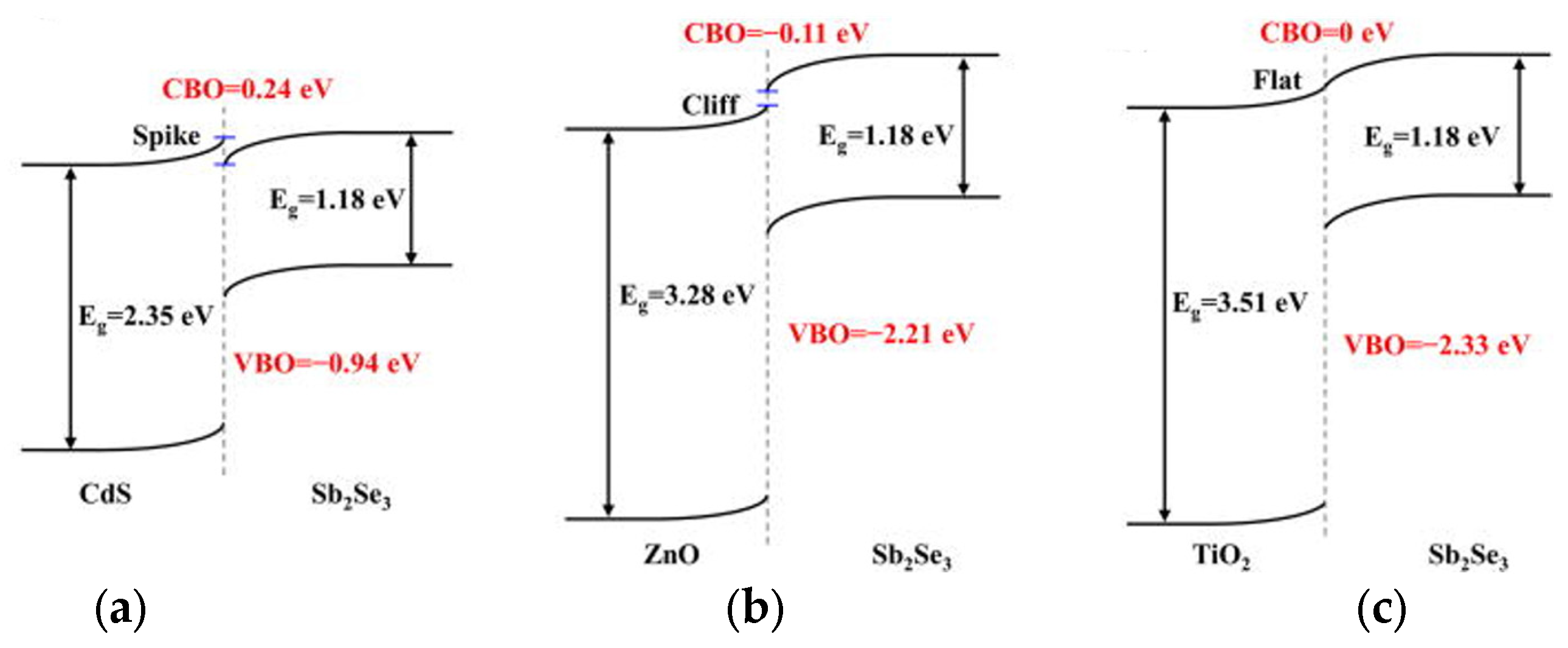
- Shiel, H.; Hutter, O.S.; Phillips, L.J.; Swallow, J.E.N.; Jones, L.A.H.; Featherstone, T.J.; Smiles, M.J.; Thakur, P.K.; Lee, T.-L.; Dhanak, V.R.; et al. Natural Band Alignments and Band Offsets of Sb2Se3 Solar Cells. ACS Appl. Energy Mater. 2020, 3, 11617–11626. [Google Scholar] [CrossRef]
- Lu, S.; Ding, H.; Hu, J.; Liu, Y.; Zhu, J.; Kondrotas, R.; Chen, C.; Tang, J. In Situ Investigation of Interfacial Properties of Sb2Se3 Heterojunctions. Appl. Phys. Lett. 2020, 116, 241602. [Google Scholar] [CrossRef]
- Mavlonov, A.; Razykov, T.; Raziq, F.; Gan, J.; Chantana, J.; Kawano, Y.; Nishimura, T.; Wei, H.; Zakutayev, A.; Minemoto, T.; et al. A Review of Sb2Se3 Photovoltaic Absorber Materials and Thin-Film Solar Cells. Sol. Energy 2020, 201, 227–246. [Google Scholar] [CrossRef]
- Rahman, F.; Alam Moon, M.; Hossain, M.K.; Ali, H.; Haque, D.; Kuddus, A.; Hossain, J.; Ismail, A.B. Concurrent Investigation of Antimony Chalcogenide (Sb2Se3 and Sb2S3)-Based Solar Cells with a Potential WS2 Electron Transport Layer. Heliyon 2022, 8, e12034. [Google Scholar] [CrossRef] [PubMed]
- Ayala-Mató, F.; Vigil-Galán, O.; Seuret-Jiménez, D.; Courel, M.; Fernández, S. Evaluation of Cd1–xZnxS as Electron Transport Layer in Superstrate and Inverted Configurations of Sb2Se3 Solar Cells with n-i-p Structure. Semicond. Sci. Technol. 2021, 36, 015016. [Google Scholar] [CrossRef]
- Salem, M.S.; Shaker, A.; Abouelatta, M.; Alanazi, A.; Al-Dhlan, K.A.; Almurayziq, T.S. Numerical Analysis of Hole Transport Layer-Free Antimony Selenide Solar Cells: Possible Routes for Efficiency Promotion. Opt. Mater. 2022, 129, 112473. [Google Scholar] [CrossRef]
- Kumari, R.; Mamta, M.; Kumar, R.; Singh, Y.; Singh, V.N. 24% Efficient, Simple ZnSe/Sb2Se3 Heterojunction Solar Cell: An Analysis of PV Characteristics and Defects. ACS Omega 2023, 8, 1632–1642. [Google Scholar] [CrossRef]
- Luo, Y.; Chen, G.; Chen, S.; Ahmad, N.; Azam, M.; Zheng, Z.; Su, Z.; Cathelinaud, M.; Ma, H.; Chen, Z.; et al. Carrier Transport Enhancement Mechanism in Highly Efficient Antimony Selenide Thin-Film Solar Cell. Adv. Funct. Mater. 2023, 33, 2213941. [Google Scholar] [CrossRef]
- Cai, H.; Cao, R.; Gao, J.; Qian, C.; Che, B.; Tang, R.; Zhu, C.; Chen, T. Interfacial Engineering towards Enhanced Photovoltaic Performance of Sb2Se3 Solar Cell. Adv. Funct. Mater. 2022, 32, 2208243. [Google Scholar] [CrossRef]
- Cheng, J.; Zhang, Z.; Zhao, M.; Guan, Y.; Chen, X.; Meng, X.; Tang, H.; Li, L.; Wang, S. High-Efficiency Sb2Se3 Thin-Film Solar Cells Based on Cd(S,O) Buffer Layers Prepared via Spin-Coating. Mater. Chem. Phys. 2023, 303, 127794. [Google Scholar] [CrossRef]
- Liu, Y.; Li, B.; Liang, X.; Liu, T.; Wang, S.; Li, Z. Reactively Sputtered CdS:O Buffer Layers for Substrate Sb2Se3 Solar Cells. J. Alloys Compd. 2023, 932, 167313. [Google Scholar] [CrossRef]
- Guo, L.; Zhang, B.; Ranjit, S.; Wall, J.; Saurav, S.; Hauser, A.J.; Xing, G.; Li, L.; Qian, X.; Yan, F. Interface Engineering via Sputtered Oxygenated CdS:O Window Layer for Highly Efficient Sb2Se3 Thin-Film Solar Cells with Efficiency Above 7%. Sol. RRL 2019, 3, 1900225. [Google Scholar] [CrossRef]
- Mao, X.; Wang, C.; Bian, M.; Wan, L.; Yang, X.; Zhou, R. The Design of SnO2-Dominated Electron Transport Layer for High-Efficiency Sb2(S,Se)3 Solar Cells. Phys. Status Solidi A 2022, 219, 2200576. [Google Scholar] [CrossRef]
- Li, G.; Li, Z.; Liang, X.; Guo, C.; Shen, K.; Mai, Y. Improvement in Sb2Se3 Solar Cell Efficiency through Band Alignment Engineering at the Buffer/Absorber Interface. ACS Appl. Mater. Interfaces 2019, 11, 828–834. [Google Scholar] [CrossRef]
- Zhou, J.; Zhang, X.; Chen, H.; Tang, Z.; Meng, D.; Chi, K.; Cai, Y.; Song, G.; Cao, Y.; Hu, Z. Dual-Function of CdCl2 Treated SnO2 in Sb2Se3 Solar Cells. Appl. Surf. Sci. 2020, 534, 147632. [Google Scholar] [CrossRef]
- Wen, S.; Yin, X.; Zhang, C.; Guo, Y.; Liu, J.; Wang, E.; Zheng, C.; Que, W.; Liu, H.; Liu, W. Achievable Efficiency Improvement of Sb2Se3 Thin-Film Solar Cells through Interface Engineering. Mater. Lett. 2021, 283, 128770. [Google Scholar] [CrossRef]
- Chen, Z.; Guo, H.; Ma, C.; Wang, X.; Jia, X.; Yuan, N.; Ding, J. Efficiency Improvement of Sb2Se3 Solar Cells Based on La-Doped SnO2 Buffer Layer. Sol. Energy 2019, 187, 404–410. [Google Scholar] [CrossRef]
- Wang, Y.; Tang, R.; Huang, L.; Qian, C.; Lian, W.; Zhu, C.; Chen, T. Post-Treatment of TiO2 Film Enables High-Quality Sb2Se3 Film Deposition for Solar Cell Applications. ACS Appl. Mater. Interfaces 2022, 14, 33181–33190. [Google Scholar] [CrossRef]
- Wang, X.; Guo, H.; Chen, Z.; Ma, C.; Fang, X.; Jia, X.; Yuan, N.; Ding, J. Enhancement of Sb2Se3 Thin-Film Solar Cell Photoelectric Properties by Addition of Interlayer CeO2. Sol. Energy 2019, 188, 218–223. [Google Scholar] [CrossRef]
- Zhang, J.; Guo, H.; Jia, X.; Ning, H.; Ma, C.; Wang, X.; Qiu, J.; Yuan, N.; Ding, J. Improving the Performance of Sb2Se3 Thin-Film Solar Cells Using n-Type MoO3 as the Back Contact Layer. Sol. Energy 2021, 214, 231–238. [Google Scholar] [CrossRef]
- Wang, W.; Yao, L.; Dong, J.; Wu, L.; Cao, Z.; Hui, L.; Chen, G.; Luo, J.; Zhang, Y. Interface Modification Uncovers the Potential Application of SnO2/TiO2 Double Electron Transport Layer in Efficient Cadmium-Free Sb2Se3 Devices. Adv. Mater. Interfaces 2022, 9, 2102464. [Google Scholar] [CrossRef]
- Luo, Y.-D.; Chen, M.; Tang, R.; Azam, M.; Chen, S.; Zheng, Z.-H.; Su, Z.-H.; Fan, P.; Ma, H.-L.; Liang, G.-X.; et al. Energy Band Alignment for Cd-Free Antimony Triselenide Substrate Structured Solar Cells by Co-Sputtering ZnSnO Buffer Layer. Sol. Energy Mater. Sol. Cells 2022, 240, 111721. [Google Scholar] [CrossRef]
- Dong, Y.; Huang, L.; Wang, H.; Peng, X.; Wang, Y.; Tang, R.; Zhu, C.; Chen, T. Zinc Chloride-Treated Indium Sulfide as Buffer Layer for Cd-Free Antimony Selenide Solar Cells. Sol. RRL 2023, 7, 2300440. [Google Scholar] [CrossRef]
- Cheng, C.-H.; Li, M.; Song, H.-Q.; Li, W.-H.; Leng, J.; Tian, W.; Cui, R.; Zhao, C.; Jin, S.; Liu, W.; et al. Enhanced Performance of the Sb2Se3 Thin-Film Solar Cell by Organic Molecule-Induced Crystallization and Suppression of the Interface Recombination. ACS Appl. Energy Mater. 2021, 4, 5079–5085. [Google Scholar] [CrossRef]
- Rovira, D.; Ros, E.; Tom, T.; Jiménez, M.; Miguel Asensi, J.; Voz, C.; López-Vidrier, J.; Puigdollers, J.; Bertomeu, J.; Saucedo, E. Polymeric Interlayer in CdS-Free ElectronSelective Contact for Sb2Se3 Thin-Film Solar Cells. Int. J. Mol. Sci. 2023, 24, 3088. [Google Scholar] [CrossRef] [PubMed]
- Li, K.; Wang, S.; Chen, C.; Kondrotas, R.; Hu, M.; Lu, S.; Wang, C.; Chen, W.; Tang, J. 7.5% n–i–p Sb2Se3 Solar Cells with CuSCN as a Hole-Transport Layer. J. Mater. Chem. A 2019, 7, 9665–9672. [Google Scholar] [CrossRef]
- Liu, C.; Shen, K.; Lin, D.; Cao, Y.; Qiu, S.; Zheng, J.; Bao, F.; Gao, Y.; Zhu, H.; Li, Z.; et al. Back Contact Interfacial Modification in Highly-Efficient All-Inorganic Planar n-i-p Sb2Se3 Solar Cells. ACS Appl. Mater. Interfaces 2020, 12, 38397–38405. [Google Scholar] [CrossRef]
- Zhang, J.; Kondrotas, R.; Lu, S.; Wang, C.; Chen, C.; Tang, J. Alternative Back Contacts for Sb2Se3 Solar Cells. Sol. Energy 2019, 182, 96–101. [Google Scholar] [CrossRef]
- Ma, Y.; Yin, Y.; Li, G.; Lian, W.; Zhang, J.; Tang, R.; Ju, H.; Chen, T. Aqueous Solution Processed MoS3 as an Eco-Friendly Hole-Transport Layer for All-Inorganic Sb2Se3 Solar Cells. Chem. Commun. 2020, 56, 15173–15176. [Google Scholar] [CrossRef]
- Lin, J.; Chen, G.; Ahmad, N.; Ishaq, M.; Chen, S.; Su, Z.; Fan, P.; Zhang, X.; Zhang, Y.; Liang, G. Back Contact Interfacial Modification Mechanism in Highly-Efficient Antimony Selenide Thin-Film Solar Cells. J. Energy Chem. 2023, 80, 256–264. [Google Scholar] [CrossRef]
- Cang, Q.; Guo, H.; Jia, X.; Ning, H.; Ma, C.; Zhang, J.; Yuan, N.; Ding, J. Enhancement in the Efficiency of Sb2Se3 Solar Cells by Adding Low Lattice Mismatch CuSbSe2 Hole Transport Layer. Sol. Energy 2020, 199, 19–25. [Google Scholar] [CrossRef]
- Liang, X.; Feng, Y.; Dang, W.; Huang, H.; Wang, X.; Guo, Y.; Shen, K.; Schropp, R.E.I.; Li, Z.; Mai, Y. High-Efficiency Flexible Sb2Se3 Solar Cells by Back Interface and Absorber Bulk Deep-Level Trap Engineering. ACS Energy Lett. 2023, 8, 213–221. [Google Scholar] [CrossRef]
- Hutter, O.S.; Phillips, L.J.; Durose, K.; Major, J.D. 6.6% Efficient Antimony Selenide Solar Cells Using Grain Structure Control and an Organic Contact Layer. Sol. Energy Mater. Sol. Cells 2018, 188, 177–181. [Google Scholar] [CrossRef]
- Don, C.H.; Shalvey, T.P.; Smiles, M.J.; Thomas, L.; Phillips, L.J.; Hobson, T.D.C.; Finch, H.; Jones, L.A.H.; Swallow, J.E.N.; Fleck, N.; et al. Multi-Phase Sputtered TiO2-Induced Current–Voltage Distortion in Sb2Se3 Solar Cells. Adv. Mater. Interfaces 2023, 10, 2300238. [Google Scholar] [CrossRef]
- Cao, Z.; Wang, W.; Dong, J.; Lou, L.; Liu, H.; Wang, Z.; Luo, J.; Liu, Y.; Dai, Y.; Li, D.; et al. Oxygen Content Modulation toward Highly Efficient Sb2Se3 Solar Cells. ACS Appl. Mater. Interfaces 2022, 14, 55691–55699. [Google Scholar] [CrossRef]
- Cao, Y.; Zhu, X.; Chen, H.; Zhang, X.; Zhouc, J.; Hu, Z.; Pang, J. Towards High Efficiency Inverted Sb2Se3 Thin Film Solar Cells. Sol. Energy Mater. Sol. Cells 2019, 200, 109945. [Google Scholar] [CrossRef]
- Sunny, A.; Ahmed, S.R.A. Numerical Simulation and Performance Evaluation of Highly Efficient Sb2Se3 Solar Cell with Tin Sulfide as Hole Transport Layer. Phys. Status Solidi B 2021, 258, 2000630. [Google Scholar] [CrossRef]
- Campbell, S.; Phillips, L.J.; Major, J.D.; Hutter, O.S.; Voyce, R.; Qu, Y.; Beattie, N.S.; Zoppi, G.; Barrioz, V. Routes to Increase Performance for Antimony Selenide Solar Cells Using Inorganic Hole Transport Layers. Front. Chem. 2022, 10, 954588. [Google Scholar] [CrossRef]
- Pasini, S.; Spoltore, D.; Parisini, A.; Marchionna, S.; Fornasini, L.; Bersani, D.; Fornari, R.; Bosio, A. Innovative Back-Contact for Sb2Se3-Based Thin Film Solar Cells. Sol. Energy 2023, 249, 414–423. [Google Scholar] [CrossRef]
- Li, Y.; Zhou, Y.; Luo, J.; Chen, W.; Yang, B.; Wen, X.; Lu, S.; Chen, C.; Zeng, K.; Song, H.; et al. The Effect of Sodium on Antimony Selenide Thin Film Solar Cells. RSC Adv. 2016, 6, 87288–87293. [Google Scholar] [CrossRef]
- Li, W.-H.; Li, M.; Hu, Y.-J.; Cheng, C.-H.; Kan, Z.-M.; Yu, D.; Leng, J.; Jin, S.; Cong, S. Enhanced Performance of Antimony Selenide Thin Film Solar Cell Using PbI2 as a Dopant. Appl. Phys. Lett. 2021, 118, 093903. [Google Scholar] [CrossRef]
- Huang, M.; Lu, S.; Li, K.; Lu, Y.; Chen, C.; Tang, J.; Chen, S. P-Type Antimony Selenide via Lead Doping. Sol. RRL 2022, 6, 2100730. [Google Scholar] [CrossRef]
- Ma, Y.; Tang, B.; Lian, W.; Wu, C.; Wang, X.; Ju, H.; Zhu, C.; Fan, F.; Chen, T. Efficient Defect Passivation of Sb2Se3 Film by Tellurium Doping for High Performance Solar Cells. J. Mater. Chem. A 2020, 8, 6510–6516. [Google Scholar] [CrossRef]
- Tiwari, K.J.; Neuschitzer, M.; Espindola, M.; Sanchez, Y.; Vidal, P.; Saucedo, E.; Malar, P. Tailoring Doping of Efficient Sb2Se3 Solar Cells in Substrate Configuration by Low Temperature Post Deposition Selenization Process. In Proceedings of the 2018 IEEE 7th World Conference on Photovoltaic Energy Conversion (WCPEC) (A Joint Conference of 45th IEEE PVSC, 28th PVSEC & 34th EU PVSEC), Waikoloa Village, HI, USA, 10–15 June 2018; IEEE: Waikoloa Village, HI, USA, 2018; pp. 1858–1860. [Google Scholar] [CrossRef]
- Spaggiari, G.; Bersani, D.; Calestani, D.; Gilioli, E.; Gombia, E.; Mezzadri, F.; Casappa, M.; Pattini, F.; Trevisi, G.; Rampino, S. Exploring Cu-Doping for Performance Improvement in Sb2Se3 Photovoltaic Solar Cells. Int. J. Mol. Sci. 2022, 23, 15529. [Google Scholar] [CrossRef] [PubMed]
- Li, Y.; Zhou, Y.; Zhu, Y.; Chen, C.; Luo, J.; Ma, J.; Yang, B.; Wang, X.; Xia, Z.; Tang, J. Characterization of Mg and Fe Doped Sb2Se3 Thin Films for Photovoltaic Application. Appl. Phys. Lett. 2016, 109, 232104. [Google Scholar] [CrossRef]
- Liu, X.; Xiao, X.; Yang, Y.; Xue, D.-J.; Li, D.-B.; Chen, C.; Lu, S.; Gao, L.; He, Y.; Beard, M.C.; et al. Enhanced Sb2Se3 Solar Cell Performance through Theory-Guided Defect Control: Enhanced Sb2Se3 Solar Cell Performance. Prog. Photovolt. Res. Appl. 2017, 25, 861–870. [Google Scholar] [CrossRef]
- Hobson, T.D.C.; Phillips, L.J.; Hutter, O.S.; Shiel, H.; Swallow, J.E.N.; Savory, C.N.; Nayak, P.K.; Mariotti, S.; Das, B.; Bowen, L.; et al. Isotype Heterojunction Solar Cells Using N-Type Sb2Se3 Thin Films. Chem. Mater. 2020, 32, 2621–2630. [Google Scholar] [CrossRef]
- Hobson, T.D.C.; Shiel, H.; Savory, C.N.; Swallow, J.E.N.; Jones, L.A.H.; Featherstone, T.J.; Smiles, M.J.; Thakur, P.K.; Lee, T.-L.; Das, B.; et al. P-Type Conductivity in Sn-Doped Sb2Se3. J. Phys. Energy 2022, 4, 045006. [Google Scholar] [CrossRef]
- Chen, S.; Qiao, X.; Zheng, Z.; Cathelinaud, M.; Ma, H.; Fan, X.; Zhang, X. Enhanced Electrical Conductivity and Photoconductive Properties of Sn-Doped Sb2Se3 Crystals. J. Mater. Chem. C 2018, 6, 6465–6470. [Google Scholar] [CrossRef]
- Costa, M.B.; De Souza Lucas, F.W.; Mascaro, L.H. Electrodeposition of Fe-Doped Sb2Se3 Thin Films for Photoelectrochemical Applications and Study of the Doping Effects on Their Properties. J. Solid State Electrochem. 2018, 22, 1557–1562. [Google Scholar] [CrossRef]
- Zhou, H.; Feng, M.; Feng, M.; Gong, X.; Zhang, D.; Zhou, Y.; Chen, S. Gradient Doping of Sulfur in Sb2Se3 Nanowire Arrays as Photoelectrochemical Photocathode with a 2% Half-Cell Solar-to-Hydrogen Conversion Efficiency. Appl. Phys. Lett. 2020, 116, 113902. [Google Scholar] [CrossRef]
- Baghbanzadeh-Dezfuli, B.; Jamali-Sheini, F.; Cheraghizade, M. Electrochemical Synthesis of S-Doped Sb2Se3 Nanostructures and Photo-Switching Behaviour. Opt. Quantum Electron. 2023, 55, 4. [Google Scholar] [CrossRef]
- Gautam, S.; Thakur, A.; Tripathi, S.K.; Goyal, N. Effect of Silver Doping on the Electrical Properties of A- Sb2Se3. J. Non-Cryst. Solids 2007, 353, 1315–1321. [Google Scholar] [CrossRef]
- Wu, W.; Li, Y.; Liang, L.; Hao, Q.; Zhang, J.; Liu, H.; Liu, C. Enhanced Broadband Responsivity of Ni-Doped Sb2Se3 Nanorod Photodetector. J. Phys. Chem. C 2019, 123, 14781–14789. [Google Scholar] [CrossRef]
- Li, J.; Wang, B.; Liu, F.; Yang, J.; Li, J.; Liu, J.; Jia, M.; Lai, Y.; Liu, Y. Preparation and Characterization of Bi-Doped Antimony Selenide Thin Films by Electrodeposition. Electrochim. Acta 2011, 56, 8597–8602. [Google Scholar] [CrossRef]
- Chen, S.; Luo, P.; Ren, D.-L.; Duan, C.-Y.; Ma, X.-F.; Su, Z.-H.; Zheng, Z.-H.; Fan, P.; Liang, G.-X.; Tang, R. An Effective Engineering with Simultaneous Carrier Density Enhancement and Interface Optimization Enables Efficient Sb2Se3 Solar Cells. Appl. Surf. Sci. 2023, 619, 156783. [Google Scholar] [CrossRef]
- Chen, G.; Li, X.; Abbas, M.; Fu, C.; Su, Z.; Tang, R.; Chen, S.; Fan, P.; Liang, G. Tellurium Doping Inducing Defect Passivation for Highly Effective Antimony Selenide Thin Film Solar Cell. Nanomaterials 2023, 13, 1240. [Google Scholar] [CrossRef] [PubMed]


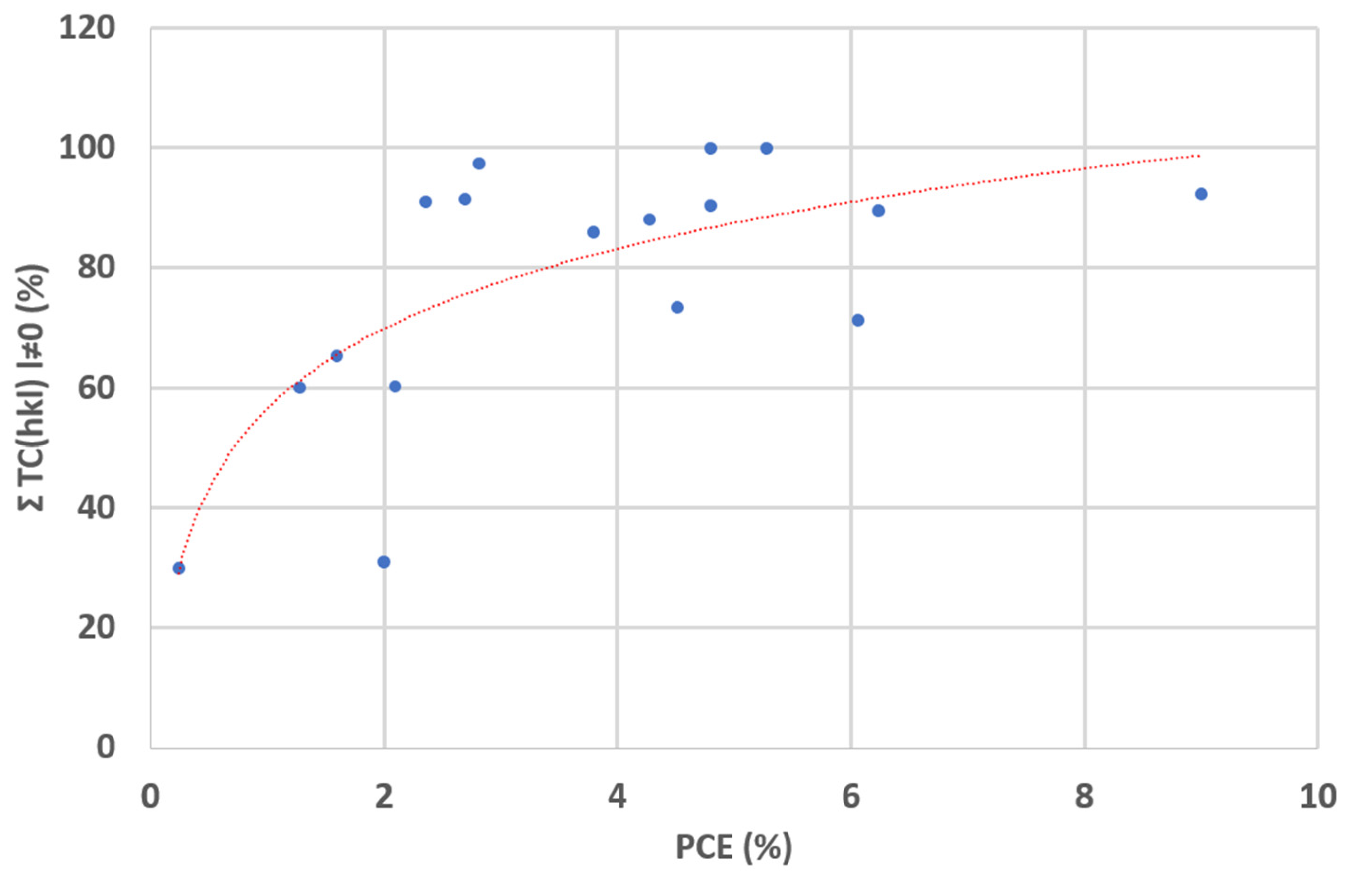
| Deposition Method | Substrate/ Underlayer | Σ TC (hkℓ) ℓ ≠ 0 | Observations | PCE | Jsc (mA/cm2) | Reference |
|---|---|---|---|---|---|---|
| CSS | TiO2/FTO/glass | 86% | With seeding layer | 3.8% | 21.1 | [36] |
| CSS | TiO2/FTO/glass | 65.4% | W/o seeding layer | 1.6% | 24.9 | [36] |
| CSS | CdS/FTO/glass | 89.5% | CdCl2 treatment | 6.23% | 27.36 | [36] |
| CSS | CdS/FTO/glass | 88.1% | // | 4.27% | 21.74 | [21] |
| CSS | CdS/FTO/glass | 97.5% | CdS by CCS | 2.82% | 19.5 | [37] |
| CSS | TiO2/FTO/glass | ~100% | Seeding layer | 5.28% | 24.6 | [37] |
| CSS | TiO2/CdS/FTO/glass | ~100% | // | 2.07% | 15.6 | [37] |
| CSS | SnO2/FTO/glass | 58.3% | CdCl2 treatment | // | // | [38] |
| CSS | SnO2/FTO/glass | 5.4% | No treatments | // | // | [38] |
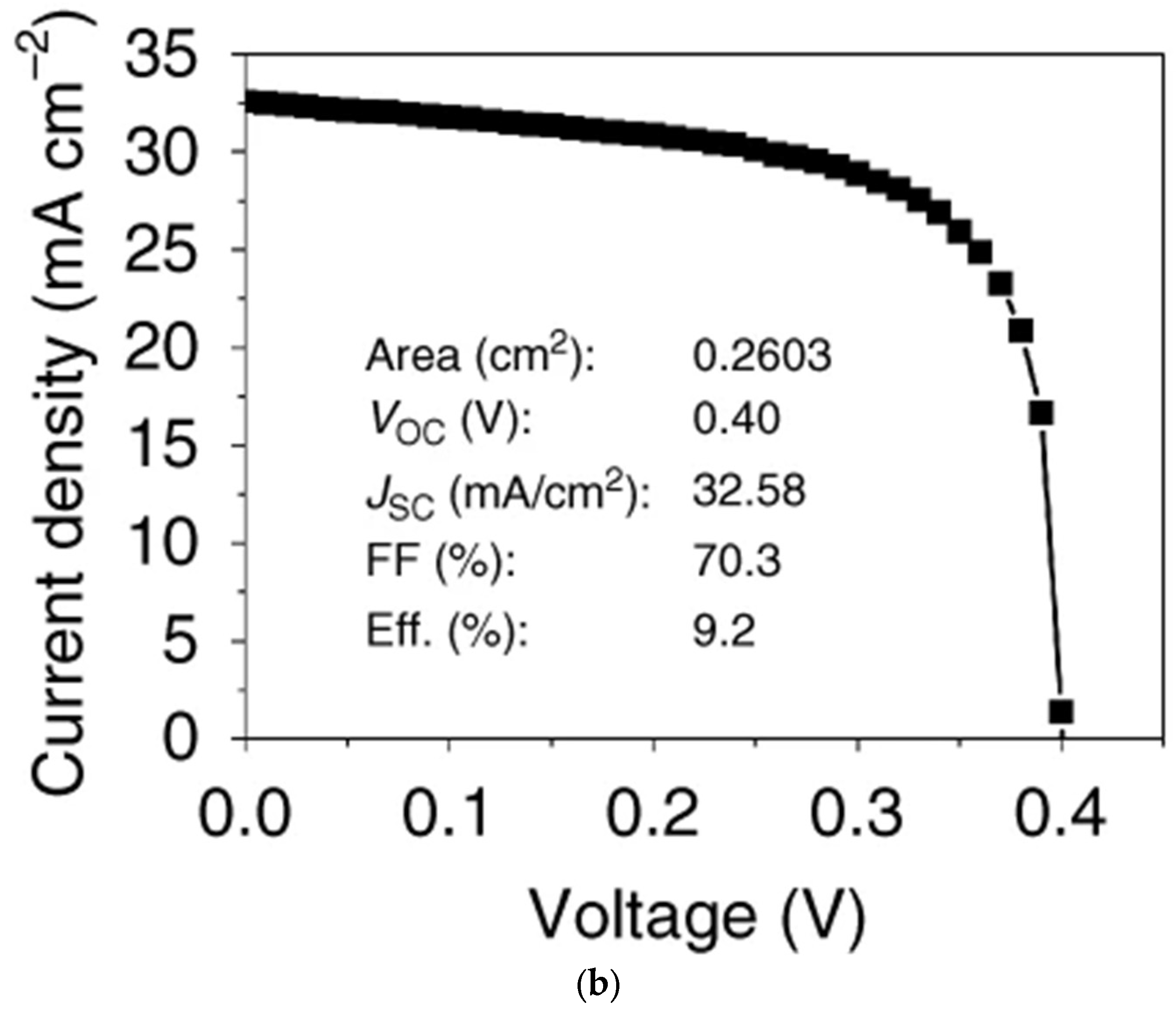
| CSS | FTO/glass | 92.2% | 330 °C | 9% | 29.8 | [39] |
| VTD | SnO2/ITO/glass | 91.4% | // | 2.7% | 19.3 | [40] |
| VTD | TiO2/ITO/glass | 30.9% | // | 2% | 23.6 | [40] |
| VTD | SnO2/TiO2/ITO/glass | ~100% | // | 4.8% | 25.6 | [40] |
| VTD | CdS/TiO2/ITO/glass | 64.7% | CdS-VTD | 4.91% | 28.6 | [41] |
| VTD | CdS/TiO2/ITO/glass | 50.1% | CdS-CBD | 4.24% | 28.3 | [41] |
| RTE | CdS/FTO/glass | 90.4% | w/o KOH treatment | 4.8% | 28.13 | [26] |
| RTE | CdS/FTO/glass | 92.1% | with KOH treatment | 7.16% | // | [26] |
| RF sputtering | CdS/FTO/glass | 71.3% | Annealing at 460 °C | 6.06% | 25.91 | [42] |
| RF sputtering | FTO/glass | 60% | // | 1.28% | 24.83 | [19] |
| RF sputtering | CdS/FTO/glass | 91% | // | 2.36% | 27.06 | [19] |
| RF sputtering | Mo | 30% | // | 0.24% | 5.11 | [19] |
| PED | FTO/glass | 60.2% | // | 2.1% | 20.3 | [32] |
| PED | CdS/FTO/glass | 38.4% | // | // | // | [32] |
| PED | Mo | 0.6% | // | // | 0.3 | [32] |
| Thermal co-evaporation | Mo | 73.5% | Substrate T = 300 °C | 2.67–4.51% | 19.51 | [43] |
| ETL | HTL | PCE | Absorber Deposition Method | Reference |
|---|---|---|---|---|
| CdS:Al | / | 8.41% | RF-MS + selenization | [67] |
| Sb-CdS | SpirOmetad | 6.13% | RTE | [68] |
| Cd(S,O) | / | 5.76% | Thermal evaporation | [69] |
| CdS:O | MoSe2 | 7.69% | CSS | [70] |
| CdS/SnO2 | SpirOmetad | 8% | Hydrothermal | [72] |
| CdZnS | / | 6.71% | CSS | [73] |
| CdS | / | 5.08% | CSS | [73] |
| SnO2 | P3HT | 4.76% | CSS | [74] |
| CdS/TiO2/SnO2 | / | 7% | VTD | [40] |
| CdS/TiO2 | / | 5.82% | VTD | [80] |
| SnO2 | / | 4.03% | VTD | [75] |
| La-SnO2 | / | 3.25% | RTE | [76] |
| TiO2 (CdCl2 treatment) | SpirOmetad | 6.06% | Thermal evaporation | [77] |
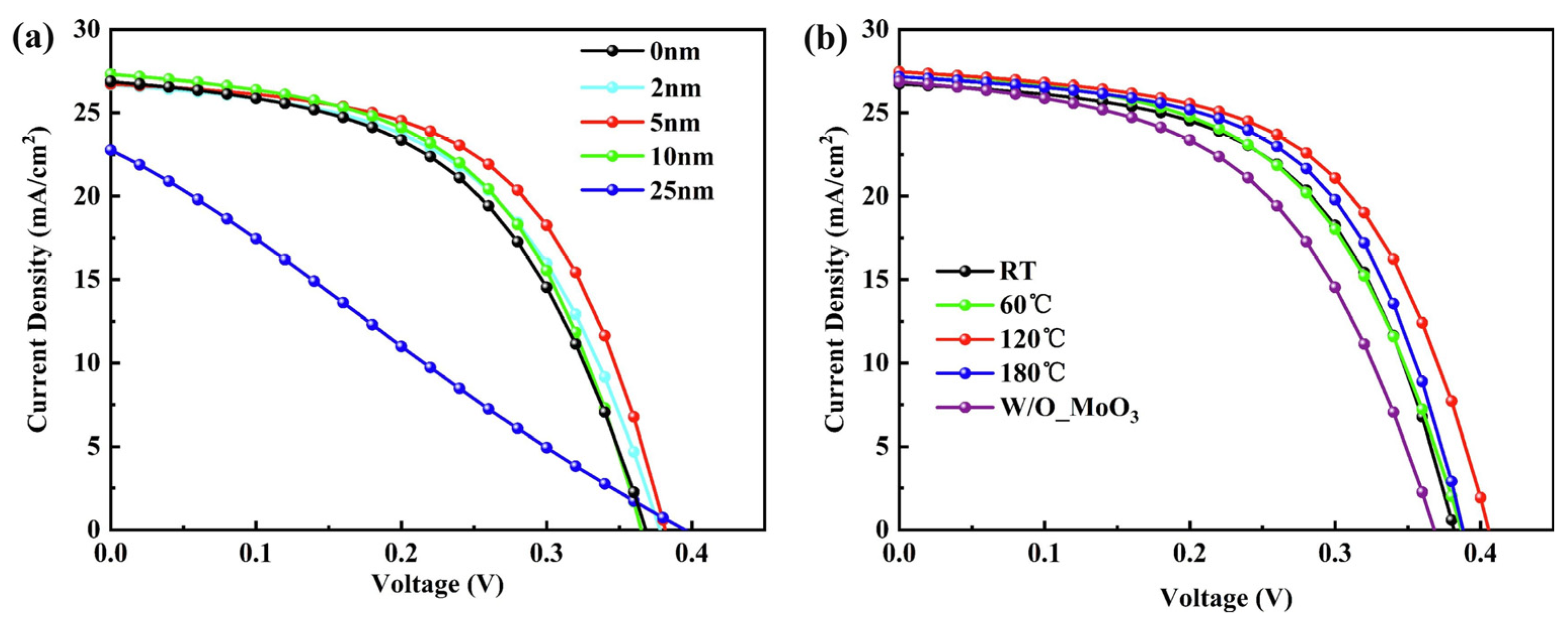
| MoO3 | CdS | 6.3% | RTE | [79] Figure 8 |
| ZTO | / | 3.44% | Magnetron cosputtering | [81] |
| InCl2–In2S3 | SpirOmetad | 5.0% | VTE | [82] |
| C60 | NPB | 5.03% | VTE | [83] |
| CdS | CuSCN | 7.5% | VTD | [85] |
| CdS | WO3−x/ | 7.1% | CSS | [86] |
| CdS/TiO2 | MoSe2 | 9.2% | CSS | [25] Figure 5b |
| CdS | MoSe2 | 10.12% | IVD | [29] Figure 2d |
| CdS:O | / | 7% | CSS | [71] |
| CeO2 | / | 5.14% | RTE | [78] |
| CdS | NiOx | 6.5% | VTD | [87] |
| SnO2/CdS | t-Se | 7.45% | CSS | [34] |
| CdS | MoS3 | 6.65% | TE | [88] |
| CdS | MoO2 | 8.14% | RF-MS + selenization | [89] |
| CdS | CuSbSe2 | 5.87% | VTD | [90] |
| CdS | Mo/PbSe | 8.4% | CSS | [91] |
| TiO2 | PCDTBT | 6.6% | CSS | [92] |
| TiO2 | P3HT | 6.88% | CSS | [93] |
| CdS | SpirOmetad | 7.27% | VTD | [94] |
Disclaimer/Publisher’s Note: The statements, opinions and data contained in all publications are solely those of the individual author(s) and contributor(s) and not of MDPI and/or the editor(s). MDPI and/or the editor(s) disclaim responsibility for any injury to people or property resulting from any ideas, methods, instructions or products referred to in the content. |
© 2023 by the authors. Licensee MDPI, Basel, Switzerland. This article is an open access article distributed under the terms and conditions of the Creative Commons Attribution (CC BY) license (https://creativecommons.org/licenses/by/4.0/).
Share and Cite
Jakomin, R.; Rampino, S.; Spaggiari, G.; Pattini, F. Advances on Sb2Se3 Solar Cells Fabricated by Physical Vapor Deposition Techniques. Solar 2023, 3, 566-595. https://doi.org/10.3390/solar3040031
Jakomin R, Rampino S, Spaggiari G, Pattini F. Advances on Sb2Se3 Solar Cells Fabricated by Physical Vapor Deposition Techniques. Solar. 2023; 3(4):566-595. https://doi.org/10.3390/solar3040031
Chicago/Turabian StyleJakomin, Roberto, Stefano Rampino, Giulia Spaggiari, and Francesco Pattini. 2023. "Advances on Sb2Se3 Solar Cells Fabricated by Physical Vapor Deposition Techniques" Solar 3, no. 4: 566-595. https://doi.org/10.3390/solar3040031