Article

Enhanced Electrical Properties of Alkali-Doped ZnO Thin Films with Chemical Process

Department of Inorganic and Organic Chemistry, University Jaume I, 12071 Castellon de la Plana, Spain
*
Author to whom correspondence should be addressed.
Solar 2021, 1(1), 30-40; https://doi.org/10.3390/solar1010004
Submission received: 22 October 2021 / Revised: 19 November 2021 / Accepted: 22 November 2021 / Published: 24 November 2021
(This article belongs to the Special Issue Solar Technologies—A Snapshot of the Editorial Board)

Abstract

:
Doped ZnO are among the most attractive transparent conductive oxides for solar cells because they are relatively cheap, can be textured for light trapping, and readily produced for large-scale coatings. Here, we focus on the development of alternative Na and K-doped ZnO prepared by an easy low-cost spray pyrolysis method for conducting oxide application. To enhance the electrical properties of zinc oxide, alkali-doped Zn1−x MxO (x = 0.03) solid solutions were investigated. The resulting layers crystallize in a single hexagonal phase of wurtzite structure with preferred c-axis orientation along a (002) crystal plane. Dense, well attached to the substrate, homogeneous and highly transparent layers were obtained with great optical transmittance higher than 80%. The optical energy band gap of doped ZnO films increase from 3.27 to 3.29 eV by doping with Na and K, respectively. The electrical resistivity of the undoped ZnO could be decreased from 1.03 × 10⁻¹ Ω.cm to 5.64 × 10⁻² Ω.cm (K-doped) and 3.18 × 10⁻² (Na-doped), respectively. Lastly, the carrier concentrations increased from 5.17 × 10¹⁷ (undoped ZnO) to 1 × 10¹⁸ (doped ZnO).

1. Introduction

Transparent conductive oxides (TCOs) are suitable materials for photovoltaic (PV) applications, light-emitting diodes, and others that can be functionalized depending on the requisites of its uses [1,2,3]. For many years, numerous other materials and devices have been proven with the ultimate goal to make photovoltaic energy widely available. Thin film technology is a suitable option for the replacement of the classical silicon crystalline solar cells [4]. The request of the TCOs layers needs high transparency as well as a low sheet resistivity. Most of the current commercial devices are designed with tin-doped indium oxide In2O3:Sn (ITO) and fluorine-doped tin oxide SnO2:F (FTO) due to their good optical and electrical features [5,6,7]. Mainly, ITO is the most widely used TCO, because of its two crucial properties, its excellent electrical conductivity and optical transmittance [8,9].
In contrast, TCO based on ZnO films are widely used because they are relatively cheap, can be modulated for light absorption and readily shaped for large-scale coatings [10,11]. The direct bandgap for ZnO is EG = 3.37 eV, so these may lead to many applications, for example, in photonics [12]. On the other hand, the high exciton binding energy that ZnO has, around 60 meV at room temperature, is an important material property regard. In addition, ZnO is resistant to oxygen and moisture and it has very good optical transparency, easy solution processing, and a flexible host crystal lattice able to accept a variety of dopant substitutions [13]. ZnO exhibits an unintentional n-type character; it possesses a high number of electron donors. Additional doping could increase the donor concentration [14]. It is well known that the process of thin films doping with elements of group 13 of the periodic table (Al, Ga, and In) improves its electrical properties [15,16]. Another material property for a high number of applications where the electronic charge has to be transmitted is the mobility of charge carriers (electrons and holes). The values of the electron and holes mobility are also highly important considering the potential of this material in applications such as TCO: thanks to this, ZnO exhibits high charge carrier mobilities as compared to other compounds used in photovoltaic devices [17]. Different technologies for the preparation of TCOs layers are used, predominantly physical techniques such as magnetron sputtering and chemical vapor deposition [18], instead of chemical routes (sol-gel or spray pyrolysis) [19]. In general, chemical methods are promising ways for TCOs production due to their efficient material use and high throughput. The uses of sodium (Na) such as a ZnO dopant to obtain p-type heterojunctions onto Si or (1-102) sapphire substrates was researched, and they conclude the importance of Na concentration for exhibit n- or p-conductivity [20,21]. Recently, several groups reported obtaining p-type of ZnO by potassium (K) [22,23]; although, the deposited ZnO:K onto glass substrate suffers the same problem or exhibits n- or p-conductivity depending on the K doping, and the results of resistivity will also improve [24].
In this context, the influences of alkali doping (Na and K) on the ZnO properties were investigated. In this paper, we report the electrical, optical, and photochemical properties of doped ZnO (Zn0.97M0.03O, where M = Na, K) thin films prepared by low-cost and facile spray pyrolysis deposition onto a soda-lime glass substrate.

2. Materials and Methods

2.1. Synthesis and Deposition

A solid solution of Na and K-doped ZnO (Zn1−x MxO, x = 0.03) was prepared by the spray pyrolysis method [25]. Undoped ZnO for comparison studies was synthesized using the same method. The raw materials applied for the desired compounds were: Zn(CH3COO)2·2H2O (PanReac Applichem, 99.5%,), Na(CH3COO) (Labkem, 99.9%), and KNO3 (Labkem, 99%). The precursor solution was performed by dissolving the alkaline salts into the mixture of ethanol (EtOH) (25 mL) and methanolamine (MEA-C2H7NO) (1.12 mL) in M+/Zn3+ (M = Na, K) molar ratio = 3%; under constant stirring on a hot plate at room temperature.
The resulting solutions were applied by handmade Dual Action Gravity Feed Airbrush with flow rate was 5.75 mL/min onto a soda-lime glass substrate, previously treated by a mixture of HCl:HNO3 (1:2) for surface texturing. Then, the samples were heated at 425 °C at atmospheric pressure on a hot plate to eliminate the organic compounds. To increase the crystallinity of the coating, thermal treatment at 350 °C (heating rate 20 °C/min in a reductive atmosphere was performed.

2.2. Characterization Techniques

The crystal structure of doped ZnO thin film was studied using Grazing incidence X-ray diffraction (GIXRD) measurements. X-ray diffractometer (D4 Endeavor, Burker-ASX) equipped with a Cu Kα radiation source was used. Data was collected by step-scanning from 10° to 80° with a step size of 0.05° 2θ and 3 s counting time per step. The measurements were performed at a grazing-incident angle, greater than the so-called critical angle for total external reflection, at which X-rays penetrate the sample. The critical angle (around 1°) was determined experimentally.
Scanning electron microscopy (SEM) model JEOL 7001F was employed to study the morphology of the films. The layer thickness was determined from cross-section micrographs. The surface chemical analysis was investigated by X-ray photoelectron spectroscopy (XPS) on a Sage 150 photoelectron spectrometer for the multi-technique surface analysis system. This system was equipped with a MAC 2 CAMECA RIBER double stage cylindrical mirror electron-energy analyzer. The photon source was a CAMECA SCX 700 dual anode X-ray. A non-monochromatized Al Kα X-ray source (hν = 1486.6 eV) was used as the excitation source in all cases. Electrical measurements were carried out by the four-probe method using Ossila T2001A3 with a target current of 0.001A and a voltage increment of 0.01 V per point to a maximum of 10 V to obtain the sheet resistance and resistivity data.
The optical properties and band gap energy of the TCOs were conducted by UV–vis–NIR spectroscopy in the wavelength range 200–1000 nm (step size 1 nm) using a Cary 500 Scan Varian spectrophotometer. The transmittance spectra were obtained applying BaSO4 integrating sphere as white reference material.
The photoelectrochemical measurements were realize in a three-electrode system. The Na, and K-doped ZnO onto a soda-lime glass substrate was used as a working electrode having a surface area of about 0.6 cm2, Pt wire was used as work electrode and Ag/AgCl was used as a reference electrode, respectively. The electrolyte used for the measure was 1M KCl solution. The measurements were carried out with Autolab potentiostat/galvanostat PGSTAT302. Electrochemical impedance spectroscopy (EIS) measurements were completed between 50 mHz and 1 MHz with 20 mV amplitude perturbation, with a step potential of 64 mV in the anodic direction. The EIS data were evaluated with ZView software (Scribner Associates).

3. Results and Discussion

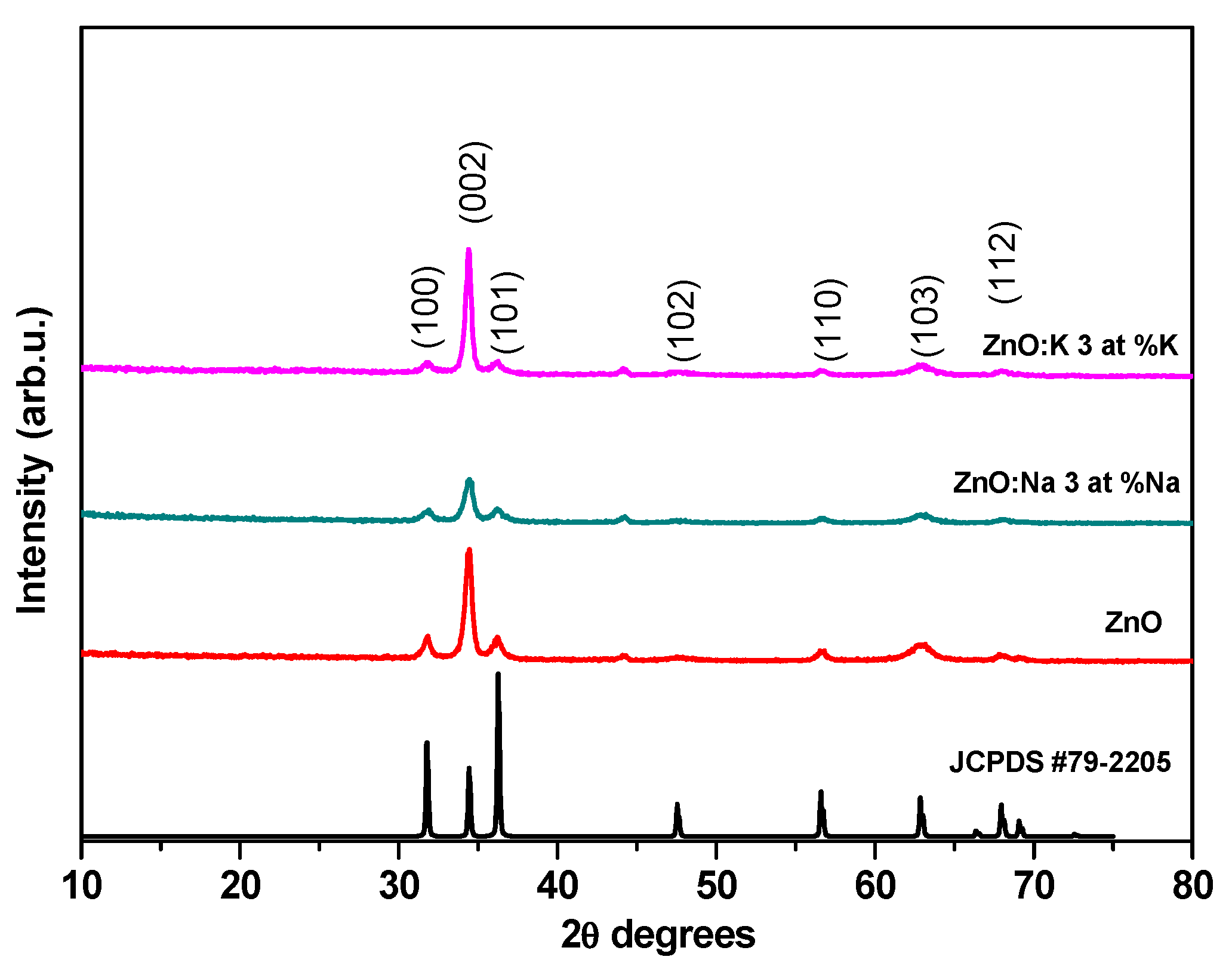
3.1. Crystallographic Properties of M-Doped ZnO (M = Na, K) Thin Films

In this study, structural changes in ZnO films deposited onto a soda-lime glass as a result of Na or K incorporation have been studied by Grazing incidence X-ray diffraction (GIXD). XRD patterns of undoped ZnO, ZnO:Na, and ZnO:K thin films were shown in Figure 1. All films show a strong peak at 2θ near 34, 42° and weak peaks at 31.80°, 36.21°, 56.60°, 62.85°, and 67.94° could be assigned, respectively, to the (002), (100), (101), (110), (103), and (112) crystal planes. This preferred c-axis orientation along the (002) plane is not new, it can be seen in other studies with different types of deposition techniques [26,27]. ZnO wurtzite structure could be occupied in principle by a Zn interstitial atom (Zni) in the tetrahedral site or the octahedral site. Zn interstitial will be more stable at the octahedral site where the geometrical constraints are less relentless. Moreover, the density-functional calculations indicate a large displacement of Zni along the c-axis instead of occupying the ideal octahedral site, resulting in an increased Zni–Zn distance [28,29]. Furthermore, all the observed diffraction peaks for TCO films which correspond to Bragg reflections of the wurtzite structure (JCPDS File No.79-2205). The absence of impurity peak shows that as-obtained films are highly phased pure. The different TCO thin films change the intensity, but the peak position does not change, depending on the type of doping within the sensitivity of the method.

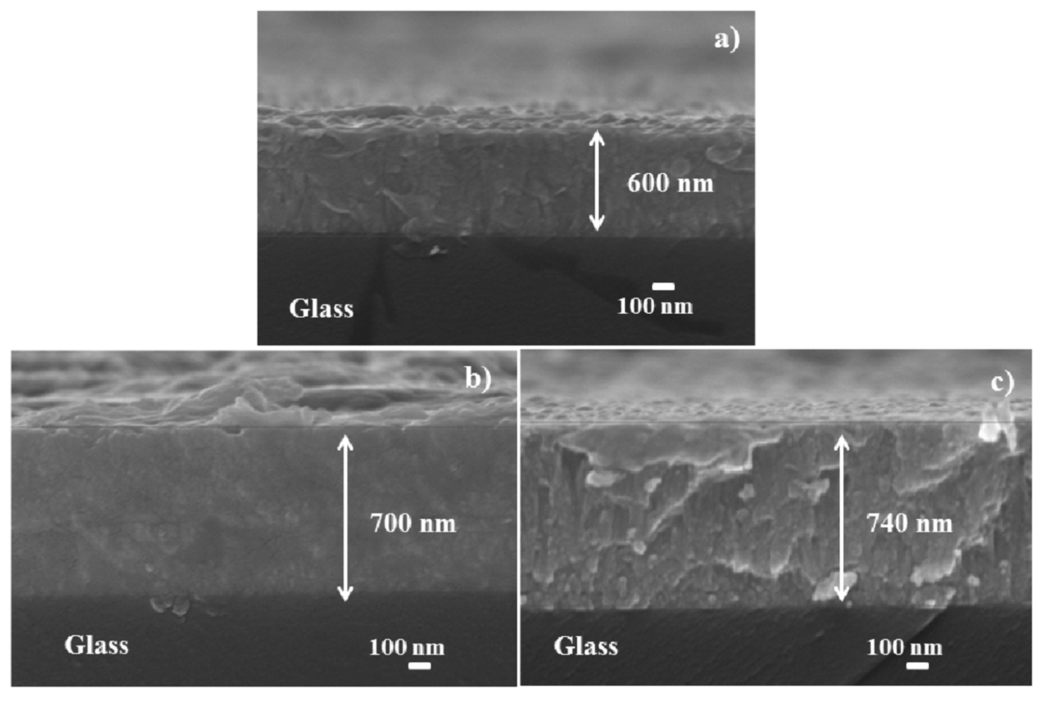
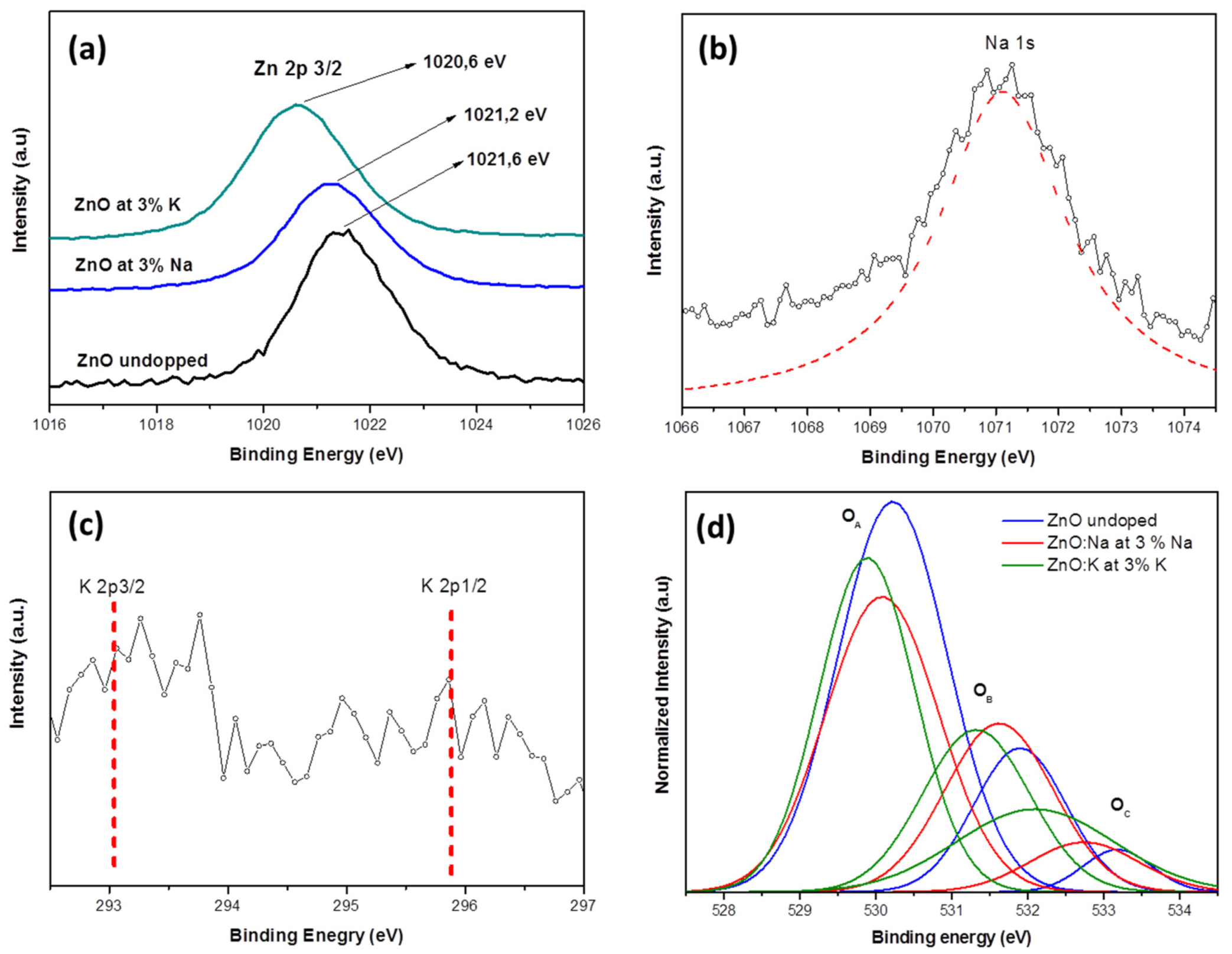
3.2. Morphological and Structural Properties of M-Doped ZnO (M = Na, K) Thin Films

Figure 2 shows the plan and cross-section images of the M-doped ZnO thin films. In all cases, dense and well attached homogeneous layers were observed in terms of particle size and distribution. Furthermore, a good separation could be seen between the film and the soda glass. The samples showed a thickness between 600 nm and 740 nm due to the manual method used.
To calculate the contained of the different dopant concentration in the films and to determinate the chemical state of the film composing elements, XPS analysis was carried out for undoped, 3% Na and 3% K-doped ZnO films, and calibrated according to the C 1s peak at ~285 eV. The XPS results confirm that Na and K elements have been doped into the ZnO film but the value of the atomic percentage of M-dopants in the thin film surface was variable. In the case of Na and K, the percentage the values of atomic percentage in the surface of the thin film (2.8% and 2.1%, respectively) are smaller than expected in the nominal composition in the solution (3% of dopant).
Figure 3a gives XPS data of the Zn 2p3/2 in the undoped ZnO films, Na and K-doped ZnO films. These peaks could be attributed to the position of Zn 2p in pure ZnO, and no metallic Zn with binding energy about 1021.6 eV is observed; it concludes that Zn can only found as the oxidized state. The Zn binding energy decreases while O binding energy increases when comparing undoped ZnO to Na or K-doped ZnO in the XPS data by other authors [30].
XPS spectrum and simulated lines of Na 1s in the ZnO:Na film is shown in Figure 3b. The peak position was at the binding energy of 1071.10 eV. This binding energy corresponds to Na+ oxide; it concludes that Na element doped as Na+ in the Na-doped ZnO film. Figure 3c reveals that K has been doped into ZnO crystal by the K 2p peaks that are observed in Figure 3b, similarly to previously report [31]. The binding states of O 1s coming from to the undoped ZnO, ZnO:Na, and ZnO:K are shown in Figure 3d. The asymmetric O 1s peak was coherently fitted by three Gaussian components, which are low binding energy peak (OA), medium binding energy peak (OB), and high binding energy peak (Oc) [32]. The OA peak of the 1s spectrum could be associated to the O2- ions on the wurtzite structure of the hexagonal Zn2+ ion array, which are encircled by zinc atoms with the full supplement of neighbor O2− ions [33]. Therefore, The OA peak of the 1s spectrum can be related to the Zn-O bonds [34]. The higher-binding energy (OC) is related to chemisorbed or dissociated oxygen or different species; for example, OH species on the surface of the ZnO films; for instance, CO3, adsorbed H2O, or absorbed O2 [35]. The OB of the O 1s peak is related to O2- ions that are in oxygen-deficient regions in the ZnO matrix [36,37]. The difference between the intensity of the peaks could attribute with the variation in the concentration of the oxygen vacancies (VO) [38]. The intensity of OA peaks in comparison with OB and OC explains the strong Zn-O bonding in ZnO thin films, the value of the binding energy for the different peaks (OA, OB, and OC) decrease when comparing undoped ZnO to Na or K-doped ZnO in other words when the atomic radio of the dopant increases the bonding energy of Zn-O decrease owning to the wurtzite structure was distorted.

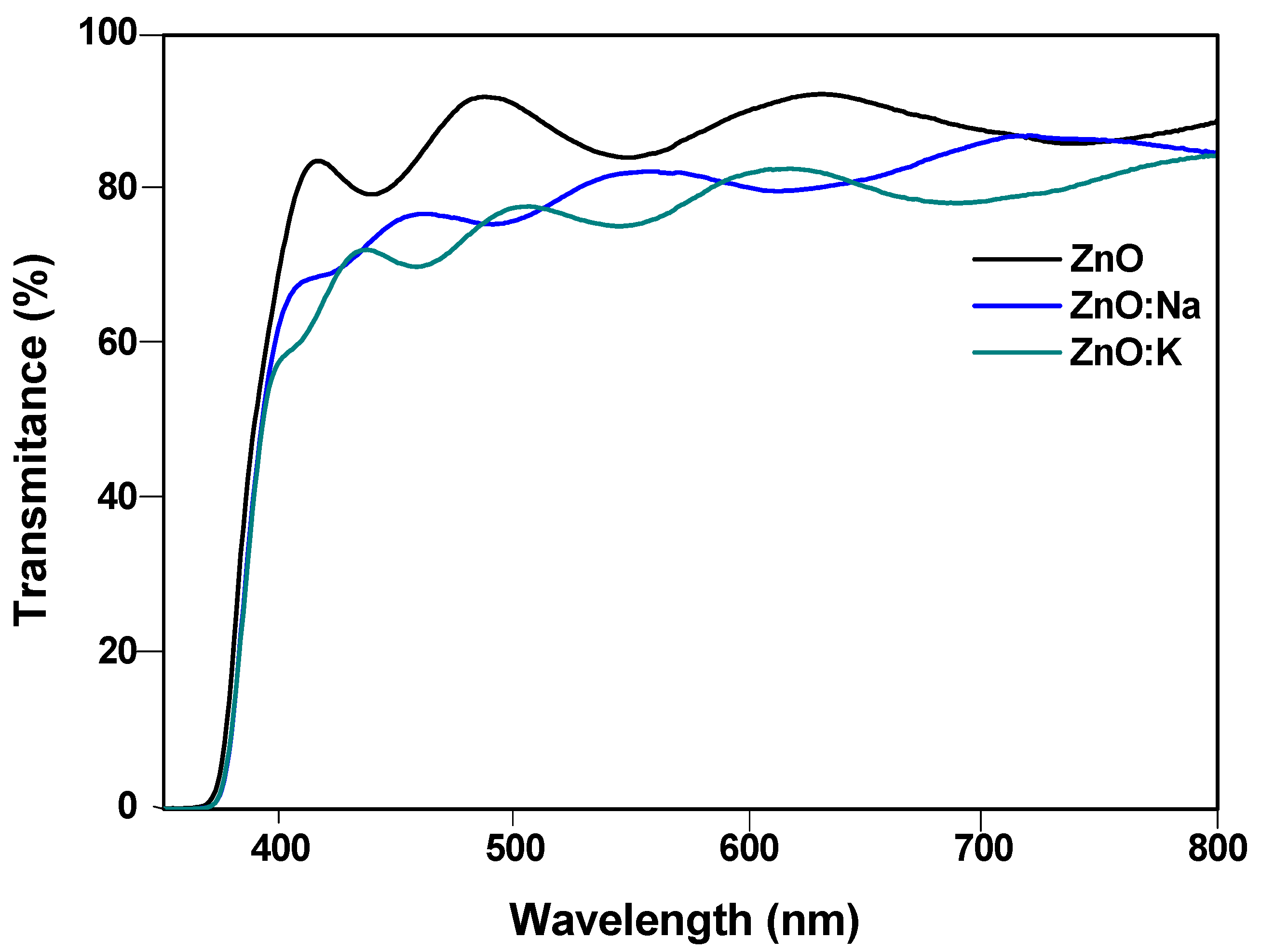
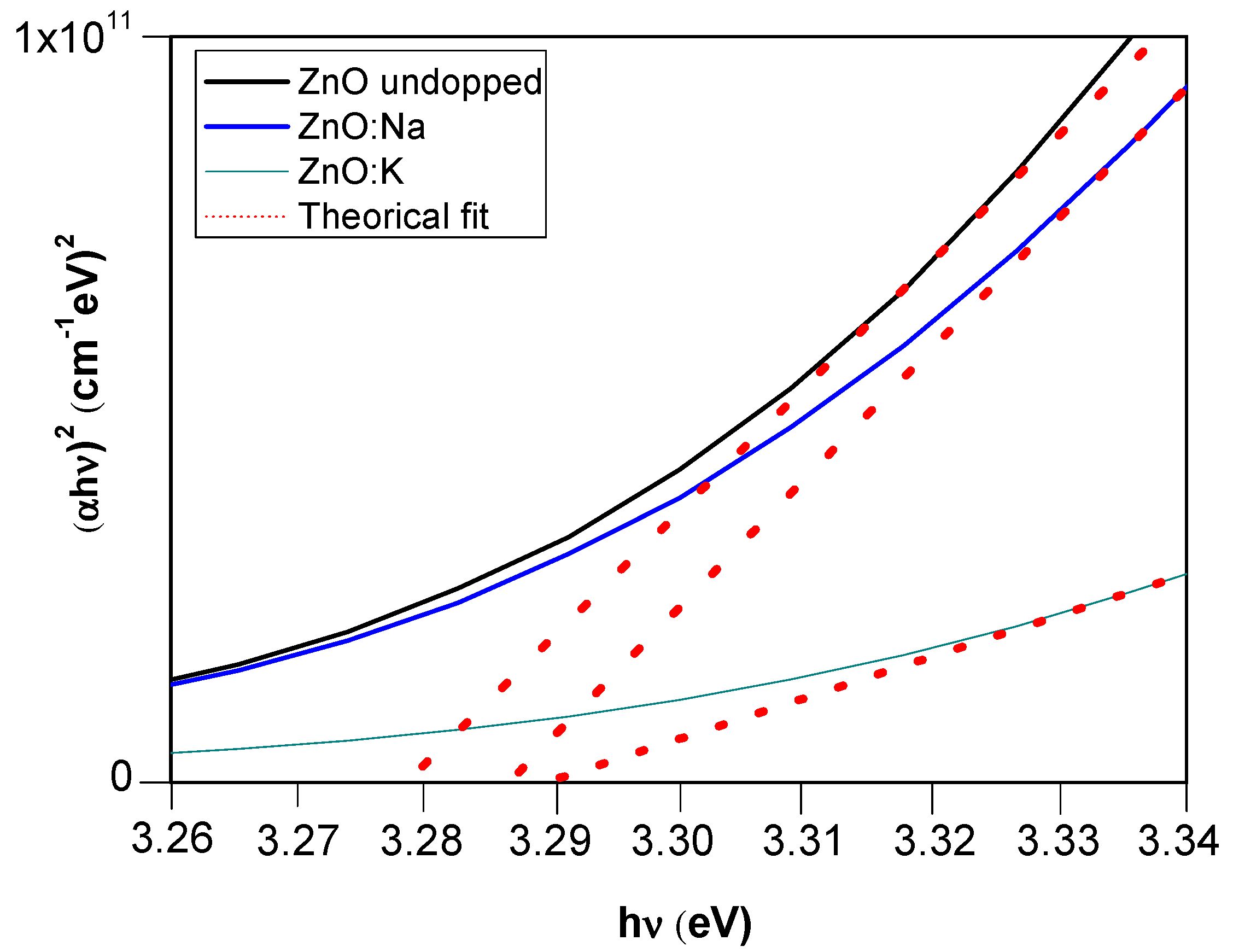
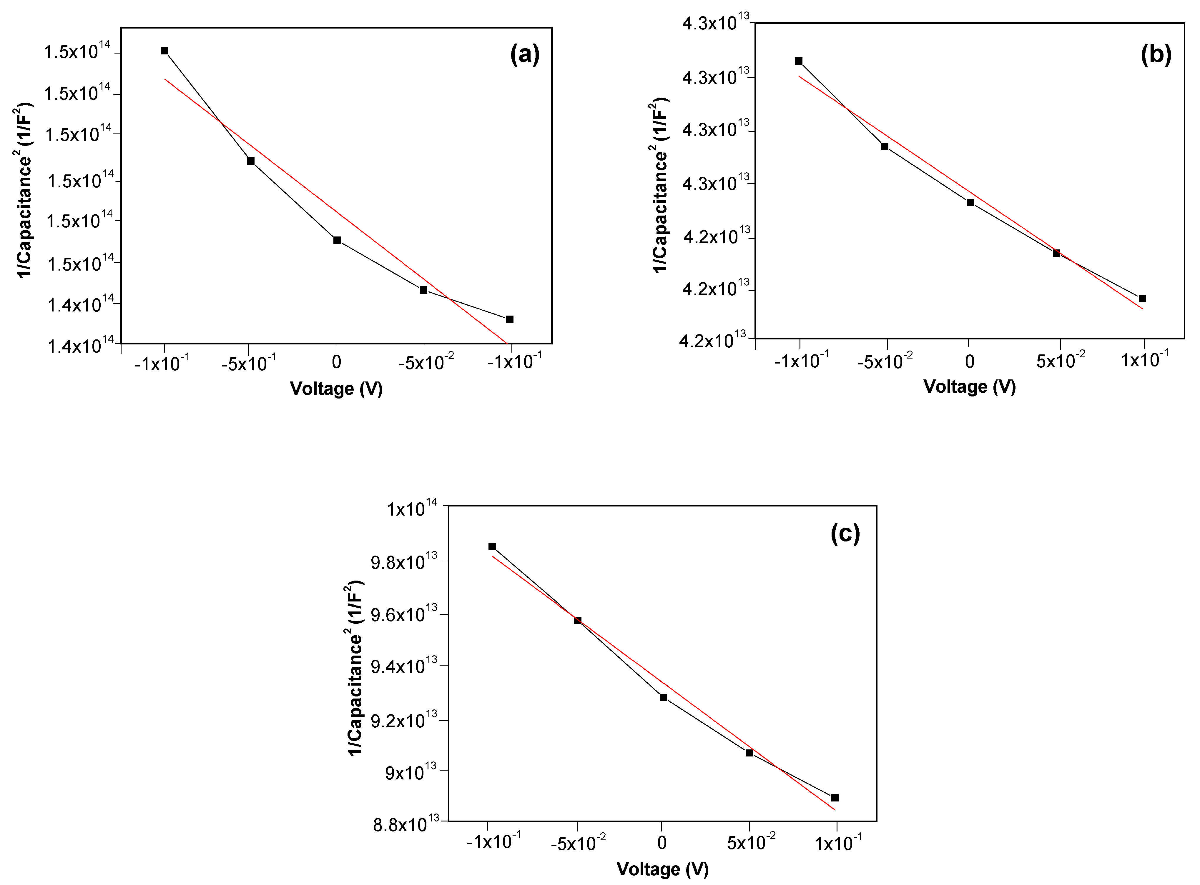
3.3. Optical and Electrical Properties of M-Doped ZnO (M = Na, K) Thin Films

Figure 4 exhibit the optical transmittance spectra of undoped and doped ZnO thin films deposited on a soda-lime substrate. In the visible region with wavelengths ranging from 400 nm to 800 nm, all the samples were highly transparent with the average optical transmittance of 80% and 78% for Na and K dopants, respectively. The crystal dimensions were similar in the three dopants; therefore, the values of the transmittance were related to the thickness of the films when the thickness increased the value of the transmittance decreased.
The absorption coefficient (α) values were calculated using Lambert’s Law as the following equation [39]:
α = 1 t ln ( 1 T )
where t is the film thickness and T is the transmittance. An optical band gap of thin films was estimated using the equation x by the extrapolation of (αhν)2 vs. .
α h v = A ( h v E g ) 1 2
where h v is the photon energy, A is a constant, and Eg is the optical band gap. ZnO, ZnO:Na and ZnO:K films optical band gaps are shown in Figure 5, the energy band gap was determined by extrapolating linear region of the plot to energy axis where α2 = 0 [40].
ZnO thin film presented a wide band gap of 3.28 eV. The optical band gap values of ZnO:Na and ZnO:K thin films were 3.285 and 3.29 eV, respectively. The fitting results show that the energy band gaps increased with an increase in the atomic radio of the dopant and suggests that the band gap could be tuned for the applications in various electronic and optical applications.
Electrical properties of the ZnO films doped with 3% of different alkalines were measured at room temperature using a four-point probe working station are listed in Table 1. The current–voltage characteristics were measured by a digital electrometer and stabilized power supply. The mobility was calculated multiplying the measured resistivity with the doping/carrier density.
The method used a linear sequence of four equally-spaced tips that were pressed on the surface of the material. A small current I from a constant-current source was passed through the outer two probe tips and the voltage drop V was measured between the inner two probe tips. The resistivity values were calculated using the following equation [41]
ρ = C ( V I ) w
where w is the thickness, ρ the resistivity, V the voltage, C is a geometrical correction factor, and I the current. At the limit when the probe tips spacing, s, was much less than the lateral dimension of the sample, C becomes (π/ln2) = 4.54. The following equation gives the electrical conductivity.
σ = 1 ρ
where σ is conductivity.
The samples showed a different value of resistivity, the lowest value was obtained for the ZnO:Na sample. K doping greatly increased the defect creation, and it could act as scattering centers, and it produced an increase in the resistivity because the mobility decreased; therefore, the value of the resistivity of ZnO:K increased [42]. As a result, the presence of the alkali dopants, in our samples, always improved the value of resistivity than that of the undoped ZnO thin film.
The Mott–Schottky equation could be used to determine the flat-band potential and the carrier concentration of the semiconductor. Understanding its derivation was essential for this experiment because it reinforces many key concepts associated with the semiconductor–electrolyte interface. However, the starting point for the derivation is Poisson’s [43].
d 2 Φ d x 2 = ρ ε ε 0
where ρ corresponds to the charge density at a position x away from the semiconductor surface, ε is the dielectric constant of the semiconductor, and ε 0 is the permittivity of free space. Using the Boltzmann distribution to describe the distribution of electrons in the space charge region and Gaus’s law relating the electric field through the interface to the charge contained within that region, Poisson’s equation can be solved to give the Mott–Schottky equation [44,45].
1 C 2 = 2 ε r ε 0 A 2 e N D ( V V f κ B T e )
where C is the capacitance, A is the interfacial area,   N D the number of donors, V the applied voltage, V f is the flat band potential, κ B is Boltzmann’s constant, T the absolute temperature (taken as 298 K), and e is the electron charge, ε 0 is the permittivity in the vacuum, and ε r is the relative permittivity of soda-lime glass (taken as 7.3) [46].
Therefore, a plot of C−2 vs. V (Figure 6) should yield a straight line from which V f can be determined from the intercept on the V axis. The value of N D can also be conveniently found from the slope knowing ε 0   , ε r , and A.
The conduction mechanism could be determined by the polarity carrier concentration. Figure 6 shows that the value of the slope was negative in all the dopants; as a result, the polarity carrier concentration was negative, so it concludes that films are n-type. This linearity deviation in the Mott–Schottky plots may be associated with the polycrystalline nature of the samples and high interface defects. ZnO is considered n-type semiconductor due to a large number of point defects, Zn vacancy or interstitial sites, as well as oxygen vacancy [47]. ZnO could have either Zn interstitial or oxygen vacancy or both, which lead to the excess unpaired electron that enhances n-type conductivity [48]. The oxygen vacancy has frequently been associated as the source of unintentional n-type conductivity, but recent researches indicate that this assignment cannot be correct [49]. However, this is statement is not useful for any elements. Hence, p-type conduction in ZnO requires the incorporation of shallow acceptor levels which may be possible by substituting monovalent atoms (as elements from the group I) at Zn sites that create one hole per alkali atom in the neighboring oxygen atom. However, the literature has reported that group-I elements (Na, K) tend to occupy the interstitial site, thereby acting as a donor, not as an acceptor [48]. Table 1 shows that all the thin films regardless the dopant exhibit n-type conduction, whereas the Na doping n-type conduction may be related to the increase in the donor-like V0 density and the compensation of Nai for the NaZn acceptor. The conduction mechanism for the K doping shows that n-type conduction behavior had arisen due to the preferential occupation of K into the interstitial sites and acted as donors to supply electrons [50]. The samples show electron conduction behavior (n-type) with a carrier concentration in the region of ~1018 cm−3. It is important to note that a solid solution of Na, and K-doped ZnO increase the carrier concentration of the undoped ZnO thin film.

4. Conclusions

We developed very low resistant and highly transparent alkali-doped ZnO thin films for transparent conductive oxide applications by an easy low-cost spray pyrolysis technique. The structural, morphological, optical, and electrical properties of the coating with composition Zn1−x MxO (x = 0.03) were characterized. All samples crystallize in a single hexagonal phase of wurtzite structure with preferred c-axis orientation along a (002) crystal plane. Highly transparent layers were obtained with an average optical transmittance of 80%. The energy band gap of doped ZnO films increased from 3.27 to 3.29 eV by a rising of the atomic number of dopants. The samples show n-type electron conduction behavior with a carrier concentration in the region of ~1018 cm−3. The alkali-doped ZnO films obtained by the easy and low-cost method has great potential for photovoltaics (PV) as interconnecting layer in tandem technology based on the monolithic integration of interdigitated back-contacted c-Si solar cells devices as bottom cells, with wide band-gap semi-transparent kesterite top cells in a four contacts configuration, this being compatible with future industrialization of the technology.

Author Contributions

Conceptualization, J.B.C. and D.F.; methodology, S.P.; software, T.S.-L.; validation, T.S.-L.; investigation, S.P. and J.G.C.; writing—original draft preparation, S.P.; writing—review and editing, D.F. and T.S.-L.; supervision, J.B.C. and D.F.; project administration, J.B.C.; funding acquisition, J.B.C. All authors have read and agreed to the published version of the manuscript.

Funding

Spanish Ministry of Economy and Competitiveness under the program Programa Estatal de I+D+I orientada a los retos de la sociedad in the framing of the IGNITE project (ENE2017-87671-C3-3-R) and Proyecto PID2020-116719RB-C43 financiado por MCIN/AEI/10.13039/501100011033.

Institutional Review Board Statement

Not applicable.

Informed Consent Statement

Not applicable.

Data Availability Statement

Not applicable.

Acknowledgments

The authors would like to acknowledge the financial support of the Spanish Ministry of Economy and Competitiveness under the program Programa Estatal de I+D+i orientada a los retos de la sociedad in the framing of the IGNITE project (ENE2017-87671-C3-3-R) and the program Proyectos de I+D+i» de los Programas Estatales de Generación de Conocimiento y Fortalecimiento Científico y Tecnológico del Sistema de I+D+i y de I+D+i Orientada a los Retos de la Sociedad, en el marco del Plan Estatal de Investigación Científica y Técnica y de Innovación 2017–2020 (Ref. PID2020-116719RB-C43). We also appreciate the characterization assistance of Central Service of Scientific Instrumentation (SCIC) at the University Jaume I. We also thank the group of A. Perez (IREC) and the group of F. Fabregat (INAM-UJI) for the analysis and characterization assistance.

Conflicts of Interest

The authors declare no conflict of interest.

References

  1. Ferhati, H.; Djeffal, F.; Kacha, K.; Bendjerad, A.; Benhaya, A. Influence of TCO intermediate thin-layers on the electrical and thermal properties of metal/TCO/p-Si Schottky structure fabricated via RF magnetron sputtering. Phys. E Low-Dimens. Syst. Nanostruct. 2019, 106, 25–30. [Google Scholar] [CrossRef]
  2. Cruz, A.; Wang, E.C.; Morales-Vilches, A.B.; Meza, D.; Neubert, S.; Szyszka, B.; Schlatmann, R.; Stannowski, B. Effect of front TCO on the performance of rear-junction silicon heterojunction solar cells: Insights from simulations and experiments. Sol. Energy Mater. Sol. Cells 2019, 195, 339–345. [Google Scholar] [CrossRef]
  3. Çolak, H.; Karaköse, E. Tm-DOPED ZnO NANORODS as a TCO for PV Applications. J. Rare Earths 2018, 36, 1067–1073. [Google Scholar] [CrossRef]
  4. Todorov, T.K.; Bishop, D.M.; Lee, Y.S. Materials perspectives for next-generation low-cost tandem solar cells. Sol. Energy Mater. Sol. Cells 2018, 180, 350–357. [Google Scholar] [CrossRef]
  5. Aouaj, M.A.; Diaz, R.; Belayachi, A.; Rueda, F.; Abd-Lefdil, M. Comparative study of ITO and FTO thin films grown by spray pyrolysis. Mater. Res. Bull. 2009, 44, 1458–1461. [Google Scholar] [CrossRef]
  6. Thampy, A.S.; Dhamodharan, S.K. Performance analysis and comparison of ITO-and FTO-based optically transparent terahertz U-shaped patch antennas. Phys. E Low-Dimens. Syst. Nanostruct. 2015, 66, 52–58. [Google Scholar] [CrossRef]
  7. Han, C.H.; Han, S.D.; Gwak, J.; Khatkar, S.P. Synthesis of indium tin oxide (ITO) and fluorine-doped tin oxide (FTO) nano-powder by sol-gel combustion hybrid method. Mater. Lett. 2007, 61, 1701–1703. [Google Scholar] [CrossRef]
  8. Bisht, H.; Eun, H.T.; Mehrtens, A.; Aegerter, M.A. Comparison of spray pyrolyzed FTO, ATO and ITO coatings for flat and bent glass substrates. Thin Solid Films 1999, 351, 109–114. [Google Scholar] [CrossRef] [Green Version]
  9. Kawashima, T.; Matsui, H.; Tanabe, N. New transparent conductive films: FTO coated ITO. Thin Solid Films 2003, 445, 241–244. [Google Scholar] [CrossRef]
  10. Cho, S.W.; Kim, Y.B.; Kim, D.E.; Kim, K.S.; Yoon, Y.D.; Kang, W.J.; Lee, W.; Cho, H.K.; Kim, Y.H. The pH-dependent corrosion behavior of ternary oxide semiconductors and common metals and its application for solution-processed oxide thin film transistors circuit integration. J. Alloy. Compd. 2017, 714, 572–582. [Google Scholar] [CrossRef]
  11. Aydogan, S.; Yilmaz, M. Crystallographic disorders depending on monovalent cations addition and their effects on ZnO’s characteristics. Ceram. Int. 2020, 46, 8420–8430. [Google Scholar] [CrossRef]
  12. Baruah, S.; Dutta, J. Hydrothermal growth of ZnO nanostructures. Sci. Technol. Adv. Mater. 2009, 10, 013001. [Google Scholar] [CrossRef]
  13. Mahmood, A.; Naeem, A. Sol-Gel-Derived Doped ZnO Thin Films: Processing, Properties, and Applications. In Recent Applications in Sol-Gel Synthesis; Intech Open: London, UK, 2017; pp. 169–193. [Google Scholar] [CrossRef] [Green Version]
  14. Kegel, J.; Povey, I.M.; Pemble, M.E. Zinc oxide for solar water splitting: A brief review of the material’s challenges and associated opportunities. Nano Energy 2018, 54, 409–428. [Google Scholar] [CrossRef]
  15. Marouf, S.; Beniaiche, A.; Kardarian, K.; Mendes, M.J.; Sanchez-Sobrado, O.; Águas, H.; Fortunato, E.; Martins, R. Low-temperature spray-coating of high-performing ZnO:Al films for transparent electronics. J. Anal. Appl. Pyrolysis 2017, 127, 299–308. [Google Scholar] [CrossRef]
  16. Ynineb, F.; Attaf, N.; Aida, M.S.; Bougdira, J.; Bouznit, Y.; Rinnert, H. Morphological and optoelectrical study of ZnO:In/p-Si heterojunction prepared by ultrasonic spray pyrolysis. Thin Solid Films 2017, 628, 36–42. [Google Scholar] [CrossRef]
  17. Mondal, P.; Das, D. Further improvements in conducting and transparent properties of ZnO:Ga films with perpetual c-axis orientation: Materials optimization and application in silicon solar cells. Appl. Surf. Sci. 2017, 411, 315–320. [Google Scholar] [CrossRef]
  18. Seawsakul, K.; Horprathum, M.; Eiamchai, P.; Pattantsetakul, V.; Limwichean, S.; Muthitamongkol, P.; Thanachayanont, C.; Songsiriritthigul, P. Glancing-angle pulsed dc magnetron sputtered AZO thin films for TCO applications. Mater. Today Proc. 2018, 5, 14166–14171. [Google Scholar] [CrossRef]
  19. Wu, J.; Wang, Z.; Chen, F.; Shen, Q.; Zhang, L. Chemical evolution of target surfaces during RF magnetron sputtering and its effect on the performance of TCO films. Appl. Surf. Sci. 2019, 493, 665–672. [Google Scholar] [CrossRef]
  20. Bedia, A.; Bedia, F.Z.; Aillerie, M.; Maloufi, N. Structural, electrical and optical properties of Al–Sn codoped ZnO transparent conducting layer deposited by spray pyrolysis technique. Superlattices Microstruct. 2017, 111, 714–721. [Google Scholar] [CrossRef]
  21. Ye, Z.; Wang, T.; Wu, S.; Ji, X.; Zhang, Q. Na-doped ZnO nanorods fabricated by chemical vapor deposition and their optoelectrical properties. J. Alloy. Compd. 2017, 690, 189–194. [Google Scholar] [CrossRef]
  22. Li, Y.; Zhang, Y.; He, H.; Ye, Z.; Jiang, J.; Cao, L. Growth of Na doped p-type non-polar a-plane ZnO films by pulsed laser deposition. Mater. Lett. 2012, 76, 81–83. [Google Scholar] [CrossRef]
  23. Tay, C.B.; Chua, S.J.; Loh, K.P. Stable p-type doping of ZnO film in aqueous solution at low temperatures. J. Phys. Chem. C 2010, 114, 9981–9987. [Google Scholar] [CrossRef]
  24. Zhang, J.; Tse, K.; Wong, M.; Zhang, Y.; Zhu, J. A brief review of co-doping. Front. Phys. 2016, 11, 117405. [Google Scholar] [CrossRef] [Green Version]
  25. Bu, I.Y.Y. Direct formation of p-type ZnO by using potassium hydroxide. Optik 2018, 159, 87–93. [Google Scholar] [CrossRef]
  26. Kaneva, N.; Stambolova, I.; Blaskov, V.; Dimitriev, Y.; Bojinova, A.; Dushkin, C. A comparative study on the photocatalytic efficiency of ZnO thin films prepared by spray pyrolysis and sol-gel method. Surf. Coat. Technol. 2012, 207, 5–10. [Google Scholar] [CrossRef]
  27. Zhao, J.L.; Li, X.M.; Zhang, S.; Yang, C.; Gao, X.D.; Yu, W.D. Highly (002)-oriented ZnO film grown by ultrasonic spray pyrolysis on ZnO-seeded Si (100) substrate. J. Mater. Res. 2006, 21, 2185–2190. [Google Scholar] [CrossRef] [Green Version]
  28. Murti, D.K.; Bluhm, T.L. Preferred orientation of ZnO films controlled by r.f. sputtering. Thin Solid Films 1982, 87, 57–61. [Google Scholar] [CrossRef]
  29. Janotti, A.; Van De Walle, C.G. Fundamentals of zinc oxide as a semiconductor. Rep. Prog. Phys. 2009, 72, 126501. [Google Scholar] [CrossRef] [Green Version]
  30. Erhart, P.; Albe, K. First-principles study of migration mechanisms and diffusion of oxygen in zinc oxide. Phys. Rev. B 2006, 73, 115207. [Google Scholar] [CrossRef] [Green Version]
  31. Ilican, S. Effect of Na doping on the microstructures and optical properties of ZnO nanorods. J. Alloy. Compd. 2013, 553, 225–232. [Google Scholar] [CrossRef]
  32. Guan, S.; Watabe, T.; Hao, L.; Yoshida, H.; Cheng, Y.; Zhou, K.; Lu, Y. Enhanced photocatalytic activity of potassium-doped titania photocatalyst films with nanosheet structure. Mater. Lett. 2019, 242, 174–178. [Google Scholar] [CrossRef]
  33. Purbayanto, M.A.K.; Rusydi, A.; Darma, Y. The effect of crystallinity on the surface modification and optical properties of ZnO thin films. Phys. Chem. Chem. Phys. 2020, 22, 2010–2018. [Google Scholar] [CrossRef]
  34. Chen, M.; Wang, X.; Yu, Y.H.; Pei, Z.L.; Bai, X.D.; Sun, C.; Huang, R.F.; Wen, L.S. X-ray photoelectron spectroscopy and auger electron spectroscopy studies of Al-doped ZnO films. Appl. Surf. Sci. 2000, 158, 134–140. [Google Scholar] [CrossRef]
  35. Hsieh, P.T.; Chen, Y.C.; Kao, K.S.; Wang, C.M. Luminescence mechanism of ZnO thin film investigated by XPS measurement. Appl. Phys. A 2008, 90, 317–321. [Google Scholar] [CrossRef]
  36. Szörényi, T.; Laude, L.D.; Bertóti, I.; Kántor, Z.; Geretovszky, Z. Excimer laser processing of indium-tin-oxide films: An optical investigation. J. Appl. Phys. 1995, 78, 6211–6219. [Google Scholar] [CrossRef]
  37. Ratana, T.; Amornpitoksuk, P.; Ratana, T.; Suwanboon, S. The wide band gap of highly oriented nanocrystalline Al doped ZnO thin films from sol-gel dip coating. J. Alloy. Compd. 2009, 470, 408–412. [Google Scholar] [CrossRef]
  38. Qiu, J.; Guo, B.; Zhang, H.; Yu, C.; Li, F. Insights into Working Mechanism of Alkali Metal Fluorides as Dopants of ZnO Films in Inverted Polymer Solar Cells. J. Phys. Chem. C 2018, 122, 24542–24549. [Google Scholar] [CrossRef]
  39. Smits, F.M. Measurement of Sheet Resistivities with the Four-Point Probe. Bell Syst. Tech. J. 1958, 37, 711–718. [Google Scholar] [CrossRef]
  40. Kim, S.K.; Kim, S.A.; Lee, C.H.; Lee, H.J.; Jeong, S.Y.; Cho, C.R. The structural and optical behaviors of K-doped ZnO/Al2O3 (0001) films. Appl. Phys. Lett. 2004, 85, 419–421. [Google Scholar] [CrossRef]
  41. Gelderman, K.; Lee, L.; Donne, S.W. Flat-band potential of a semiconductor: Using the Mott-Schottky equation. J. Chem. Educ. 2007, 84, 685–688. [Google Scholar] [CrossRef]
  42. Pedemonte, M.M. Estudios Fisicoquímicos Sobre Materiales Basados enel TiO2 Relacionados con la Foto-Descomposición de Agua y el Desarrollo de Celdas Solares Foto-Electroquímicas. Ph.D. Thesis, Universidad Nacional de La Plata, Provincia de Buenos Aires, Argentina, 2011. [Google Scholar]
  43. Singh, B.K.; Tripathi, S. Performance analysis of Schottky diodes based on Bi doped p-ZnO thin films. Superlattices Microstruct. 2018, 120, 288–297. [Google Scholar] [CrossRef]
  44. Le Bourhis, E. Glass: Mechanics and Technology, 2nd ed.; Wiley: Hoboken, NJ, USA, 2014. [Google Scholar] [CrossRef]
  45. Reeber, R.R. Lattice parameters of zno from 4.2 to 296 k. J. Appl. Phys. 1970, 41, 5063–5066. [Google Scholar] [CrossRef]
  46. Van De Walle, C.G. Hydrogen as a cause of doping in zinc oxide. Phys. Rev. Lett. 2000, 85, 1012–1015. [Google Scholar] [CrossRef] [PubMed] [Green Version]
  47. Stamataki, M.; Tsamakis, D.; Xanthakis, J.P.; Ali, H.A.; Esmaili-Sardari, S.; Iliadis, A.A. Electrical characterization of Cr Schottky contacts on undoped and Ni-doped p-ZnO films grown by pulsed laser deposition on Si (1 0 0) substrates. Microelectron. Eng. 2013, 104, 95–99. [Google Scholar] [CrossRef]
  48. Akcan, D.; Gungor, A.; Arda, L. Structural and optical properties of Na-doped ZnO films. J. Mol. Struct. 2018, 1161, 299–305. [Google Scholar] [CrossRef]
  49. Zhang, G.; Pan, C.; Zhou, Q. Effects of doping Na on the structure and physical properties of La2/3Ca1/3MnO3. Solid State Commun. 2007, 141, 471–473. [Google Scholar] [CrossRef]
  50. Xu, L.; Li, X.; Yuan, J. Effect of K-doping on structural and optical properties of ZnO thin films. Superlattices Microstruct. 2008, 44, 276–281. [Google Scholar] [CrossRef]
Figure 1. X-ray diffraction patterns of undoped, Na-doped, and K-doped ZnO thin films.
Solar 01 00004 g001
Figure 2. Cross-section images (a) ZnO, (b) ZnO:Na, and (c) ZnO:K thin films.
Solar 01 00004 g002
Figure 3. (a) XPS spectra of the Zn 2p 3/2 in the undoped ZnO, ZnO:Na 3%, and ZnO:K 3% films. (b) XPS spectrum and simulated lines of Na 1s in the ZnO:Na 3%. (c) XPS spectrum of the K 2p in ZnO:K 3%. (d) Oxygen 1s spectra of ZnO, ZnO:Na, and ZnO:K thin films.
Solar 01 00004 g003
Figure 4. Optical transmittance and absorption spectra of M-Doped ZnO thin films.
Solar 01 00004 g004
Figure 5. Relation of (αhv)2 and hv of M-doped ZnO thin films. ZnO, ZnO:Na, and ZnO:K.
Solar 01 00004 g005
Figure 6. Mott−Schottky plots of the capacitance of (a) ZnO, (b) ZnO:Na, and (c) ZnO:K onto soda-lime glass.
Solar 01 00004 g006
Table 1. Electrical properties of M-doped ZnO thin films.
Dopants
(at 3%)
Resistivity
(Ωcm)
Mobility
(cm2 /Vs)
Carrier Concentration (cm−3)Conduction Type
Undoped ZnO1.03 × 10−11 × 1025 × 1017n
Na3.18 × 10−21 × 1021 × 1018n
K5.64 × 10−29 × 1011 × 1018n
Publisher’s Note: MDPI stays neutral with regard to jurisdictional claims in published maps and institutional affiliations.

