Review

Two-Dimensional Ferroelectrics: A Review on Applications and Devices

by
Gabriella Maria De Luca
1,2,* and
Andrea Rubano
1
1
Dipartimento di Fisica “E. Pancini”, Università Federico II, Monte S. Angelo, Via Cintia, 80126 Napoli, Italy
2
Consiglio Nazionale delle Ricerche, Istituto CNR-SPIN, Complesso Universitario di Monte Sant’Angelo, Via Cintia, 80126 Napoli, Italy
*
Author to whom correspondence should be addressed.
Solids 2024, 5(1), 45-65; https://doi.org/10.3390/solids5010004
Submission received: 8 November 2023 / Revised: 8 January 2024 / Accepted: 10 January 2024 / Published: 16 January 2024
(This article belongs to the Special Issue Recent Advance in Ferroelectric Composites)

Abstract

:
Over the last few years, research activities have seen two-dimensional (2D) materials become protagonists in the field of nanotechnology. In particular, 2D materials characterized by ferroelectric properties are extremely interesting, as they are better suited for the development of miniaturized and high-performing devices. Here, we summarize the recent advances in this field, reviewing the realization of devices based on 2D ferroelectric materials, like FeFET, FTJ, and optoelectronics. The devices are realized with a wide range of material systems, from oxide materials at low dimensions to 2D materials exhibiting van der Waals interactions. We conclude by presenting how these materials could be useful in the field of devices based on magnons or surface acoustic waves.

1. Introduction

Ferroelectricity in Rochelle salt was discovered in 1921 by J. Valasek [1], with the sign of spontaneous polarization (P s ) being controllable by an external electric field. Since this discovery, many efforts have been made to enhance technological applications, such as field-effect transistors (FeFET) [2], sensors [3], photonic devices [4], and optoelectronics [5]. However, the constant demand for higher-performance devices has necessitated increased efforts toward miniaturization in nanoelectronics, and consequently, toward the preparation of thin and ultra-thin ferroelectric films. In 2018, H. Wang et al. [6] demonstrated through the first-principles calculation and Kelvin probe microscopy that in BiFeO 3 thin films, the critical thickness for ferroelectric response can vanish, making this compound a promising candidate for high-density non-volatile memories. Recently, J. Muller et al. [7] succeeded in demonstrating the significant potential of FeFET scaling (based on Fe-HfO 2 ) in advanced nodes, when HfO 2 is integrated into 28 nm high-k metal gate (HKMG) technology. Nevertheless, in all oxide thin films, a non-uniform concentration of oxygen vacancies at the interface can lead to suboptimal FeFET device performance, such as the wake-up effect and/or an increase in leakage current [8]. While these results are amazing for technological applications, achieving a ferroelectric (FE) response as we approach the 2D limit remains challenging. Therefore, while it is important to improve the synthesis of ultra-thin FE films to avoid surface dangling bonds and lattice mismatch, the discovery of 2D van der Waals (VdW) FE materials has overcome these limitations, enabling VdWs to be strong candidates in the realization of heterostructure-based devices with atomically sharp interfaces. In 1976, the existence of 2D FE was predicted [9], but the first experimental confirmation did not arrive until 2015 [10]. Observing both in-plane (IP) and out-of-plane (OP) polarization in few-unit-cells-thick materials was indeed a big challenge. For example, Chang et al. observed only an IP polarization in SnTe [11], while an OP polarization was found in the room-temperature 2D ferroelectric CuInP 2 S 6 [12]. It was only in 2018 that the locking between IP and OP ferroelectric polarization was observed in 2D In 2 Se 3 [13], leading to the exploration of 2D multiferroics, where more than one ferroic order is present. To date, the list of 2D VdW ferroelectric materials is quite extensive, ranging from inorganic [14,15,16,17] to hybrid organic–inorganic perovskite ferroelectrics (HOIPFs) [18], and electronic devices based on 2D FE materials have been realized. Particular attention to 2D VdW ferroelectric materials arises from their semiconducting nature, not observed in traditional perovskite ferroelectrics, which are generally insulators, leading to new perspectives in the realization of FeFET devices, thanks to the high carrier mobility typical of semiconductors. However, the field of 2D materials is largely unexplored; many theoretical predictions have been made on the wide spectrum of electronic properties in 2D VdW ferroelectric materials, exhibiting a Curie temperature value close to room temperature [19], and unique photonic and optoelectronic properties, thanks to the wide range of band gaps covering everything from deep ultraviolet rays to microwaves of the electromagnetic spectrum. All these properties are key for modern research and technology applications. In this review, we discuss some recent developments of ferroelectric devices based on 2D materials [20]; see Figure 1. In Section 2, we introduce the theory of 3D and 2D ferroelectricity, while Section 3 discusses strategies and mechanisms used for integrating 2D materials in FeFET and FTJ devices. Section 4 and Section 5 focus on optical devices and non-standard applications, respectively. In Section 10, we outline the future challenges for developing better 2D ferroelectric/multiferroic devices.

2. Theoretical Background

For a material to be ferroelectric, it must have a non-centrosymmetric crystal structure, a spontaneous switchable electric polarization (P) when an electric field (E) is applied, and, last but not least, the presence of a unique polar axis. The ferroelectric response is characterized by P-E hysteretic loops, where the values of remnant polarization (P s ) and the coercive field (E c ) are determined; these loops disappear above a critical temperature. P s and E c become extremely important in determining the operation voltage and memory window, which are necessary for the characterization of memory devices [12,21,22]. However, when a ferroelectric material is thinned to a quasi-2D form, it may exhibit some new behaviors that could depend on its size. These new properties can affect how the 2D material behaves as a ferroelectric, consequently making it different from its 3D counterpart. Moreover, transitioning to a pure 2D regime, we observe a different scenario. As demonstrated by Mermin and Wagner [23] for pure 2D ferromagnetic and antiferromagnetic systems, the symmetry of continuity is broken. This implies that in a pure 2D system with a flat surface, free of distortions or dislocations, ferroelectricity is forbidden. The reason is that transitioning from 3D to 2D weakens the long-range order and decreases the critical temperature, which in turn makes thermal fluctuations larger than the potential barrier, hindering ferroelectricity. However, with 2D VdW materials, we are at the limit of the 2D regime: here, the presence of weak chemical bonds favors weak interactions, consequently allowing long-range ordering and, thus, ferroelectricity. Moreover, 2D VdW materials possess several properties that may aid in maintaining ferroelectric polarization, such as a stable surface and the ease of functionalizing surface atoms. From DFT calculations and experiments, it has been observed that, similar to 3D materials, the FE polarization can have different origins in the 2D limit as well.
In 3D BaTiO 3 and PbTiO 3 , polarization is due to the ionic displacement of of Ti 4 + ions, driven by the hybridization of Ti-3d and O-2p orbitals; this is similar to what is observed in 2D SnTe, where the intra-layer displacement between Sn and Te ions induces a lattice distortion from cubic to rhombohedral [24]. Recently, ionic displacement responsible for spontaneous polarization was also observed in hybrid organic-inorganic perovskite ferroelectrics (HOIPFs) materials [18]. HOIPFs have attracted a great deal of attention from researchers because, even though the polarization in the inorganic part is driven by ionic displacement, it is not mutually exclusive with the polarization induced in the molecular (organic) part due to the presence of a permanent dipole moment. Most of the HOIPF materials are Pb-based. These materials are mainly used in photovoltaics and photodetection [25]. However, research is advancing toward new lead-free technologies, and in this context, HOIPF materials also show interesting results. In Figure 2, an excellent piezoelectric response is shown in TMCM-MnCl 3 [18]. Although some details are not yet clear, first-principle calculations show that the spin texture can be tuned by external fields [26], thus demonstrating the technological potential of this hybrid organic–inorganic system. In addition, if polarization results from the product of other electronic ordering (charge, orbital, or magnetic), it leads to improper ferroelectricity, as seen in TbMnO 3 (TMnO) [27], a typical II-type multiferroic. Multiferroic materials are characterized by more than one ferroic order: in the case of TMnO, ferroelectricity is created by spin-driven polarization, similar to what happens in monolayer Ni 2 , where spin chirality generates a finite electric polarization. Due to their characteristics, multiferroics are increasingly being researched for new nanoelectronic applications, aiming to develop reversible systems. This is due to the magnetoelectric coupling, which allows the control of magnetic properties by an external electric field and vice versa.
In the following sections, we will discuss how 3D oxides in the 2D limit, 2D VdW ferroelectrics, 2D multiferroics, and HOIPFs have modified the approach to engineering devices like FeFET, FTJ optoelectronics, surface acoustic waves, and magnon electronics.

3. FeRAM Devices

James F. Scott is considered the father of ferroelectric devices [28], and even after many years, ferroelectric materials remain a hot research topic, especially considering advancements in miniaturization. New applications such as big data, the internet of things, artificial intelligence, wearable electronics, and more, require increasingly high computing power in various forms. The celebrated Moore’s law predicts that the number of transistors, a quantity that strongly correlates with computing power, on a single chip will grow exponentially [29]. Therefore, digital computation needs fast, low-power switches that can be packed densely on a chip. This has been achieved by lowering the supply voltages and shrinking the size of silicon transistors with various material and structural innovations. Today, silicon transistors are becoming harder and more expensive to scale down, and they will eventually reach their physical limits when the channel length is close to atomic scales [30,31]. The best possible strategy is to go beyond CMOS transistors, searching for other kinds of switches that can process information faster and/or more efficiently. Many options, such as spin FETs, tunnel FETs, negative capacitance (NC) FETs, nanoelectromechanical (NEM) switches, and memristor devices, are under active research [32,33]. Recently, different memory technologies based on ferroelectric materials have been studied, like ferroelectric rapid access memory (FeRAM), ferroelectric field effect (FeFET) devices, and ferroelectric tunnel junction (FTJ). These memory devices offer many advantages, such as fast writing/reading speed, long-lasting data retention, high durability, and low energy consumption for writing. These excellent features suggest that they can be used to create high-performance synaptic devices for neuromorphic computing.
FeRAM is characterized by a metal-ferroelectric-metal (MFM) stack and utilizes the polarization switching of the ferroelectric material. When an external voltage is applied to the MFM stack, ferroelectric switching is observed due to the dipoles in the ferroelectric layer changing direction. Unfortunately, this type of technology has a significant drawback: to read the memory state, the device has to be erased, and the memory state depends on the amount of polarization charge on the ferroelectric capacitor. These capacitors are expected to become smaller with improving technology, leading to many efforts to find alternatives. FeFET and FTJ have been studied, where the memory state can be read without erasing it, and the memory cell size can be easily reduced. The switching of polarization in FeFET can be obtained by applying an external electric field: a FeFET is a device that has a ferroelectric layer on top of a transistor. By applying a high-voltage pulse to the gate of the FeFET, the ferroelectric layer can be polarized in two directions. One direction helps turn the transistor on, and the other helps turn it off. This changes the voltage needed to switch the transistor, which can therefore be used to store information in the FeFET without destroying it. However, to make a good and small FeFET, we need to consider two things: first, the switching voltage depends on how difficult it is to change its polarization and its thickness; second, the gate voltage is not only applied to the ferroelectric layer but also to another insulator layer in the gate stack (see Figure 3). This means that there is always some electric field in the ferroelectric layer, even when there is no gate voltage. This electric field opposes the polarization of the ferroelectric layer and makes it weaker over time. This affects how long the information can be stored in the FeFET and how many times it can be rewritten. To improve the device, we need to choose an insulator layer that has high capacitance and a ferroelectric layer that has low capacitance. In this way, most of the gate voltage goes to the ferroelectric layer and not to the insulator layer. The problem with usual ferroelectric materials is that they are not hard enough and not thin enough, so they need a relatively high voltage to switch.
Perovskite-based FeFETs are commonly used, but they cannot laterally scale down below 180 nm. Indeed, a large thickness of the ferroelectric is needed to balance the memory window, due to low coercive fields E c [35]. FE-HfO 2 offers a solution to this problem: it has a high Ec of 1–2 MV/cm and can be scaled down in thickness [36]. In the next paragraph, we will review this particular type of FeFET in more detail.

4. FeFET-Oxides/2D VdW

When building a FeFET, we have to consider the longevity of the memory capacity. Indeed, how much memory is lost when the device is not in use, how the gate voltage is spread, and how much charge is injected when writing data depend on the capacitive voltage divider. This means that to make memory last longer and work better, the best option is, as mentioned before, to have a high capacitance for the insulator and low capacitance for the ferroelectric material. FeFETs based on FE-HfO 2 can scale down better than perovskite-based ones. This is because FE-HfO 2 has low permittivity [36,37], showing a fast switching spread (≤100 ns), switching voltages between 4 and 6 V, and data retention for 10 years. However, for cycling endurance, the problem is that Fe-HfO 2 has a high E c , making the electric field in the insulator very strong. This causes charge trapping when writing data, primarily causing reduced data retention, especially with a very thin interfacial layer [38]. However, recently, Tan et al. [39] demonstrated that even in this compound, it is possible to achieve an endurance exceeding 10 10 cycles. Despite the promising results shown by oxide-based perovskite FETs, the scalability in terms of size and therefore of an ever-increasing density of devices have made 2D materials increasingly important in the realization of FeFETs. Some materials have very thin layers that can be peeled off, like graphene, transition-metal dichalcogenides (TMDCs), and black phosphorus (BP). These are called two-dimensional (2D) materials. They have amazing properties for structures, electronics, and optoelectronics [40]. They can help improve the performance and functionality of conventional perovskite FeFETs.
For example, Wang et al. made a FeFET with Bi 4 Ti 3 O 12 characterized by a regular stacking of fluorite-like [Bi 2 O 2 ] ( 2 + ) slabs and perovskite blocks [A ( n 1 ) B n O ( 3 n + 1 ) ] ( 2 ) (with n = 3) where the integer n indicates the number of BO 6 octahedra that share corners and form ABO 3 -type perovskite blocks [34,41]. They used this device to mimic a biological synapse (see Figure 3). Indeed, the device can store different levels of conductance that fade over time when exposed to light. This can be used for efficient vector–matrix multiplication. Du et al. [42] also used a FeFET with MoS 2 and BaTiO 3 (perovskite) for neuromorphic vision sensors. The device can sense different wavelengths of light and maintain the conductance after the light is turned off. It is more sensitive to 450 nm of light than to 532 or 650 nm of light. This feature can be utilized for processing visual information (more details on optical properties are given in the next paragraph). Recently, Puebla et al. found that the poling of the BaTiO 3 layer is crucial for the hysteretic behavior to perform electrical measurements as a function of temperature. The hysteresis almost disappears when the temperature is close to the transition from the ferroelectric to the paraelectric phase [43].

5. FTJ-Oxides/2D VdW

On the other hand, the FTJ is a device that consists of a very thin layer of ferroelectric material between two electrodes, or interfaces, which are different. The switching of polarization, by applying an electric field, changes the barrier height that electrons must cross when tunneling through the device. This barrier height affects the device’s resistance, which can be either high or low, depending on the polarization direction. This is known as the resistive switching effect, and it can be used to store information in the FTJ without destroying it. The tunneling electroresistance (TER) effect measures the change in resistance when the polarization is switched. It is usually between 10 and 100 times [44]. There are two ways to achieve a very high TER: the first is to use a barrier with strong electric polarization, and the second is to use a material (like a semiconductor) as the electrode, thereby modulating the barrier width and thickness through field-induced carrier depletion. A good FTJ is expected to show a retention time of up to 10 years and a very high cycling endurance of >10 14 . Recently, researchers have found ways to significantly increase TER, to more than 10 4 . One way is to use BiFeO 3 as the ferroelectric, which has a much larger polarization [45,46]. However, to improve FTJs for scaling, the ferroelectric layer should be very thin. Even in this case, the implementation of 2D materials with perovskite oxides in FTJ has been studied. Li et al. made an FTJ with MoS 2 as a semiconductor electrode and BaTiO 3 as a ferroelectric layer [47]. The polarization of BaTiO 3 can change the band alignment and the carrier properties of MoS 2 , significantly varying the tunneling current. MoS 2 can change its conductivity more than graphene when the polarization of BaTiO 3 switches, resulting in a very high ON/OFF ratio of 10 4 . The FTJ also depends on the interface between BaTiO 3 and MoS 2 . Some molecules can affect the polarization of BaTiO 3 because the interface with MoS 2 is generally realized under ambient conditions. So, if NH 3 molecules make the polarization more stable, H 2 O molecules (a layer of water at the interface) make it less stable. As we have reported before, 2D materials seem to play an important role in the development of new devices. In particular, research is focused on 2D VdW ferroelectric materials, due to their very thin layers, ability to switch polarization with electric fields, and special structure that makes them easy to stack together. This makes them ideal for FeFET and FTJ devices. Many 2D materials have been predicted to possess this property theoretically, but only a few have been confirmed experimentally. About ten 2D ferroelectric materials have been tested thus far: WTe 2 , d1T-MoTe 2 , SnTe, CIPS, BA 2 PbCl 4 , α -In 2 Se 3 , β -In 2 Se 3 , 2H α -In 2 Se 3 , SnSe, and SnS [11,12,48,49,50,51,52,53].
Generally, the performances of FeFET and FTJ can differ depending on whether we have a two- or three-terminal device (see Figure 4). In the following, the differences between these two types of devices are described, with an emphasis on how 2D VdW ferroelectrics can be utilized to enhance device performance.
Two-terminal devices with 2D ferroelectrics feature the FE layer sandwiched between two electrodes. The polarization in the FE layer depends on the voltage pulse applied to the top electrode. For example, if the pulse is positive, the polarization points downward, attracting the negative electrons in the substrate to the interface and making the depletion width smaller, as shown in Figure 5a. On the contrary, when the pulse is negative, the polarization points upward and repels the electrons in the substrate away from the interface, making the depletion width larger, as shown in Figure 5b. The bound charges at the interface are not fully screened by the electrons, creating a depolarization field that opposes the polarization. This leads to energy band bending at the interface, as shown in Figure 5. The potential barrier should be higher when the pulse is negative than when it is positive. This implies that electrons can cross the depletion region more easily when the pulse is positive, due to the lower barrier and narrower width, switching the device to a low-resistance state. When negative pulses are applied repeatedly, the device will develop an opposite polarization that grows larger over time. This will increase the depletion width and barrier height, leading to higher resistance. Conversely, the device will start with upward polarization and high resistance when it receives negative pulses. Then, if positive pulses are applied, the resistance will decrease as the amplitude of the positive pulses increases. This demonstrates how FE polarization affects the depletion width and potential barrier height, creating memristive behavior in the sandwich structure.
The three terminals of FeFET devices are the gate, source, and drain, and they offer some advantages over two-terminal devices; three-terminal FeFETs can write and read data in different ways, making it easier to adjust their power consumption. When spikes are applied, the electric field changes the direction of the polarization domains in the ferroelectric film. The polarization domains change increasingly as more spike pulses are applied. This affects the number of electrons in the channel region, which in turn alters the channel conductivity. Many researchers have utilized 2D materials for the channel to create FeFETs that can function like synapses. They combined 2D materials with various types of ferroelectrics, such as conventional ones (Zr-doped HfO 2 , P(VDF-TrFE), PZT) or 2D ones (CIPS and α -In 2 Se 3 ). Next, we will review some of the latest three-terminal ferroelectric memory devices based on 2D materials, and how they change performance compared to two-terminal devices [55,56,57,58,59].

6. 2D VdW-2 Terminals Devices

α -In 2 Se 3 is a material that has both IP and OP ferroelectricity, meaning it can have electric polarization in different directions. It retains this property even when it is very thin, down to a single layer, and can operate at high temperatures above 200 °C [13,51,60,61,62]. It also has a semiconductor bandgap of about 1.39 eV, which makes it suitable for photodetection [63]. With its excellent optoelectronic properties, it can be used to create photo-transistors with a high gain of about 10 5 A/W [64]. Because of these features, α -In 2 Se 3 can be used in various devices, such as FeFETs, where it acts as the ferroelectric gate layer, FeFETs, where it acts as the ferroelectric semiconductor (FS), and FS junctions, where it forms a junction with another semiconductor, like β -Ga 2 O 3 [65]. Liu et al. [66] developed photodetectors with ferroelectric reconfigurable dark current and responsivity based on α -In 2 Se 3 . By using both the ferroelectric and semiconductor properties of α -In 2 Se 3 , combining three-terminal FeFETs into a two-terminal device structure with crossbar geometry, the device showed memristive behavior, where the conductance was controlled by changing the height of the Schottky barrier induced by the OP ferroelectric polarization (Figure 6). They found that the dark current could be reduced by 50 times from 660 nA in the P u p state to 14 nA in the P d o w n state. The responsivity can also be adjusted accordingly from 5 to 241 A/W. Moreover, they observed that the α -In 2 Se 3 FSJs have excellent optoelectronic properties, such as a fast response speed of 43 μ s and a wide response spectrum from visible to 980 nm.
Another widely studied 2D FE material is CuInP 2 S 6 (CIPS). Its crystal structure is characterized by Cu and In cations filling the octahedral sulfur cages, with P–P pairs occupying the voids (see Figure 7). CIPS has been reported to exhibit room-temperature ferroelectricity [12]. Bochang Li et al. [67] have fabricated ferroelectric diodes based on 2D ferroelectric CIPS, showing strong resistive switching behavior with a switching ratio of more than 6 × 10 3 . The diodes can emulate key synaptic features, proving their potential for neuromorphic computing system applications. The energy consumption per spike is only 5.63 pJ. Moreover, the diodes have minimal cycle-to-cycle variability. A retention study shows a switching ratio of 28 after 2100 s, confirming that the diodes can emulate long-term potentiation and depression. In particular, the authors constructed a 3 × 3 CIPS crossbar array with good consistency among all devices, which can demonstrate pattern learning and memory behaviors.

7. FeFET-2D VdW-3 Terminals Devices

Among three-terminal devices, an interesting work by Xuhong Li et al. [68] is noteworthy. They have successfully developed a new 2D gate dielectric material, In 2 Se 3 x O x , by exposing α -In 2 Se 3 to oxygen plasma in a process compatible with complementary metal–oxide semiconductor technology. This dielectric material enables the fabrication of an all-2D FeFET that integrates sensing, memory, and computing functions. It has excellent properties, such as an equivalent oxygen thickness [69] of less than 0.15 nm, and a leakage current of less than 2 × 10 5   cm 2 at a gate voltage of 1 V. Using this dielectric layer along with the α -In 2 Se 3 ferroelectric gate material, they achieved an all-2D FeFET photodetector with high performance, including a high on/off ratio (≃10 5 ) and detectivity (≤10 13 Jones), demonstrating a multifunctional retinomorphic sensor device based on this photodetector.
In the field of three-terminal devices, the use of 2D FE organic materials is noteworthy. Zhaoying Dang et al. [70] showed how the ferroelectric copolymer P(VDF-TrFE), an organic ferroelectric material known for its low crystallization temperature, easy fabrication method, and high flexibility [71,72], can be used to create three-terminal ferroelectric synaptic transistors with p-type doping and high mobility. Their FeFETs boast a high mobility of 900 cm 2 V 1 s 1 and a large on/off ratio of 10 3 , consuming very low energy per pulse event, making them ideal for artificial synapses (see Figure 8). In particular, they demonstrated that these FeFETs are different from previous polymer-based FeFETs on 2D semiconductors with van der Waals (VdWs) interface contact, which typically used low mobility 2D nanosheets, such as ambipolar MoTe 2 or n-type MoS 2 , and had small conductance variations [55,73]. Indeed, they developed FeFETs that achieve high performance and low energy consumption. They switch on/off with a large ratio and maintain high mobility under a small voltage, using only about 40 fJ of energy per event. They can also emulate various synaptic plasticity and memory consolidation processes by updating their synaptic weights, demonstrating that this device offers a promising approach to creating an energy-efficient and highly integrated artificial neural system.

8. Optoelectronic Devices

Two-dimensional (2D) materials have band gaps ranging from 0 to several eV, enabling them to interact with electromagnetic waves from deep ultraviolet to microwaves [74,75,76,77,78]. The radiative recombination lifetime between electrons and holes, and the optoelectronic response can be influenced by the reduced dimensionality and the weaker dielectric screening effects of 2D materials [79]. Furthermore, 2D materials have no surface dangling bonds and are only one atom thick, making them easy to integrate with any substrate through VdW forces without lattice matching. The photonic and optoelectronic properties of these VdW materials can be enhanced by adjusting the number of layers, thicknesses, and intercalation to modify the band structure. This makes them suitable for creating various photonic and optoelectronic devices, such as photo-emitters, photodetectors, optical modulators, sensors, and nonlinear optical devices [80,81]. Therefore, 2D materials are a major trend in photonics and optoelectronics. However, challenges exist in using 2D materials for these devices, such as limited spectral range, weak light absorption, and short interaction length between light and matter [74]. To overcome these challenges, many researchers have experimented with different device structures, such as combining 2D materials with other smart materials (like dielectrics, semiconductors, metals, and organic materials) to form hetero-junctions. A promising choice of smart materials in this direction is ferroelectrics: their spontaneous and switchable electric polarization is ideal for achieving full control of device behavior and properties by external electric fields [82]. Interesting features of ferroelectrics include the strong inverse piezoelectric effect and a generally large dielectric coefficient. Additionally, previous studies have shown that ferroelectric polarization can be influenced by suitable incident light pulses [83], opening the route to ultrafast control of electric properties. By applying electric fields to 2D material/ferroelectric hetero-structures, the photonic and optoelectronic performances of these materials can be modulated. In recent years, an increasing number of hybrid systems combining 2D materials with ferroelectrics have been used to create high-performance photonic and optoelectronic devices. Thus, ferroelectrics can enhance the photonic and optoelectronic performances of 2D materials.
Prominent examples of these hybrid systems are graphene/FE overlayers. By using ferroelectrics as gate dielectrics instead of standard insulating dielectric layers, the mobility of graphene can be effectively improved. This improvement enables the creation of a tunable long-wave infrared photodetector based on the principle that the periodic polarization of ferroelectric domains can apply a local electric field at the interface between the ferroelectric layer and graphene. Consequently, the graphene plasmonic photodetector achieves ultra-high responsivity over a broad infrared detection range at room temperature [84]. The nanoscale ferroelectric domains also aid in regulating the carrier density in graphene, tuning its optical and electronic properties, and enhancing its absorption of incident photons [85]. Additionally, local ferroelectric polarization can be induced using laser irradiation on LiNbO 3 , which produces thermal currents due to the pyroelectric effect. Therefore, the accumulated charges injected into the graphene surface result in a p–n junction. The formation of this p–n junction through doping improves the light-detection capability of devices, offering a wide detection range and high responsivity and detectivity [82]. Thus, combining graphene with ferroelectrics may enable future explorations and applications in photonics and optoelectronics, such as non-volatile memories, photodetectors, and photo-transistors.
Another recent example of hybrid systems includes those composed of Fes and black phosphorus (BP). BP is a direct semiconductor with a bandgap ranging from 0.3 eV to 2 eV, boasting good photoelectric properties across a wide spectral range, from mid-infrared to visible wavelengths. When combined with Fes to construct ferroelectric field-effect transistors (FeFETs), BP-FeFETs generally exhibit high linear mobility values and high on/off ID ratios, making them suitable for nonvolatile memory devices [86,87]. By controlling the FE polarization, the FeFET device can display different photo-response modes of positive and negative photoconductivity at various polarization states. The net photocurrent can be used as the readout signal, offering extreme stability compared to electrical reading in conventional FET memory devices. As a result, the photoelectric-type FeFET memory device can exhibit reliable data retention and fatigue performance with very low energy consumption.
BP is not the only possible choice for constructing field-effect transistors. For instance, bismuth-layered oxyselenide (Bi 2 O 2 Se) is an emerging material with high electron mobility and ultrafast, highly sensitive properties across a broad optical spectrum, holding great potential for optoelectronic and electronic applications. Moreover, 2D ferroelectric FETs can be realized by epitaxially growing a Bi 2 O 2 Se film on PMN-PT substrates [88]. The polarization state of PMN-PT in FeFETs can modulate the carrier density of the Bi 2 O 2 Se film, allowing it to respond to both optical and electrical excitations. The device exhibits a polarization-dependent photo-response under visible and infrared light illumination, enabling reversible and nonvolatile manipulation of carrier density through the switching of ferroelectric polarization at room temperature.
It is worth mentioning that organic ferroelectric compounds have been exploited for optical applications too. In this case, the ferroelectric top layer is designed to suppress dark current and enhance photo-responsivity. For instance, ferroelectric poly(vinylidene fluoride-trifluoroethylene) (P(VDF-TrFE)) has been shown to significantly increase the photo-responsivity of InAs-based mid-infrared photodetectors [89], MoS 2 - and MoTe 2 - based photodetectors [90], and InSe-based photodetectors [91].
Moreover, van der Waals ferroelectrics have attracted considerable attention in recent years [92]. VdW forces offer the intriguing possibility of combining 2D semiconductors with 2D ferroelectrics, creating 2D vertically stacked hetero-structures. These heterostructures, held together by van der Waals forces without any dangling bonds and free from lattice mismatch issues, allow for more flexibility than traditional hetero-structures. The bidimensionality and spontaneous polarization of ferroelectrics can induce novel interface interactions and carrier dynamics, enabling high-performance photonics and optoelectronics devices, such as FeFETs with ultra-low power consumption, optoelectronic synapses with excellent memory and logic functions, and ultrafast photodetectors with broadband response. Among the 2D VdW ferroelectrics, In 2 Se 3 and CuInP 2 S 6 are typical examples that show stable ferroelectric performance at room temperature. For example, in MoS 2 /CuInP 2 S 6 hetero-structures [93], the FE polarization direction can determine whether positive or negative charges are trapped at the interface, effectively changing the semiconductor from n-type to p-type and vice versa. Also, the photoluminescence properties of MoS 2 can be adjusted by the field effect caused by charge injection during polarization switching, while the photo-activity of MoS 2 may affect the polarization behavior of CuInP 2 S 6 .
We have discussed how 2D materials and ferroelectrics can form hybrid systems with remarkable photonic and optoelectronic features. For example, graphene can benefit from the local electrostatic field induced by ferroelectric polarization in graphene–ferroelectric heterostructures or graphene-based ferroelectric FETs. This field can enhance the carrier mobility and photon absorption of graphene, leading to extremely high photo-responsivity and detectivity. Furthermore, by switching the polarization direction of ferroelectrics, we can tune the carrier concentration in graphene, creating a p–n junction that enables broad-spectrum detection and high performance. Moreover, the remnant polarization of ferroelectrics can reduce the energy consumption of the graphene/ferroelectric device. Graphene can also be modulated by stress from ferroelectrics due to the inverse piezoelectric effect, altering its band structure and electronic properties. This modulation strategy can be applied to other 2D materials, such as TMDs. For example, in MoS2-based ferroelectric TETs, ferroelectrics serve as the gate dielectrics and MoS 2 as the channel. The ferroelectric polarization generates a strong local electrostatic field on the MoS 2 surface, enhancing its carrier mobility and photo-response. The field can also separate the photo-generated electron–hole pairs, significantly impacting the photo-gating effect on MoS 2 -based optoelectronic devices, increasing the photocurrent, and achieving ultra-high photo-detectivity at room temperature with low dark current. Ferroelectrics exhibit various physical phenomena, such as ferroelectricity, piezoelectricity, dielectricity, and pyroelectricity, all of which can be exploited to manipulate 2D materials with diverse functionalities. Despite the increasing number of 2D material/ferroelectric systems studied and the remarkable enhancement of 2D material properties achieved in recent years, the field of ferroelectrics on 2D materials is still emerging, with many challenges remaining. These include enabling 2D nanodevice applications based on 2D material/ferroelectric hybrid systems.
Large-scale transfer of 2D materials is a common step in making 2D material/ferroelectric nanodevices, which can affect the quality and performance of the 2D materials and needs further research. The 2D material/ferroelectric interfaces are influenced by many factors (charge, strain, interface, surface trap states, etc.), and it is unclear how these factors change with different 2D materials and ferroelectrics. The understanding of 2D material/ferroelectric interfaces and the modulation of 2D materials by ferroelectric polarization is still incomplete. The reliability and stability of 2D nanodevices based on 2D material/ferroelectric hybrid systems need to be enhanced.

9. Nonstandard Applications

9.1. Magnon Electronics

Most of the 2D materials we have discussed so far exhibit only one type of ferroic order, such as ferroelectric, ferromagnetic, or ferroelastic. However, interest in 2D materials that possess two or more ferroic orders has recently grown. These are referred to as 2D multiferroic materials, and they hold great potential for both scientific and technological applications [6,94,95,96,97]. To make ideal multiferroics, different order parameters need to be strongly coupled, allowing easy switching of electric polarization, magnetization, and lattice strain by applying different external fields. Multiferroics have unique properties due to the cross-coupling between the ferroic orders through magnetoelectric, piezoelectric, or magneto-elastic interactions (see Figure 9). For example, in a multiferroic with both ferromagnetic and ferroelectric orders, an electric field can change the magnetization, and a magnetic field can alter the electric polarization. In a multiferroic with ferroelectric and ferroelastic orders, stress fields can change the electric polarization, and an electric field can modify the lattice strain. This allows for the design and construction of multipurpose devices that meet the diverse and promising needs of individuals and industries. In this framework, the research community has focused on multiferroic magneto-electric (ME) materials, considered key to new dissipationless electronics. Here, magnons play a crucial role. Magnons are quasi-particles associated with the eigen-excitations of magnetic materials known as spin waves, generally excited by magnetic fields. They are unique in that the collective motion of spin can propagate, thus transferring a signal, even in an insulating system [9], realizing information transport without ohmic losses (since no electrons are transferred) and over macroscopic distances, especially when a spin spiral order is defined; see Figure 10. The first example of devices based on magnons was reported by A. Khitun et al. [2,98], who theoretically illustrated a magnon logic circuit based on magneto-electric cells connected via spin-wave buses, consisting of ferromagnetic materials. They estimated and compared both CMOS and magnonic circuits. Since 2011, significant research efforts have been focused on magnon-based logic circuits. Indeed, Manipatruni et al. [99] showed how to switch and read magnetoelectric states and found that devices based on the ME effect use significantly less energy (10 to 30 times), less voltage (5 times), and offer more logic density (5 times) for switching. Additionally, they can maintain their state without power, important for modern computing. Kuzmenko et al. [100] found that magnetic waves in a type of iron compound (SmFe 3 (BO 3 ) 4 ) can be controlled by both electric and magnetic fields. They showed that the terahertz radiation produced by these waves can be switched on and off by an electro-magnetic field, as the field changes the direction of the spins, affecting how the waves are generated in the iron compound. These example are based on 3D oxide films, but even in this case, the challenge of miniaturization is pushing scientists to verify if it is possible to find 2D multiferroics. Some studies using basic theory showed that multiferroics can indeed exist in 2D form; however, experimental results are still lacking. For example, Thuc T. Mai et al. [101] explored how two types of vibrations, related to the magnetic order (magnons) and atomic motion (phonons), can interact in a layered material called MnPSe 3 . This material’s magnetic moments align in the same direction within each layer but oppositely between adjacent layers. Using advanced quantum mechanics principles, they calculated how these vibrations behave, demonstrating that Raman scattering can observe magnon–phonon interactions. More recently, Wang et al. [102] showed that in layers of CuCrP 2 S 6 characterized by both ferroelectric and ferromagnetic orders, it is possible to control in-plane anisotropy of current, magnetism, and magnon modes by changing electric polarity, temperature, and magnetic field. This finding opens up new perspectives in the use of 2D multiferroics for applications like artificial bionic synapses, multi-terminal spintronic chips, and magnetoelectric devices.

9.2. Surface Acoustic Waves

Light particles, or photons, are too large to probe the tiny features of some new materials, such as patterns of electric charge or twists and turns of atomic layers. To overcome this limitation, we can use sound instead of light. This is achieved by sending surface acoustic waves (SAWs) along the surface of a special material that converts sound into electricity (see Figure 11). Traveling along the surface of a solid material without losing much energy, SAW can control devices that work with electricity and light. These sound waves are very small and affect only the top layer of the material. They are also easy to create, detect, and manipulate. They can interact with other types of waves or particles in the material, such as light, electricity, magnetism, or spin [104,105]. Sound waves traveling along the surface of a solid material are fast and small. They have the same frequency as light waves but are much shorter. This allows them to be used in creating devices that are very small and compact [106].
One-atom-thick 2D materials have a large surface area that can interact with other elements. This makes them highly effective for devices utilizing sound waves. SAW can alter how these thin materials interact with light and vibrations, creating new effects and ways to move particles. These devices can be used for processing and transmitting information with electricity and light. SAW also generates electric fields that can influence the electric charges in thin materials. Many researchers are exploring the interaction between SAW and thin materials, discovering various effects like the acousto-electric effect [107], which happens when sound waves control thin materials. They have also predicted other effects, such as the valley spin-acoustic resonance [108] and the acoustic spin Hall effect [109], which have not been experimentally tested yet.
With the explosion in 2D material research, compounds like MoS 2 and WSe 2 are widely used in SAW-based optoelectronic modulation devices. For example, Zheng et al. [110] made a device comprising a BP–MoS2 van der Waals heterojunction, two thin materials stacked together. They investigated the impact of SAW on the device’s light response by measuring the electric current produced by light in the device. They discovered that the photocurrent was 10 3 times higher than when the SAW was off. On the other hand, Datta et al. [111] studied the effect of SAW on the light emission of a very thin WSe 2 film. They found that the sound waves altered the energy levels of the material, facilitating the separation of light particles. In summary, sound waves can modify how various materials and structures interact with light and electricity by altering their energy levels. The open question is how the use of 2D FE materials can contribute to this field. We believe that by utilizing the coupling between 2D ferromagnetic and FE or 2D multiferroics, it will be possible to conceive a reconfigurable device using SAW.

10. Conclusions

In the future, we hope to witness more discoveries of 2D ferroelectric and multiferroic materials, a deeper understanding of their physics, and the design of more devices utilizing the enhanced properties of 2D compounds. We have reported that it is possible to obtain FeFET and FTJ devices based on 2D VdW with performances comparable to well-known ferroelectric oxides at low dimensions. Simultaneously, there is potential for further improving these devices using 2D multiferroic materials, opening new opportunities for magnon spintronics. However, current research on 2D multiferroics is predominantly theoretical, and the experimental aspect is significantly lacking. Optoelectronic devices based on this new class of materials are likely to change, at least in part, the landscape of current technologies, but there is still a long journey ahead. In particular, all factors that can influence desired performances (charge, strain, interface, surface trap states, etc.) are not yet perfectly understood, and it remains unclear how these factors may change when different 2D materials and ferroelectrics are combined. Additionally, the reliability and stability of 2D nanodevices based on the 2D material/ferroelectric hybrid system still need to be validated outside of laboratory settings. It is crucial to explore and develop new 2D materials/ferroelectric devices. These issues and challenges are significant for both fundamental research and practical applications. Integrating 2D materials and ferroelectrics can lead to novel nanodevices and enhance the properties of 2D materials, benefiting the photonic and optoelectronic industries.
New physics can arise from combining 2D materials, considering that ferroic order can interact with other properties, namely: (1) ferromagnetic (FM) ordering, (2) spin–orbit coupling, (3) topological quantum phases, and (4) the coexistence of metallicity and ferroelectricity in 2D materials.
Let us comment on each point separately:
(1)
Combining 2D FE materials in FE/FM heterostructures, it is possible to overcome the difficulties in researching natural 2D multiferroic materials, which allow the electric manipulation of magnetic properties [112]. At the same time, this can lead to unknown interactions at the interface, and consequently, to new functionalities and technological devices.
(2)
Materials with 5d electrons are suitable for investigating the interaction between FE order and spin–orbit coupling [113], as they can exhibit strong spin–orbit coupling effects. Furthermore, the nonvolatile control of topological states, such as the transition from topological to trivial states induced by polarization, can be achieved in 2D systems where FE order and topological features are linked [114].
(3)
It is possible to observe unexpected phenomena when combining ferroic order with 2D topological insulators. It is well known that structural symmetry breaking is associated with the emergence of dipole polarization, meaning that combining FE and a topological phase could allow for the observation of Rashba splitting and potentially the control of spin vortex and valleytronics features [115].
(4)
Ke et al. [116] reported that by stacking 2D ferroelectric materials α -In 2 X 3 (X = S, Se, Te), for example, where the polarization points out of the plane, it is possible to change the depolarization field and adjust the band gap. In this way, they claim that this creates ferroelectric metals with switchable polarization, high carrier mobility, and high electrical conductivity, controlling the metallic surface state by altering the number of layers or applying an external voltage. This work opens a new path to the smart design of electrocatalysts without transition metals, offering high-quality and voltage-switchable electrocatalysis.
In conclusion, in our study, we collected the latest discoveries on 2D ferroelectric materials and their applications. We have found that research in the FE domain is rapidly growing but still relatively scarce, indicating that the area requires more exploration, and many important findings are still on the way. Ferroelectricity is, and will increasingly be in the future, one of the main characters on the stage of advanced technologies. With time, investments, and efforts, the technological potential of 2D ferroelectrics is limitless.

Funding

This research was funded by Ministero dell’Università e della Ricerca (Italian Minister for University and Research): Progetto PRIN MoRe-SPIN: prot. 2022BZYBWM and PRIN TWEET—grant code 2017YCTB59.

Conflicts of Interest

The authors declare no conflict of interest.

References

  1. Valasek, J. Piezo-Electric and Allied Phenomena in Rochelle Salt. Phys. Rev. 1921, 17, 475–481. [Google Scholar] [CrossRef]
  2. Naber, R.C.G.; Tanase, C.; Blom, P.W.M.; Gelinck, G.H.; Marsman, A.W.; Touwslager, F.J.; Setayesh, S.; de Leeuw, D.M. High-performance solution-processed polymer ferroelectric field-effect transistors. Nat. Mater. 2005, 4, 243–248. [Google Scholar] [CrossRef]
  3. Muralt, P. Ferroelectric thin films for micro-sensors and actuators: A review. J. Micromech. Microeng. 2000, 10, 136. [Google Scholar] [CrossRef]
  4. Abe, S.; Joichi, T.; Uekusa, K.; Hara, H.; Masuda, S. Photonic integration based on a ferroelectric thin-film platform. Sci. Rep. 2019, 9, 16548. [Google Scholar] [CrossRef]
  5. Nalwa, H. Light-emitting diodes, lithium batteries and polymer devices. In Handbook of Advanced Electronic and Photonic Materials and Devices; Academic Press: Cambridge, MA, USA, 2001. [Google Scholar]
  6. Wang, H.; Liu, Z.R.; Yoong, H.Y.; Paudel, T.R.; Xiao, J.X.; Guo, R.; Lin, W.N.; Yang, P.; Wang, J.; Chow, G.M.; et al. Direct observation of room-temperature out-of-plane ferroelectricity and tunneling electroresistance at the two-dimensional limit. Nat. Commun. 2018, 9, 3319. [Google Scholar] [CrossRef]
  7. Müller, J.; Yurchuk, E.; Schlösser, T.; Paul, J.; Hoffmann, R.; Müller, S.; Martin, D.; Slesazeck, S.; Polakowski, P.; Sundqvist, J.; et al. Ferroelectricity in HfO2 enables nonvolatile data storage in 28 nm HKMG. In Proceedings of the 2012 Symposium on VLSI Technology (VLSIT), Honolulu, HI, USA, 12–14 June 2012; pp. 25–26. [Google Scholar] [CrossRef]
  8. Park, M.H.; Lee, Y.H.; Mikolajick, T.; Schroeder, U.; Hwang, C.S. Review and perspective on ferroelectric HfO2-based thin films for memory applications. MRS Commun. 2018, 8, 795–808. [Google Scholar] [CrossRef]
  9. Feder, J. Two dimensional ferroelectricity. Ferroelectrics 1976, 12, 71–83. [Google Scholar] [CrossRef]
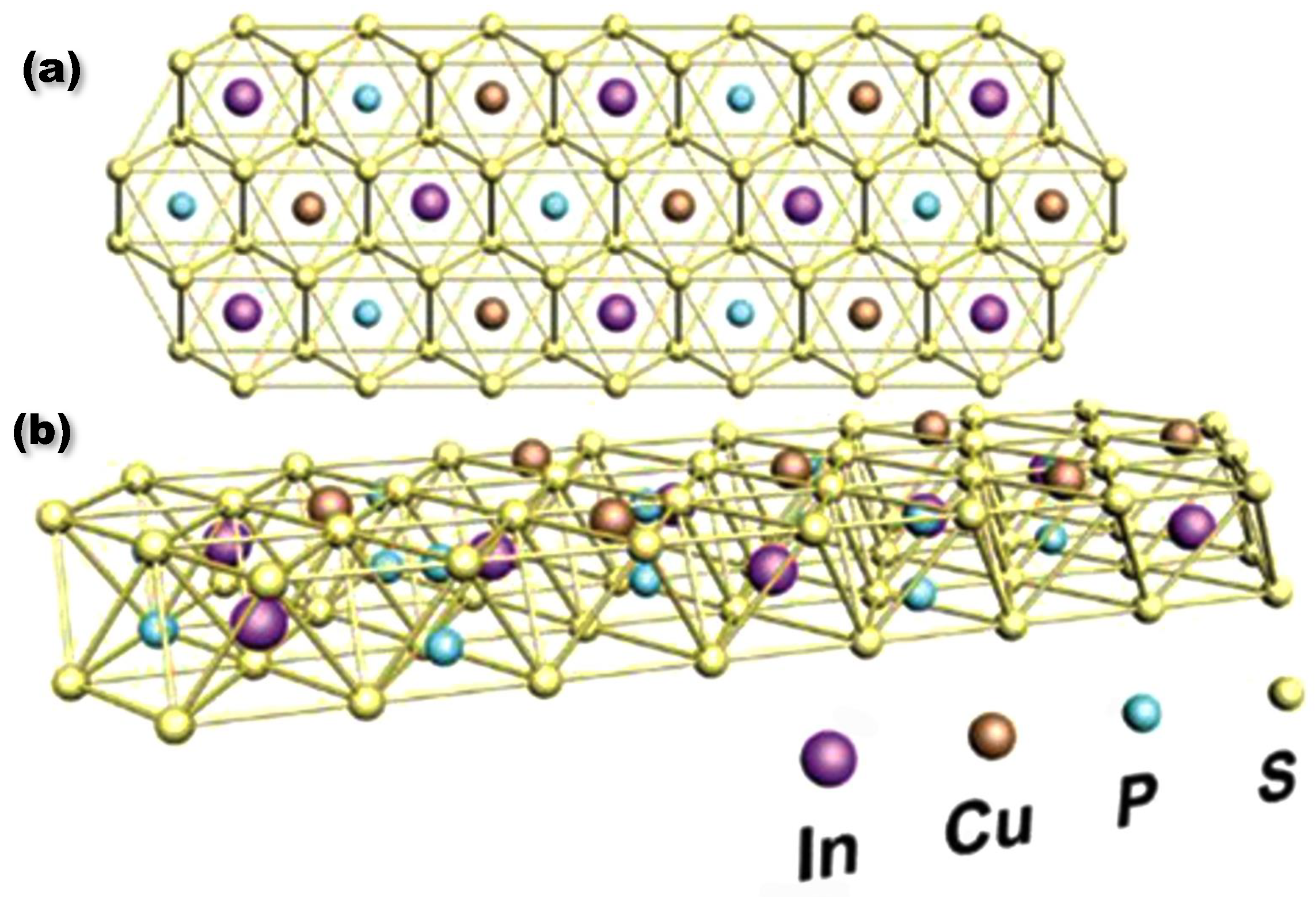
  10. Belianinov, A.; He, Q.; Dziaugys, A.; Maksymovych, P.; Eliseev, E.; Borisevich, A.; Morozovska, A.; Banys, J.; Vysochanskii, Y.; Kalinin, S.V. CuInP2S6 Room Temperature Layered Ferroelectric. Nano Lett. 2015, 15, 3808–3814. [Google Scholar] [CrossRef] [PubMed]
  11. Chang, K.; Liu, J.; Lin, H.; Wang, N.; Zhao, K.; Zhang, A.; Jin, F.; Zhong, Y.; Hu, X.; Duan, W.; et al. Discovery of robust in-plane ferroelectricity in atomic-thick SnTe. Science 2016, 353, 274–278. [Google Scholar] [CrossRef] [PubMed]
  12. Liu, F.; You, L.; Seyler, K.L.; Li, X.; Yu, P.; Lin, J.; Wang, X.; Zhou, J.; Wang, H.; He, H.; et al. Room-temperature ferroelectricity in CuInP2S6 ultrathin flakes. Nat. Commun. 2016, 7, 12357. [Google Scholar] [CrossRef] [PubMed]
  13. Xiao, J.; Zhu, H.; Wang, Y.; Feng, W.; Hu, Y.; Dasgupta, A.; Han, Y.; Wang, Y.; Muller, D.A.; Martin, L.W.; et al. Intrinsic Two-Dimensional Ferroelectricity with Dipole Locking. Phys. Rev. Lett. 2018, 120, 227601. [Google Scholar] [CrossRef] [PubMed]
  14. Varotto, S.; Nessi, L.; Cecchi, S.; Slawinska, J.; Noel, P.; Petrò, S.; Fagiani, F.; Novati, A.; Cantoni, M.; Petti, D.; et al. Room-temperature ferroelectric switching of spin-to-charge conversion in germanium telluride. Nat. Electron. 2021, 4, 740–747. [Google Scholar] [CrossRef]
  15. Andersen, T.I.; Scuri, G.; Sushko, A.; Greve, K.D.; Sung, J.; Zhou, Y.; Wild, D.S.; Gelly, R.J.; Heo, H.; Bérubé, D.; et al. Excitons in a reconstructed moiré potential in twisted WSe2/WSe2 homobilayers. Nat. Mater. 2021, 20, 480–487. [Google Scholar] [CrossRef]
  16. Son, S.; Lee, Y.; Kim, J.H.; Kim, B.H.; Kim, C.; Na, W.; Ju, H.; Park, S.; Nag, A.; Zhou, K.J.; et al. Multiferroic-Enabled Magnetic-Excitons in 2D Quantum-Entangled Van der Waals Antiferromagnet NiI2. Adv. Mater. 2021, 34, 2109144. [Google Scholar] [CrossRef]
  17. Song, Q.; Occhialini, C.A.; Ilyas, E.E.B.; Amoroso, D.; Barone, P.; Kapeghian, J.; Watanabe, K.; Taniguchi, T.; Botana, A.S.; Picozzi, S.; et al. Evidence for a single-layer van der Waals multiferroic. Nature 2022, 602, 601–605. [Google Scholar] [CrossRef]
  18. You, Y.M.; Liao, W.Q.; Zhao, D.; Ye, H.Y.; Zhang, Y.; Zhou, Q.; Niu, X.; Wang, J.; Li, P.F.; Fu, D.W.; et al. An organic-inorganic perovskite ferroelectric with large piezoelectric response. Science 2017, 357, 306–309. [Google Scholar] [CrossRef]
  19. Liu, Z.; Deng, L.; Peng, B. Ferromagnetic and ferroelectric two-dimensional materials for memory application. Adv. Mater. 2021, 14, 1802–1813. [Google Scholar] [CrossRef]
  20. Abdolhosseinzadeh, S.; Jiang, X.; Zhang, H.; Qiu, J.; Zhang, C.J. Perspectives on solution processing of two-dimensional MXenes. Mater. Today 2021, 48, 214–240. [Google Scholar] [CrossRef]
  21. Luo, Z.D.; Yang, M.M.; Liu, Y.; Alexe, M. Emerging Opportunities for 2D Semiconductor/Ferroelectric Transistor-Structure Devices. Adv. Mater. 2021, 33, 2005620. [Google Scholar] [CrossRef]
  22. Wang, J.; Hu, W. Recent progress on integrating two-dimensional materials with ferroelectrics for memory devices and photodetectors. Chin. Phys. B 2017, 26, 037106. [Google Scholar] [CrossRef]
  23. Mermin, N.D.; Wagner, H. Absence of Ferromagnetism or Antiferromagnetism in One- or Two-Dimensional Isotropic Heisenberg Models. Phys. Rev. Lett. 1966, 17, 1133–1136. [Google Scholar] [CrossRef]
  24. Liu, K.; Lu, J.; Picozzi, S.; Bellaiche, L.; Xiang, H. Intrinsic Origin of Enhancement of Ferroelectricity in SnTe Ultrathin Films. Phys. Rev. Lett. 2018, 121, 027601. [Google Scholar] [CrossRef]
  25. Zhang, J.; Song, X.; Wang, L.; Huang, W. Ultrathin two-dimensional hybrid perovskites toward flexible electronics and optoelectronics. Natl. Sci. Rev. 2021, 9, nwab129. [Google Scholar] [CrossRef]
  26. Lou, F.; Gu, T.; Ji, J.; Feng, J.; Xiang, H.; Stroppa, A. Tunable spin textures in polar antiferromagnetic hybrid organic–inorganic perovskites by electric and magnetic fields. npj Comput. Mater. 2020, 6, 114. [Google Scholar] [CrossRef]
  27. Kenzelmann, M.; Harris, A.B.; Jonas, S.; Broholm, C.; Schefer, J.; Kim, S.B.; Zhang, C.L.; Cheong, S.W.; Vajk, O.P.; Lynn, J.W. Magnetic Inversion Symmetry Breaking and Ferroelectricity in TbMnO3. Phys. Rev. Lett. 2005, 95, 087206. [Google Scholar] [CrossRef]
  28. Scott, J.F.; de Araujo, C.A.P. Ferroelectric Memories. Science 1989, 246, 1400–1405. [Google Scholar] [CrossRef]
  29. Moore, G.E. Cramming more components onto integrated circuits, Reprinted from Electronics, volume 38, number 8, April 19, 1965, pp.114 ff. IEEE Solid-State Circuits Soc. Newsl. 2006, 11, 33–35. [Google Scholar] [CrossRef]
  30. Waldrop, M.M. The chips are down for Moore’s law. Nature 2016, 530, 144–147. [Google Scholar] [CrossRef]
  31. Radamson, H.H.; Zhu, H.; Wu, Z.; He, X.; Lin, H.; Liu, J.; Xiang, J.; Kong, Z.; Xiong, W.; Li, J.; et al. State of the Art and Future Perspectives in Advanced CMOS Technology. Nanomaterials 2020, 10, 1555. [Google Scholar] [CrossRef]
  32. Nikonov, D.E.; Young, I.A. Benchmarking of Beyond-CMOS Exploratory Devices for Logic Integrated Circuits. IEEE J. Explor.-Solid-State Comput. Devices Circuits 2015, 1, 3–11. [Google Scholar] [CrossRef]
  33. International Roadmap for Devices and Systems, beyond CMOS and Emerging Materials Integration: 2022. Available online: https://irds.ieee.org/editions/2022/irds%E2%84%A2-2022-beyond-cmos-and-emerging-research-materials (accessed on 13 June 2023).
  34. Wang, Z.; Liu, X.; Zhou, X.; Yuan, Y.; Zhou, K.; Zhang, D.; Luo, H.; Sun, J. Reconfigurable Quasi-Nonvolatile Memory/Subthermionic FET Functions in Ferroelectric–2D Semiconductor vdW Architectures. Adv. Mater. 2022, 34, 2200032. [Google Scholar] [CrossRef]
  35. Müller, J.; Polakowski, P.; Mueller, S.; Mikolajick, T. Ferroelectric Hafnium Oxide Based Materials and Devices: Assessment of Current Status and Future Prospects. ECS J. Solid State Sci. Technol. 2015, 4, N30. [Google Scholar] [CrossRef]
  36. Böscke, T.S.; Müller, J.; Bräuhaus, D.; Schröder, U.; Böttger, U. Ferroelectricity in hafnium oxide: CMOS compatible ferroelectric field effect transistors. In Proceedings of the 2011 International Electron Devices Meeting, Washington, DC, USA, 5–7 December 2011; pp. 24.5.1–24.5.4. [Google Scholar] [CrossRef]
  37. Müller, J.; Böscke, T.S.; Müller, S.; Yurchuk, E.; Polakowski, P.; Paul, J.; Martin, D.; Schenk, T.; Khullar, K.; Kersch, A.; et al. Ferroelectric hafnium oxide: A CMOS-compatible and highly scalable approach to future ferroelectric memories. In Proceedings of the 2013 IEEE International Electron Devices Meeting, Washington, DC, USA, 9–11 December 2013; pp. 10.8.1–10.8.4. [Google Scholar] [CrossRef]
  38. Yurchuk, E.; Mueller, S.; Martin, D.; Slesazeck, S.; Schroeder, U.; Mikolajick, T.; Muller, J.; Paul, J.; Hoffmann, R.; Sundqvist, J.; et al. Origin of the endurance degradation in the novel HfO2-based 1T ferroelectric non-volatile memories. In Proceedings of the 2014 IEEE International Reliability Physics Symposium, Waikoloa, HI, USA, 1–5 June 2014; pp. 2E.5.1–2E.5.5. [Google Scholar]
  39. Tan, A.J.; Liao, Y.H.; Wang, L.C.; Shanker, N.; Bae, J.H.; Hu, C.; Salahuddin, S. Ferroelectric HfO2 Memory Transistors With High-k Interfacial Layer and Write Endurance Exceeding 1010 Cycles. IEEE Electron Device Lett. 2021, 42, 994–997. [Google Scholar] [CrossRef]
  40. Lemme, M.C.; Akinwande, D.; Huyghebaert, C.; Stampfer, C. 2D materials for future heterogeneous electronics. Nat. Commun. 2022, 13, 1392. [Google Scholar] [CrossRef]
  41. Ivanov, S.A.; Sarkar, T.; Fortalnova, E.A.; Politova, E.D.; Stefanovich, S.Y.; Safronenko, M.G.; Nordblad, P.; Mathieu, R. Composition dependence of the multifunctional properties of Nd-doped Bi4Ti3O12 ceramics. J. Mater. Sci. Mater. Electron. 2017, 28, 7692–7707. [Google Scholar] [CrossRef]
  42. Du, J.; Xie, D.; Zhang, Q.; Zhong, H.; Meng, F.; Fu, X.; Sun, Q.; Ni, H.; Li, T.; Guo, E.-j.; et al. A robust neuromorphic vision sensor with optical control of ferroelectric switching. Nano Energy 2021, 89, 106439. [Google Scholar] [CrossRef]
  43. Puebla, S.; Pucher, T.; Rouco, V.; Sanchez-Santolino, G.; Xie, Y.; Zamora, V.; Cuellar, F.A.; Mompean, F.J.; Leon, C.; Island, J.O.; et al. Combining Freestanding Ferroelectric Perovskite Oxides with Two-Dimensional Semiconductors for High Performance Transistors. Nano Lett. 2022, 22, 7457–7466. [Google Scholar] [CrossRef]
  44. Hiroyuki, Y.; Vincent, G.; Stéphane, F.; Sören, B.; Maya, M.; Alexandre, G.; Stéphane, X.; Julie, G.; Eric, J.; Cécile, C.; et al. Giant Electroresistance of Super-tetragonal BiFeO3-Based Ferroelectric Tunnel Junctions. ACS Nano 2013, 7, 5385–5390. [Google Scholar]
  45. Wang, J.; Neaton, J.B.; Zheng, H.; Nagarajan, V.; Ogale, S.B.; Liu, B.; Viehland, D.; Vaithyanathan, V.; Schlom, D.G.; Waghmare, U.V.; et al. Epitaxial BiFeO3 Multiferroic Thin Film Heterostructures. Science 2003, 299, 1719–1722. [Google Scholar] [CrossRef] [PubMed]
  46. Wang, N.; Luo, X.; Han, L.; Zhang, Z.; Zhang, R.; Olin, H.; Yang, Y. Structure, Performance, and Application of BiFeO3 Nanomaterials. Nano-Micro Lett. 2020, 12, 81. [Google Scholar] [CrossRef] [PubMed]
  47. Li, T.; Sharma, P.; Lipatov, A.; Lee, H.; Lee, J.W.; Zhuravlev, M.Y.; Paudel, T.R.; Genenko, Y.A.; Eom, C.B.; Tsymbal, E.Y.; et al. Polarization-Mediated Modulation of Electronic and Transport Properties of Hybrid MoS2–BaTiO3–SrRuO3 Tunnel Junctions. Nano Lett. 2017, 17, 922–927. [Google Scholar] [CrossRef]
  48. Fei, Z.; Zhao, W.; Palomaki, T.A.; Sun, B.; Miller, M.K.; Zhao, Z.; Yan, J.; Xu, X.; Cobden, D.H. Ferroelectric switching of a two-dimensional metal. Nature 2018, 560, 336–339. [Google Scholar] [CrossRef]
  49. Shuoguo, Y.; Xin, L.; Lit, C.H.; Chengcheng, X.; Yawei, D.; Maohai, X.; Jianhua, H. Room-temperature ferroelectricity in MoTe2 down to the atomic monolayer limit. Nat. Commun. 2019, 10, 1775. [Google Scholar] [CrossRef]
  50. Lu, Y.; Fucai, L.; Hongsen, L.; Hu, Y.; Shuang, Z.; Lei, C.; Yang, Z.; Qundong, F.; Guoliang, Y.; Shuai, D.; et al. In-Plane Ferroelectricity in Thin Flakes of Van der Waals Hybrid Perovskite. Adv. Mater. 2018, 30, 1803249. [Google Scholar] [CrossRef]
  51. Zheng, C.; Yu, L.; Zhu, L.; Collins, J.L.; Kim, D.; Lou, Y.; Xu, C.; Li, M.; Wei, Z.; Zhang, Y.; et al. Room temperature in-plane ferroelectricity in van der Waals In2Se3. Sci. Adv. 2018, 4, eaar7720. [Google Scholar] [CrossRef]
  52. Wang, H.; Lu, W.; Hou, S.; Yu, B.; Zhou, Z.; Xue, Y.; Guo, R.; Wang, S.; Zeng, K.; Yan, X. A 2D-SnSe film with ferroelectricity and its bio-realistic synapse application. Nanoscale 2020, 12, 21913–21922. [Google Scholar] [CrossRef]
  53. Kwon, K.C.; Zhang, Y.; Wang, L.; Yu, W.; Wang, X.; Park, I.H.; Choi, H.S.; Ma, T.; Zhu, Z.; Tian, B.; et al. In-Plane Ferroelectric Tin Monosulfide and Its Application in a Ferroelectric Analog Synaptic Device. ACS Nano 2020, 14, 7628–7638. [Google Scholar] [CrossRef]
  54. Hu, Z.; Li, Q.; Li, M.; Wang, Q.; Zhu, Y.; Liu, X.; Zhao, X.; Liu, Y.; Dong, S. Ferroelectric memristor based on Pt/BiFeO3/Nb-doped SrTiO3 heterostructure. Appl. Phys. Lett. 2013, 102, 102901. [Google Scholar] [CrossRef]
  55. Kim, S.; Heo, K.; Lee, S.; Seo, S.; Kim, H.; Cho, J.; Lee, H.; Lee, K.B.; Park, J.H. Ferroelectric polymer-based artificial synapse for neuromorphic computing. Nanoscale Horiz. 2021, 6, 139–147. [Google Scholar] [CrossRef]
  56. Chen, L.; Pam, M.E.; Li, S.; Ang, K.W. Ferroelectric memory based on two-dimensional materials for neuromorphic computing. Neuromorphic Comput. Eng. 2022, 2, 022001. [Google Scholar] [CrossRef]
  57. Tian, B.; Liu, L.; Yan, M.; Wang, J.; Zhao, Q.; Zhong, N.; Xiang, P.; Sun, L.; Peng, H.; Shen, H.; et al. A Robust Artificial Synapse Based on Organic Ferroelectric Polymer. Adv. Electron. Mater. 2019, 5, 1800600. [Google Scholar] [CrossRef]
  58. Chen, Y.H.; Cheng, C.Y.; Chen, S.Y.; Rodriguez, J.S.D.; Liao, H.T.; Watanabe, K.; Taniguchi, T.; Chen, C.W.; Sankar, R.; Chou, F.C.; et al. Oxidized-monolayer tunneling barrier for strong Fermi-level depinning in layered InSe transistors. npj 2D Mater. Appl. 2019, 3, 49. [Google Scholar] [CrossRef]
  59. Wang, L.; Wang, X.; Zhang, Y.; Li, R.; Ma, T.; Leng, K.; Chen, Z.; Abdelwahab, I.; Loh, K.P. Exploring Ferroelectric Switching in α-In2Se3 for Neuromorphic Computing. Adv. Funct. Mater. 2020, 30, 2004609. [Google Scholar] [CrossRef]
  60. Ding, W.; Zhu, J.; Wang, Z.; Gao, Y.; Xiao, D.; Gu, Y.; Zhang, Z.; Zhu, W. Prediction of intrinsic two-dimensional ferroelectrics in In2Se3 and other III2-VI3 van der Waals materials. Nat. Commun. 2017, 8, 14956. [Google Scholar] [CrossRef]
  61. Yu, Z.; Wu, D.; Zhu, Y.; Cho, Y.; He, Q.; Yang, X.; Herrera, K.; Chu, Z.; Han, Y.; Downer, M.C.; et al. Out-of-Plane Piezoelectricity and Ferroelectricity in Layered α-In2Se3 Nanoflakes. Nano Lett. 2017, 17, 5508–5513. [Google Scholar] [CrossRef]
  62. Xue, F.; He, X.; Retamal, J.R.D.; Han, A.; Zhang, J.; Liu, Z.; Huang, J.K.; Hu, W.; Tung, V.; He, J.H.; et al. Gate-Tunable and Multidirection-Switchable Memristive Phenomena in a Van Der Waals Ferroelectric. Adv. Mater. 2019, 31, 1901300. [Google Scholar] [CrossRef]
  63. Si, M.; Saha, A.K.; Gao, S.; Qiu, G.; Qin, J.; Duan, Y.; Jian, J.; Niu, C.; Wang, H.; Wu, W.; et al. A ferroelectric semiconductor field-effect transistor. Nat. Electron. 2019, 2, 580–586. [Google Scholar] [CrossRef]
  64. Island, J.O.; Blanter, S.I.; Buscema, M.; van der Zant, H.S.J.; Castellanos-Gomez, A. Gate Controlled Photocurrent Generation Mechanisms in High-Gain In2Se3 Phototransistors. Nano Lett. 2015, 15, 7853–7858. [Google Scholar] [CrossRef]
  65. Yang, J.Y.; Yeom, M.J.; Park, Y.; Heo, J.; Yoo, G. Ferroelectric α-In2Se3 Wrapped-Gate β-Ga2O3 Field-Effect Transistors for Dynamic Threshold Voltage Control. Adv. Electron. Mater. 2021, 7, 2100306. [Google Scholar] [CrossRef]
  66. Liu, X.; Wu, G.; Zeng, J.; Bai, C.; Li, W.; Wang, J.; Chu, J. Two-dimensional α-In2Se3-based ferroelectric semiconductor junction for reconfigurable photodetectors. Appl. Phys. Lett. 2023, 122, 193101. [Google Scholar] [CrossRef]
  67. Li, B.; Li, S.; Wang, H.; Chen, L.; Liu, L.; Feng, X.; Li, Y.; Chen, J.; Gong, X.; Ang, K.W. An Electronic Synapse Based on 2D Ferroelectric CuInP2S6. Adv. Electron. Mater. 2020, 6, 2000760. [Google Scholar] [CrossRef]
  68. Li, X.; Chen, X.; Deng, W.; Li, S.; An, B.; Chu, F.; Wu, Y.; Liu, F.; Zhang, Y. An all-two-dimensional Fe-FET retinomorphic sensor based on the novel gate dielectric In2Se3−xOx. Nanoscale 2023, 15, 10705–10714. [Google Scholar] [CrossRef]
  69. Das, S.; Sebastian, A.; Pop, E.; McClellan, C.J.; Franklin, A.D.; Grasser, T.; Knobloch, T.; Illarionov, Y.; Penumatcha, A.V.; Appenzeller, J.; et al. Transistors based on two-dimensional materials for future integrated circuits. Nat. Electron. 2021, 4, 786–799. [Google Scholar] [CrossRef]
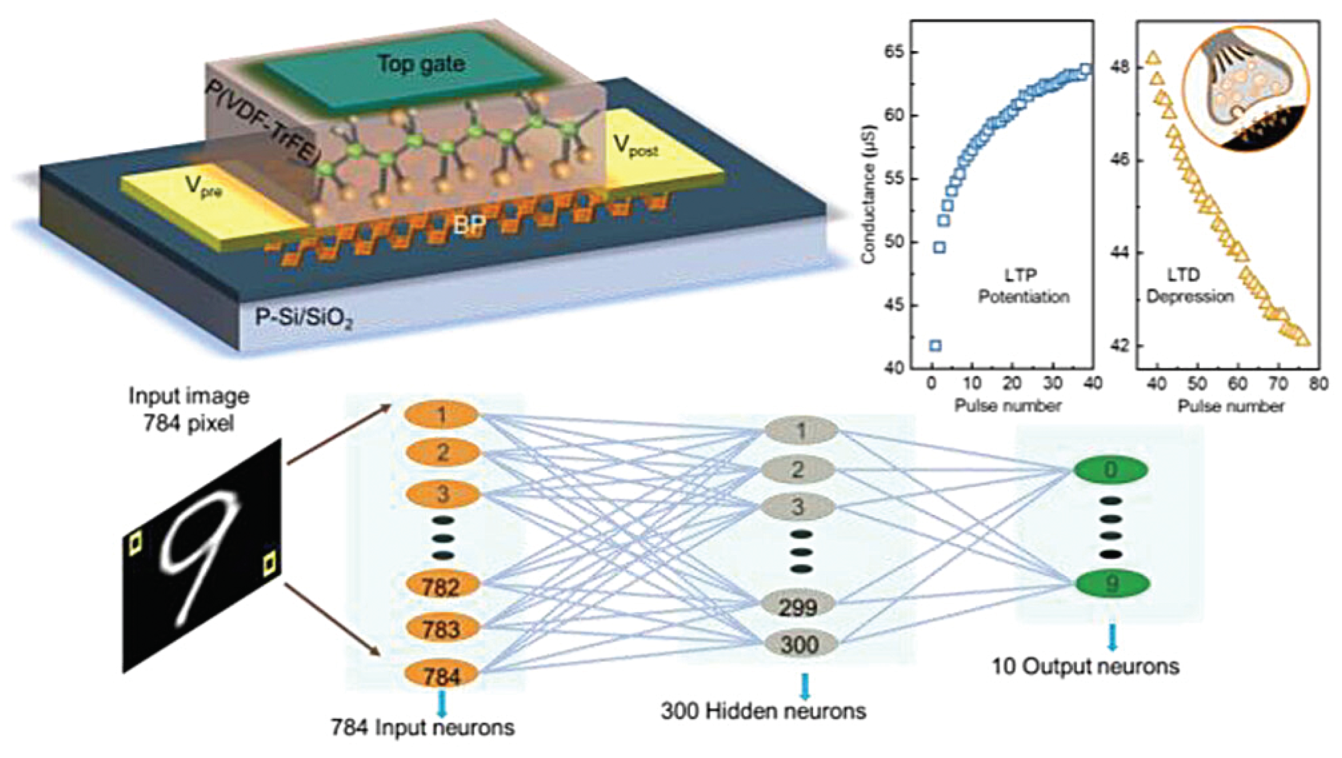
  70. Dang, Z.; Guo, F.; Duan, H.; Zhao, Q.; Fu, Y.; Jie, W.; Jin, K.; Hao, J. Black Phosphorus/Ferroelectric P(VDF-TrFE) Field-Effect Transistors with High Mobility for Energy-Efficient Artificial Synapse in High-Accuracy Neuromorphic Computing. Nano Lett. 2023, 23, 6752–6759. [Google Scholar] [CrossRef]
  71. Dang, Z.; Guo, F.; Wu, Z.; Jin, K.; Hao, J. Interface Engineering and Device Applications of 2D Ultrathin Film/Ferroelectric Copolymer P(VDF-TrFE). Adv. Phys. Res. 2023, 2, 2200038. [Google Scholar] [CrossRef]
  72. Kim, S.; Dong, Y.; Hossain, M.M.; Gorman, S.; Towfeeq, I.; Gajula, D.; Childress, A.; Rao, A.M.; Koley, G. Piezoresistive Graphene/P(VDF-TrFE) Heterostructure Based Highly Sensitive and Flexible Pressure Sensor. ACS Appl. Mater. Interfaces 2019, 11, 16006–16017. [Google Scholar] [CrossRef]
  73. Li, E.; Wu, X.; Chen, Q.; Wu, S.; He, L.; Yu, R.; Hu, Y.; Chen, H.; Guo, T. Nanoscale channel organic ferroelectric synaptic transistor array for high recognition accuracy neuromorphic computing. Nano Energy 2021, 85, 106010. [Google Scholar] [CrossRef]
  74. Jin, L.; Wang, H.; Cao, R.; Khan, K.; Tareen, A.K.; Wageh, S.; Al-Ghamdi, A.A.; Li, S.; Li, D.; Zhang, Y.; et al. The rise of 2D materials/ferroelectrics for next generation photonics and optoelectronics devices. APL Mater. 2022, 10, 060903. [Google Scholar] [CrossRef]
  75. Qiu, D.Y.; da Jornada, F.H.; Louie, S.G. Optical Spectrum of MoS2: Many-Body Effects and Diversity of Exciton States. Phys. Rev. Lett. 2013, 111, 216805. [Google Scholar] [CrossRef]
  76. He, K.; Kumar, N.; Zhao, L.; Wang, Z.; Mak, K.F.; Zhao, H.; Shan, J. Tightly Bound Excitons in Monolayer WSe2. Phys. Rev. Lett. 2014, 113, 026803. [Google Scholar] [CrossRef]
  77. Xia, F.; Wang, H.; Xiao, D.; Dubey, M.; Ramasubramaniam, A. Two-dimensional material nanophotonics. Nat. Photonics 2014, 8, 899–907. [Google Scholar] [CrossRef]
  78. Wang, X.; Cui, Y.; Li, T.; Lei, M.; Li, J.; Wei, Z. Recent Advances in the Functional 2D Photonic and Optoelectronic Devices. Adv. Opt. Mater. 2019, 7, 1801274. [Google Scholar] [CrossRef]
  79. Mak, K.F.; Shan, J. Photonics and optoelectronics of 2D semiconductor transition metal dichalcogenides. Nat. Photonics 2016, 10, 216–226. [Google Scholar] [CrossRef]
  80. Qiu, Q.; Huang, Z. Photodetectors of 2D Materials from Ultraviolet to Terahertz Waves. Adv. Mater. 2021, 33, 2008126. [Google Scholar] [CrossRef]
  81. Fu, J.; Qiu, M.; Bao, W.; Zhang, H. Frontiers in Electronic and Optoelectronic Devices Based on 2D Materials. Adv. Electron. Mater. 2021, 7, 2100444. [Google Scholar] [CrossRef]
  82. Guan, H.; Hong, J.; Wang, X.; Ming, J.; Zhang, Z.; Liang, A.; Han, X.; Dong, J.; Qiu, W.; Chen, Z.; et al. Broadband, High-Sensitivity Graphene Photodetector Based on Ferroelectric Polarization of Lithium Niobate. Adv. Opt. Mater. 2021, 9, 2100245. [Google Scholar] [CrossRef]
  83. Sun, Y.; Niu, G.; Ren, W.; Meng, X.; Zhao, J.; Luo, W.; Ye, Z.G.; Xie, Y.H. Hybrid System Combining Two-Dimensional Materials and Ferroelectrics and Its Application in Photodetection. ACS Nano 2021, 15, 10982–11013. [Google Scholar] [CrossRef]
  84. Guo, J.; Liu, Y.; Lin, Y.; Tian, Y.; Zhang, J.; Gong, T.; Cheng, T.; Huang, W.; Zhang, X. Simulation of tuning graphene plasmonic behaviors by ferroelectric domains for self-driven infrared photodetector applications. Nanoscale 2019, 11, 20868–20875. [Google Scholar] [CrossRef]
  85. Wang, H.; Zhao, H.; Hu, G.; Li, S.; Su, H.; Zhang, J. Graphene Based Surface Plasmon Polariton Modulator Controlled by Ferroelectric Domains in Lithium Niobate. Sci. Rep. 2015, 5, 18258. [Google Scholar] [CrossRef]
  86. Lee, Y.T.; Hwang, D.K.; Choi, W.K. High-performance black phosphorus top-gate ferroelectric transistor for nonvolatile memory applications. J. Korean Phys. Soc. 2016, 69, 1347–1351. [Google Scholar] [CrossRef]
  87. Xie, L.; Chen, X.; Dong, Z.; Yu, Q.; Zhao, X.; Yuan, G.; Zeng, Z.; Wang, Y.; Zhang, K. Nonvolatile Photoelectric Memory Induced by Interfacial Charge at a Ferroelectric PZT-Gated Black Phosphorus Transistor. Adv. Electron. Mater. 2019, 5, 1900458. [Google Scholar] [CrossRef]
  88. Yan, J.M.; Ying, J.S.; Yan, M.Y.; Wang, Z.C.; Li, S.S.; Chen, T.W.; Gao, G.Y.; Liao, F.; Luo, H.S.; Zhang, T.; et al. Optoelectronic Coincidence Detection with Two-Dimensional Bi2O2Se Ferroelectric Field-Effect Transistors. Adv. Funct. Mater. 2021, 31, 2103982. [Google Scholar] [CrossRef]
  89. Zhang, X.; Huang, H.; Yao, X.; Li, Z.; Zhou, C.; Zhang, X.; Chen, P.; Fu, L.; Zhou, X.; Wang, J.; et al. Ultrasensitive Mid-wavelength Infrared Photodetection Based on a Single InAs Nanowire. ACS Nano 2019, 13, 3492–3499. [Google Scholar] [CrossRef]
  90. Wang, X.; Wang, P.; Wang, J.; Hu, W.; Zhou, X.; Guo, N.; Huang, H.; Sun, S.; Shen, H.; Lin, T.; et al. Ultrasensitive and Broadband MoS2 Photodetector Driven by Ferroelectrics. Adv Mater. 2015, 27, 6575–6581. [Google Scholar] [CrossRef] [PubMed]
  91. Liu, L.; Wu, L.; Wang, A.; Liu, H.; Ma, R.; Wu, K.; Chen, J.; Zhou, Z.; Tian, Y.; Yang, H.; et al. Ferroelectric-Gated InSe Photodetectors with High On/Off Ratios and Photoresponsivity. Nano Lett. 2020, 20, 6666–6673. [Google Scholar] [CrossRef] [PubMed]
  92. Wu, M. Two-Dimensional van der Waals Ferroelectrics: Scientific and Technological Opportunities. ACS Nano 2021, 15, 9229–9237. [Google Scholar] [CrossRef]
  93. Li, P.; Chaturvedi, A.; Zhou, H.; Zhang, G.; Li, Q.; Xue, J.; Zhou, Z.; Wang, S.; Zhou, K.; Weng, Y.; et al. Electrostatic Coupling in MoS2/CuInP2S6 Ferroelectric vdW Heterostructures. Adv. Funct. Mater. 2022, 32, 2201359. [Google Scholar] [CrossRef]
  94. Hill, N.A. Why Are There so Few Magnetic Ferroelectrics? J. Phys. Chem. B 2000, 104, 6694–6709. [Google Scholar] [CrossRef]
  95. Eerenstein, W.; Mathur, N.D.; Scott, J.F. Multiferroic and magnetoelectric materials. Nature 2006, 442, 759–765. [Google Scholar] [CrossRef]
  96. Ramesh, R.; Spaldin, N.A. Multiferroics: Progress and prospects in thin films. Nat. Mater. 2007, 6, 21–29. [Google Scholar] [CrossRef]
  97. Beckman, S.P.; Wang, X.; Rabe, K.M.; Vanderbilt, D. Ideal barriers to polarization reversal and domain-wall motion in strained ferroelectric thin films. Phys. Rev. B 2009, 79, 144124. [Google Scholar] [CrossRef]
  98. Khitun, A.; Wang, K.L. Non-volatile magnonic logic circuits engineering. J. Appl. Phys. 2011, 110, 034306. [Google Scholar] [CrossRef]
  99. Manipatruni, S.; Nikonov, D.E.; Lin, C.C.; Gosavi, T.A.; Liu, H.; Prasad, B.; Huang, Y.L.; Bonturim, E.; Ramesh, R.; Young, I.A. Scalable energy-efficient magnetoelectric spin–orbit logic. Nature 2019, 565, 35–42. [Google Scholar] [CrossRef] [PubMed]
  100. Kuzmenko, A.M.; Szaller, D.; Kain, T.; Dziom, V.; Weymann, L.; Shuvaev, A.; Pimenov, A.; Mukhin, A.A.; Ivanov, V.Y.; Gudim, I.A.; et al. Switching of Magnons by Electric and Magnetic Fields in Multiferroic Borates. Phys. Rev. Lett. 2018, 120, 027203. [Google Scholar] [CrossRef] [PubMed]
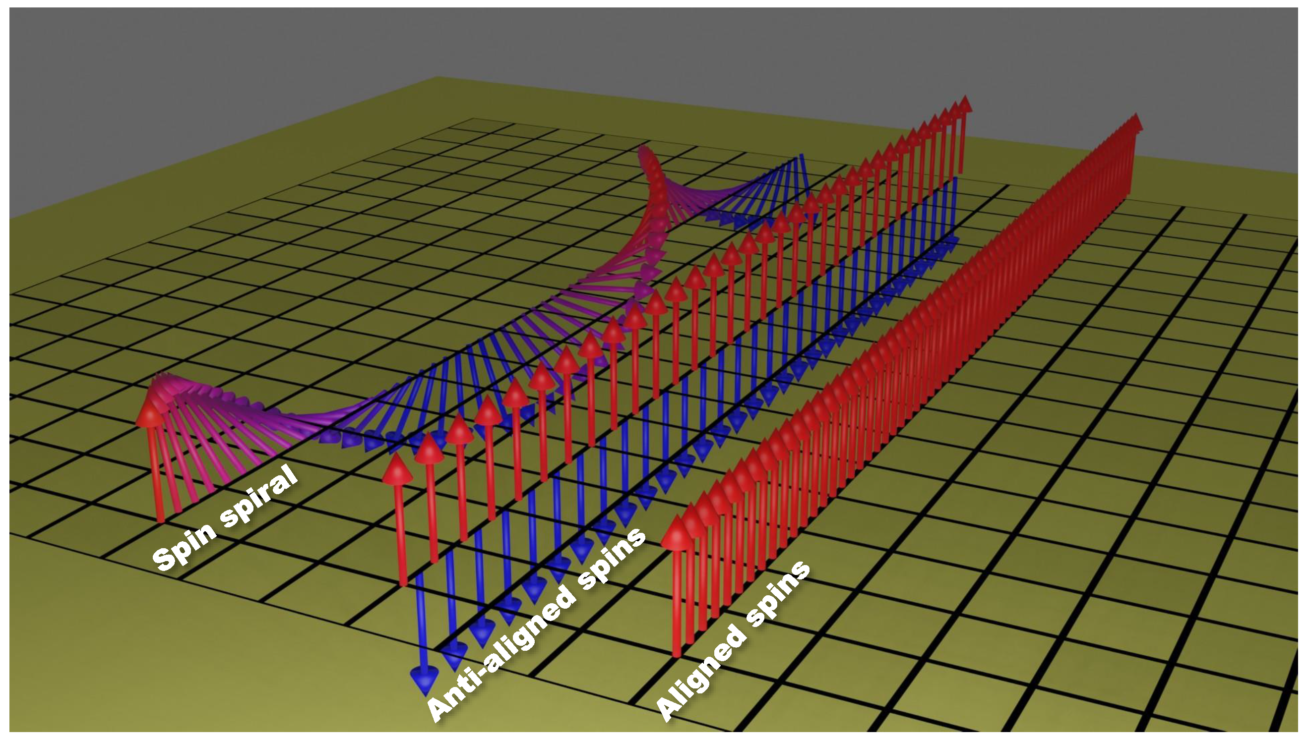
  101. Mai, T.T.; Garrity, K.F.; McCreary, A.; Argo, J.; Simpson, J.R.; Doan-Nguyen, V.; Aguilar, R.V.; Walker, A.R.H. Magnon-phonon hybridization in 2D antiferromagnet MnPSe3. Sci. Adv. 2021, 7, eabj3106. [Google Scholar] [CrossRef]
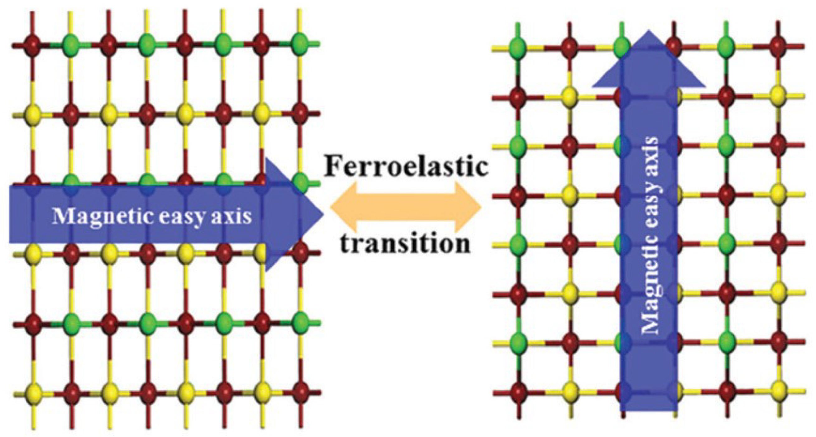
  102. Wang, X.; Shang, Z.; Zhang, C.; Kang, J.; Liu, T.; Wang, X.; Chen, S.; Liu, H.; Tang, W.; Zeng, Y.J.; et al. Electrical and magnetic anisotropies in van der Waals multiferroic CuCrP2S6. Nat. Commun. 2023, 14, 840. [Google Scholar] [CrossRef]
  103. Xu, B.; Li, S.; Jiang, K.; Yin, J.; Liu, Z.; Cheng, Y.; Zhong, W. Switching of the magnetic anisotropy via strain in two dimensional multiferroic materials: CrSX (X = Cl, Br, I). Appl. Phys. Lett. 2020, 116, 052403. [Google Scholar] [CrossRef]
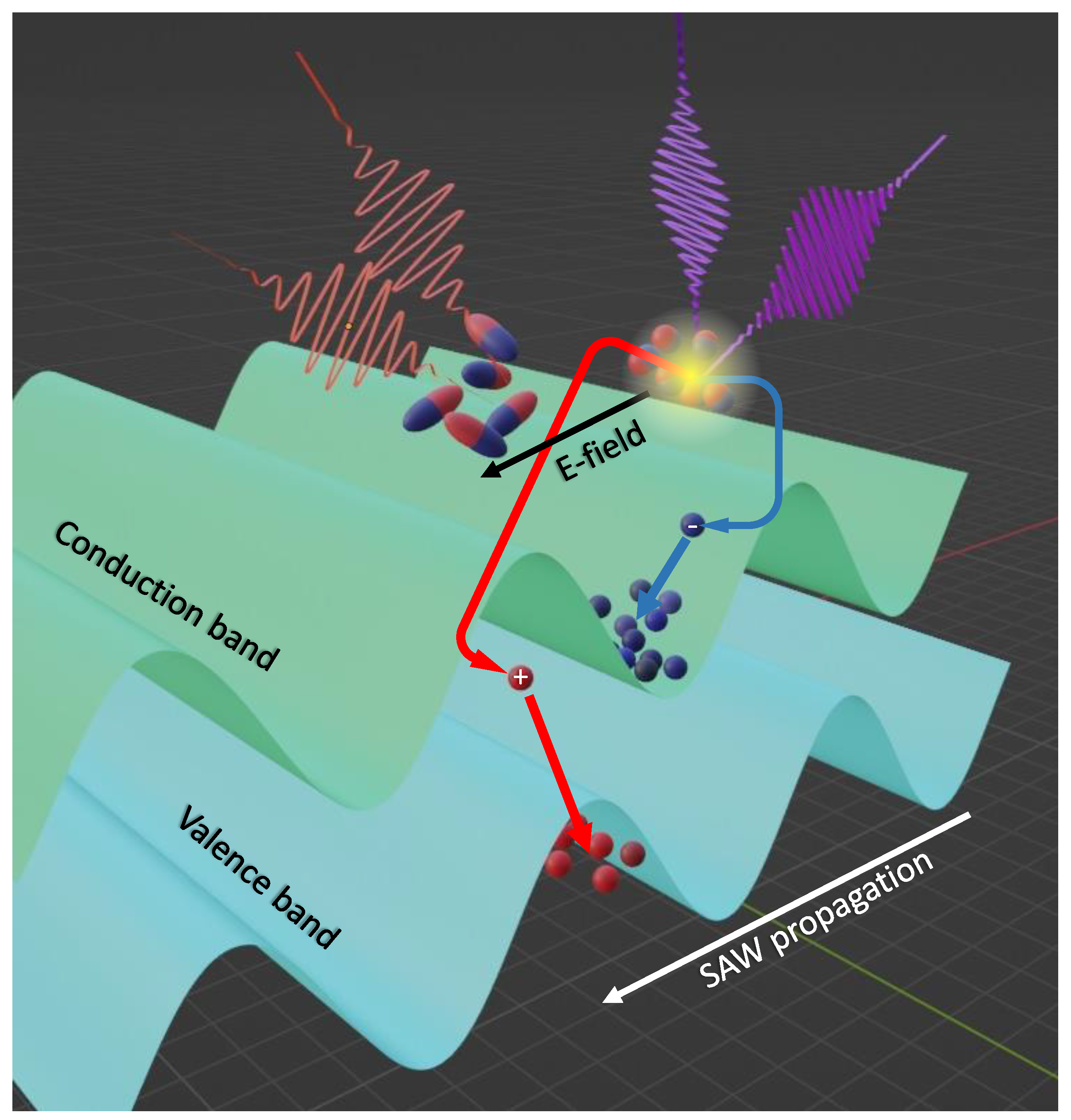
  104. Balandin, A.A.; Nika, D.L. Phononics in low-dimensional materials. Mater. Today 2012, 15, 266–275. [Google Scholar] [CrossRef]
  105. Delsing, P.; Cleland, A.N.; Schuetz, M.J.A.; Knörzer, J.; Giedke, G.; Cirac, J.I.; Srinivasan, K.; Wu, M.; Balram, K.C.; Bäuerle, C.; et al. The 2019 surface acoustic waves roadmap. J. Phys. D Appl. Phys. 2019, 52, 353001. [Google Scholar] [CrossRef]
  106. Wang, J.Q.; Zhang, Z.D.; Yu, S.Y.; Ge, H.; Liu, K.F.; Wu, T.; Sun, X.C.; Liu, L.; Chen, H.Y.; He, C.; et al. Extended topological valley-locked surface acoustic waves. Nat. Commun. 2022, 13, 1324. [Google Scholar] [CrossRef]
  107. Sukhachov, P.O.; Rostami, H. Acoustogalvanic Effect in Dirac and Weyl Semimetals. Phys. Rev. Lett. 2020, 124, 126602. [Google Scholar] [CrossRef] [PubMed]
  108. Sonowal, K.; Boev, D.V.; Kalameitsev, A.V.; Kovalev, V.M.; Savenko, I.G. Valley spin-acoustic resonance in MoS2 monolayers. Phys. Rev. B 2022, 106, 155426. [Google Scholar] [CrossRef]
  109. Kawada, T.; Kawaguchi, M.; Funato, T.; Kohno, H.; Hayashi, M. Acoustic spin Hall effect in strong spin-orbit metals. Sci. Adv. 2021, 7, eabd9697. [Google Scholar] [CrossRef] [PubMed]
  110. Zheng, S.; Wu, E.; Feng, Z.; Zhang, R.; Xie, Y.; Yu, Y.; Zhang, R.; Li, Q.; Liu, J.; Pang, W.; et al. Acoustically enhanced photodetection by a black phosphorus–MoS2 van der Waals heterojunction p–n diode. Nanoscale 2018, 10, 10148–10153. [Google Scholar] [CrossRef]
  111. Datta, K.; Li, Z.; Lyu, Z.; Deotare, P.B. Piezoelectric Modulation of Excitonic Properties in Monolayer WSe2 under Strong Dielectric Screening. ACS Nano 2021, 15, 12334–12341. [Google Scholar] [CrossRef] [PubMed]
  112. Jin, X.; O’Hara, A.; Zhang, Y.Y.; Du, S.; Pantelides, S.T. Designing strong and tunable magnetoelectric coupling in 2D trilayer heterostructures. 2D Mater. 2022, 10, 015007. [Google Scholar] [CrossRef]
  113. Zhang, M.; Guo, H.M.; Lv, J.; Wu, H.S. Electronic and magnetic properties of 5d transition metal substitution doping monolayer antimonene: Within GGA and GGA + U framework. Appl. Surf. Sci. 2020, 508, 145197. [Google Scholar] [CrossRef]
  114. Zhang, J.J.; Zhu, D.; Yakobson, B.I. Heterobilayer with Ferroelectric Switching of Topological State. Nano Lett. 2021, 21, 785–790. [Google Scholar] [CrossRef]
  115. Vitale, S.A. Valleytronics in 2D Materials. In Beyond-CMOS; John Wiley & Sons, Ltd.: Hoboken, NJ, USA, 2023; Chapter 6; pp. 209–250. [Google Scholar] [CrossRef]
  116. Ke, C.; Huang, J.; Liu, S. Two-dimensional ferroelectric metal for electrocatalysis. Mater. Horiz. 2021, 8, 3387–3393. [Google Scholar] [CrossRef]
Figure 1. Schematic representation of the main devices and 2D ferroelectric materials currently studied.
Solids 05 00004 g001
Figure 2. Panel(A) shows the electric current and polarization changes when different voltages are applied to TMCM-MnCl 3 , which is composed of molecules arranged in layers. Panel (B) shows the changes of the real part of the dielectric permittivity for different temperatures and frequencies. Panel (C) shows the piezoelectric coefficient as a function of temperature, demonstrating the ability to convert electric energy into mechanical energy, and vice versa. In panel (D), a comparison of the piezoelectric coefficient is shown between TMCM-MnCl 3 and other materials performed under the same experimental conditions, both organic and inorganic. Reprinted with permission from ref. [18].
Solids 05 00004 g002
Figure 3. Device with a thin layer of MoS 2 , as a channel, and a thin layer of ferroelectric Bi 4 Ti 3 O 1 2 (BiT)BiT, a material that can switch its electric polarization. How these two layers are connected in (a,b) is shown. The oxygen atoms that are missing from the BiT layer affect the device performance in (c). Three different regions are shown: (I) oxygen vacancies can capture or release electrons from the MoS 2 layer, changing its conductivity. (II) The oxygen vacancies can move around in the BiT layer when we apply an electric field, changing its polarization. (III) The oxygen vacancies can interact with the boundaries between different regions of polarization in the BiT layer, changing its stability. Reprinted with permission from [34].
Solids 05 00004 g003
Figure 4. Schematic representation of the device structure with (a) three terminals and (b) two terminals.
Solids 05 00004 g004
Figure 5. Metal layer (Pt), a layer that can change its electric polarization (ferroelectric), and a layer that can change its resistance (NSTO), can store information in two different states. In (a,b), it is shown how the electric charges are arranged in the device when it is in the low-resistance state and the high-resistance state, respectively. In (c,d), the energy levels of the different layers change when the device switches from low to high resistance are proposed. Reprinted with permission from ref. [54].
Solids 05 00004 g005
Figure 6. The device uses three thin layers of different materials: the top layer is single-layer graphene (SLG), the middle layer is a-In 2 Se 3 , the bottom layer is few-layer graphene (FLG). In (a,b), the device is shown. In (c,d), the thickness and the structure of each layer are measured via scanning with a tiny probe. In (e,f), the a-In 2 Se 3 layer shows the property of changing the polarization. Reprinted with permission from ref. [66].
Solids 05 00004 g006
Figure 7. The atom arrangement in CCPS, a material made of copper, chromium, phosphorus, and sulfur. In (a) we can see how the different layers of atoms are stacked on top of each other. In (b), we can see how the atoms are distributed within each layer. The colors used to represent the atoms are as follows: green for copper, blue for chromium, red for phosphorus, and yellow for sulfur. Reprinted with permission from ref. [67].
Solids 05 00004 g007
Figure 8. A device using two organic materials, copolymer poly(vinylidene fluoride-trifluoroethylene) P(VDF-TrFE) and black phosphorus (BP), to create a memory element that can store information by switching its electric polarization, is shown. P(VDF-TrFE) is a polymer that can change its polarization by applying an electric field, and BP is a thin layer that can conduct electricity. Reprinted with permission from ref. [70].
Solids 05 00004 g008
Figure 9. Representation of how magnetic anisotropy is switched by ferroelastic strain in CrSBr, CrSI, and CrSCl monolayers. Reprinted with permission from ref. [103].
Solids 05 00004 g009
Figure 10. Schematic representation of the spin-wave state, anti-aligned state, and spin-polarized state.
Solids 05 00004 g010
Figure 11. Schematic overview of surface acoustic waves; details in the main text.
Solids 05 00004 g011
Disclaimer/Publisher’s Note: The statements, opinions and data contained in all publications are solely those of the individual author(s) and contributor(s) and not of MDPI and/or the editor(s). MDPI and/or the editor(s) disclaim responsibility for any injury to people or property resulting from any ideas, methods, instructions or products referred to in the content.

