Article

A Comparative Study of n- and p-Channel FeFETs with Ferroelectric HZO Gate Dielectric

1
Electrical & Microelectronic Engineering, Rochester Institute of Technology, New York, NY 14623, USA
2
Department of Electronic Science, University of Delhi South Campus, New Delhi 110021, India
3
Department of Electronics & Communication Engineering, Faculty of Technology, University of Delhi, New Delhi 110007, India
4
Department of Electronics, Deen Dayal Upadhyaya College, University of Delhi, New Delhi 110078, India
5
Micron Technology Inc., Manassas, VA 20110, USA
*
Author to whom correspondence should be addressed.
Solids 2023, 4(4), 356-367; https://doi.org/10.3390/solids4040023
Submission received: 30 September 2023 / Revised: 18 November 2023 / Accepted: 23 November 2023 / Published: 1 December 2023
(This article belongs to the Special Issue Recent Advance in Ferroelectric Composites)

Abstract

:
This study investigates the electrical characteristics observed in n-channel and p-channel ferroelectric field effect transistor (FeFET) devices fabricated through a similar process flow with 10 nm of ferroelectric hafnium zirconium oxide (HZO) as the gate dielectric. The n-FeFETs demonstrate a faster complete polarization switching compared to the p-channel counterparts. Detailed and systematic investigations using TCAD simulations reveal the role of fixed charges and interface traps at the HZO-interfacial layer (HZO/IL) interface in modulating the subthreshold characteristics of the devices. A characteristic crossover point observed in the transfer characteristics of n-channel devices is attributed with the temporary switching between ferroelectric-based operation to charge-based operation, caused by the pinning effect due to the presence of different traps. This experimental study helps understand the role of charge trapping effects in switching characteristics of n- and p-channel ferroelectric FETs.

1. Introduction

Ferroelectric field effect transistors (FeFETs), particularly hafnium oxide (HfO2) based FeFETs, have captured the interest of semiconductor technology as the dominant candidates for future memory applications. FeFETs have all the design components of a traditional MOSFET with a sandwiched ferroelectric material layer as the gate dielectric. The two polarization states of the dielectric determine two separate threshold voltages giving rise to a memory window (MW) between two non-volatile memory states.
The discovery of ferroelectricity in hafnium oxide based dielectrics that are CMOS compatible has attracted enormous interests in integrating FeFETs in emerging non volatile memory, in-memory computing, and neuromorphic computing applications [1,2,3]. Apart from these, FeFETs also find applications in the domain of flexible electronics [4], particularly using structured memory arrays which can be used to mimic important biological functions for brain—inspired computing, or to emulate artificial synaptic responses for neuromorphic computing as discussed above [5]. This is in conjunction with rapid developments in artificial intelligence (AI) technology, which has put forward the requirements for high-speed, energy efficient, and non-volatile memories [6,7,8]. In this regard, the research community has observed a shift from the existing von Neumann computer architectures, driven by developments in FeFET technology [9,10,11]. FeFETs have demonstrated scalability, low power operation due to their CMOS compatibility, and faster non-destructible read/write operation capabilities.
The ferroelectricity observed in ferroelectric materials is primarily due to their non-centrosymmetric structure [1]. A large number of ferroelectric materials have been reported in the literature, however the most popular ones are PZT, PVDF, and HZO [1]. In such materials the polarization direction is controlled by the displacement of the atoms, their degree of variation in crystalline phase and material compositions [12,13,14,15,16,17,18,19,20,21].
Among the various dopants in hafnium oxide (HfO2) such as Al, Sr, La, Gd, Si, and Zr that enable ferroelectricity, Zr doped HfO2 films have been observed to demonstrate stable ferroelectric behavior over a wide range of temperatures, compositions, and require a lower processing temperature [22,23,24,25,26]. The principle of a FeFET is the change in threshold voltage resulting from the polarization states of the gate dielectric that induce charges at the gate/channel region. Charge trapping remains a major challenge in FeFETs due to the induced threshold voltage (VTH) instability [27]. Hafnium oxide is known to have a high density of intrinsic defects, and the interfaces of HfO2/interlayer and interlayer/semiconductor are typically defective, which can trap electrons and holes, counteracting the VTH shift induced by polarization switching [28,29]. Figure 1 depicts the effects of up and down polarization in n-FeFET and p-FeFET, comparing with charge trapping effects which are opposite to the polarization effects [28].
Hafnium oxide based FeFETs, however, may encounter undesirable charge trapping during the program and erase cycles required for polarization switching [1,22,27]. This is due to the defect density in HfO2, which limits the span of the memory window post program cycles [1,22,27]. Therefore, the devices demonstrate a slower read operation which leads to a departure from the theoretical values of the memory window (MW) [1,30]. This calls for an early assessment of the different kinds of traps that form in the dielectric stack of the fabricated structure and is the focus of this study.

2. Materials and Methods
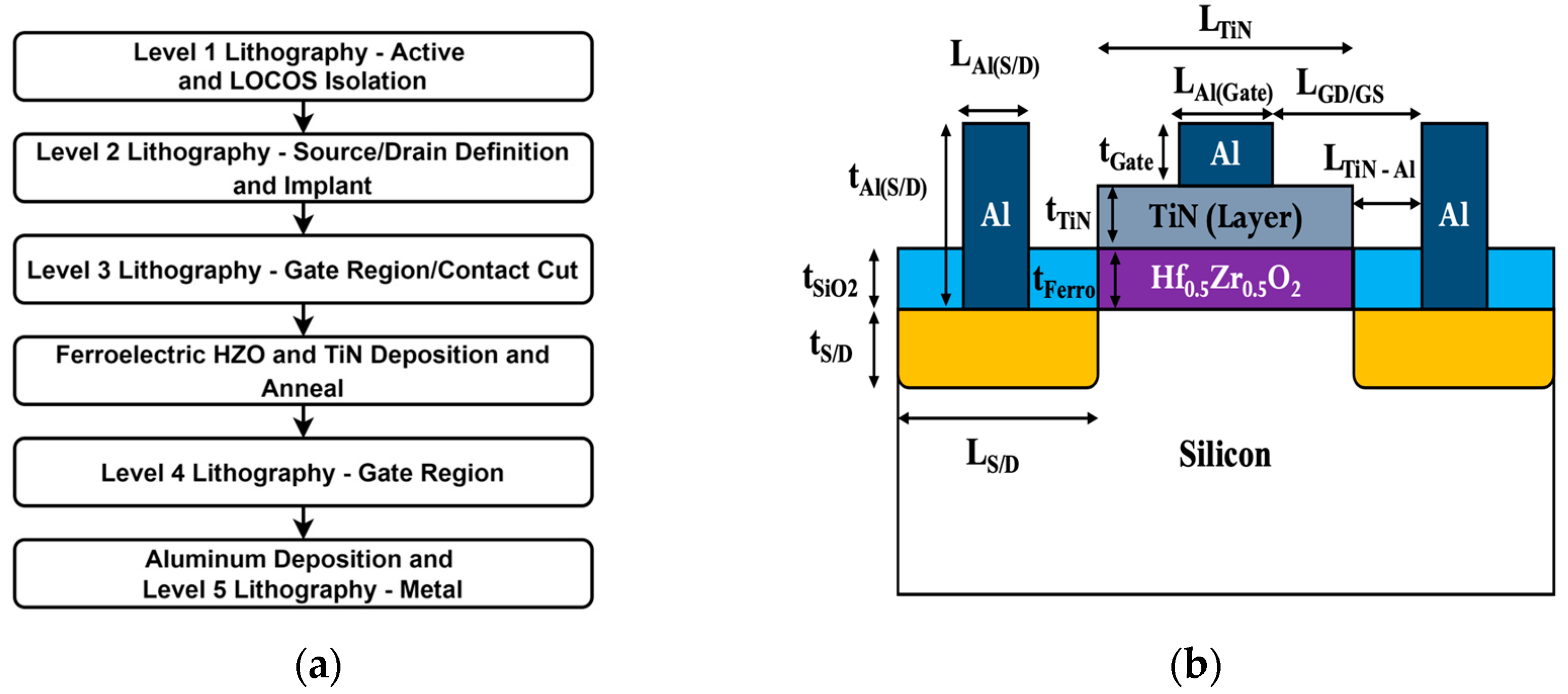
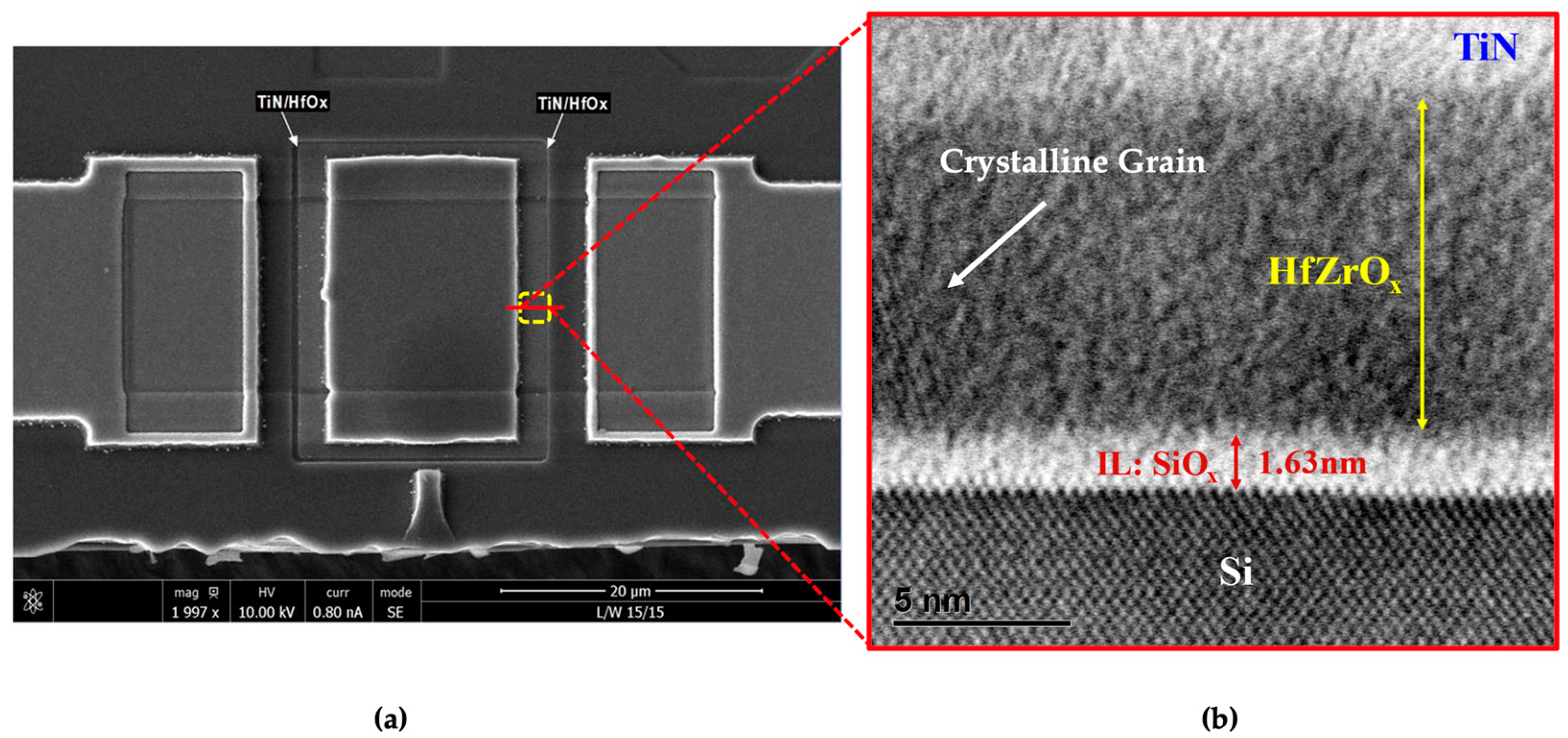
2.1. Experimental

The FeFETs were fabricated in a student run fab [31] at Rochester Institute of Technology (RIT) on 1–10 Ω-cm base resistivity silicon wafers with 10 nm ALD deposited hafnium zirconium oxide (Hf0.5Zr0.5O2) as the gate dielectric and 15 nm of sputtered TiN as the gate electrode, followed by an anneal at 600 °C to achieve the ferroelectric phase. The process flow consisted of 5 mask levels designed in-house using Mentor Graphics Pyxis (v10.2), fabricated by a direct laser writer (DWL 66+, Heidelberg Instruments, Heidelberg, Germany) and using an i-line stepper (PAS 5500, ASML, Veldhoven, Netherlands) for lithography. The devices consisted of LOCOS (local oxidation of silicon) isolated FETs with ion implanted source and drain regions implanted by an ion implanter (350D, Varian Semiconductor Equipment, Gloucester, MA, USA). For the n-channel devices, a P31 implant species and p-type substrates were used, and for the p-channel devices a B11 implant species and n-type substrates were used. The process flow and the device schematics are shown in Figure 2, and a detailed process flow for both n- and p-channel devices can be found in Figures S1 and S2 respectively in the Supplementary Materials.
A scanning electron micrograph image of a fabricated device (with designed 15 µm channel length and 15 μm channel width) and a high-resolution TEM image of the gate dielectric are shown in Figure 3. A close observation of the TEM image reveals the crystalline nature of the deposited ferroelectric HZO (Hf0.5Zr0.5O2) thin film on the silicon substrate. Further, at the HZO/Si interface, a thin interfacial layer (IL) of SiOx (~1.63 nm) is observed.

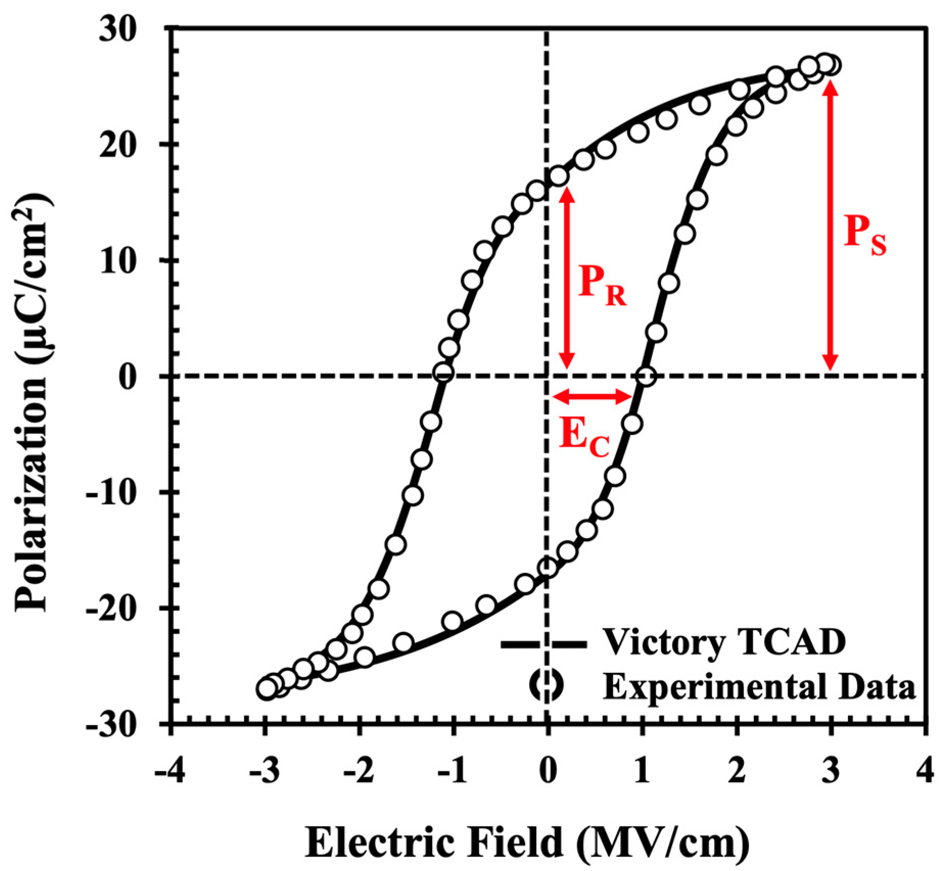
2.2. Polarization Characterization of HZO

The HZO layer employed in this work was characterized for its polarization behavior by fabricating MFM capacitors. The fabricated test structure helps in the assessment and characterization of the deposited thin film ferroelectric layers. The layer stack of the MFM capacitor consists of a bottom electrode deposited by sputtering and standard liftoff procedures to realize a 100 nm TiN layer. This is followed by the conformal atomic layer deposition (ALD) of the 10 nm Hf0.5Zr0.5O2 ferroelectric layer. The top electrode, TiN is then deposited by sputtering.
The polarization-electric field (P-E) hysteresis loop of the test structure were recorded with a parameter analyzer (4200-SCS, Keithley Instruments, Solon, OH, USA), illustrated in Figure 4. As observed, the test structure demonstrates good polarization switching behavior with a remnant polarization (PR) of 17 μC/cm2, saturated polarization (PS) of 27 μC/cm2, and a coercive field (EC) of 1 MV/cm. Also presented is the calibration of a metal-ferroelectric-metal (MFM) capacitor through Silvaco’s Victory TCAD (v 1.22.0) simulator, which will be used as a primer for realizing the fabricated FeFETs through TCAD for further analysis [32]. The TCAD modeling of the MFM capacitor relies on the Preisach Ferroelectric model [33], which utilizes the parameters PR, PS, and EC to model the P-E hysteresis loop as shown in Figure 4.

3. Simulation Methodology

3.1. Experimental Results

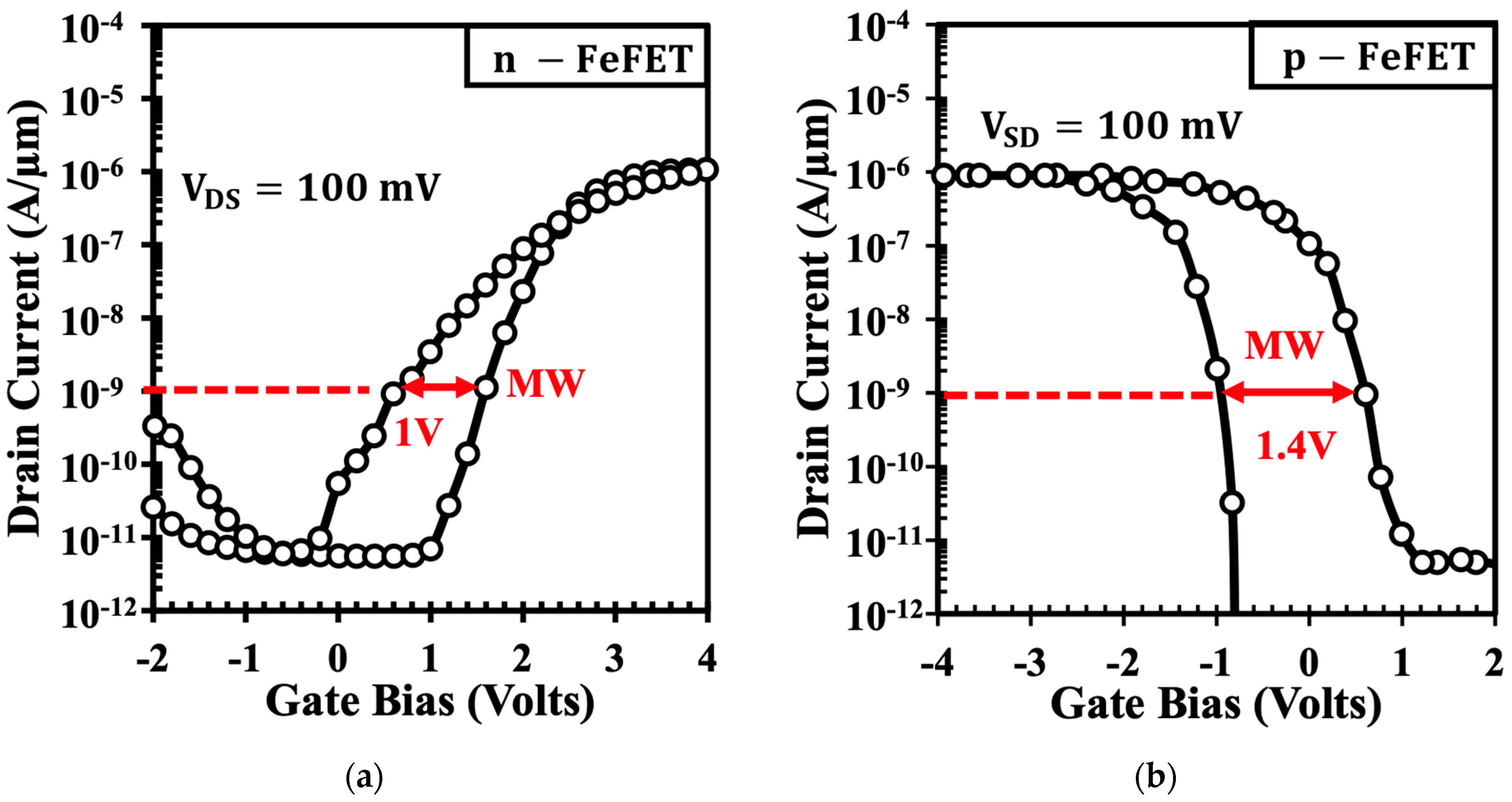
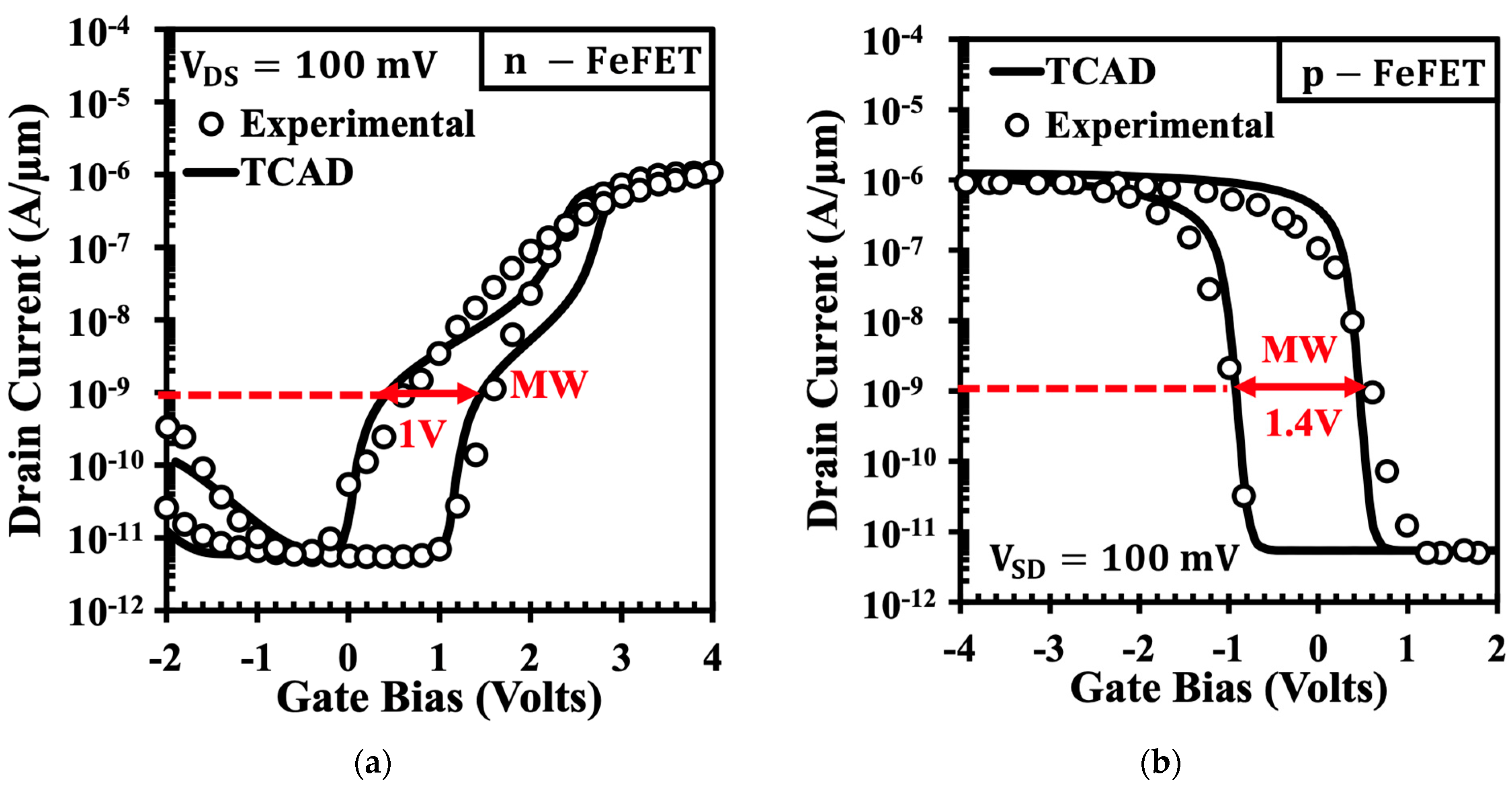
3.1.1. DC Characterization

To investigate the DC characteristics, a parametric analyzer (4200-SCS, Keithley Instruments, Solon, OH, USA) was used. The transfer characteristics (ID vs. VGS) for the n- and p-FeFETs are shown in Figure 5. The memory window (MW) specified at the drain current of 1 nA/µm, and extracted between the high and low VTH states, is observed to be 1 V for the n-FeFET and 1.4 V for the p-FeFET. The DC characteristics of the n- and p-FeFETs demonstrate asymmetric subthreshold characteristics. The p-channel devices exhibit steeper subthreshold characteristics compared to their n-channel counterparts. In addition, the n-FeFETs demonstrate a higher contribution of the gate-induced-drain-leakage (GIDL) current component, suggesting the role of stronger band bending at the accumulation region which is responsible for the setup of high electric fields. This consequently results in the tunneling of the valence band (VB) electrons to the conduction band (CB) while generating holes in the VB, otherwise known as band-to-band tunneling (BTBT). Another distinguishing feature of the n-FeFETs is the characteristic crossover point observed during the downward sweep in the transfer characteristics.

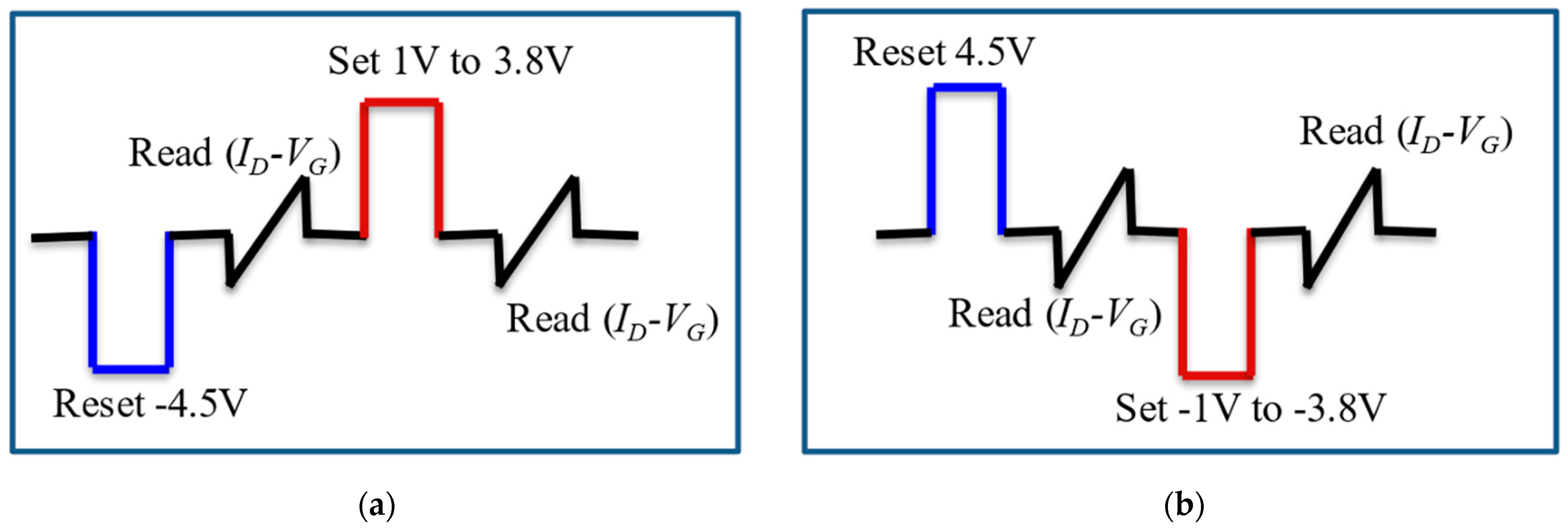
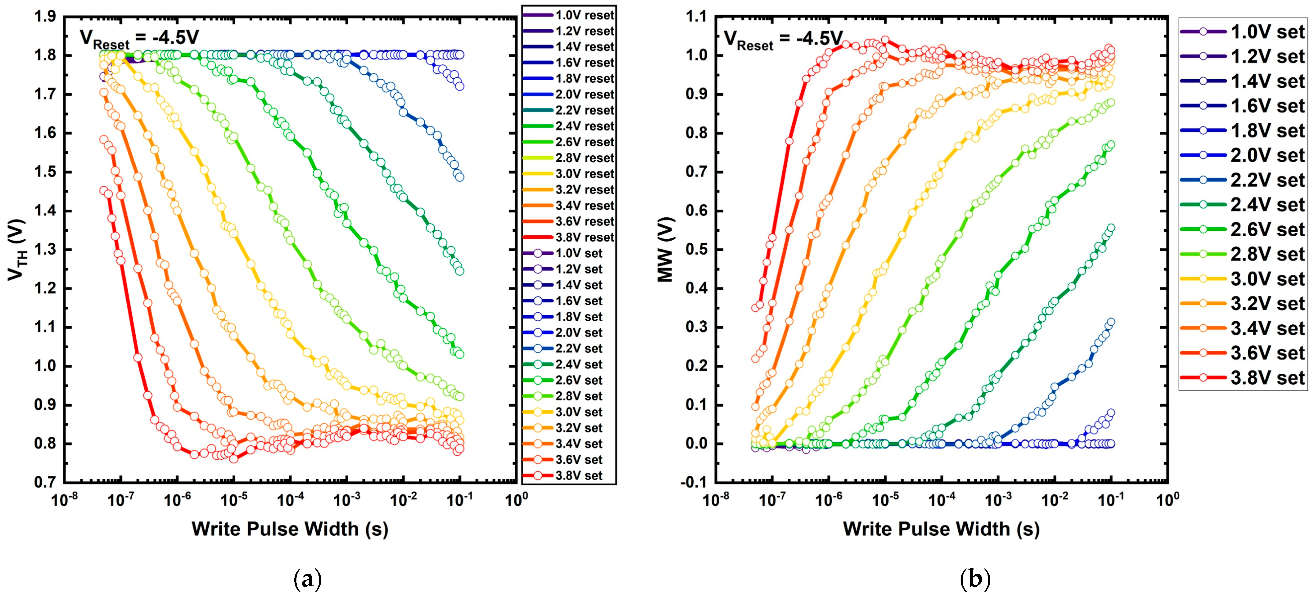
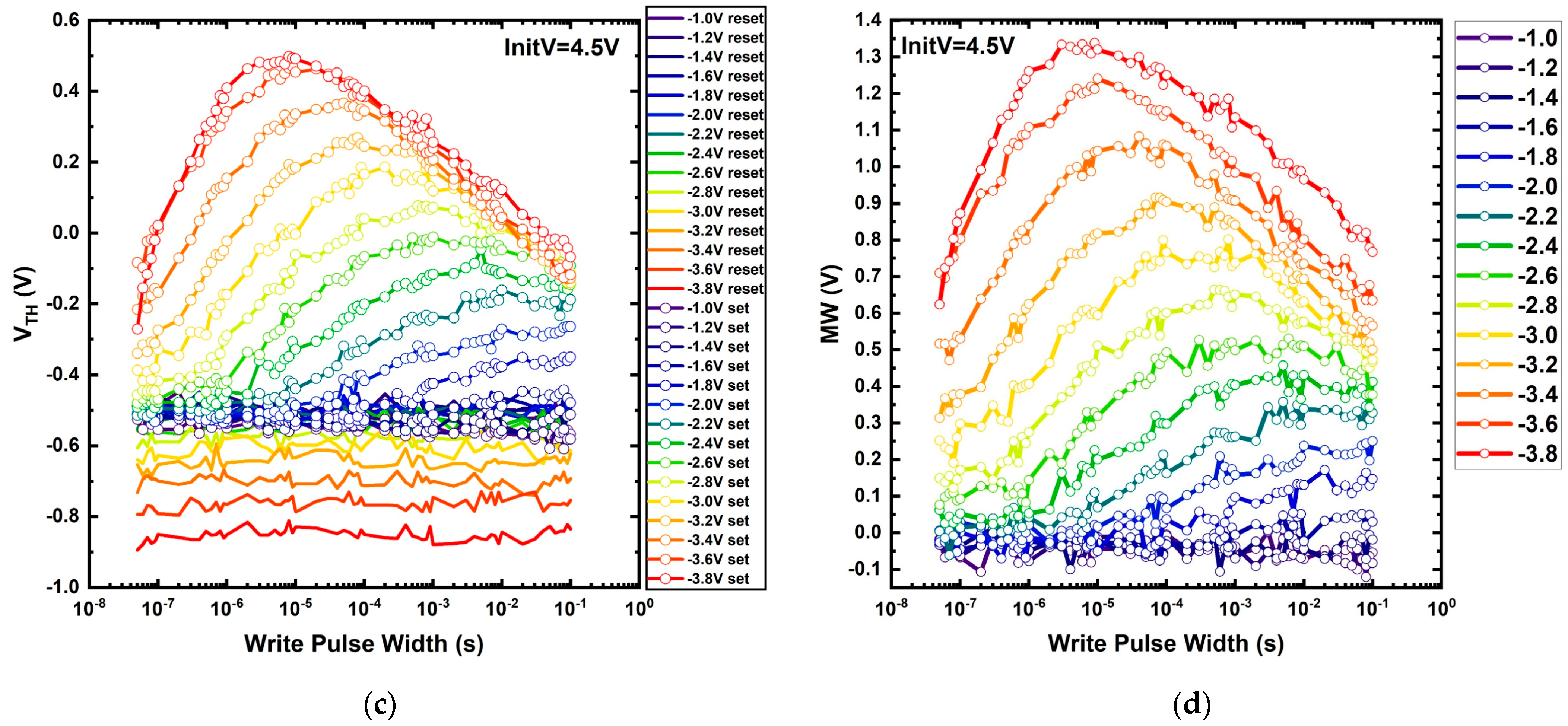
3.1.2. Pulse Characterization

The fabricated n- and p-channel FeFET devices were characterized through a series of read and write pulse cycles using a probe station (Summit 11000/12000, Cascade Microtech, Beaverton, OR, USA) and a parametric analyzer (4200-SCS, Keithley Instruments, Solon, OH, USA). The pulse setups for the n- and p-channel devices are shown in Figure 6. For the n-channel devices, the height of the reset pulse is set to −4.5 V with a pulse duration of 1 μs, while the set pulse height is varied from 1 V to 3.8 V and the pulse duration is gradually tuned from 50 ns to 0.1 s. The p-channel devices are also subjected to similar pulsing conditions with reversed polarities.
The shift in the threshold voltage (VTH) and the resulting MW for the n- and p-channel devices as a function of pulse width is shown in Figure 7. The switching of the polarization dipoles of a particular ferroelectric layer is a function of both the applied bias and the time duration during which the pulse is applied to the ferroelectric gate stack. As observed from Figure 7a,c, the VTH of both devices can be tuned gradually by varying both the pulse height and the pulse duration. As the pulse height decreases, a longer pulse is required for observing the necessary switching of the polarization dipoles. For the n-channel FeFETs, a maximum MW of 1 V, is achieved with a pulse height of 3.8 V and pulse duration of 1 μs, as seen in Figure 7b. This point corresponds to the complete switching of the polarization dipoles within the ferroelectric layer. Intermediate pulse height/widths can be utilized for partial polarization in multi-level logic devices. For the p-channel devices, however, the pulse characteristics in Figure 7c,d demonstrate a global maxima in the MW at a pulse duration of 10 µs and a pulse height of −3.8 V. Further, on increasing the pulse width, a characteristic roll-off in the MW is observed as a function of write pulse width.
The switching behavior investigated using different program/erase pulse heights and widths shows a faster complete polarization switching in n-FeFETs (3.8 V, 1 μs) than in p-FeFETs (−3.8 V, 10 μs).

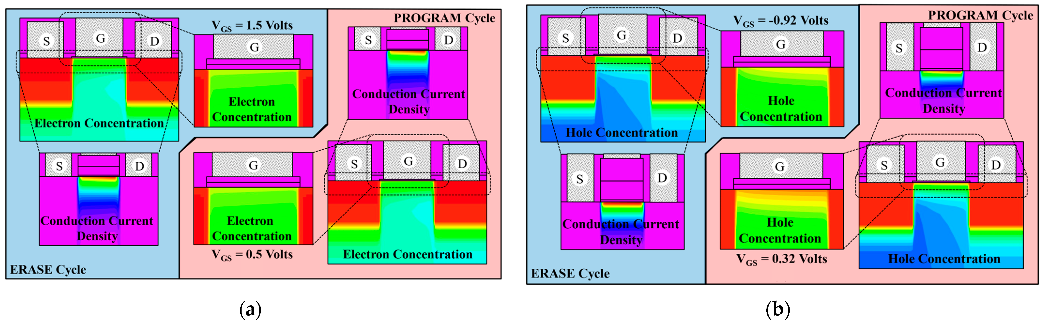
3.2. Simulation Methodology

The polarization parameters extracted from the test structure’s P-E hysteresis loops are fed to the simulation deck to realize ferroelectricity in the HZO. The calibrated simulation deck acts as a primer for realizing FeFET devices for the assessment of the trapping parameters. Table 1 provides the geometrical parameters of the fabricated devices used in simulations.
Silvaco’s Victory Device simulator is used to identify the different kinds of traps that evolved during the fabrication process [27]. A detailed simulation methodology is presented to capture the switching of the polarization dipoles during the upward and downward sweeps.

Calibration of the Fabricated Devices
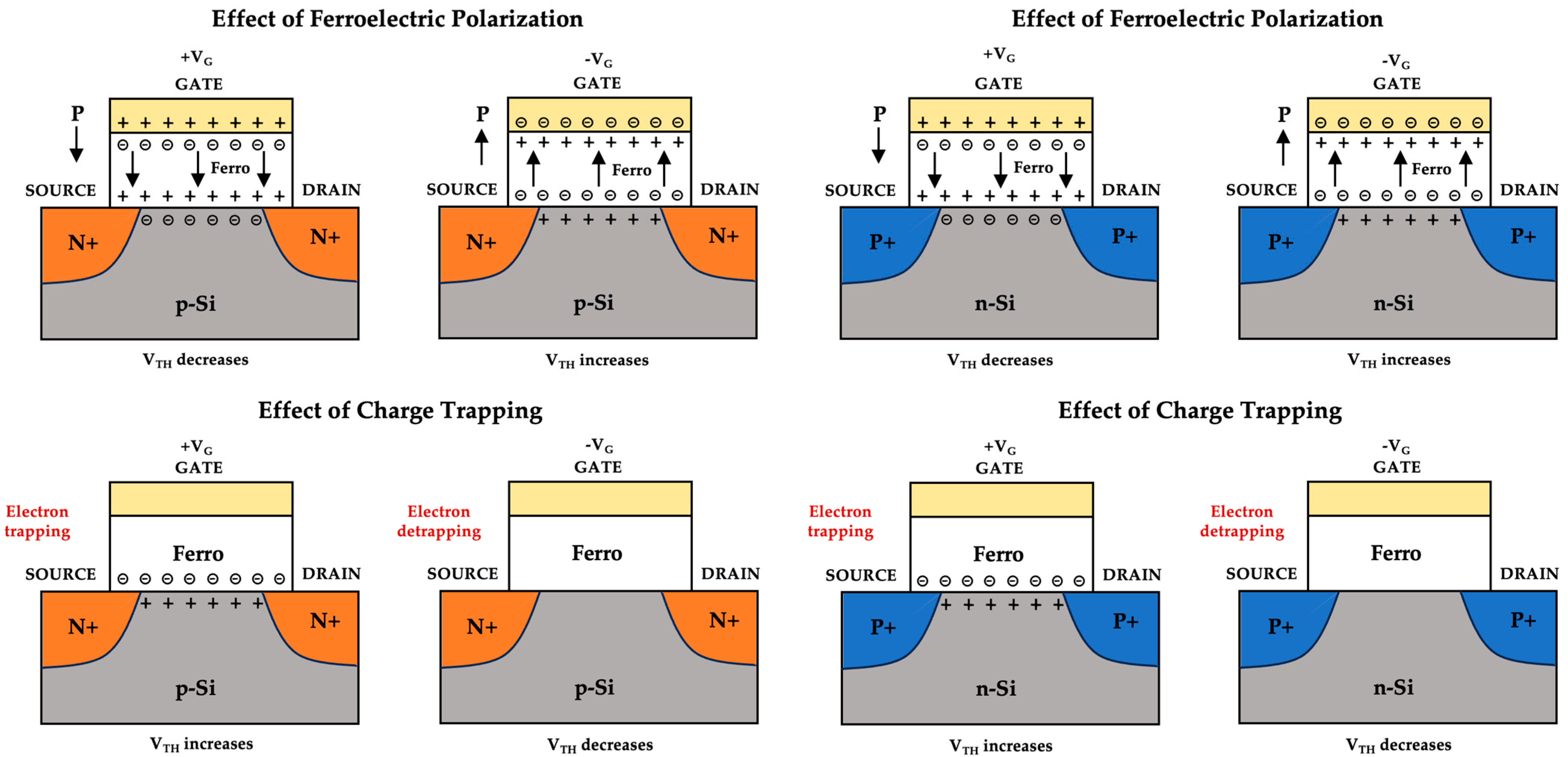
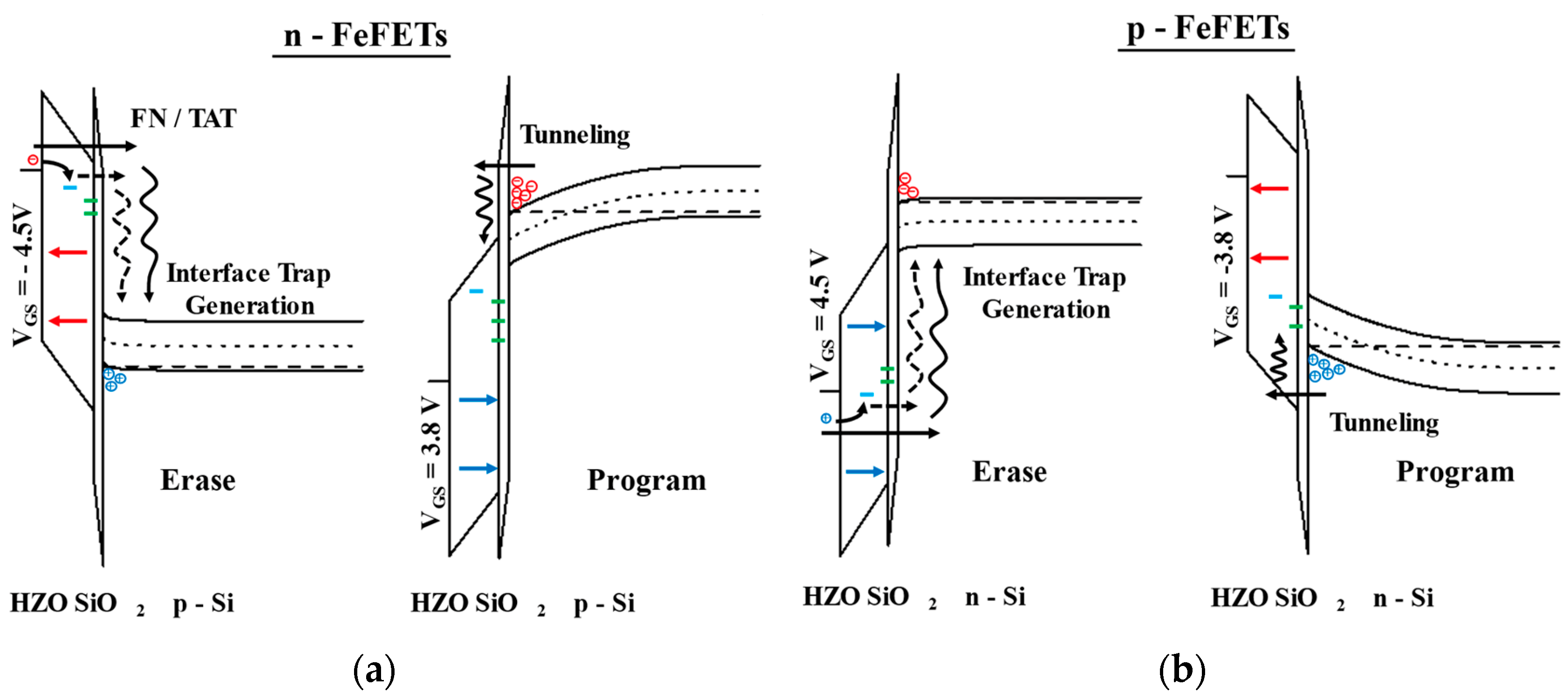
In modeling the fabricated devices, p-channel devices are considered first due to their steeper subthreshold characteristics and a parallel memory window. The off-state current is tuned by considering donor type bulk traps in the silicon substrate. The bulk trap density is set as 1 × 1016 cm3 and the trap level is 0.63 eV. The capture cross section for electrons and holes are set to 10−13 cm2 and 10−14 cm2 respectively in accordance with experimental reports [1,22,34]. Further, the literature survey suggests the role of fixed charges and charge trapping at the HZO/SiO2 interfacial layer (IL) interface in modulating the subthreshold characteristics and thus limiting the memory window of the fabricated devices [1,22,34]. Accordingly, acceptor type interface traps were tuned at the HZO/IL interface to obtain a best fit to the experimental data. In this regard, an interface trap density of 1.8 × 1013 cm2, trap energy level of 0.20 eV and capture cross sections of 10−13 cm2 and 10−14 cm2 for electrons and holes respectively were defined at the HZO/IL interface [33]. In addition to these, Fermi and SRH models were invoked to capture carrier statistics and the interaction of carriers with traps that evolved during the fabrication process. The Priesach Ferroelectric model was also invoked to model the doping dependent mobility, CVT model [35] and to capture the ferroelectric polarization. The calibrated simulation deck for the p-channel device was then used as the basis for realizing n-channel FeFETs. The off-state current was tuned again by considering the donor type bulk traps in the silicon substrate. The trapping conditions defined in the substrate were similar to that of p-channel devices in order to mimic similar bulk conditions, except that the OFF–state current was tuned by changing the energy of the trap level to 0.43 eV. The interface trap density at the HZO/IL interface was similar to the p-channel case, except that the trap levels were tuned to 0.26 eV to capture the slow subthreshold characteristics observed in Figure 5a for n-FeFETs. In addition to this, to capture the GIDL effect observed in n-FeFETs, as seen in Figure 5a, Kane’s BTBT model was invoked, and its coefficients were tuned to achieve the best fit to the GIDL current [30]. The calibrated simulation decks for the n- and p-channel devices are shown in Figure 8.
It is observed that the subthreshold characteristics of n-FeFETs are more affected due to charge trapping at the HZO/SiO2(IL) interface suggesting that electrons are more easily trapped than holes. This observation essentially stems from the transfer characteristics of the fabricated n- and p-channel FeFET devices. As observed from the subthreshold characteristics of both Figure 5a and Figure 8a, the n-channel FeFET devices demonstrate a gradual change (along with kink) in the subthreshold characteristics, which is a characteristic feature of the trapping and detrapping of the majority carriers, which for the n-channel devices are electrons. On the contrary, for the p-channel devices, as observed from both Figure 5b and Figure 8b, the transfer characteristics, particularly in the subthreshold region demonstrate a steep change with the applied bias without any significant trapping effects as far as the DC characteristics are concerned. From a TCAD perspective, this is achieved by favoring electron trapping by specifying a larger capture cross section area as discussed above and validated from the TCAD simulations shown in Figure 8a. The presence of IL further participates in a tunneling current, due to charge trapping at the HZO/SiO2 (IL). This results in a charge transfer directly between the HZO and Si channel and is responsible for modulating the subthreshold characteristics of the n-FeFETs [36].
The characteristic crossover point observed in the n-channel devices during the downward sweep was also captured in the TCAD simulations, as shown in Figure 8a. A closer insight into this reveals that there is a temporary switching of the ferroelectric based operation to the charged based operation, which arises due to the presence of the fixed charges and charge trapping at the HZO/IL interface and HZO bulk layer. Under this condition, during the negative sweep, the drain current characteristics are dominated by the carrier trapping which reduces the ON—state current (shown in Figure 8a) as the applied bias is reduced from 4 V to 2 V (denoted as the charge-based operation). The trapped carriers are detrapped as the applied bias is further reduced beyond 2 V, after which, the ferroelectric based operation dominates, giving rise to the memory window (MW) as observed in Figure 8a.
The devices are further investigated by recording the contour plots of electron/hole concentrations and conduction current densities after forward and reverse sweeps at 1 nA/μm. These are depicted in Figure 9a for n-FeFETs and in Figure 9b for p-FeFETs. For the n-channel device, as observed from Figure 9a, the shift in electron concentration and conduction current density is not significant after the respective program/erase cycles. In contrast, for the p-channel device, a significant change in both the hole concentration as well as the conduction current density is observed in Figure 9b, which accounts for the shift in VTH observed in both Figure 7c,d and Figure 5b after subjecting the gate stack to the necessary program cycle.
The trapping effects on the MW can be understood by observing the band diagrams recorded at erase and program conditions. This is shown in Figure 10a,b for the n- and p-channel devices, respectively. For the n-FeFET devices, as depicted in Figure 10a, the carriers can directly tunnel through the HZO and the IL (SiO2) through Fowler-Nordheim (FN) tunneling [37]. The carriers can also participate in tunneling with the help of acceptor type traps defined at the HZO/IL interface and at the HZO bulk through the trap-assisted tunneling (TAT) [37]. The injected carriers are ‘hot’, in the sense that these carriers are energetic and can further participate in the generation of interface traps at the SiO2 (IL)/Si interface, thereby degrading the quality of the memory window or the devices over time. Consequently, there is a charge sharing directly between the HZO and the silicon channel, which is responsible for modulating the subthreshold characteristics observed in Figure 5a and Figure 8a. Under the program cycle, as depicted in Figure 10b, the electron carriers tunnel through the SiO2 layer, which is translated to the shift observed in the device threshold voltage. Further, on observing the position of the traps with respect to the fermi level under both erase and program conditions, as seen in Figure 10a, it can be inferred that most of the tunneled carriers during the program pulse are trapped courtesy of the bulk traps in HZO and at HZO/IL interface. Consequently, the span of the memory window for the n-FeFETs gets limited.
The band diagrams under erase/program conditions depicted in Figure 10b for p-channel devices follow a similar approach. The tunneling probabilities for the holes, however, is much lower than that of the electrons and the charge sharing through FN/TAT is effectively minimized. At a sufficiently higher gate bias, there is still a possibility of ‘hot’ hole injection, which may result in the generation of traps at the SiO2/Si interface. Under the program cycle, similar to the n-channel case, the tunneling of the hole carriers through the SiO2 is responsible for the shift in the device threshold voltage observed in Figure 5b and Figure 8b. Further, it is also identified that there are multi-level traps present at the HZO/IL interface. These traps are relatively deeper, as discussed in Section 3.1.1, and are responsible for the roll-off in the device VTH observed during the pulse characterization of the p-FeFET devices in Figure 7c.

4. Discussion

In this work, n-FeFETs and p-FeFET devices have been designed, fabricated and investigated using a similar process flow, which is important for their integration in CMOS circuitry. A systematic and calibrated TCAD study is presented to investigate trapping effects on the asymmetric behavior observed in the transfer and pulse characteristics of n- and p-channel FeFET devices. For model validation, fabricated MFM capacitors are realized, and the P-E hysteresis loops are calibrated against the experimental set. The calibrated deck is then used to model the FeFETs to identify the trapping parameters. The n-FeFETs demonstrate faster complete polarization switching compared to their p-channel counterparts. It has been observed that the fixed charges and interface traps at HZO/IL modulate the subthreshold characteristics of the fabricated FeFETs and are responsible for the asymmetricity observed in the transfer characteristics of the two devices. Further, the IL facilitates the tunneling current due to the presence of traps in the bulk HZO and at HZO/IL. This is responsible for the charge sharing directly between the HZO and the silicon channel and limits the span of the memory window for the fabricated devices. The n-channel devices, as observed, are identified to be more affected compared to p-channel devices, suggesting that electrons are more easily trapped than holes. Further, the characteristic crossover point observed in n-FeFETs was found to be associated with the partial recovery of the polarization dipoles due to the charge trapping mechanism, which results in a temporary switch between ferroelectric based operation to charge based operation.

Supplementary Materials

The following supporting information can be downloaded at: https://www.mdpi.com/article/10.3390/solids4040023/s1, Figure S1: Process Flow for fabrication of n-FeFETs, Figure S2: Process Flow for fabrication of p-FeFETs.

Author Contributions

Conceptualization, S.K.; methodology, S.K., P.J. and P.C.P.; software, M.S., K.S. and M.G.; validation, D.M., K.N. and S.D.; formal analysis, P.J., K.S., K.N. and S.D.; investigation, P.J., K.N. and S.K.; resources, S.K. and K.N.; data curation, P.J. and S.K.; writing—original draft preparation, K.S., P.J. and S.K.; writing—review and editing, P.J. and S.K.; visualization, K.N., D.M. and S.D.; supervision, S.K.; project administration, S.K.; funding acquisition, S.K. All authors have read and agreed to the published version of the manuscript.

Funding

The authors acknowledge the support of Semiconductor Research Corporation (SRC) under GRC Projects 2825.001 and 2020-LM-2999. This work was also supported in part by the National Science Foundation, Grant #EEC-2123863. Any opinions, findings, and conclusions or recommendations expressed in this material are those of the author(s) and do not necessarily reflect the views of the National Science Foundation.

Data Availability Statement

All data are available upon request from the corresponding author.

Acknowledgments

The authors acknowledge Uwe Schroeder and Claudia Richter of Nanoelectronic Materials Laboratory (NaMLab), gGmbH for their support in HZO deposition.

Conflicts of Interest

The funding sponsors had no role in the design of the study; in the collection, analyses, or interpretation of data; in the writing of the manuscript, and in the decision to publish the results.

References

  1. Kim, J.Y.; Choi, M.-J.; Jang, H.W. Ferroelectric Field Effect Transistors: Progress and Perspective. APL Mater. 2021, 9, 021102. [Google Scholar] [CrossRef]
  2. Mulaosmanovic, H.; Ocker, J.; Müller, S.; Noack, M.; Müller, J.; Polakowski, P.; Mikolajick, T.; Slesazeck, S. Novel Ferroelectric FET Based Synapse for Neuromorphic Systems. In Proceedings of the 2017 Symposium on VLSI Technology, Kyoto, Japan, 5–8 June 2017; IEEE: Piscataway, NJ, USA, 2017; pp. T176–T177. [Google Scholar]
  3. Mulaosmanovic, H.; Chicca, E.; Bertele, M.; Mikolajick, T.; Slesazeck, S. Mimicking Biological Neurons with a Nanoscale Ferroelectric Transistor. Nanoscale 2018, 10, 21755–21763. [Google Scholar] [CrossRef]
  4. Ni, Y.; Wang, Y.; Xu, W. Recent Process of Flexible Transistor-structured Memory. Small 2021, 17, 1905332. [Google Scholar] [CrossRef] [PubMed]
  5. Han, S.-T.; Zhou, Y. Photo-Electroactive Non-Volatile Memories for Data Storage and Neuromorphic Computing; Woodhead Publishing: Cambridge, UK, 2020; ISBN 0128226064. [Google Scholar]
  6. Yoon, S.-K.; Youn, Y.-S.; Kim, J.-G.; Kim, S.-D. Design of DRAM-NAND Flash Hybrid Main Memory and Q-Learning-Based Prefetching Method. J. Supercomput. 2018, 74, 5293–5313. [Google Scholar] [CrossRef]
  7. Mogul, J.C.; Argollo, E.; Shah, M.A.; Faraboschi, P. Operating System Support for NVM+ DRAM Hybrid Main Memory. In Proceedings of the HotOS, Monte Verità, Switzerland, 18–20 May 2009; Volume 9, p. 14. [Google Scholar]
  8. Ali, T.; Mertens, K.; Kühnel, K.; Rudolph, M.; Oehler, S.; Lehninger, D.; Müller, F.; Revello, R.; Hoffmann, R.; Zimmermann, K. A FeFET with a Novel MFMFIS Gate Stack: Towards Energy-Efficient and Ultrafast NVMs for Neuromorphic Computing. Nanotechnology 2021, 32, 425201. [Google Scholar] [CrossRef] [PubMed]
  9. Hahnloser, R.H.R.; Sarpeshkar, R.; Mahowald, M.A.; Douglas, R.J.; Seung, H.S. Digital Selection and Analogue Amplification Coexist in a Cortex-Inspired Silicon Circuit. Nature 2000, 405, 947–951. [Google Scholar] [CrossRef] [PubMed]
  10. Park, Y.; Kim, M.-K.; Lee, J.-S. Emerging Memory Devices for Artificial Synapses. J. Mater. Chem. C Mater. 2020, 8, 9163–9183. [Google Scholar] [CrossRef]
  11. Merolla, P.A.; Arthur, J.V.; Alvarez-Icaza, R.; Cassidy, A.S.; Sawada, J.; Akopyan, F.; Jackson, B.L.; Imam, N.; Guo, C.; Nakamura, Y. A Million Spiking-Neuron Integrated Circuit with a Scalable Communication Network and Interface. Science 2014, 345, 668–673. [Google Scholar] [CrossRef]
  12. Isupov, V.A. Phases in the PZT Ceramics. Ferroelectrics 2002, 266, 91–102. [Google Scholar] [CrossRef]
  13. Chung, C.-C. Microstructural Evolution in Lead Zirconate Titanate (PZT) Piezoelectric Ceramics. Ph.D. Thesis, University of Connecticut, Storrs, CT, USA, 2014. [Google Scholar]
  14. Bhalla, A.S.; Guo, R.; Alberta, E.F. Some Comments on the Morphotropic Phase Boundary and Property Diagrams in Ferroelectric Relaxor Systems. Mater. Lett. 2002, 54, 264–268. [Google Scholar] [CrossRef]
  15. Zhu, H.; Yamamoto, S.; Matsui, J.; Miyashita, T.; Mitsuishi, M. Resistive Non-Volatile Memories Fabricated with Poly (Vinylidene Fluoride)/Poly (Thiophene) Blend Nanosheets. RSC Adv. 2018, 8, 7963–7968. [Google Scholar] [CrossRef] [PubMed]
  16. Furukawa, T. Ferroelectric Properties of Vinylidene Fluoride Copolymers. Phase Transit. Multinatl. J. 1989, 18, 143–211. [Google Scholar] [CrossRef]
  17. Wang, J.; Li, H.; Liu, J.; Duan, Y.; Jiang, S.; Yan, S. On the A→ β Transition of Carbon-Coated Highly Oriented PVDF Ultrathin Film Induced by Melt Recrystallization. J. Am. Chem. Soc. 2003, 125, 1496–1497. [Google Scholar] [CrossRef] [PubMed]
  18. Lovinger, A.J. Unit Cell of the γ Phase of Poly (Vinylidene Fluoride). Macromolecules 1981, 14, 322–325. [Google Scholar] [CrossRef]
  19. Kim, S.J.; Mohan, J.; Lee, J.; Lee, J.S.; Lucero, A.T.; Young, C.D.; Colombo, L.; Summerfelt, S.R.; San, T.; Kim, J. Effect of Film Thickness on the Ferroelectric and Dielectric Properties of Low-Temperature (400 °C) Hf0.5Zr0.5O2 Films. Appl. Phys. Lett. 2018, 112, 172902. [Google Scholar] [CrossRef]
  20. Böscke, T.S.; Müller, J.; Bräuhaus, D.; Schröder, U.; Böttger, U. Ferroelectricity in Hafnium Oxide Thin Films. Appl. Phys. Lett. 2011, 99, 102903. [Google Scholar] [CrossRef]
  21. Kim, S.J.; Mohan, J.; Summerfelt, S.R.; Kim, J. Ferroelectric Hf0.5Zr0.5O2 Thin Films: A Review of Recent Advances. JOM 2019, 71, 246–255. [Google Scholar] [CrossRef]
  22. Ni, K.; Sharma, P.; Zhang, J.; Jerry, M.; Smith, J.A.; Tapily, K.; Clark, R.; Mahapatra, S.; Datta, S. Critical Role of Interlayer in Hf0.5Zr0.5O2 Ferroelectric FET Nonvolatile Memory Performance. IEEE Trans. Electron Devices 2018, 65, 2461–2469. [Google Scholar] [CrossRef]
  23. Park, M.H.; Lee, Y.H.; Kim, H.J.; Kim, Y.J.; Moon, T.; Kim, K.D.; Mueller, J.; Kersch, A.; Schroeder, U.; Mikolajick, T. Ferroelectricity and Antiferroelectricity of Doped Thin HfO2-based Films. Adv. Mater. 2015, 27, 1811–1831. [Google Scholar] [CrossRef]
  24. Sharma, P.; Tapily, K.; Saha, A.K.; Zhang, J.; Shaughnessy, A.; Aziz, A.; Snider, G.L.; Gupta, S.; Clark, R.D.; Datta, S. Impact of Total and Partial Dipole Switching on the Switching Slope of Gate-Last Negative Capacitance FETs with Ferroelectric Hafnium Zirconium Oxide Gate Stack. In Proceedings of the 2017 Symposium on VLSI Technology, Kyoto, Japan, 5–8 June 2017; IEEE: Piscataway, NJ, USA, 2017; pp. T154–T155. [Google Scholar]
  25. Lomenzo, P.D.; Jachalke, S.; Stoecker, H.; Mehner, E.; Richter, C.; Mikolajick, T.; Schroeder, U. Universal Curie Constant and Pyroelectricity in Doped Ferroelectric HfO2 Thin Films. Nano Energy 2020, 74, 104733. [Google Scholar] [CrossRef]
  26. Anderson, J.D.; Merkel, J.; Macmahon, D.; Kurinec, S.K. Evaluation of Si: HfO2 Ferroelectric Properties in MFM and MFIS Structures. IEEE J. Electron Devices Soc. 2018, 6, 525–534. [Google Scholar] [CrossRef]
  27. Yurchuk, E.; Müller, J.; Müller, S.; Paul, J.; Pešić, M.; van Bentum, R.; Schroeder, U.; Mikolajick, T. Charge-Trapping Phenomena in HfO2-Based FeFET-Type Nonvolatile Memories. IEEE Trans. Electron Devices 2016, 63, 3501–3507. [Google Scholar] [CrossRef]
  28. Deng, S.; Jiang, Z.; Dutta, S.; Ye, H.; Chakraborty, W.; Kurinec, S.; Datta, S.; Ni, K. Examination of the Interplay between Polarization Switching and Charge Trapping in Ferroelectric FET. In Proceedings of the 2020 IEEE International Electron Devices Meeting (IEDM), San Francisco, CA, USA, 12–18 December 2020; IEEE: Piscataway, NJ, USA, 2020; p. 4. [Google Scholar]
  29. Izmailov, R.A.; Strand, J.W.; Larcher, L.; O’Sullivan, B.J.; Shluger, A.L.; Afanas’ev, V.V. Electron Trapping in Ferroelectric HfO2. Phys. Rev. Mater. 2021, 5, 034415. [Google Scholar] [CrossRef]
  30. Lue, H.-T.; Wu, C.-J.; Tseng, T.-Y. Device Modeling of Ferroelectric Memory Field-Effect Transistor (FeMFET). IEEE Trans. Electron Devices 2002, 49, 1790–1798. [Google Scholar]
  31. RIT Semiconductor & Microsystems Fabrication Laboratory. Available online: https://www.rit.edu/facilities/semiconductor-and-microsystems-fabrication-laboratory (accessed on 30 September 2023).
  32. Silvaco Inc., S.C.U. Victory Device User’s Manual; Silvaco Inc., S.C.U.: Santa Clara, CA, USA, 2015. [Google Scholar]
  33. Kuzum, D.; Park, J.-H.; Krishnamohan, T.; Wong, H.-S.P.; Saraswat, K.C. The Effect of Donor/Acceptor Nature of Interface Traps on Ge MOSFET Characteristics. IEEE Trans. Electron Devices 2011, 58, 1015–1022. [Google Scholar] [CrossRef]
  34. Bae, H.; Nam, S.G.; Moon, T.; Lee, Y.; Jo, S.; Choe, D.-H.; Kim, S.; Lee, K.-H.; Heo, J. Sub-Ns Polarization Switching in 25 nm FE FinFET toward Post CPU and Spatial-Energetic Mapping of Traps for Enhanced Endurance. In Proceedings of the 2020 IEEE International Electron Devices Meeting (IEDM), San Francisco, CA, USA, 12–18 December 2020; IEEE: Piscataway, NJ, USA, 2020; pp. 31–33. [Google Scholar]
  35. Lombardi, C.; Manzini, S.; Saporito, A.; Vanzi, M. A Physically Based Mobility Model for Numerical Simulation of Nonplanar Devices. IEEE Trans. Comput.-Aided Des. Integr. Circuits Syst. 1988, 7, 1164–1171. [Google Scholar] [CrossRef]
  36. Mittmann, T.; Materano, M.; Chang, S.-C.; Karpov, I.; Mikolajick, T.; Schroeder, U. Impact of Oxygen Vacancy Content in Ferroelectric HZO Films on the Device Performance. In Proceedings of the 2020 IEEE International Electron Devices Meeting (IEDM), San Francisco, CA, USA, 12–18 December 2020; IEEE: Piscataway, NJ, USA, 2020; pp. 14–18. [Google Scholar]
  37. Khan, A.I.; Keshavarzi, A.; Datta, S. The Future of Ferroelectric Field-Effect Transistor Technology. Nat. Electron. 2020, 3, 588–597. [Google Scholar] [CrossRef]
Figure 1. Effect of polarization switching and charge trapping on the threshold voltage shift in MOSFETs.
Solids 04 00023 g001
Figure 2. (a) Process flow for the fabrication of FeFETs, and (b) Schematic diagram of a fabricated FeFET.
Solids 04 00023 g002
Figure 3. (a) SEM image of a FeFET (top view), and (b) Cross-sectional TEM image of the gate stack.
Solids 04 00023 g003
Figure 4. Measured and simulated polarization-electric field hysteresis loop of TiN/10 nm HZO/TiN capacitor.
Solids 04 00023 g004
Figure 5. Transfer characteristics of (a) n-channel FeFETs, and (b) p-channel FeFETs depicting asymmetric behavior.
Solids 04 00023 g005
Figure 6. Read and write operations performed at the gate electrode of (a) n-FeFET, and (b) p-FeFET.
Solids 04 00023 g006
Figure 7. Partial polarization switching by varying the pulse width: (a) Gradual tuning of VTH, and (b) MW for n-channel, (c) Gradual tuning of VTH, and (d) MW for p-channel by increasing the width of the program pulse.
Solids 04 00023 g007aSolids 04 00023 g007b
Figure 8. Calibration of simulation deck in Silvaco’s Victory TCAD for (a) n-channel, and (b) p-channel FeFETs.
Solids 04 00023 g008
Figure 9. Depiction of electron/hole concentration and conduction current density contour plots for (a) n-FeFETs, and (b) p-FeFETs.
Solids 04 00023 g009
Figure 10. Band diagrams under erase and program conditions for (a) n-FeFETs, and (b) p-FeFETs. Red and Blue Arrows (/) in the SiO2 dictate the orientation of the polarization field, the Black Arrow (→) dictates the tunneling direction, while the green and blue symbols (-/-) represent the traps in bulk HZO and HZO/IL interface.
Solids 04 00023 g010
Table 1. Device geometrical parameters depicted in Figure 2b.
SymbolsDescriptionValue
ND/SSource/Drain Doping2 × 1019 cm−3
NSubsSubstrate Doping2 × 1015 cm−3
tS/DJunction depth of Source/Drain0.8 µm
LS/DLateral Extensions of Source/Drain13 µm
tSiO2Thickness of Silicon Dioxide100 nm
tFerroThickness of Ferro Layer10 nm
tTiNThickness of TiN Layer12 nm
tGateThickness of Al Gate Contact750 nm
tAl(S/D)Thickness of Al Source/Drain Contact750 nm
LAl(S/D)Length of Al Source/Drain Contact9 µm
Disclaimer/Publisher’s Note: The statements, opinions and data contained in all publications are solely those of the individual author(s) and contributor(s) and not of MDPI and/or the editor(s). MDPI and/or the editor(s) disclaim responsibility for any injury to people or property resulting from any ideas, methods, instructions or products referred to in the content.

