Article

The Origin of the Yellow Luminescence Band in Be-Doped Bulk GaN

by
Michael A. Reshchikov
1,* and
Michal Bockowski
2
1
Department of Physics, Virginia Commonwealth University, Richmond, VA 23220, USA
2
Institute of High Pressure Physics, Polish Academy of Sciences, Sokolowska 29/37, 01-142 Warsaw, Poland
*
Author to whom correspondence should be addressed.
Solids 2024, 5(1), 29-44; https://doi.org/10.3390/solids5010003
Submission received: 19 November 2023 / Revised: 29 December 2023 / Accepted: 1 January 2024 / Published: 4 January 2024

Abstract

:
Photoluminescence (PL) from Be-doped bulk GaN crystals grown by the High Nitrogen Pressure Solution method was studied and compared with PL from GaN:Be layers on sapphire grown by molecular beam epitaxy and metalorganic chemical vapor deposition techniques. The yellow luminescence band in the latter is caused by the isolated BeGa acceptor (the YLBe band), while the broad yellow band in bulk GaN:Be crystals is a superposition of the YLBe band and another band, most likely the CN-related YL1 band. The attribution of the yellow band in bulk GaN:Be crystals to the BeGaON complex (a deep donor) is questioned.

1. Introduction

GaN with a bandgap of 3.50 eV attracts significant attention from researchers due to its applications in light-emitting and high-power devices [1,2,3,4]. Point defects that may detrimentally affect the devices’ efficiency and longevity are still poorly understood. Photoluminescence (PL) is a powerful research tool that reveals the properties of point defects, such as charge state, transition levels, and carrier capture coefficients [5,6,7].
The most-studied defect-related PL band in GaN is the yellow luminescence (YL) band [8,9,10]. In undoped GaN grown by metalorganic chemical vapor deposition (MOCVD), the YL band with a maximum at 2.17 eV and zero-phonon line (ZPL) at 2.59 eV (labeled the YL1 band) is commonly observed due to contamination with carbon and attributed to the CN acceptor [10,11,12,13,14]. The YL1 band can also be recognized in PL spectra from undoped GaN grown by other techniques such as the High Nitrogen Pressure Solution (HNPS) method [15] and the hydride vapor phase epitaxy (HVPE) method [12]. Very low concentrations of carbon (1015–1016 cm−3) in HVPE-grown undoped GaN lead to the quantum efficiency of the YL1 band close to unity thanks to a relatively high hole-capture cross-section of the CN defect [16,17]. This explains why the CN-related YL1 band is omnipresent in undoped GaN and GaN doped with various impurities.
A different (as will be shown below) yellow band is observed in GaN doped or implanted with beryllium (Be) [9,17,18,19]. A renewed interest in doping III-nitrides with Be is fueled by recent findings that shallow Be-related acceptors can potentially be used for conductive p-type GaN and AlN [20,21,22]. We recently studied PL from more than 100 Be-doped GaN samples grown by MOCVD and molecular beam epitaxy (MBE), as well as GaN samples grown by HVPE and implanted with Be or co-implanted with Be and F [23,24]. In almost all these samples, the YL band is the dominant defect-related PL band with absolute internal quantum efficiency approaching unity in some samples. This YL band, with a maximum at 2.15 eV and specific properties (labeled the YLBe band), is now reliably attributed to the isolated BeGa acceptor [25].
In fair agreement with the theoretical predictions of Lany and Zunger [26], deep and shallow states of the BeGa acceptor are found in PL experiments [25]. Two deep polaronic configurations with a hole localized at a neighboring N atom in the c direction and one of three other directions have −/0 transition levels at 0.38 ± 0.03 eV (configuration Be2) and 0.33 ± 0.05 eV (Be1), respectively, above the valence band maximum (VBM) in the limit of low temperatures. Electron transitions from the conduction band to these levels are responsible for the YLBe2 and YLBe1 components of the YLBe band, respectively [25]. The shallow state with a delocalized hole (Be3) is at 0.24 ± 0.02 eV above the VBM. Electron transitions from the conduction band to the shallow level cause the ultraviolet luminescence (UVL) band, with the main peak at 3.26 eV (labeled the UVLBe3). Although the UVLBe3 band resembles the Mg-related UVL band (the UVLMg band with the main peak at 3.28 eV), these two bands can be reliably distinguished thanks to their specific temperature dependences [25]. In particular, the ratio of intensities of the UVLBe3 and YLBe2 bands, IUVLBe3/IYLBe2, is the same for all GaN:Be samples, and it can be fitted with the following expression:
I B e 3 U V L I B e 2 Y L = δ exp Δ E k T ,
where δ is approximately equal to the ratio of the electron-capture coefficients for the Be3 and Be2 states of the BeGa acceptor (18 ± 8) and ΔE is the energy difference between these states (140 ± 10 meV). This property allows us to reliably recognize PL from the BeGa acceptor in GaN:Be samples, even when other PL bands contribute to the PL spectrum.
Another unique feature of the YLBe band (observed in all studied GaN:Be layers on sapphire) is two-step quenching and complete disappearance at temperatures close to room temperature. The first step at about 100 K is attributed to a replacement of the YLBe1 component by the YLBe2 component after a captured hole transits from Be1 to Be2 over a potential barrier. The second quenching begins at about 200 K. The activation energy of this quenching is 0.30 eV in n-type samples, which led us to erroneously assume that the quenching is caused by the thermal emission of holes from the deep polaronic state to the valence band [23]. However, a more detailed analysis indicated that the quenching is caused by the thermal emission of holes from the shallow BeGa state (Be3, at ~0.20 eV at these temperatures) to the valence band. The larger nominal activation energy and relatively high temperatures at which the quenching of PL from such a shallow level occurs are explained by the feeding mechanism [25]. Namely, holes from the deep polaronic state are excited to the shallow state before they escape to the valence band, so that the measured activation energy of the quenching is the sum of the shallow state energy (E3) and the energy difference between the shallow and deep states (ΔE).
A similar and very bright YL band with a maximum at 2.1–2.2 eV is observed in bulk GaN:Be crystals produced by the HNPS growth method [27,28,29]. However, the properties of the YL band in these crystals (labeled YLbulk, hereafter) appear to be different from those of the YLBe band in GaN:Be layers grown by MBE or MOCVD. In particular, the YLbulk band is strong at room temperature, and its quenching begins only at T > 500 K [28]. It can be excited resonantly, with photon energies down to ~2.7 eV [28,29]. These features of the YLbulk band indicate that the related transition level is at least 0.8 eV above the VBM, much deeper than the levels of the YLBe band. Teisseyre et al. [27] attributed the YLbulk band to the BeGaON complex (the YLBeO, hereafter). The assignment is based on theoretical predictions [27] and seems reasonable because these samples contain very high concentrations of Be and O (about 1019 cm−3). However, the 0/+ transition level of the BeGaON complex is calculated at 0.26 eV [27]. Moreover, first-principles calculations by another research group predict that the BeGaON complex is electrically neutral and does not have transition levels in the band gap [23]. The controversy can be resolved if we assume that more than one PL band contributes to the broad YLbulk band. Lamprecht et al. [28] proposed that the YLbulk band consists of three components, with maxima at 1.88 eV (red band), 2.08, and 2.12 eV (yellow). The 2.08 eV component was attributed to the BeGaON complex, while the 2.12 eV component was thought to be caused by the CN acceptor. Time-resolved PL experiments using a shutter indicated that all three components decay very slowly, so the YLbulk signal could be observed for several seconds [28].
In this work, we propose a solution to the problem of the yellow band in Be-doped GaN. The BeGa-related YLBe band with its specific properties is found in bulk GaN crystals grown by the HNPS technique. It is buried under a stronger yellow band in bulk GaN:Be crystals (temporarily labeled YLX). The YLX band is caused by electron transitions from the conduction band (or from the shallow donors) to a deep level at 0.8–0.9 eV above the VBM and is likely the CN-related YL1 band.

2. Materials and Methods

Be-doped GaN crystals were grown by the HNPS method at a growth temperature of 1450 °C and at 1 GPa of nitrogen pressure [30,31]. Beryllium doping was at a level of 1019 cm−3. The typical lateral size of spontaneously crystallized GaN:Be hexagonal platelets did not exceed 5 mm and the thickness was 150 μm. According to secondary ion mass spectrometry (SIMS) measurements performed at the Institute of Physics of the Polish Academy of Sciences with CAMECA IMS6F microanalyzer (Gennevilliers, France), GaN:Be crystals grown under similar conditions contain 3 × 1019 cm−3 of Be atoms, 2 × 1019 cm−3 of O, and 5 × 1017 cm−3 of C. The samples are semi-insulating. Point defects in similar crystals were previously studied by PL [27,28,29,31], positron annihilation [32], optically detected magnetic resonance (ODMR) [33], infrared absorption [34], and photo-induced electron paramagnetic resonance (photo-EPR) [35,36].
Steady-state PL was excited with a HeCd laser, dispersed by 1200 rules/mm grating in a 0.3 m monochromator, and detected by a cooled photomultiplier tube. Other details of PL experiments can be found elsewhere [7,13]. The as-measured PL spectra were corrected for the measurement system’s spectral response, and PL intensity was additionally multiplied by λ3, where λ is the light wavelength, to present the PL spectra in units proportional to the number of emitted photons as a function of photon energy [13].

3. Results

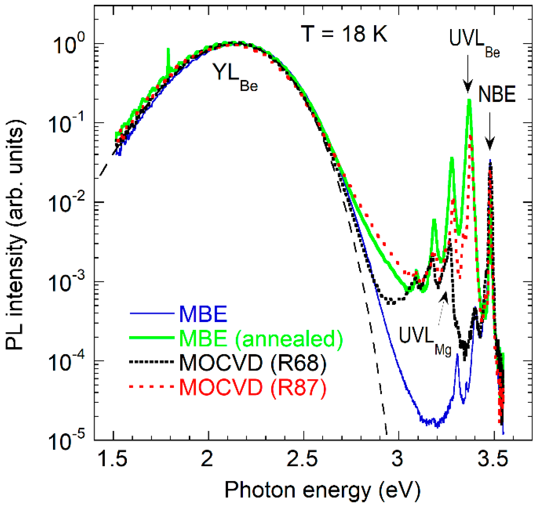
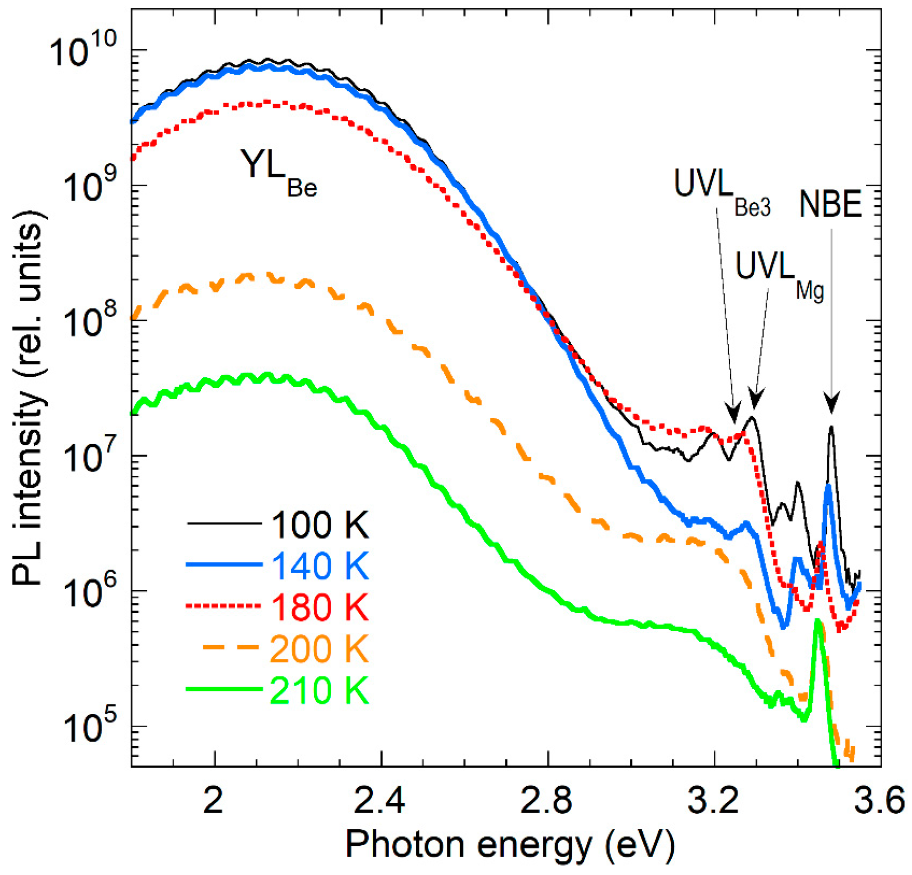
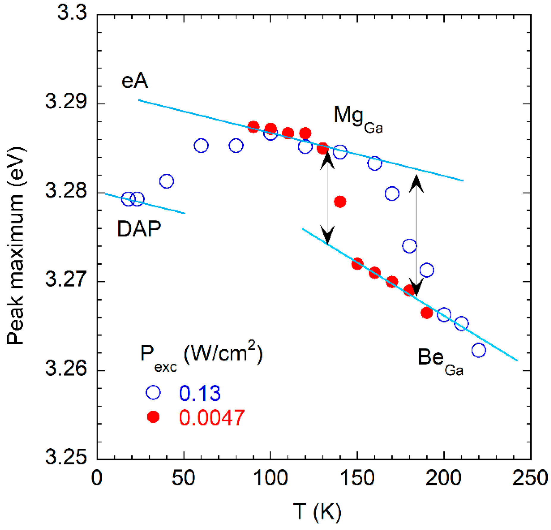
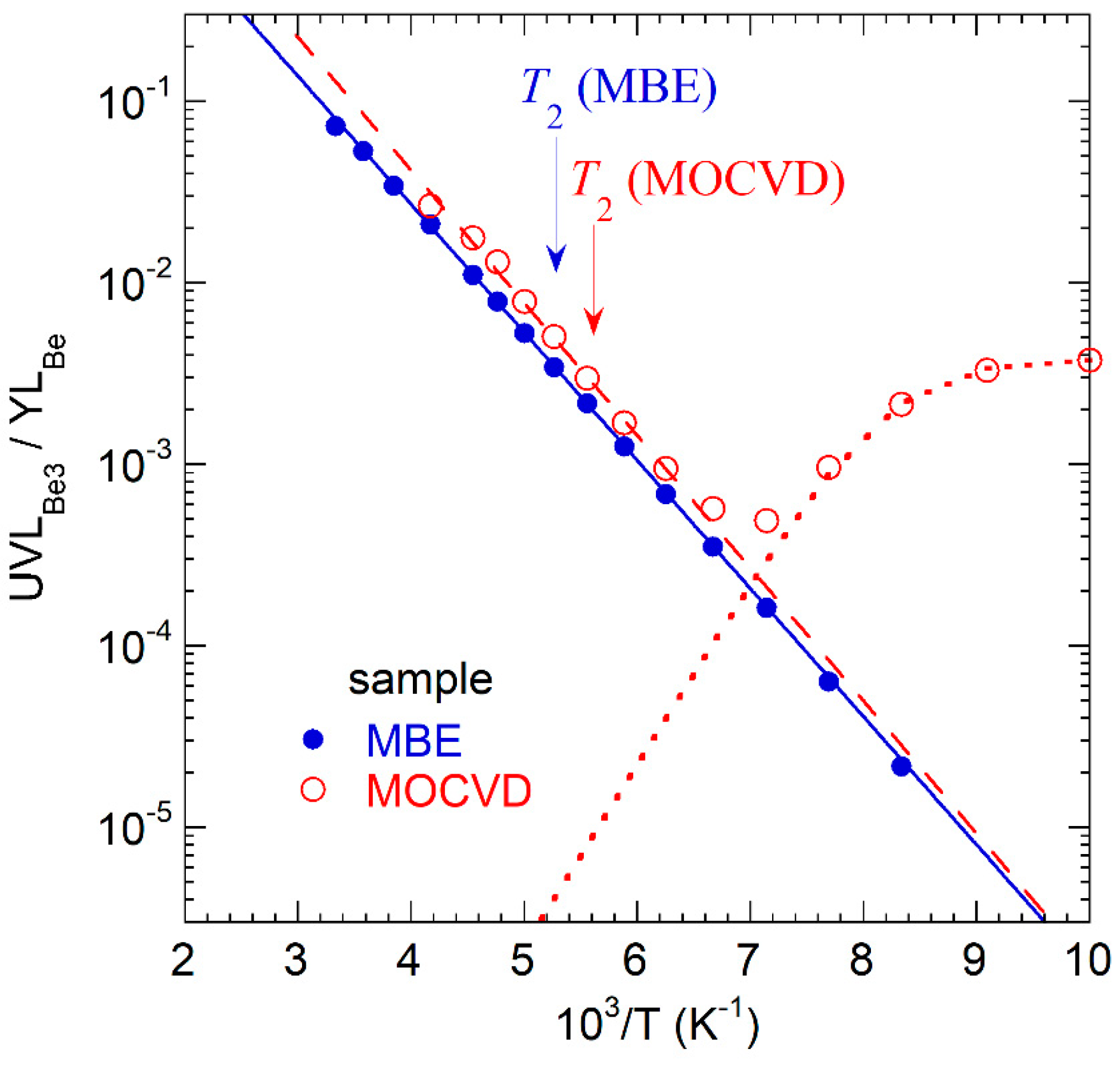
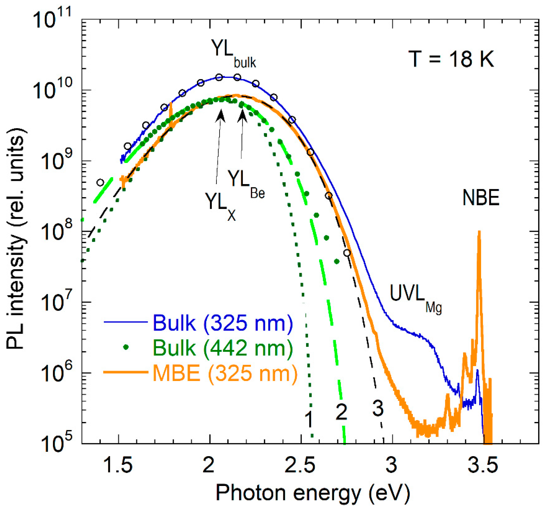
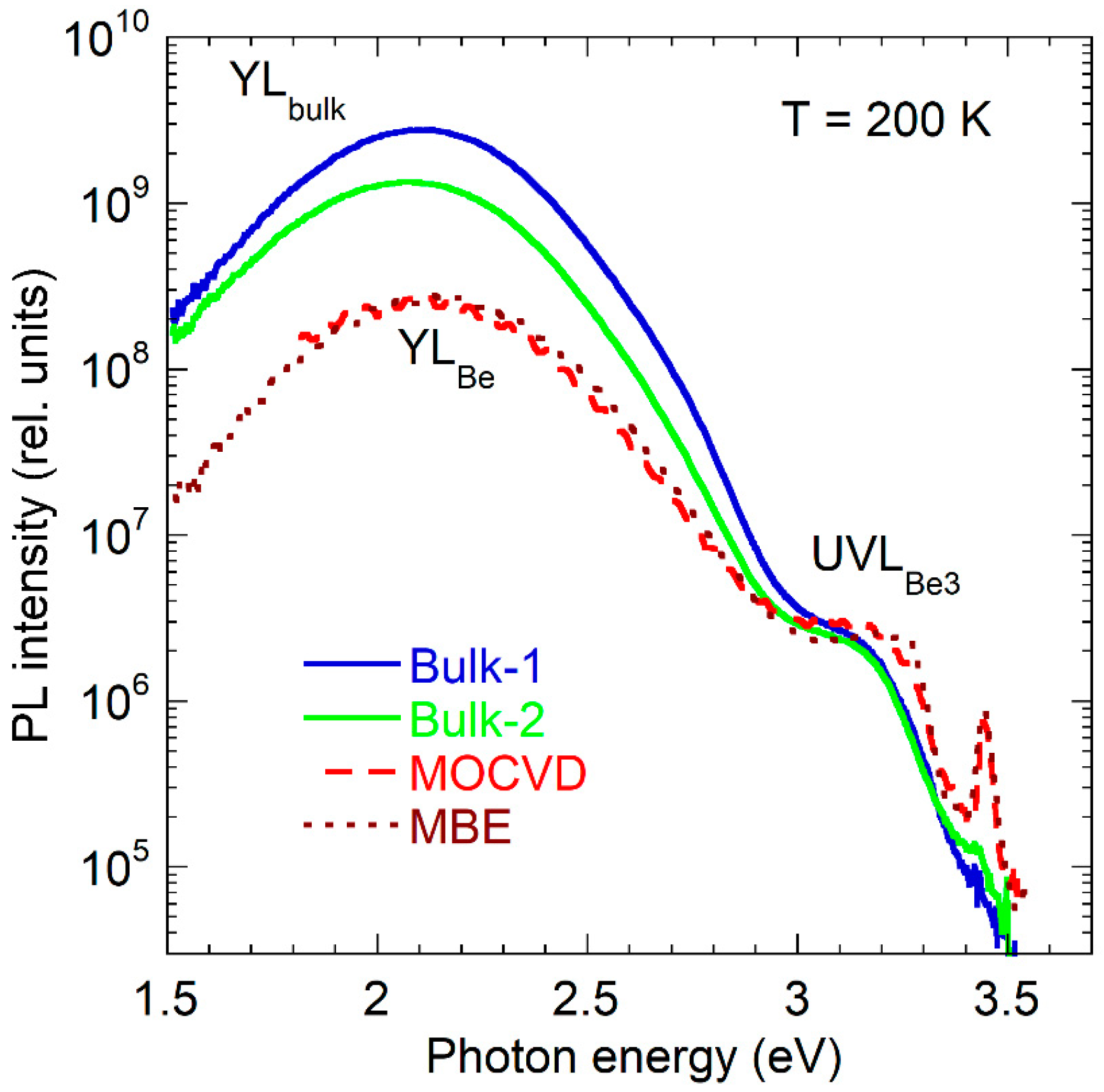
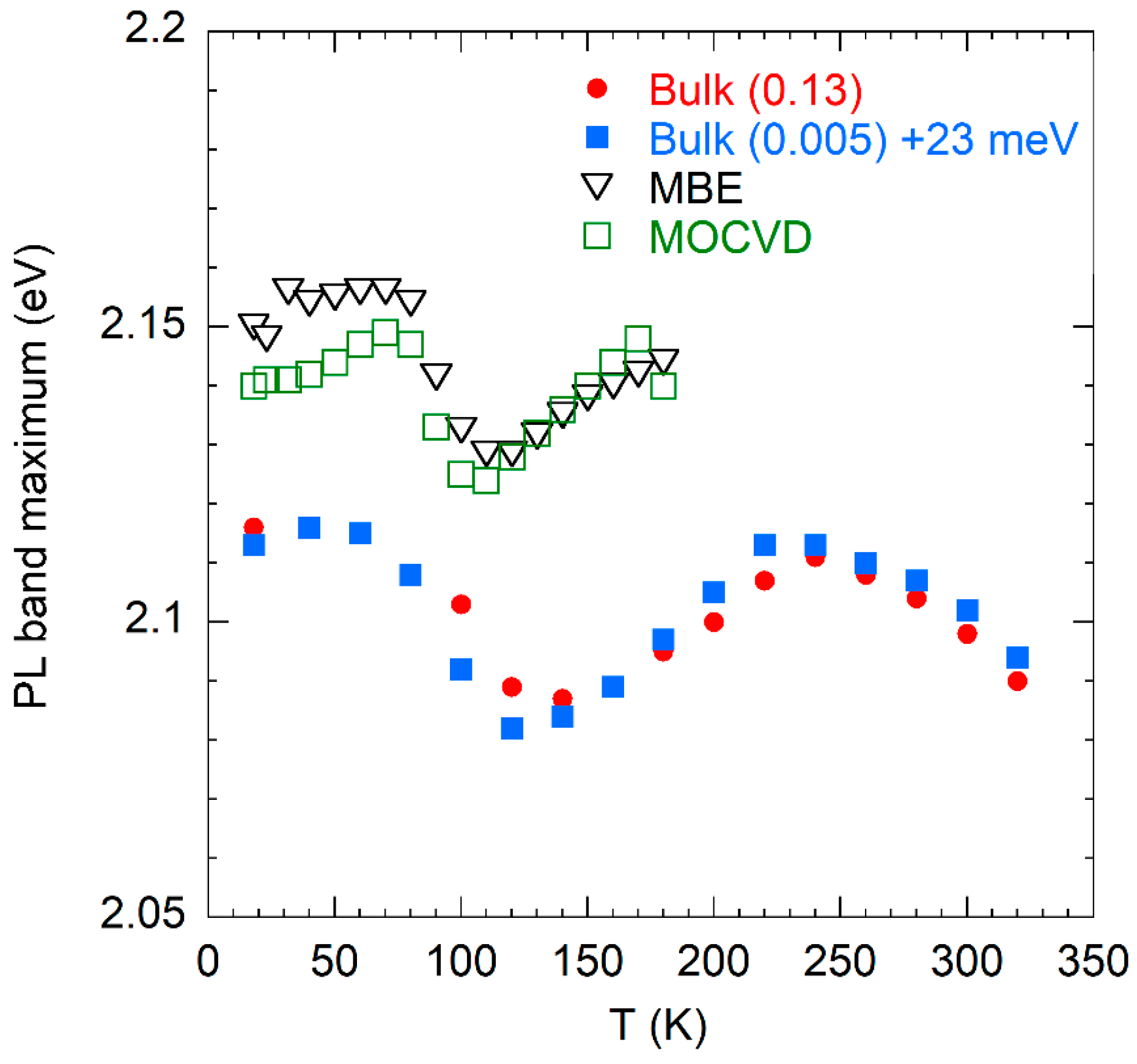
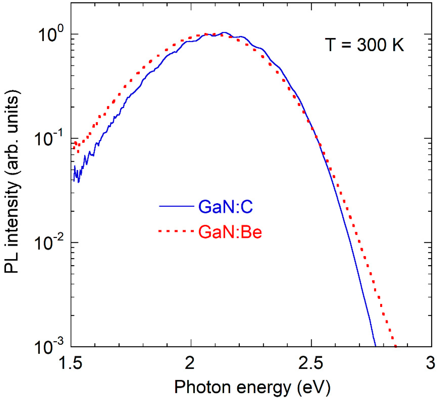
3.1. PL Bands in Be-Doped GaN Grown by MOCVD and MBE Techniques

The shape and position of the YLBe band are well reproduced in many GaN layers grown by MOCVD and MBE. Figure 1 shows representative PL spectra at T = 18 K. The shape of the YLBe band can be fitted (the dashed line) with the following expression obtained in the one-dimensional configuration coordinate model [37]:
I P L ( ω ) = I P L ( ω max ) exp 2 S e E 0 * ω + Δ d F C g 1 2 .
Here, Se is the Huang–Rhys factor in the excited state of the defect; dFCg = E 0 * ħωmax is the Frank–Condon shift in the ground state; E 0 * = E0 + 0.5ħΩe, where E0 is the ZPL energy and ħΩe is the energy of the effective phonon mode in the excited state; and ħω and ħωmax are the photon energy and position of the PL band maximum, respectively. The Δ is a minor shift of the PL band maximum due to sample-dependent reasons such as in-plane biaxial strain in thin GaN layers grown on sapphire substrates (blue shift) or local electric fields (red shift).
In addition to the YLBe band, PL spectra from Be-doped GaN grown by MOCVD and MBE contain two UVL bands: the MgGa-related UVLMg band, with the first peak at 3.27 eV, and the Be-related UVLBe band, with the first peak at 3.38 eV. Both peaks are followed by a few LO phonon replicas. The UVLMg band is caused by mild contamination with Mg during growth (especially significant in our MOCVD GaN:Be samples). The UVLBe band was found in the majority of GaN:Be samples. In MBE-grown samples, it required activation by annealing at T > 750 °C (Figure 1). Our earlier attribution of this band to the shallow state of the BeGa acceptor [20] was later rejected, and the band is preliminary attributed to a complex defect involving Be [25].
The best way to recognize the BeGa-related YLBe band is to investigate the temperature evolution of the PL spectrum, the characteristic features of which were reproduced in all studied GaN:Be samples grown by MBE and MOCVD [25]. The YLBe band is quenched in two steps. At T ≈ 100 K, the YLBe band intensity drops (usually by a factor of about 2) and the band abruptly redshifts by up to 50 meV. This behavior is explained by the relaxation of the bound hole from the polaronic state Be1 at 0.33 eV to the polaronic state Be2 at 0.38 eV. At T > 180 K, the second quenching is observed (Figure 2). In conductive n-type GaN:Be samples, the second quenching reveals an activation energy of 0.30 eV, while in semi-insulating samples, the quenching occurs by the abrupt and tunable quenching (ATQ) mechanism [38].
The most important feature of the temperature evolution of PL is the emergence of a UVL band (UVLBe3) at T > 140 K (Figure 2). The shift of the UVL maximum with temperature is shown in Figure 3. At T < 25 K, the UVL band is caused by donor-acceptor-pair (DAP)-type transitions of electrons from shallow ON donors to shallow MgGa acceptors. At T > 50 K, the DAP peaks are replaced with similar peaks caused by electron transitions from the conduction band to the MgGa acceptors (eA transitions). At T > 130 K, the UVLMg band is quenched by the ATQ mechanism. A similar in shape but slightly red-shifted UVLBe3 band emerges at higher temperatures. It can be seen from Figure 3 that the ZPL of the UVLBe3 is red-shifted by 13 ± 3 meV from the ZPL of the UVLMg band. Since the transition level of the shallow MgGa acceptor is located at 223 ± 3 meV above the VBM at T = 18 K [12], we conclude that the shallow −/0 transition level of the BeGa acceptor (the Be3 state) is located at 236 ± 5 meV above the VBM. With increasing temperature, the Be3 level moves towards the valence band (0.20 eV at T ≈ 200 K) [25].
In agreement with the model proposed in Ref. [25], the ratio UVLBe3/YLBe of PL intensities is the same in all GaN:Be samples. This ratio is described in a wide range of temperatures with Equation (1), where ΔE is the energy distance between the Be2 and Be3 states (ΔE = 140–145 meV). Figure 4 shows the dependence for two samples. In the MOCVD GaN:Be sample, the UVLMg band is quenched and replaced by the UVLBe3 band at T > 140 K (compare Figure 3 and Figure 4 for this sample).
A remarkable feature of this model is that the second step of the YLBe quenching is caused by the thermal emission of holes, not from a deep but from the shallow Be3 level, to the valence band. In particular, the activation energy of 0.30 eV obtained from this quenching in conductive n-type GaN:Be samples is the sum of the Be3 ionization energy and ΔE [25]. From this, the deepest polaronic state of the BeGa acceptor is found at 0.38 ± 0.03 eV above the VBM in the limit of low temperatures (≈0.30 eV at T = 200 K). The unique interplay of the UVLBe3 and YLBe bands will be used below to recognize the YLBe band in bulk GaN crystals.

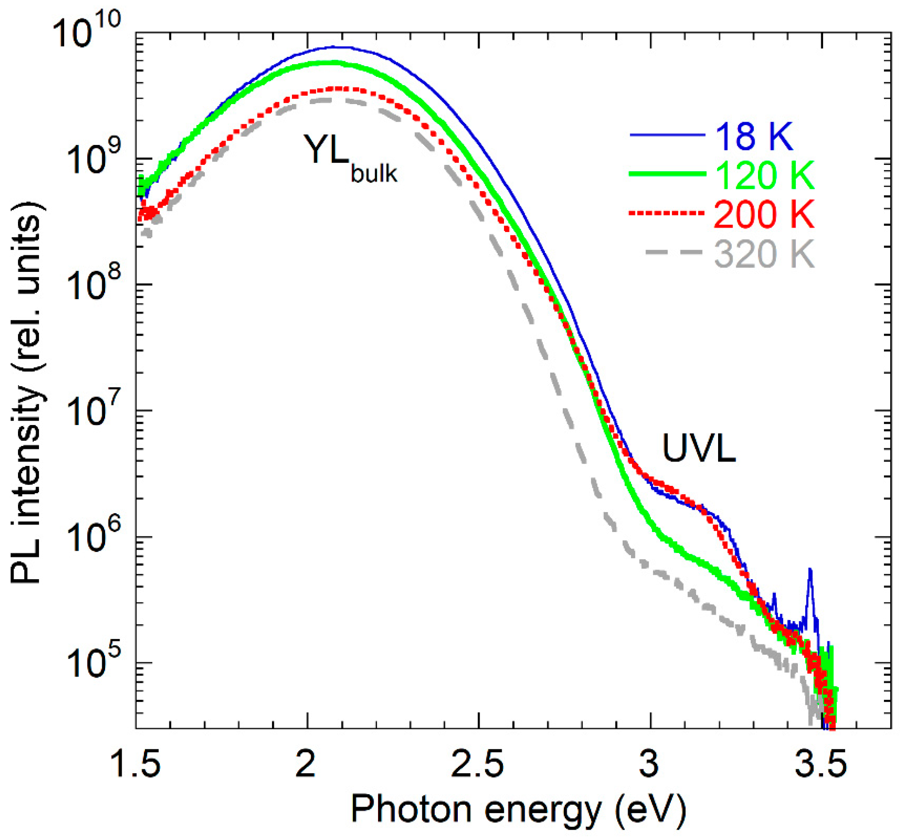
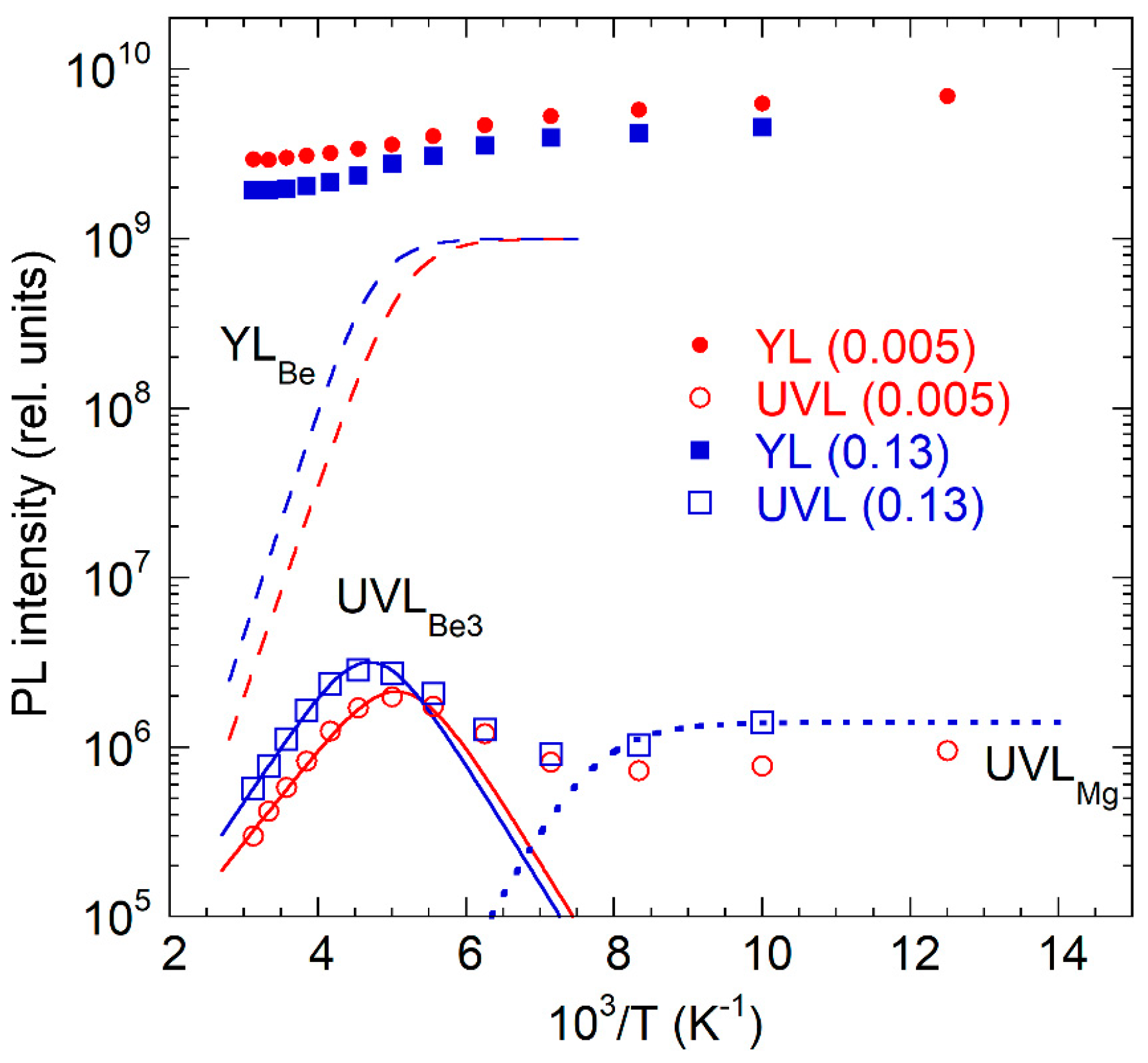
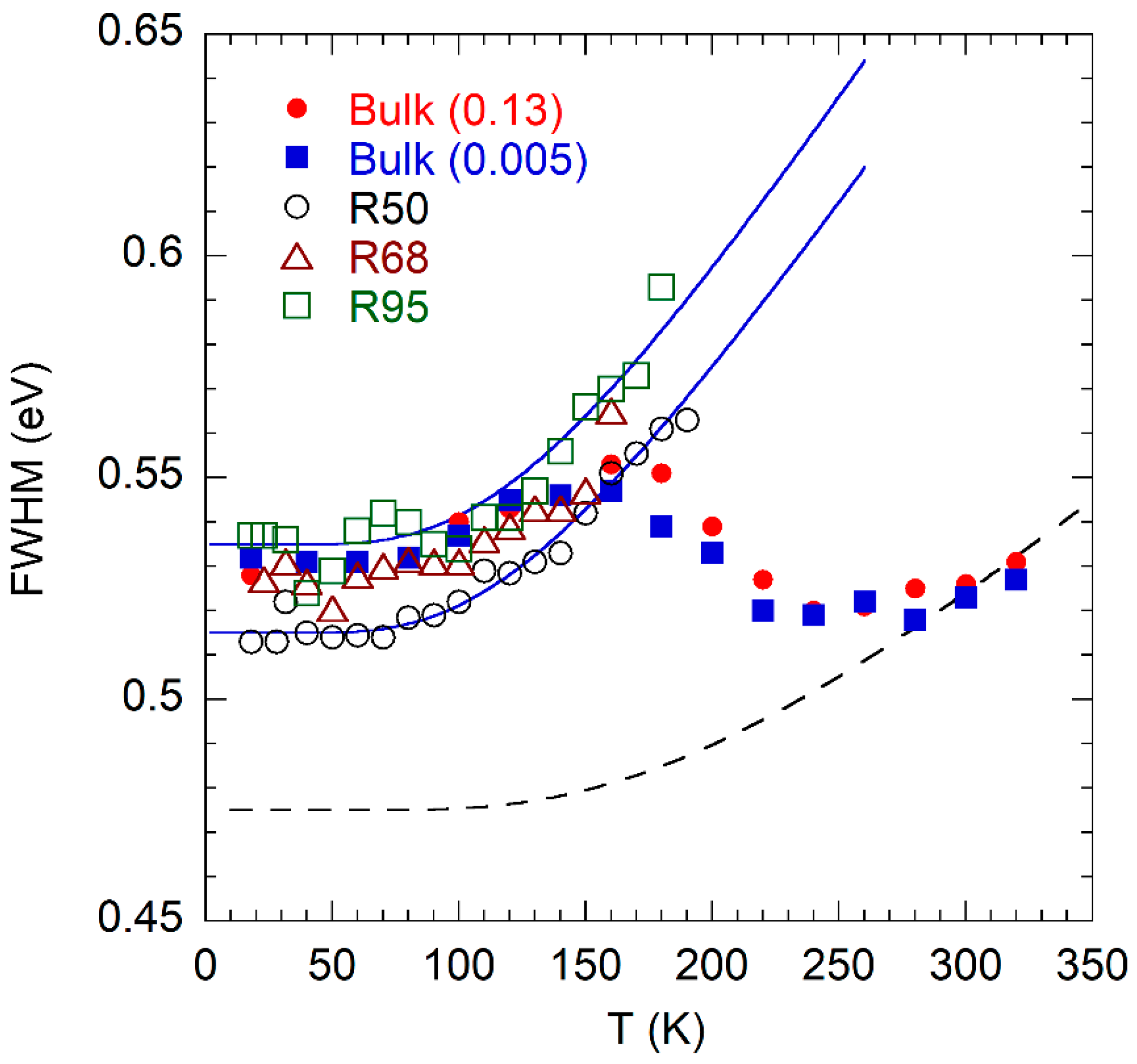
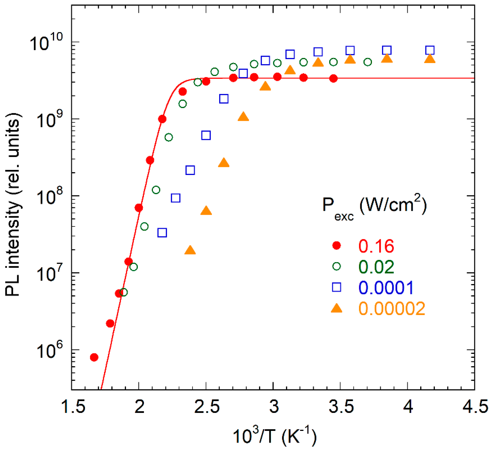
3.2. The Yellow Band in Bulk GaN:Be Grown by High-Pressure Technique

Figure 5 shows PL spectra from bulk GaN:Be excited above-bandgap (with the 325 nm line of the HeCd laser at 3.81 eV) and below-bandgap (with the 442 nm line of the HeCd laser at 2.80 eV). The spectra are compared with the PL spectrum from MBE-grown GaN:Be. In the case of the usual above-bandgap excitation, a very weak near-band-edge (NBE) emission is detected at 3.47 eV. The UVLMg band appears as a structureless shoulder at about 3.2 eV. We assume that its ZPL and LO phonon replicas are unresolved because of strong local electric fields caused by short-range potential fluctuations in heavily doped and compensated GaN:Be [39].
The yellow band (YLbulk) at ~2.1 eV is broad and very strong, in agreement with earlier reports [28,29]. With increasing excitation intensity, Pexc, from 10−5 to ~100 W/cm2, it blueshifts by about 0.1 eV. After a laser pulse at T = 18 K, the PL intensity decays nonexponentially, approximately as t−1.2 at time delays t between 1 and 1000 s, and the band redshifts by almost 0.1 eV. Such behavior agrees with the presence of potential fluctuations.
The yellow band in bulk GaN:Be crystals can also be excited below the bandgap. The spectrum obtained after excitation with the 442 nm line of the HeCd laser (2.8 eV) is shown in Figure 5 with filled circles. This band (temporarily labeled YLX) is also broad and its maximum is at 2.07 eV. Interestingly, the sum of the YLBe band in MBE GaN:Be and the YLX band matches the shape of the YLbulk band observed after the above-bandgap excitation (Figure 5). This is the first indication that the YLbulk band may consist of two unresolved broad bands, one of which is the well-studied BeGa-related YLBe band. A stronger argument follows from the analysis of the evolution of the PL spectrum with temperature, as discussed below.
Figure 6 shows the PL spectrum from bulk GaN:Be at selected temperatures. The intensity of the YLbulk band changes insignificantly with increasing temperature from 18 to 320 K. The intensity of the UVL band decreases between 18 and 140 K and then increases (between 140 and 200 K). While the fine structure of the UVL band cannot be resolved, the increase in the UVL intensity is very similar to that observed in the GaN:Be samples grown by MBE and MOCVD [25].
Figure 7 compares PL spectra at T = 200 K for bulk GaN:Be (at two crystal locations) and GaN:Be layers grown by MBE and MOCVD (arbitrarily shifted vertically to match the UVL intensity). The ratio of intensities UVLBe3/YLBe at the selected temperature must be the same in all Be-doped GaN samples. Assuming that the UVLBe3 band emerges with the temperature [25], we conclude that the YLBe band in bulk GaN is hidden under a stronger yellow band of different origin (YLX).
Figure 8 shows an Arrhenius plot for the studied PL bands in bulk GaN:Be. The expected temperature dependence of the MgGa-related UVLMg intensity is shown with a dotted line. The temperature dependences for the BeGa-related YLBe band (shown with dashed lines) are simulated to fit the UVLBe3 dependences by fixing the UVLBe3/YLBe ratio according to Equation (1) with earlier-found parameters.
The first step of the YLBe quenching is expected at T ≈ 100 K but cannot be resolved. The YLBe band hides under a stronger yellow band at T < 200 K and completely disappears at temperatures approaching room temperature, as expected [25]. We estimate that the YLX band is stronger than the YLBe band by a factor of 2–5 at T < 200 K.
We also studied the temperature dependence of the YLbulk full width at half maximum (FWHM or W) and compared it with that for the YLBe band in the GaN:Be samples grown by MOCVD (Figure 9). For PL bands that are broad due to strong electron–phonon coupling, the W(T) dependence can be fitted with the following expression [6]:
W ( T ) = W ( 0 ) coth ( Ω e 2 k T ) ,
where ħΩe is the energy of the effective phonon mode. For MOCVD-grown GaN:Be samples, the fit with ħΩe = 38 meV is relatively good, and the value of the single fitting parameter is typical for defects in GaN (between 23 and 56 meV) [37,40,41]. However, the W(T) dependence for the YLbulk band in bulk GaN:Mg shows abnormal narrowing with increasing temperature from ~170 to 250 K. This temperature region roughly corresponds to the region where the YLBe band is quenched. We conclude that at T > 250 K, the contribution of the YLBe band to the YLbulk band can be ignored and only the YLX band remains. The FWHM of the YLX band is smaller than that of the YLBe band, while the parameter ħΩe is larger (Figure 9).
Figure 10 shows the temperature dependence of the YLbulk band maximum (shifted up by 23 meV for Pexc = 0.005 W/cm2) in comparison with the dependence for the YLBe band in the MOCVD and MBE GaN:Be samples. The sudden shift at about 100 K is similar in all the samples, and it can be explained by replacing the YLBe1 with the YLBe2, PL bands associated with two deep polaronic states of the BeGa acceptor [25]. At T > 230 K, the band maximum corresponds to the YLX band because the YLBe band is quenched. Note that the YLbulk band shifts significantly with excitation intensity (up to 0.1 eV with a variation of Pexc from 10−5 to ~100 W/cm2), whereas the shift of the YLBe band in the MOCVD and MBE GaN:Be samples is insignificant.
To further explore the properties of the YLX band, we conducted PL experiments by using a high-temperature cryostat (Figure 11). The YLX band is quenched by the ATQ mechanism, which is typical for defects in semi-insulating GaN [38]. Formally, it can be described with the commonly used expression:
I P L ( T ) = I P L ( 0 ) 1 + C exp E A k T
However, unlike the PL quenching in conductive n-type GaN, the parameter EA does not have a physical meaning [17]. The quenching is very abrupt, yet the slope of the quenching could be smoothened by potential fluctuations [42], or other reasons [38]. The quenching is tunable by excitation intensity.

4. Discussion

The results of this study indicate that at least two PL bands contribute to the YLbulk band, with a maximum at about 2.1 eV in bulk GaN:Be grown by the HNPS method. These are the YLBe band (with a maximum at 2.15 eV) associated with the isolated BeGa acceptor and the YLX band (at ~2.06 eV) caused by a different defect. Since the YLBe band is well studied [25], we will focus below on the analysis of the YLX band, which is the strongest PL band at all studied temperatures.

4.1. Type of Transition

The YLX band at T = 18 K can be excited below-bandgap, with photon energies of 2.8 eV (Figure 5). Earlier, the onset of the PL excitation (PLE) spectrum of the yellow band was found at 2.8 eV at 7 K, and the YLbulk band could be excited with a 2.78 eV laser [28]. At room temperature (when we expect only the YLX band), the PLE spectrum also shows an onset at about 2.7–2.8 eV [29]. We assume that the YLX band is caused by electron transitions from the conduction band (or from shallow donors) to a deep defect level, as it occurs for almost all defects in GaN [7,17]. Then, the results of the current work and those of previous studies indicate that the related defect level is located no closer than 0.8 eV to the VBM. Nonexponential and slow PL decay after a laser pulse agrees with the assumed type of transition. This PL cannot be caused by transitions from an excited state to the ground state of some defect because such transitions are characterized by exponential PL decay, even at very low temperatures, and positions of such PL bands are not affected by local electric fields [7,17]. At this point, transitions from a deep donor to an acceptor (or a deeper donor) cannot be excluded since such transitions are possible in heavily doped GaN and are characterized by slow, nonexponential decay. If this was the case, the defect level responsible for the YLX band would be much closer to the VBM than 0.8 eV. However, the quenching of the YLX band at T > 450 K (Figure 11 and the data in Ref. [28]) favors the assumption that the related defect level is at 0.8–0.9 eV above the VBM. It was shown in Ref. [17] that for defects with relatively strong PL in GaN, the quenching begins at T = 400–500 K (at Pexc ≈ 0.1 W/cm2 when the quenching occurs by the ATQ mechanism) if the defect level is located at 0.6–1.0 eV above the VBM. Transitions from the conduction band (or from shallow donors) to a defect level at ~0.8 eV above the VBM may be characterized by a nonexponential, slow decay of PL and by relatively large PL band shifts with a variation of Pexc if local electric fields (e.g., due to potential fluctuations) are present. ODMR and photo-EPR studies of the yellow band in similar bulk GaN:Be crystals support this type of transition [33,35]. We exclude the possibility of electron transitions from a defect level located in the upper part of the gap to the valence band as the origin of the YLX band. Such transitions cannot be observed because photogenerated holes are captured by various acceptors with the multiphonon nonradiative mechanism many orders of magnitude faster than via radiative transitions [7].

4.2. On Identification of the YLX Band in Bulk GaN

The observed broad YLbulk band in bulk GaN:Be consists of at least two unresolved bands, one of which is a well-studied YLBe band associated with the isolated BeGa acceptor. Another PL band (temporarily labeled YLX) is caused by electron transitions from the conduction band (or shallow donors) to a deep defect (donor or acceptor), with a transition level at 0.8–0.9 eV above the VBM. Since the main difference between GaN:Be layers grown by MBE or MOCVD methods and bulk GaN:Be crystals grown by the HNPS method is a high concentration of oxygen in the latter, it is tempting to attribute it to the BeGaON complex, which is expected to be a deep donor [27]. However, the first-principles calculations using the Heyd–Scuseria–Ernzerhof (HSE) hybrid functional [43] predict that the 0/+ level of the BeGaON defect is located at 0.26 eV above the VBM [27], or that this defect has no transition levels in the bandgap [23]. Whereas fair agreement of theoretical predictions with experimental findings is observed for the BeGa acceptor, the disagreement for the 0/+ level of the BeGaON defect is significant (Table 1).
Another possibility is that the YLX band is the CN-related YL1 band slightly broadened and redshifted because of potential fluctuations (Figure 12). Both PL bands are quenched at T > 500 K in semi-insulating GaN (at Pexc ≈ 0.1 W/cm2). The concentration of carbon impurities in the studied bulk GaN:Be samples is about 5 × 1017 cm−3, which is enough to cause a strong yellow band.
Below, we will discuss two candidates for the YLX band (CN acceptor and BeGaON donor). Parameters of defects that may contribute to the YLbulk band are given in Table 2. The hole-capture coefficient, Cp, for the CN acceptor is (3.7 ± 1.6) × 10−7 cm3/s. The Cp for the BeGa acceptor was estimated from the YLBe quenching as 4 × 10⁻⁷ cm3/s. However, careful analysis of PL quenching in numerous MOCVD GaN:Be samples (which contain C and Be, with concentrations of about 1017 cm−3 and (1–30) × 1017 cm−3, respectively) shows that the Cp for the BeGa acceptor is larger, which is consistent with the capture of holes by a shallow acceptor level located at 0.2 eV above the VBM. It was shown in Ref. [25] that Cp = 10−6 cm3/s agrees with the experimental data. Note that for another shallow acceptor (MgGa), Cp is also 10−6 cm3/s. We will consider this value hereafter for the BeGa acceptor that captures holes at its shallow level at 0.2 eV above the VBM [25]. The Cp for the BeGaON complex is expected to be significantly smaller because of the donor nature of this defect. The Cp for donors in GaN varies from 10−10 to 4 × 10⁻⁸ cm3/s [17]. At low enough temperatures (before the PL quenching begins), the PL intensity from defects in GaN (both conductive n-type and semi-insulating) is proportional to the concentration of defects and their hole-capture coefficient, i.e., IiPL = ACpiNi for defect i, where A is a constant. From the experiment, IXPL/IBePL = 2–5.

4.2.1. Can the YLX Band Be the CN-Related YL1 Band?

In the first scenario, the intensity of the YL1 band at T ≈ 100 K is about 2–5 times higher than that of the YLBe band, and the contribution of PL from the BeGaON complex is negligible. For this, the concentration of isolated BeGa defects should be about 1017 cm−3. Then, ICPL/IBePL = Cp,CNC/Cp,BeNBe = 4 if we use the corresponding parameters in Table 2. Such a low concentration of isolated BeGa defects (by a factor of 30 lower than the total concentration of Be atoms) implies that the concentration of BeGaON complexes may reach 3 × 1019 cm−3, i.e., the majority of Be atoms form complexes with oxygen. The concentration of ON donors may not exceed the total concentration of acceptors (CN and BeGa) because the samples are semi-insulating and the BeGaON donors are neutral. Such a high concentration of BeGaON would not contribute to PL if the hole-capture coefficient for this donor is low (IBeOPL/IBePL = Cp,BeONBeO/Cp,BeNBe = 0.3 if Cp for the BeGaON complex is 10−9 cm3/s) or if the BeGaON is not participating in electron–hole recombination as it was predicted in Ref. [23].

4.2.2. Can the YLX Band Be Caused by the BeGaON Complex?

In the second scenario, the intensity of the assumed YLBeO band from the BeGaON complex at T ≈ 100 K is about 2–5 times higher than that of the YLBe band, and the YL1 band from the CN acceptors is negligibly weak. For this, the concentration of isolated BeGa defects should be at least 1018 cm−3 (so that ICPL/IBePL = Cp,CNC/Cp,BeNBe < 0.4), and the Cp for the BeGaON donor should be relatively high (so that IBeOPL/IBePL = Cp,BeONBeO/Cp,BeNBe = 2–5). This scenario would work if NBeO = 3 × 1019 cm−3 and Cp,BeO = 10−7 cm3/s (Table 2). The main argument against this scenario is a conflict between the predicted ionization energy of the BeGaON (0.26 eV or no level) [23,27] and the experimentally found transition level at 0.8–0.9 eV. However, a strong argument favoring this scenario was a good agreement between theoretical predictions and experiments in PL under hydrostatic pressure [27]. Below, we will suggest an alternative interpretation of these experiments.

4.3. Interpretation of Other Experiments

Exciting results were obtained in Ref. [27], where PL from bulk GaN:Be was studied at T = 10 K under hydrostatic pressure, p, up to 12.5 GPa. With increasing p, the YL band splits into two components: component A blue-shifts with a moderate rate (20 meV/GPa, similar to the typical shift of the CN-related YL1 band), while component B blue-shifts much faster (about 90 meV/GPa). Component A was attributed to the CN acceptor, while components B and C were related to the deep (polaronic) and shallow (delocalized) states of the BeGaON complex. A remarkable result is that at p > 8 GPa, component C emerges at about 3.6 eV and becomes the strongest PL band at p > 9 GPa. This unusual phenomenon was explained by the dual nature of the BeGaON defect: namely, the deeper state with a highly localized hole (calculated 0/+ level at 0.26 eV above the VBM at p = 0) moves towards the VBM with hydrostatic pressure. At p = 8 GPa, a shallow state of this defect (the 0/+ level at 0.12 eV above the VBM) with a delocalized hole becomes the most stable configuration. At pressures between 9 and 12.5 GPa, both PL signals are observed: a relatively narrow PL band close to the bandgap, which is caused by electron transitions from the conduction band to the shallow level, and a broad band at about 3 eV, which is caused by electron transitions from the conduction band to the deep state of the BeGaON defect. The calculated barrier between the shallow and deep states is 0.24 eV [27]. The same calculations predict that the polaronic state of the isolated BeGa defect is deeper (0.55 eV above the VBM), and the deep states of the BeGa and BeGaON defects shift similarly with hydrostatic pressure [27].
We agree that component A of the yellow band can be the YL1 band caused by the CN acceptor but suggest that component B is caused by the isolated BeGa defect (the −/0 transition level at 0.38 eV above the VBM and the PL band maximum at 2.15 eV). With increasing p, this level shifts towards the valence band and, at p ≈ 8 GPa, intersects the shallow level of the BeGa (at 0.24 eV above the VBM at p = 0). At higher pressures, the UVLBe3 band of the BeGa acceptor emerges even at T = 10 K because this configuration becomes the most stable. It may be interesting to test the above explanation by investigating MOCVD GaN:Be samples under hydrostatic pressure. As for the BeGaON complexes, we expect that they are either nonradiative, weakly radiative, or “inert” defects, so that their contribution to PL can be ignored even if their concentration is about 3 × 1019 cm−3.
Our interpretation of the PL results is consistent with the results of photo-EPR studies on similar bulk Be-doped GaN crystals [35,36]. Willoughby et al. [35] initially attributed the photo-EPR signal from Be-doped GaN crystals to a Be-related acceptor, with the −/0 transition level at 0.7 eV above the VBM. However, these authors later revised their attribution and explained this photo-EPR signal by recombination of electrons with holes bound to the CN acceptor [36]. Note that slow transients of the photo-EPR signal, explained by trapping electrons by a Be-related defect level close to the conduction band [36], could be caused by potential fluctuations and local electric fields. This is also consistent with the very slow PL decays for the YLbulk band [28]. The attribution of the YLbulk band to a superposition of the YLBe and YL1 bands may also explain the results obtained by Glaser et al. [33]. They observed ODMR signals from bulk GaN:Be crystals grown by the HNPS method (with a carbon concentration of 1017 cm−3) and noted that the g-values for the yellow band in these samples were very close to those for the YL band in undoped GaN (i.e., for the CN-related YL1 band).

5. Conclusions

The broad yellow luminescence band in bulk GaN crystals grown by high-pressure technique and doped with Be consists of two unresolved bands: the BeGa-related YLBe band and the YLX band, which is most likely the CN-related YL1 band. At T > 200 K, the YLBe band is quenched, while the quenching of the YLX band begins only at 400–500 K. We conclude that the yellow band, previously attributed to the BeGaON complex based on first-principles calculations and PL experiments with hydrostatic pressure [27], is in fact the BeGa-related YLBe band, whereas the BeGaON defect is either optically inactive or its contribution to PL is negligible. At the same time, the concentration of the BeGaON complexes in these bulk GaN crystals significantly exceeds the concentration of the isolated BeGa defects.

Author Contributions

Conceptualization, M.A.R. and M.B.; methodology, M.A.R. and M.B.; software, M.A.R.; validation, M.A.R. and M.B.; formal analysis, M.A.R.; investigation, M.A.R. and M.B.; resources, M.A.R. and M.B.; data curation, M.A.R.; writing—original draft preparation, M.A.R.; writing—review and editing, M.A.R. and M.B.; visualization, M.A.R.; supervision, M.A.R.; project administration, M.A.R.; funding acquisition, M.A.R. and M.B. All authors have read and agreed to the published version of the manuscript.

Funding

This research at VCU was funded by the National Science Foundation, grant number DMR-1904861. The work at IHPP was supported by the Polish National Centre for Research and Development through project TECHMATSTRATEG-III/0003/2019-00.

Data Availability Statement

Data are contained within the article.

Conflicts of Interest

The authors declare no conflict of interest.

References

  1. Morkoç, H. Handbook of Nitride Semiconductors and Devices; Wiley: New York, NY, USA, 2008. [Google Scholar]
  2. Pearton, S.J.; Zolper, J.C.; Shul, R.J.; Ren, F. GaN: Processing, defects, and devices. J. Appl. Phys. 1999, 86, 1–78. [Google Scholar] [CrossRef]
  3. Li, G.; Wang, W.; Yang, W.; Lin, Y.; Wang, H.; Lin, Z.; Zhou, S. GaN-based light-emitting diodes on various substrates: A critical review. Rep. Prog. Phys. 2016, 79, 056501. [Google Scholar] [CrossRef] [PubMed]
  4. Jones, E.A.; Wang, F.; Costinett, D. Review of Commercial GaN Power Devices and GaN-Based Converter Design Challenges. IEEE J. Emerg. Sel. Top. Electron. 2016, 4, 707–719. [Google Scholar] [CrossRef]
  5. Dean, P.J. Photoluminescence as a diagnostic of semiconductors. Prog. Cryst. Growth Charact. 1982, 5, 89–174. [Google Scholar] [CrossRef]
  6. Reshchikov, M.A.; Morkoç, H. Luminescence properties of defects in GaN. J. Appl. Phys. 2005, 97, 061301. [Google Scholar] [CrossRef]
  7. Reshchikov, M.A. Measurement and analysis of photoluminescence in GaN. J. Appl. Phys. 2021, 129, 121101. [Google Scholar] [CrossRef]
  8. Ogino, T.; Aoki, M. Mechanism of Yellow Luminescence in GaN. Jpn. J. Appl. Phys. 1980, 19, 2395–2405. [Google Scholar] [CrossRef]
  9. Pankove, J.I.; Hutchby, J.A. Photoluminescence of ion-implanted GaN. J. Appl. Phys. 1976, 47, 5387–5390. [Google Scholar] [CrossRef]
  10. Reshchikov, M.A. On the Origin of the Yellow Luminescence Band in GaN. Phys. Stat. Sol. (b) 2023, 260, 2200488. [Google Scholar] [CrossRef]
  11. Lyons, J.L.; Janotti, A.; Van de Walle, C.G. Carbon impurities and the yellow luminescence in GaN. J. Appl. Phys. 2010, 97, 152108. [Google Scholar] [CrossRef]
  12. Reshchikov, M.A.; McNamara, J.D.; Zhang, F.; Monavarian, M.; Usikov, A.; Helava, H.; Makarov, Y.; Morkoç, H. Zero-phonon line and fine structure of the yellow luminescence band in GaN. Phys. Rev. B 2016, 94, 035201. [Google Scholar] [CrossRef]
  13. Reshchikov, M.A.; Vorobiov, M.; Demchenko, D.O.; Özgür, Ü.; Morkoç, H.; Lesnik, A.; Hoffmann, M.P.; Hörich, F.; Dadgar, A.; Strittmatter, A. Two charge states of the CN acceptor in GaN: Evidence from photoluminescence. Phys. Rev. B 2018, 98, 125207. [Google Scholar] [CrossRef]
  14. Zimmermann, F.; Beyer, J.; Röder, C.; Beyer, C.; Richter, E.; Irmscher, K.; Heitmann, J. Current Status of Carbon-Related Defect Luminescence in GaN. Phys. Stat. Sol. (a) 2021, 218, 2100235. [Google Scholar] [CrossRef]
  15. Suski, T.; Perlin, P.; Teisseyre, H.; Leszczynski, M.; Grzegory, I.; Jun, J.; Boćkowski, M.; Porowski, S. Mechanism of yellow luminescence in GaN. Appl. Phys. Lett. 1995, 67, 2188–2190. [Google Scholar] [CrossRef]
  16. Reshchikov, M.A.; Usikov, A.; Helava, H.; Makarov, Y.; Prozheeva, V.; Makkonen, I.; Tuomisto, F.; Leach, J.H.; Udwary, K. Evaluation of the concentration of point defects in GaN. Sci. Rep. 2017, 7, 9297. [Google Scholar] [CrossRef] [PubMed]
  17. Reshchikov, M.A. Photoluminescence from defects in GaN. In Proceedings of SPIE 12421, Gallium Nitride Materials and Devices XVIII; Fujioka, H., Morkoç, H., Schwarz, U., Eds.; SPIE: San Francisco, CA, USA, 2023; p. 1242109. [Google Scholar]
  18. Ilegems, M.; Dingle, R. Luminescence of Be- and Mg-doped GaN. J. Appl. Phys. 1973, 44, 4234–4235. [Google Scholar] [CrossRef]
  19. Chen, L.; Skromme, B. Spectroscopic Characterization of Ion-Implanted GaN. In GaN and Related Alloys—2002; Materials Research Society Symposium—Proceedings; Wetzel, C., Yu, E.T., Speck, J.S., Rizzi, A., Arakawa, Y., Eds.; Cambridge University Press: Boston, MA, USA, 2003; Volume 743, pp. 755–760. [Google Scholar]
  20. Demchenko, D.O.; Vorobiov, M.; Andrieiev, O.; Myers, T.H.; Reshchikov, M.A. Shallow and deep states of beryllium acceptor in GaN: Why photoluminescence experiments do not reveal small polarons for defects in semiconductors. Phys. Rev. Lett. 2021, 126, 027401. [Google Scholar] [CrossRef]
  21. Ahmad, H.; Lindemuth, J.; Engel, Z.; Matthews, C.M.; McCrone, T.M.; Doolittle, W.A. Substantial P-Type Conductivity of AlN Achieved via Beryllium Doping. Adv. Mater. 2021, 33, 2104497. [Google Scholar] [CrossRef]
  22. Doolittle, W.A.; Matthews, C.M.; Ahmad, H.; Lee, S.; Ghosh, A.; Marshall, E.N.; Tang, A.L.; Manocha, P.; Yoder, D. Prospectives for AlN electronics and optoelectronics and the important role of alternative synthesis. Appl. Phys. Lett. 2023, 123, 070501. [Google Scholar] [CrossRef]
  23. Vorobiov, M.; Andrieiev, O.; Demchenko, D.O.; Reshchikov, M.A. Point Defects in Beryllium Doped GaN. Phys. Rev B 2021, 104, 245203. [Google Scholar] [CrossRef]
  24. Reshchikov, M.A.; Andrieiev, O.; Vorobiov, M.; Demchenko, D.O.; McEwen, B.; Shahedipour-Sandvik, F. Photoluminescence from GaN implanted with Be and F. Phys. Stat. Sol. (b) 2023, 260, 2300131. [Google Scholar] [CrossRef]
  25. Reshchikov, M.A.; Vorobiov, M.; Andrieiev, O.; Demchenko, D.O.; McEwen, B.; Shahedipour-Sandvik, F. Dual Nature of the BeGa Acceptor in GaN: Evidence from Photoluminescence. Phys. Rev. B 2023, 108, 075202. [Google Scholar] [CrossRef]
  26. Lany, S.; Zunger, A. Dual nature of acceptors in GaN and ZnO: The curious case of the shallow MgGa deep state. Appl. Phys. Lett. 2010, 96, 142114. [Google Scholar] [CrossRef]
  27. Teisseyre, H.; Lyons, J.L.; Kaminska, A.; Jankowski, D.; Jarosz, D.; Boćkowski, M.; Suchocki, A.; Van de Walle, C.G. Identification of yellow luminescence centers in Be-doped GaN through pressure-dependent studies. J. Phys. D Appl. Phys. 2017, 50, 22LT03. [Google Scholar] [CrossRef]
  28. Lamprecht, M.; Thonke, K.; Teisseyre, H.; Boćkowski, M. Extremely Slow Decay of Yellow Luminescence in Be-Doped GaN and Its Identification. Phys. Stat. Sol. (b) 2018, 255, 1800126. [Google Scholar] [CrossRef]
  29. Teisseyre, H.; Boćkowski, M.; Grzegory, I.; Kozanecki, A.; Damilano, B.; Zhydachevskii, Y.; Kunzer, M.; Holc, K.; Schwarz, U.T. An effective light converter for white light emitting diodes. Appl. Phys. Lett. 2013, 103, 011107. [Google Scholar] [CrossRef]
  30. Grzegory, I.; Boćkowski, M.; Porowski, S. Bulk Crystal Growth of Electronic, Optical and Optoelectronic Materials; Capper, P., Ed.; Wiley & Sons: Hoboken, NJ, USA, 2005; p. 173. [Google Scholar]
  31. Suski, T.; Litwin-Staszewska, E.; Perlin, P.; Wisniewski, P.; Teisseyre, H.; Grzegory, I.; Boćkowski, M.; Porowski, S.; Saarinen, K.; Nissilä, J. Optical and electrical properties of Be doped GaN bulk crystals. J. Crystal Growth 2001, 230, 368–371. [Google Scholar] [CrossRef]
  32. Tuomisto, F.; Prozheeva, V.; Makkonen, I.; Myers, T.H.; Boćkowski, M.; Teisseyre, H. Amphoteric Be in GaN: Experimental Evidence for Switching between Substitutional and Interstitial Lattice Sites. Phys. Rev. Lett. 2017, 119, 196404. [Google Scholar] [CrossRef]
  33. Glaser, E.R.; Freitas, J.A., Jr.; Storm, D.F.; Teisseyre, H.; Boćkowski, M. Optical and magnetic resonance studies of Be-doped GaN bulk crystals. J. Crystal Growth 2014, 403, 119–123. [Google Scholar] [CrossRef]
  34. Clerjaud, B.; Côte, D.; Naud, C.; Bouanani-Rahbi, R.; Wasik, D.; Pakula, K.; Baranowski, J.M.; Suski, T.; Litwin-Staszewska, E.; Boćkowski, M.; et al. The role of oxygen and hydrogen in GaN. Phys. B 2001, 308–310, 117–121. [Google Scholar] [CrossRef]
  35. Willoughby, W.R.; Zvanut, M.E.; Dashdorj, J.; Boćkowski, M. A model for Be-related photo-absorption in compensated GaN:Be substrates. J. Appl. Phys. 2016, 120, 115701. [Google Scholar] [CrossRef]
  36. Willoughby, W.R.; Zvanut, M.E.; Boćkowski, M. Photo-EPR study of compensated defects in Be-doped GaN substrates. J. Appl. Phys. 2019, 125, 075701. [Google Scholar] [CrossRef]
  37. Reshchikov, M.A.; Demchenko, D.O.; McNamara, J.D.; Fernández-Garrido, S.; Calarco, R. Green luminescence in Mg-doped GaN. Phys. Rev. B 2014, 90, 035207. [Google Scholar] [CrossRef]
  38. Reshchikov, M.A.; Kvasov, A.A.; Bishop, M.F.; McMullen, T.; Usikov, A.; Soukhoveev, V.; Dmitriev, V.A. Tunable and abrupt thermal quenching of photoluminescence in high-resistivity Zn-doped GaN. Phys. Rev. B 2011, 84, 075212. [Google Scholar] [CrossRef]
  39. Levanyuk, A.P.; Osipov, V.V. Edge luminescence of direct-gap semiconductors. Sov. Phys. Usp. 1981, 24, 187–215. [Google Scholar] [CrossRef]
  40. Reshchikov, M.A.; Albarakati, N.M.; Monavarian, M.; Avrutin, V.; Morkoç, H. Thermal quenching of the yellow luminescence in GaN. J. Appl. Phys. 2018, 123, 161520. [Google Scholar] [CrossRef]
  41. Reshchikov, M.A.; Demchenko, D.O.; Vorobiov, M.; Andrieiev, O.; McEwen, B.; Shahedipour-Sandvik, F.; Sierakowski, K.; Jaroszynski, P.; Boćkowski, M. Photoluminescence related to Ca in GaN. Phys. Rev. B 2022, 106, 035206. [Google Scholar] [CrossRef]
  42. Reshchikov, M.A. Giant shifts of photoluminescence bands in GaN. J. Appl. Phys. 2020, 127, 055701. [Google Scholar] [CrossRef]
  43. Heyd, J.; Scuseria, G.E.; Ernzerhof, M. Hybrid functionals based on a screened Coulomb potential. J. Chem. Phys. 2003, 118, 8207–8215. [Google Scholar] [CrossRef]
  44. Lyons, J.L.; Janotti, A.; Van de Walle, C.G. Impact of Group-II Acceptors on the Electrical and Optical Properties of GaN. Jpn. J. Appl. Phys. 2013, 52, 08JJ04. [Google Scholar] [CrossRef]
  45. Cai, X.; Yang, J.; Zhang, P.; Wei, S.-H. Origin of Deep Be Acceptor Levels in Nitride Semiconductors: The Roles of Chemical and Strain Effects. Phys. Rev. Appl. 2019, 11, 034019. [Google Scholar] [CrossRef]
Figure 1. Normalized PL spectra at T = 18 K from MBE GaN:Be (sample 0408a, as grown and annealed at 800 °C) and two MOCVD GaN:Be (samples R68 and R87). The BeGa-related YLBe band is very strong in all the samples (the quantum efficiency is close to unity). The dashed line is calculated using Equation (2) with the following parameters: Se = 22, E0* = 3.2 eV, and dFCg = 1.05 eV. The UVLBe band (presumably caused by a Be-containing complex) emerges in MBE GaN:Be samples only after thermal annealing. In MOCVD GaN:Be, the UVLBe band is strong in some samples (such as R87) but could not be resolved in other samples (R68). The MgGa-related UVLMg band is often observed in MOCVD GaN:Be samples because of contamination with Mg. NBE is the near-band-edge emission.
Solids 05 00003 g001
Figure 2. PL spectra from MOCVD GaN:Be sample R87 at selected temperatures and Pexc = 0.005 W/cm2. The BeGa-related YLBe band is quenched by the ATQ mechanism at T > 160 K. The MgGa-related UVLMg band disappears at T > 130 K and is replaced with the BeGa-related UVLBe3 band emerging at higher temperatures.
Solids 05 00003 g002
Figure 3. Dependence of UVL peak position on temperature for MOCVD GaN:Be (sample R134). The UVLMg band is quenched at T ≈ 130 K (Pexc = 0.0047 W/cm2) and T ≈ 170 K (Pexc = 0.13 W/cm2) by the ATQ mechanism. At these temperatures, the UVLMg band is replaced by the UVLBe3 band. The lengths of the arrows are 11 and 15 meV.
Solids 05 00003 g003
Figure 4. Temperature dependence of the integrated UVLBe3 and YLBe band intensities ratio in selected GaN:Be samples (MBE 0020-1 and MOCVD R134) at Pexc = 0.0047 W/cm2. The lines are calculated using Equation (1) with the following parameters: ΔE = 140 meV, δ = 18 (solid line), and ΔE = 145 meV, δ = 35 (dashed line). The dotted line is calculated using Equation (4), with C = 2 × 10⁸ and EA = 200 meV. The arrows show the critical temperature of the YLBe quenching.
Solids 05 00003 g004
Figure 5. PL spectra at T = 18 K and Pexc = 0.005 W/cm2 from bulk GaN:Be (excited with HeCd laser at 325 nm and 442 nm) and MBE GaN (sample 0408a, not annealed). The PL spectrum excited at 442 nm is arbitrarily shifted vertically. The dashed and dotted lines are calculated using Equation (2) with the following parameters: Se = 7.4, E0* = 2.67 eV, and dFCg = 0.50 eV, Δ = −0.1 eV (curve 1, the YL1 band); Se = 11, E0* = 2.8 eV, and dFCg = 0.74 eV (curve 2, the YLX band); and Se = 21, E0* = 3.2 eV, and dFCg = 1.05 eV (curve 3, the YLBe band). The empty circles are the sum of 2 and 3. The UVLMg band is caused by contamination with Mg.
Solids 05 00003 g005
Figure 6. PL spectra from bulk GaN:Be at selected temperatures and Pexc = 0.005 W/cm2. The YLbulk band consists of unresolved YLBe and YLX bands. The MgGa-related UVLMg band at 18 K is replaced by a similar BeGa-related UVLBe3 band at T > 120 K (both labeled UVL).
Solids 05 00003 g006
Figure 7. PL spectra at T = 200 K and Pexc = 0.005 W/cm2 from bulk GaN:Be (in two locations of the sample) compared with the PL spectra from MOCVD GaN:Be (sample R26) and MBE GaN:Be (sample 0020-1). The spectra for the MBE and MOCVD samples are shifted vertically to match the intensity of the UVLBe3 band in all three samples.
Solids 05 00003 g007
Figure 8. Temperature dependences of PL intensities at Pexc = 0.005 and 0.13 W/cm2 from bulk GaN:Be (divided by Pexc for convenience of comparison). The dashed lines show the expected dependences of the YLBe component of the YL band. The solid lines are expected dependences of the UVLBe3 band. The UVLBe3/ YLBe ratios are described by Equation (1), in which EA = 140 meV and δ = 18 (Pexc = 0.005) and δ = 13.5 (Pexc = 0.13). The dotted line shows the expected dependence for the UVLMg band described by Equation (4), with EA = 170 meV and C = 3.5 × 10⁶.
Solids 05 00003 g008
Figure 9. Temperature dependence of the FWHM of the YLbulk band in bulk GaN:Be for Pexc = 0.005 and 0.13 W/cm2 (solid symbols) and the YLBe band in three MOCVD GaN:Be samples (empty symbols). The dependences for the MOCVD samples are fitted using Equation (3), with ħΩe = 38 meV (solid lines). The dashed line, obtained using Equation (3) with W(0) = 0.475 eV and ħΩe = 60 meV, illustrates a possible dependence for the YLX component of the YLbulk band.
Solids 05 00003 g009
Figure 10. Temperature dependence of the YLbulk band maximum in bulk GaN:Be for Pexc = 0.005 W/cm2 (blue-shifted by 23 meV for convenience of comparison) and 0.13 W/cm2 (solid symbols) and the YLBe band in the MOCVD and MBE GaN:Be samples at Pexc = 0.005 W/cm2 (empty symbols).
Solids 05 00003 g010
Figure 11. Abrupt and tunable quenching of the YLbulk band in bulk GaN:Be. The PL intensity is divided by Pexc for convenience of comparison. The solid curve is calculated using Equation (4), with C = 8 × 10¹⁷ and EA = 1.6 eV.
Solids 05 00003 g011
Figure 12. Comparison of the YLX band in bulk GaN:Be with the YL1 band in MOCVD GaN:C at T = 300 K.
Solids 05 00003 g012
Table 1. Calculated and experimentally found values (all in eV) of the charge transition levels relative to the VBM and PL band maxima (for Eg = 3.50 eV) for defects that may contribute to the YLbulk band in Be-doped GaN, assuming that the YLX band is caused by the BeGaON complex.
SourceBeGa (−/0)BeGaON (0/+)CN (−/0)References
DeepShallowDeepDeep
EAħωmaxEAħωmaxEAħωmaxEAħωmax
VDW 10.551.80 0.262.080.902.14[11,27,44]
DD 20.581.720.243.200.932.08[13,20,23]
SHW 30.651.67 [45]
LZ 40.452.020.15~3.3 [26]
Experiment0.33
0.38
2.150.2363.260.8–0.92.060.9162.17[12,25] and this work
1 Van de Walle’s group. 2 D. Demchenko. 3 Su-Huai Wei. 4 Lany and Zunger.
Table 2. Possible parameters of main defects in bulk GaN:Be.
ScenarioConcentration of Defects (cm−3)Hole-Capture Coefficient (cm3/s)
BeGaBeGaONONCNBeGaBeGaONCN
1 (X = CN)10173 × 10191017101810−610−94 × 10−7
2 (X = BeGaON)10183 × 10191018101810−610−74 × 10−7
Disclaimer/Publisher’s Note: The statements, opinions and data contained in all publications are solely those of the individual author(s) and contributor(s) and not of MDPI and/or the editor(s). MDPI and/or the editor(s) disclaim responsibility for any injury to people or property resulting from any ideas, methods, instructions or products referred to in the content.

