Article

Dual-Axis MEMS Resonant Scanner Using 128Y Lithium Niobate Thin-Film

1
School of Information Science and Technology, ShanghaiTech University, Shanghai 201210, China
2
Shanghai Institute of Micro-System and Information Technology, Chinese Academy of Sciences, Shanghai 200050, China
3
University of Chinese Academy of Sciences, No. 19(A) Yuquan Road, Shijingshan District, Beijing 100049, China
4
Shanghai Engineering Research Center of Energy Efficient and Custom AI IC, Shanghai 201210, China
*
Authors to whom correspondence should be addressed.
These authors contributed equally to this work.
Acoustics 2022, 4(2), 313-328; https://doi.org/10.3390/acoustics4020019
Submission received: 19 February 2022 / Revised: 23 March 2022 / Accepted: 25 March 2022 / Published: 1 April 2022
(This article belongs to the Special Issue Resonators in Acoustics)

Abstract

:
The micro-electro-mechanical systems (MEMS) resonant scanners are in great demand for numerous light scanning applications. Recently, the development of LiDAR in micro-robotics and mobile devices has led to the requirement of ultra-small systems with low driving voltage, low power, compact size and high performance. We have first proposed the dual-axis MEMS scanner using the lithium niobate (LN) thin-film platform, which is expected to fulfill the requirement. This paper describes the actuation principle and scanner structure, meanwhile develops the analytical model for the scanner. The analytical model is later validated by the finite element analysis. The performance of the proposed scanner is improved with the optimization of the orientation of LN and layer thickness. The proposed scanner achieves the θ opt · D · f up to 937.8 · mm · kHz in simulation. The simulated optical angle in the x-axis and y-axis are 50 and 42 at 1 V, corresponding to resonant frequencies of 79.9 kHz and 558.2 kHz, respectively. With the superior performance of large deflection, high scanning frequency, high figure of merit and low voltage, the proposed MEMS scanner is a promising candidate for fast scanner applications (e.g., wavelength-selective switches and submicron biomedical system), especially the application of LiDAR in mobile devices or micro-robotics.

1. Introduction

Micro-electro-mechanical systems (MEMS) scanners have been widely adopted in light scanning applications, such as wavelength-selective switches (WSS) [1], projection displays [2], light detection and ranging systems (LiDAR) [3,4] and submicron biomedical systems [5]. The MEMS resonant scanners provide better performance for these applications in terms of compact size, high scanning speed, low power consumption, ease in micro-fabrication and integration compatibility [5,6]. The two-dimensional (2D) MEMS scanner significantly reduces the scale and complexity of the optical systems, meanwhile greatly reduces the size and weight of LiDAR scanners [7]. Recently, the development of LiDAR in micro-robotics [8] and mobile devices [9,10] has led to the requirement of ultra-small LiDAR scanners with low driving voltage, low power, compact size and high performance.
The performance of the 2D scanner is indicated by the pixel scanning rate which is determined by θ opt · D · f product [6,11], where θ opt is four times the mechanical deflection angle θ mech [12], D is the scanning optical aperture (mirror size in the scanning direction) and f is the fast-axis scanning frequency. These three metrics are always pursued by various applications since the horizontal pixel count is determined by θ opt · D product, and the vertical pixel count is determined by the scanning frequency f. To facilitate easy comparison of MEMS scanner operating at a different frequency, the figure of merit (FoM) is defined as θ opt · D · f in this work.
There are mainly four categories of the actuation mechanism for MEMS scanner, including electrostatic (ES), electromagnetic (EM), electrothermal (ET) and piezoelectric (PE). The ES actuation scheme [13,14,15,16] is the most mature scanning method, comprises the vast majority of the publication and achieves great success in the commercial market because of fabrication compatibility with Si-based MEMS devices and ease of integration into the entire system. It offers a fast scanning speed of up to tens of kilohertz (kHz) and low power consumption. However, the cost of ES actuation devices is relatively high because of complex multilayer MEMS process and high driving voltage which is typically more than 50 V. Due to the pull-in phenomenon, ES actuation devices are sensitive to inexactness in micro-fabrication and prone to fail over large travel ranges [17]. The EM actuation scheme [18,19,20,21] utilizes the Lorentz force generated by the coil. It offers high linearity, low voltage and large displacement, but the high conducting current inside the coil consumes power of tens to a hundred milliwatt, and the strong magnets take up significant space. The EM actuation scheme also requires magnetic shielding, which make it difficult to shrink the total package size. The ET actuation scheme [22,23,24] generates the motion by the thermal expansion difference of two materials. ET actuation provides low driving voltage and a relatively simple fabrication process that only involves common thin-film materials, but it has difficulty in achieving a high scanning frequency of 1 kHz due to ET devices’ inherently long response time.
The PE actuation scheme has natural advantages compared with other methods for applications with low driving voltage, low power and compact size. First, the driving voltage of PE actuation drops by at least an order of magnitude compared with ES actuation when achieving a given displacement in structures of the same stiffness, because the PE actuation has the highest energy density and efficiency among the four methods [25,26,27]. Second, PE actuation has a low power consumption similar to ES actuation thanks to the voltage-driven scheme, while more than 95% of input energy in current-driven schemes (EM and ET actuation) is turned into heat [25,26]. Third, contrary to the EM actuation, the PE scheme has a small package size and provides better integration capability, since bulky magnets or any hard-to-integrate magnetic materials are not required. Moreover, the closed-loop control of PE actuators can easily be implemented without any additional process or material by measuring the deflection from the piezoelectric voltage of the separated electrode or the piezoelectric charge [6].
The existing PE-actuated MEMS scanners need to compromise between performance and compatibility of complementary metal-oxide-semiconductor (CMOS) process. Currently, the mature piezoelectric thin films for MEMS scanners mainly include PZT [11], ZnO [28], AlN [29], and ScAlN [30]. PZT contains a toxic Pb element, which is unsuitable for biomedical applications and is considered a contamination element in the CMOS process. Besides, the quality of PZT sputter film is much lower than bulk material [27,31]. ZnO- and AlN-based scanners are CMOS compatible, but they suffer from low deflection per voltage due to the limited piezoelectric coefficient of e 31 .
The emerging LN thin-film might be a promising platform for MEMS resonant scanners. The LN thin-film is widely used in optical [32,33,34] and acoustic [35,36] research and is commercially available. Compared with PZT, the transferred single-crystal LN film provides comparable piezoelectric coefficients, high quality factors, smooth surface and ultimate high strength. More importantly, the LN thin-film on the insulator can be fabricated by CMOS-compatible processes [37]. Recently, a MEMS scanner using 36 Y-cut LN thin-film [38] was firstly demonstrated, with an optical angle of 46.4 at 1.27 MHz with a measured FoM of 2363 · mm · kHz in vacuum and 1582 · mm · kHz in air. The demonstration shown the great potential of LN thin-film for MEMS scanner applications. However, the demonstrated scanner can only perform 1D scanning, since 36 Y-cut LN only has a maximum e 16 at one specific in-plane angle.
In this work, we have proposed a LN thin-film based 2D MEMS scanner. The chapters are organized as follows. Section 2 describes the principle of e 16 torsional actuators, the optimal orientation of LN thin-film, structure and mode shapes of the proposed scanner. We utilize the unique property of LN in certain orientations with two e 16 maximum values in the plane. Section 3 develops the mathematical analytical model for the proposed scanner, which helps to estimate the performance roughly and gives an intuitive insight into the relationship between f, θ , FoM and geometric parameters. Section 4 shows the simulation results in the finite element analysis (FEA) software COMSOL Multiphysics. The results of the FEA and analytical model are in agreement, which validates the availability of the analytical model. In analysis, the designed MEMS resonant scanner exhibits high FoM, low driven voltage and high driving efficiency (deflection per volt).

2. Principle and Structure
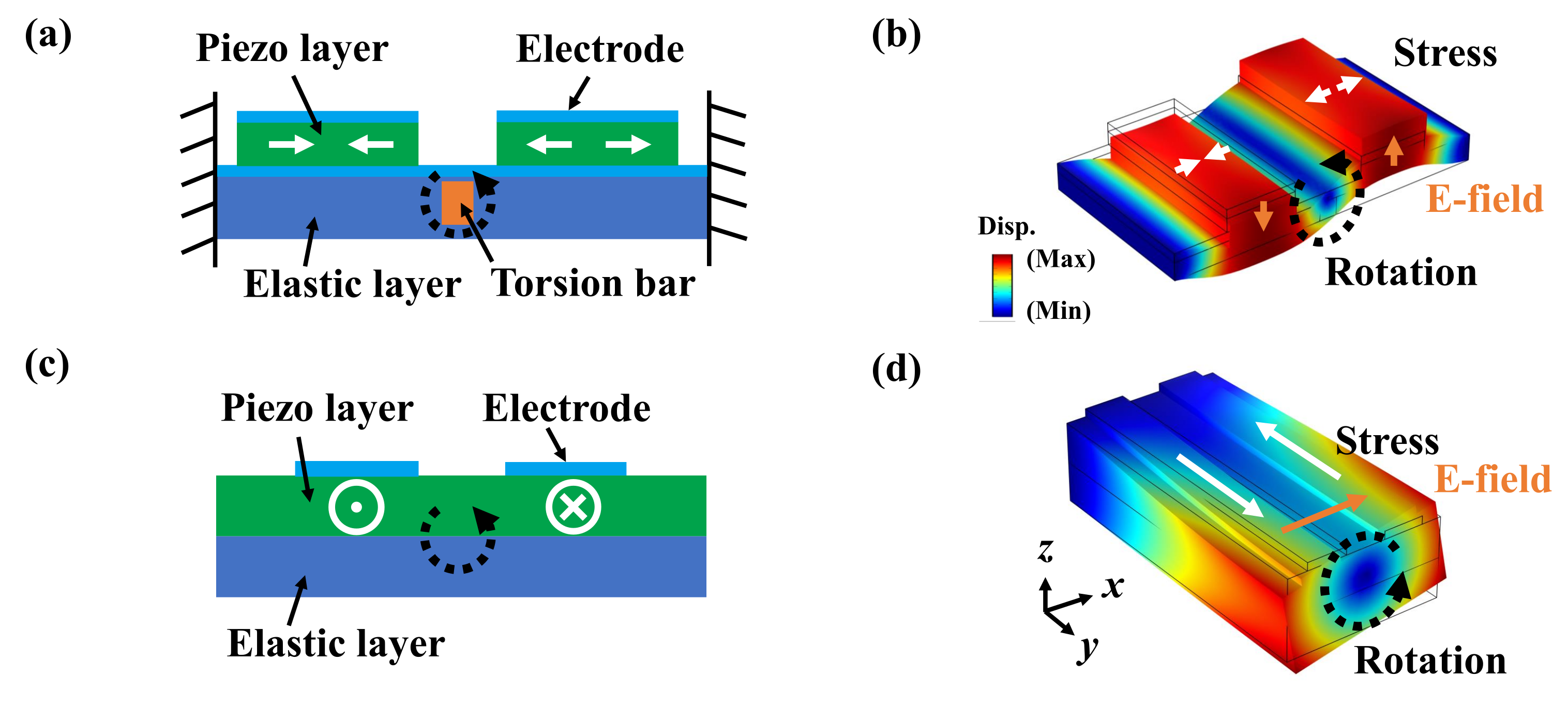
2.1. Principle of e 16 Torsional Actuator

The e 16 driven principle is rarely mentioned, possibly due to the lack of strong e 16 piezoelectric thin-film. The commonly used piezoelectric thin-film, such as PZT, AlN, ZnO and AlScN, e 16 is zero, while LN has a strong e 16 up to −4.5 C / m 2 . On the contrary, the driven principle of e 31 actuators have been well studied. In order to facilitate understanding and comparison of the difference between two driven methods, the e 31 driven principle is briefly introduced first.
The section view of e 31 torsional actuator is shown in Figure 1a, which consists of two cantilevers and a torsion bar. Two cantilevers are fixed at one end, and the torsion bar is perpendicularly connected to the middle. Via the piezoelectric coefficient e 31 translates the E-field in z direction to the strain/stress in x direction, the voltage in opposite polarity generate opposite stress. Due to the difference in stress between the piezo and elastic layers, the cantilevers are bent up or down [39]. The bending motion of two cantilevers twist the middle point and then rotates the torsion bar, which is shown in Figure 1b. The e 31 actuators drive the torsion bar indirectly, and the stress/strain of them can only act on the root of the torsion bar.
Contrary to the e 31 torsional actuators, the e 16 actuators generate stress over the entire torsion bar and convert the voltage into the driven force directly, consequently achieving high deflection. The section view of the e 16 torsional actuator is shown in Figure 1c. There are two electrodes covered on the torsion bar. When the voltage is applied to each pair of electrodes, the E-field generates in x direction. With the e 16 piezoelectric transduction, a pair of opposing stresses are generated in the x y plane along the electrodes. One electrode produces tensile stress and deflects downwards, and the other electrode generates compressive stress and deflects upward. So, the torsion bar rotates around the y-axis, which is shown in Figure 1d.
With e 16 actuation principle, the 2D scanners can be easily implemented by driving two orthogonal e 16 -actuated torsional bars within the x y plane, which require large e 16 on two orthogonal propagation angles. Due to the strong anisotropy of the LN crystal to effectively drive the dual-axis scanner, the orientation of LN needs to be carefully considered.

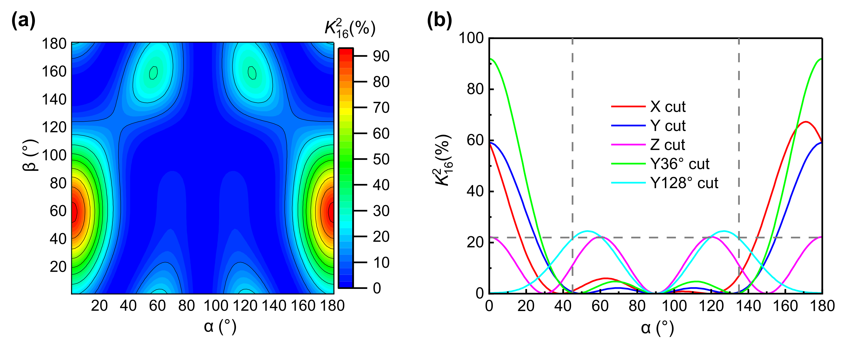
2.2. Euler Angle for LN
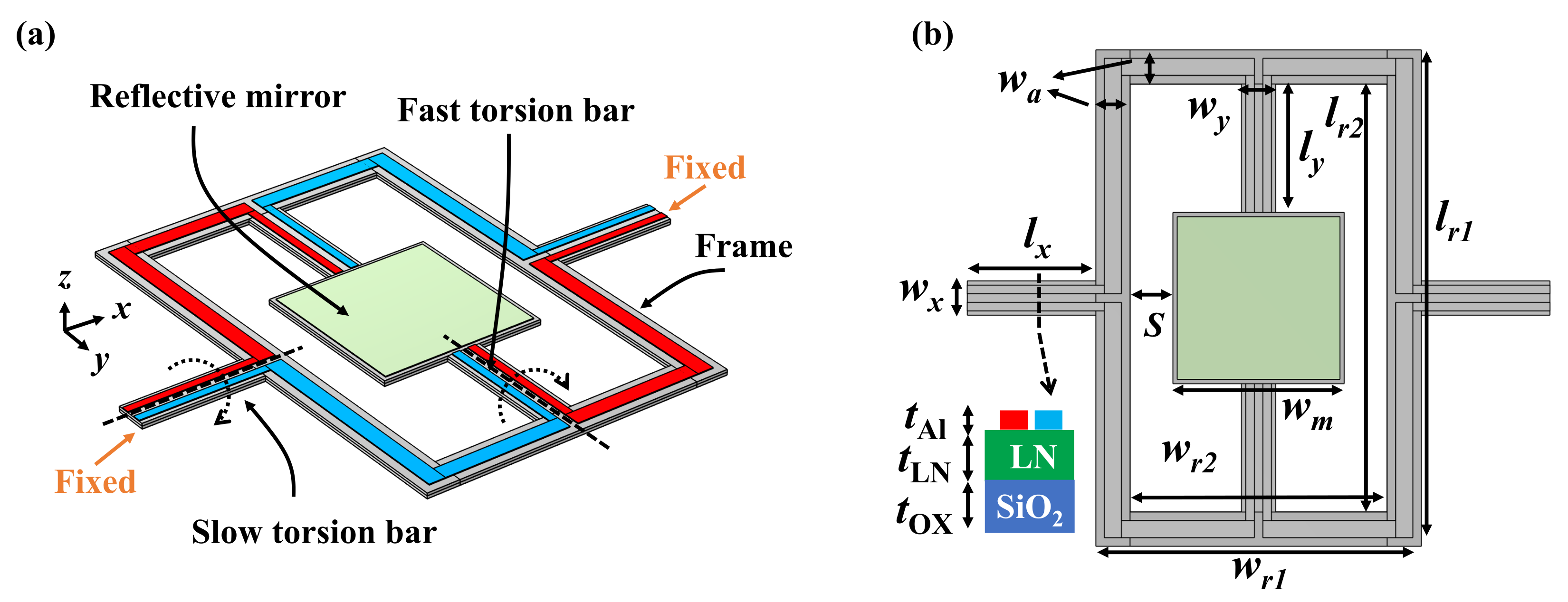
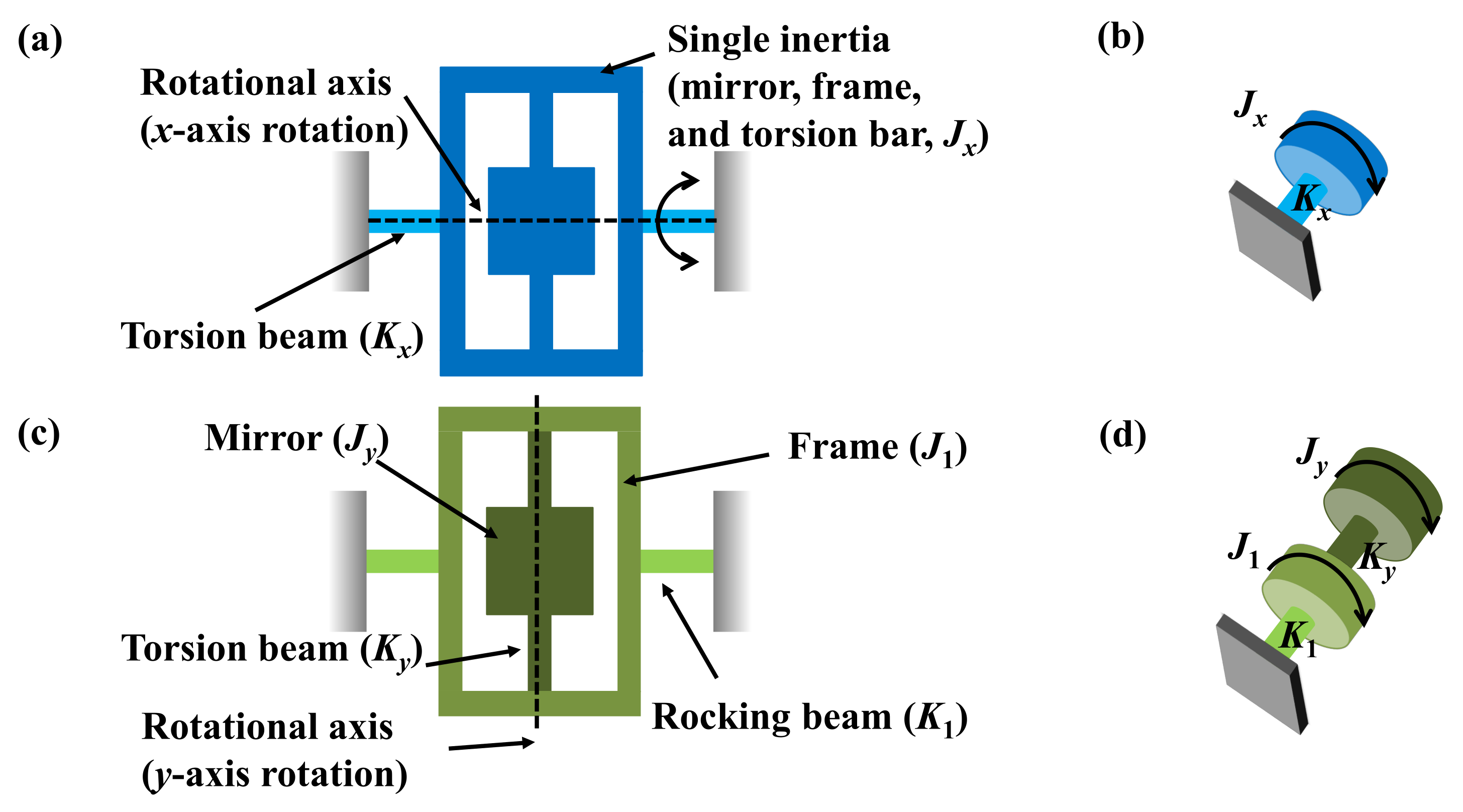
The e 16 of LN crystal varies enormously with different Euler angles, while the output efficiency of the bending actuator is proportional to the material electro-mechanical coupling factor ( K 2 ) that is positively related to the piezoelectric constant [40]. The K 2 measures the conversion efficiency between electrical and mechanical energy of a material and is defined as [41]:
K i j 2 = e i j 2 ε i i T c j j E
where i is the electrical field direction (1 for x and 3 for z) and j is the stress direction; e i j is the piezoelectric stress constant in the direction of the electric field and mechanical stress, ε i i T is permittivity in the direction of the electric field at zero stress and c j j E is elastic stiffness at zero electric field.
The variation of K 16 2 with Euler angle is explored to find the optimal orientation for dual-axis scanner. The material properties (piezoelectric constant, dielectric permittivity and elastic stiffness) of LN with different orientations are calculated based on the Euler angle transformation, which follows the order of Z-X-Z [42]. The Euler angle is expressed by ( α , β and γ ), where α is the propagation angle which determines the placement direction of electrodes on the cut plane.
High K 16 2 on two orthogonal in-plane directions is required to drive the dual-axis scanner. The K 16 2 contour plot of LN with Euler angle of ( α , β , 0 ) is shown in Figure 2a. The cut plane has the Euler angle of ( α , β , 0 ) and is named as rotated Y-cut [43]. The orientations with γ 0 except X cut are not referred to in this paper because they are seldom used, and do not have bimodal properties such as rotated Y cut. There are two maximum values of K 16 at the cut plane with β = 150 , which is Y120 -cut. However, Y120 -cut LN is rarely mentioned and has never been demonstrated in devices.
Among the commonly used orientations, Y128 cut is closest to Y120 cut and has K 16 2 of 22% at both α = 45 and 135 . The K 16 2 of commonly used orientations is shown in Figure 2b. There is one maximum of K 16 2 up to 92% at Y36 cut, thus it has demonstrated a high driven efficient in 1D MEMS scanners [38]. However, its K 16 2 at the orthogonal direction of the maximum value ( α = 90 ) is 0, which makes Y36 cut unappropriated for the K 16 2 -actuated dual-axis scanner. Thus, the Y128 -cut LN thin-film is chosen for the following analysis.

2.3. Structure

The proposed dual-axis MEMS scanner can perform 2D scanning with a single voltage port, which simplifies the connection with control circuits. The schematic view and electrode configuration of the proposed scanner structure are shown in Figure 3a. The proposed MEMS scanner is comprised of a reflective micro-mirror, a frame and two pairs of torsional bars with driving electrodes on top. The torsional bars are divided into fast and slow torsional bars according to the frequency of the correspondence scanning mode. The fast torsion bars rotate along the y-axis, while slow torsion bars rotate along the x-axis. The reflective mirror is connected to the frame with a pair of fast torsion bars, while the frame is connected to the substrate with a pair of slow torsion bars. The actuation principle of torsion bars has been elaborated in Section 2. A pair of voltage with opposite polarity are applied to two ends of the torsion bars, as illustrated in Figure 3a, in which electrodes in blue/red are connected to ground/positive, respectively. After the ground/positive voltages are, respectively, connected in external routing, the proposed scanner can perform 2D scanning with single port rather than multiple port connections in some e 31 -actuated schemes [44,45,46], reducing the complexity of the control circuits.
The top view of the proposed 2D MEMS resonant scanner labeled with the main geometry dimensions is shown in Figure 3b, and the inset shows the cross-section of the torsion bar. The resonant scanner consists of LN, SiO 2 and Al layers. The SiO 2 layer serves as the elastic layer, while Al layer serves as the driving electrodes and reflective layer. The torsion bars are placed along in-plane angle α of 45 and 135 to align with two maximum K 16 2 in the Y128 cut.
The critical geometry dimensions and corresponding descriptions are listed in Table 1 and set as default value, including the width/length of torsion bars, mirror size, thickness of LN/SiO 2 /Al layers and the size of the frame. The thickness of the LN thin film through the transfer technique is mainly in the range of 0.2–1 μ m [32,33,34,35,36]. Considering the trade-off between mechanical strength (dynamic deformation [12]) and resonant frequency, 0.55 μ m-thick LN film is selected for the following analysis.

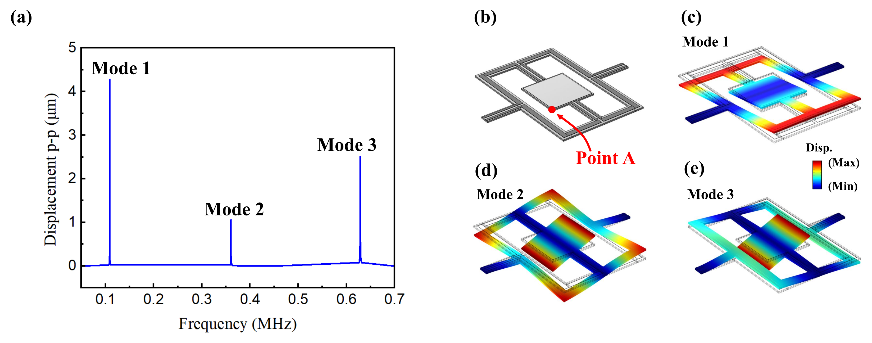
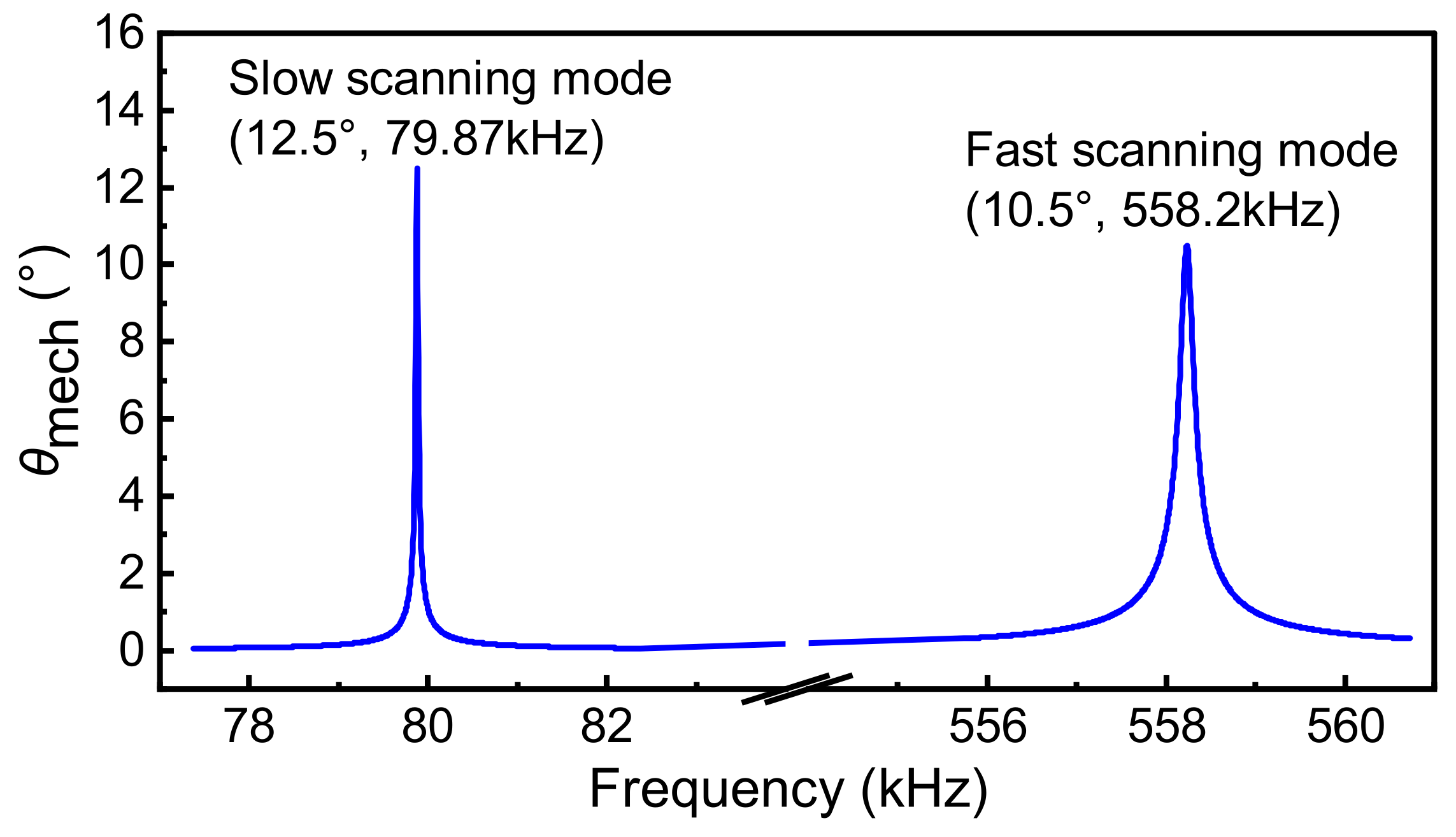
2.4. Frequency Response and Mode Shapes

The simulated peak-to-peak (p-p) displacement frequency response of point A on the proposed scanner with 1 V driving voltage is shown in Figure 4a. The location of point A is shown in Figure 4b. Figure 4a is obtained by the frequency domain analysis of COMSOL, while the mode shapes in Figure 4c–e are obtained by the eigenfrequency analysis. Large displacement within the spectrum exists in three modes, which are labeled as Mode 1–3, and corresponding mode shapes are shown in Figure 4c–e. Modes 1–3 represent the torsion modes of the outer frame, the rocking mode of the outer frame in-phase with mirror and the rocking mode of the outer frame out-phase with mirror. Mode 1 is selected as the slow scanning mode, in which the reflective mirror and the frame rotate as a whole body around the x-axis at 109 kHz. Mode 3 is selected as the fast scanning mode, which exhibits higher frequency and deflection than Mode 2. In Mode 3, the mirror rotates around the y-axis at 629 kHz, and the outer frame performs a rocking motion out of phase with the mirror.

3. Analytical Modeling

In order to obtain a physical insight into how geometric parameters affect scanner performance, an analytical model is developed. This model is inspired by [12,47]. The physical behavior of the MEMS scanner can be predicted with a set of second-order differential equations of motion which are obtained in terms of angular deflection and moment of inertia, damping coefficient and effective spring constant as parameters. By solving the equations in the frequency domain, the most concerning performance, including the resonant frequencies, maximum angular deflection and FoM can be roughly estimated.

3.1. Resonant Frequency

The schematic diagram and the lumped-parameter model for the rotation spring-mass-damping system of fast and slow scanning modes for the proposed scanner are shown in Figure 5. Figure 5a,c show the schematic diagram of fast and slow scanning modes and labels with the physical quantities associated with the structure. The rotation spring-mass-damping model for fast and slow scanning modes are shown in Figure 5b,d, respectively.
For slow scanning mode, the moment of inertia of the mirror, frame and fast torsion bars are combined as a single body ( J x ) and rotate along the x-axis by torsion beam with torsional stiffness K x . Therefore, the slow scanning mode can be expressed by a single equation of motion.
J x θ ¨ x + c x θ x + K x θ x = T x
where θ x is the mechanical rotation angle of the slow scanning mode, J x is the effective moment of inertia of the total resonate body, K x is the torsional stiffness of the slow torsion beam, c x is the mechanical damping of the slow scanning mode and T x is the torque generated by electrodes placed along the x-axis.
For fast scanning mode, the mirror is located at the end of the system and is connected to the frame with fast torsion beams, while the frame is connected to the supporting substrate with rocking beams. The moment of inertia of the mirror and frame along the y-axis are expressed by J y and J 1 , which are series-connected by spring elements ( K y and K 1 ). The torque is generated on fast torsion beams then acts on the mirror. Assume that the structure components except the torsion and rocking beams are rigid bodies, the equations of motion for slow and fast scanning can be expressed by:
J y θ ¨ y + c y ( θ ˙ y θ ˙ 1 ) + K y ( θ y θ 1 ) = T y J 1 θ ¨ 1 + ( c 1 + c y ) θ ˙ 1 c y θ ˙ y + ( K 1 + K y ) θ 1 K y θ y = 0
where θ y , θ 1 are the mechanical rotation angles of mirror and frame in fast scanning, respectively; J y , J 1 are the effective moment of inertia of the mirror and frame, respectively; K y , K 1 are the torsional stiffness of the fast torsion bar and spring constant of the slow torsion bar in rocking mode, respectively; c y and c 1 are the effective damping of mirror and frame, respectively; T y is the torque generated by the electrode placed along the y-axis.
Given the torsional stiffness and effective moment of inertia, the resonant frequency can be obtained. Ignoring the damping of the mechanical system, with angular momentum balance ( T x = 0 or T y = 0 ), the resonant frequency of slow/fast scanning mode is
f x = K x / J x / 2 π
f y = K y / J y / 2 π
The torsional stiffness ( K x , K y ) and spring constant ( K 1 ) are
K x = 2 G x I x / l x
K y = 2 G y I y / l y
K 1 = E w x t 3 ( 2 + 6 ( 1 + w r 1 / l x ) 2 ) / ( 12 l x )
where G x , G y and E are the effective stiffness of c 44 , c 55 and c 11 weighted by material thickness percentage, respectively; I x and I y are the polar moment of inertia for the slow and fast torsion bars expressed by [12]
I x = w x t 3 ( 16 / 3 3.36 t w x ( 1 t 4 12 w x 4 ) ) I y = w y t 3 ( 16 / 3 3.36 t w y ( 1 t 4 12 w y 4 ) )
The effective moment of inertia of the same object may have different calculated expressions. J x includes the contributions of the resonant body and torsional beam in slow scanning. J y includes the contributions of the mirror and torsional beam in fast scanning. J 1 includes the contributions of the frame and rocking beam in fast scanning. Thus, the effective moments of inertia are expressed by [47]
J x = J m , x x + J f r , x x + J f t , x x + ( 1 / 3 ) J s t , x x J y = J m , y y + ( 2 / 3 ) J f t , y y J 1 = J f r , y y + 2 J s t , y y
where J m , x x , J f t , x x , J f r , x x , J s t , x x is the moment of inertia of the mirror, fast torsion bar, frame and slow torsion bar when they rotate around the x-axis in slow scanning; J m , y y , J f t , y y , J f r , y y and J s t , y y are the moments of inertia of the mirror, frame, fast torsion bar and slow torsion bar when they rotate around the y-axis in fast scanning:
J m , x x = ρ e t w m l m 3 / 12 J f t , x x = ρ e t w y ( l r 2 3 l m 3 ) / 12 J f r , x x = ρ e t ( w r 1 l r 1 3 w r 2 l r 2 3 ) / 12 J s t , x x = ρ e t l x w x 3 / 12
J m , y y = ρ e t l m w m 3 / 12 J f t , y y = ρ e t l y w y 3 / 12 J f r , y y = ρ e t ( l r 1 w r 1 3 l r 2 w r 2 3 ) / 12 J s t , y y ρ e t l x w x t ( 0.01 l x 2 + 0.05 l x w r 1 + 0.1 w r 1 2 )
where ρ e is the effective density of stack layers.

3.2. Angular Deflection

Given the geometric parameters and torque, deflection can be obtained. The angular deflection of the mirror can be obtained by Laplace transform, with a static solution of the momentum balance; the mechanical deflections are expressed by
θ x = T x / K x
θ y = T y ( 1 / K 1 + 1 / K y )
By analogy to the torque of e 31 actuator [48], the piezoelectric torque of e 16 actuator can be estimated by:
T k = 1 2 E ¯ k w k d 16 , k E i k [ 2 z ¯ t i 2 t i Σ j = 1 i t j + t i 2 ]
where the subscript k can be replaced by x and y to represent x or y direction; subscript i represents the i layer, i = 1,2 and SiO 2 /LN, respectively; w k is the width of torsion bar; d 16 , k is piezoelectric stress constant; E ¯ i is the electric field component ( E ¯ k = V / p k , where p k is the pitch of two electrodes, which is w k / 2 in this work); E i k is the elastic modulus of the i layer in k direction and t i is the thickness of the i layer. The position of neutral axis z ¯ is given by:
z ¯ = i = 1 N E i k t i 2 2 i = 1 N E i k t i j = 1 i t j 2 i = 1 N E i k t i
Equation (4) shows that the torque is determined by layer thickness and material constant (elastic modulus and piezoelectric constant), when the applied voltage V is given. The high piezoelectricity results in high driving torque/force, thus achieving high deflection as presented in [40]. Additionally, the high electro-mechanical coupling K 2 helps high driven efficiency. The Y128 -cut LN offers a piezoelectric constant d 16 of 45 pC / N , which is comparable with the d 31 of PZT (~100 pC / N [31,49]) and is about 20 times AlN (2 pC / N [50]). A rough calculation shows that the order of the torque is 10 7 N·m at 1 V in Y128 -cut LN.

3.3. Figure of Merit

The pixel scanning rate of the 2D scanner is determined by the θ opt · D · f product of the fast mode [6,11], thus it is employed as the figure of merit (FoM) in this work. With θ opt = θ y , D = w m , f = f y and previous derivation of frequency and deflection, the FoM are
F o M = θ opt · D · f = 4 T y ( 1 / K 1 + 1 / K y ) · w m · K y / J y / ( 2 π ) = 4 T y ( 1 + K y / K 1 ) · w m / ( 2 π K y J y )
K 1 is typically higher than K y , and θ y is dominated by K y . Assuming K 1 K y , given the material properties and voltage, a relationship depending only on the geometric parameter can be obtained:
F o M l y w y L m W m G K
where G K = ( 5.33 3.36 t / w y ) ( 1 t 4 / ( 12 w y 4 ) [12]. Equation (5) shows the correlation between FoM and geometric parameters, the FoM of the scanner is positively correlated with l y and negatively correlated with w y , L m , W m and t. It is worth mentioning that the purpose of Equation (5) is only to give a physical intuition, it is established when K 1 K y , otherwise the actual FoM is still affected by K 1 .

4. Simulation Results

4.1. Simulation Setup

To better understand the dynamic characteristics of the proposed device and validate the analytical model, 3D FEM analysis and optimization have been performed using COMSOL software. The 3D schematic view of the FEM model is shown in Figure 3a with default geometry parameters listed in Table 1. Unless specified, only one parameter is changed in each parameter sweep, and the other parameters in the list remain default values.
The specific settings of the simulation are as follows. The piezoelectric device module is adopted in simulation. The Euler angle of LN is set to ( 45 , 38 , 0 ) and aligns with the x-axis torsion bars to utilize the unique bimodal characteristic. In solid mechanics module, the fixed boundaries are applied to two ends of the slow torsion bar, and the damping of materials are all set to 1/1000. In static electricity module, the electrodes in red and blue are connected to the terminal of 1 V and ground, respectively. The simulation with these settings shows the behavior of device with material loss in vacuum (without air damping). The default parameters in COMSOL are used in the simulation.
As with the simulation, the calculation of the analytical model uses default parameters in COMSOL. The density, elastic modulus and shear modulus of SiO 2 are 2200 kg / m 3 , 70 GPa, and 29.9 GPa, respectively. The densities, c 11 , c 44 and c 55 of 128 Y-cut LN with Euler angle of ( 45 , 38 , 0 ) are 4700 kg / m 3 , 213.5 GPa, 66.1 GPa and 66.1 GPa, respectively.

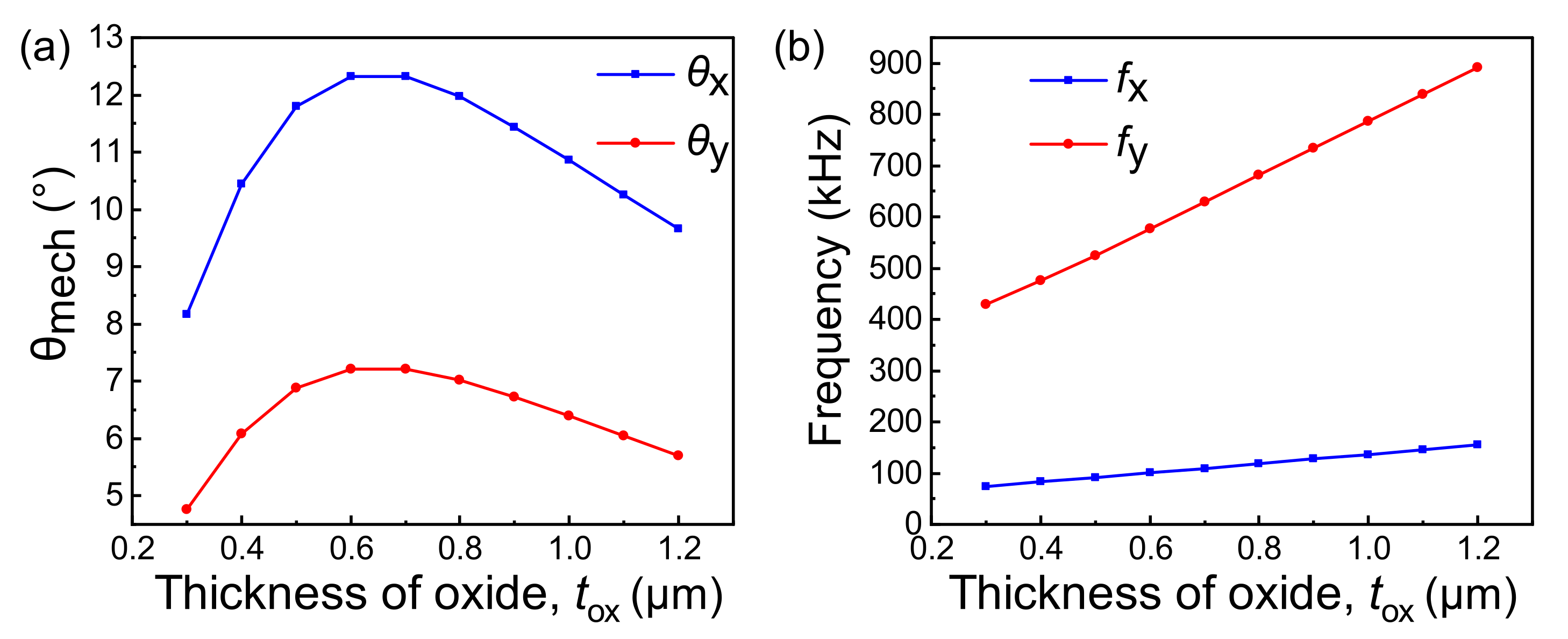
4.2. Layer Thickness

The torsional stiffness K, moment of inertia J and the piezoelectric torque T are significantly affected by total thickness, thus affecting the frequency and angular deflection of the MEMS scanner. Intuitively, the smaller t leads to smaller torsional stiffness, which leads to larger deflection angle and lower frequency, especially higher FoM (Equation (5)). However, the reduction in mechanical strength results in larger dynamic deformation [12]. Considering the compromise with dynamic deformation and FoM, t LN is set to 0.55 μ m, since the 128 Y-cut LN thin film in such thickness is available and has been applied in the resonators [51].
There is an optimal t Ox for maximum deflection at given t LN . Figure 6a,b show that the mechanical deflection and frequency of both fast and slow sacnning modes vary with different thicknesses of SiO 2 . According to Equation (Section 3.1), the frequencies of both modes should increase linearly with t Ox , since total thickness increases. Interestingly, when the t Ox is 0.7 μ m, which is about 1.25 times of t LN , the mechanical deflection of both modes reach the maximum value simultaneously. Thus, t Ox is set to 0.7 μ m by default. The optimal ratio of t o x / t L N can not be predicted by the exiting model in this work. However, the research of the torque produced by the e 16 actuation is still blank, an analytical model of e 16 piezoelectric actuation may require further study.

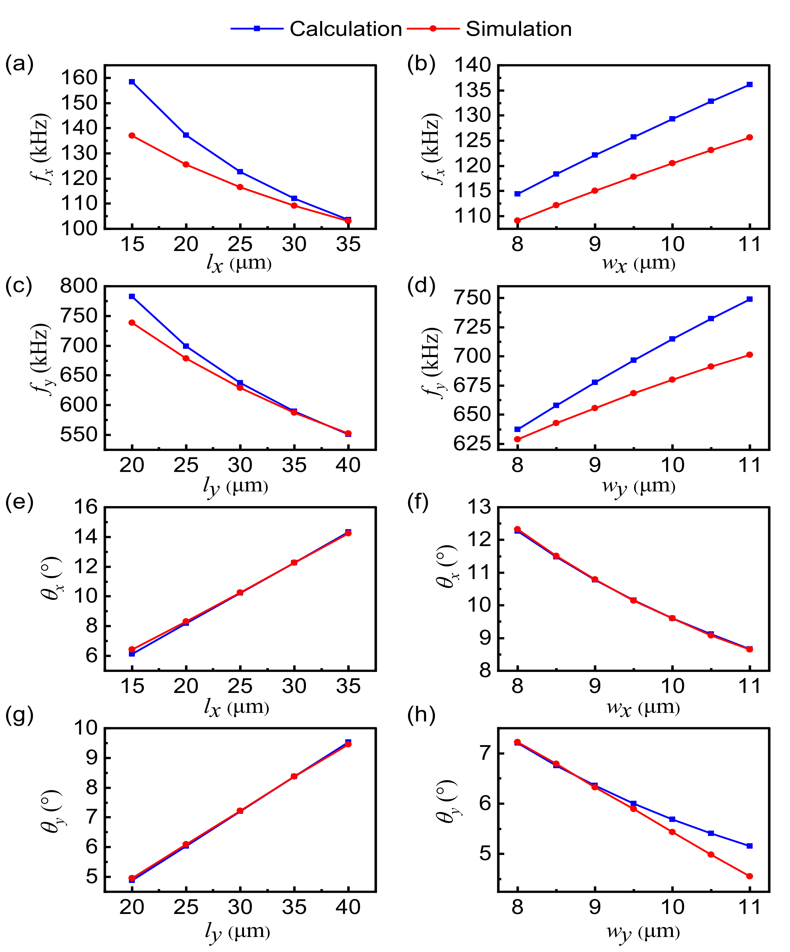
4.3. Geometry Parameters

According to Equation (Section 3.1), given the thicknesses of layers and material properties, there are four geometry parameters ( l x , w x , l y and w y ) that determine the stiffness of corresponding modes. l x and w x determine the torsional stiffness of the slow scanning mode, while l y and w y determine the torsional stiffness of the fast scanning mode. Figure 7a–d show the effect on the resonant frequency of variations with l x , w x , l y and w y , while Figure 7e–h show the effect on the mechanical deflection angle of variations with l x , w x , l y and w y , respectively.
As an example, the impact of l x and w x on slow scanning mode is elaborated here, while the effect of l y and w y on fast scanning mode is similar to it and is briefly described later. In slow scanning mode, most of the mass is concentrated in the mirror and frame, as a rough calculation, the total moment of inertia is assumed to be constant. As Equations (1a), (2a) and (3a) describe, the torsional stiffness K x is inversely proportional to l x , thus the resonant frequency of slow scanning mode ( f x ) is inversely proportional to the square root of l x , while mechanical angular deflection in slow scanning mode ( θ x ) is proportional to l x . The calculation and simulation curves of f x and θ x varying with l x are shown in Figure 7a,e, respectively. The simulated result of f x coincides with the calculated result with a maximum error of 13%. The error comes from neglecting the moment of inertia of the Al electrodes. As in Equation (4), when t and V are given, T is a constant independent of l x and set to 1.003 × 10 7 N·m, thus θ x l x . This inference is completely consistent with Figure 7e.
Similarly, the effect of w x to f x and θ x can be disclosed by combining with Equations (1a), (2a) and (3a). With constant T and J x , f x is positively correlated with w x , while θ x is negatively correlated with w x . The curves of f x and θ x varying with w x are shown in Figure 7b,f. The calculated result of θ x is consistent with the simulated curve, which indicates that the torsional stiffness calculation is quite accurate, while f x is affected by the inaccurate J x , which neglects the moment of inertia of the Al electrodes.
The effect of l y and w y to fast scanning mode is similar with l x and w x to slow scanning mode. It is worth mentioning that there is a significant deviation in Figure 7h between the simulated and calculated curve due to the inaccurate rocking stiffness K 1 , since the frame is not a perfectly rigid body. Moreover, to enlarge θ y , the angular resonant frequency of the frame should be matched to the mirror plate. i.e., K 1 / J 1 should be matched to K y / J y , otherwise the mirror plate would be out of sync with the frame and cause resonance to disappear.
After optimization, l y and w a are set to 35 μ m and 12 μ m respectively, while other parameters are kept in default. Figure 8 shows the frequency response of the mechanical deflection angle for the fast and slow scanning modes, respectively. The mechanical deflection θ x and θ y reach 12.5 and 10.5 , corresponding to the optical deflection angle of 50 and 42 , at 79.9 kHz and 558.2 kHz, respectively. Table 2 lists the MEMS scanner performance of this work and the state of arts of the 2D MEMS scanner, which shows that this work has advantages in driving voltage, deflection, frequency and FoM and great advantages in deflection per volt. The FoM of fast scanning mode in this work reaches 938 · mm · kHz .

5. Conclusions

We have proposed a 128°Y-cut LN thin-film-based dual-axis torsional MEMS resonant scanner for the first time and provided an analytical model. The calculation results are in good agreement with the FEA simulations, confirming the validity of the analytical model. After optimization, the proposed resonant scanner achieves an θ opt · D · f up to 937.8 · mm · kHz in FEA simulation, which is superior to most e 31 piezoelectric-actuated 2D MEMS scanner. The simulated optical deflection angle in the x-axis and y-axis are 50 and 42 at 1 V, corresponding to frequencies of 79.9 kHz and 558.2 kHz, respectively.
The main finding are as follows:
  • The Lithium niobate on insulation (LNOI) can be a novel and promising platform to design MEMS scanner/actuator. The transferred LN crystal provides high piezoelectricity that is much higher than AlN, with ZnO comparable to PZT, and a high quality factor, smooth surface and high strength.
  • A novel principle of the torsional actuator, the electric field is directly applied to the torsion bar. With e 16 transduction, the torsion bar is driven directly, resulting in high deflection.
  • The unique bimodal of e 16 of Y128 -cut LN can be utilized in the 2D scanner. The proposed scanner performs 2D scanning with a single port reducing the complexity of the control circuit.
With the superior performance of high frequency, high deflection per volt and high figure of merit ( θ opt · D · f ) in low driving voltage, the proposed MEMS scanner is a promising candidate for fast scanner applications (e.g., wavelength-selective switches and submicron biomedical systems), especially the application of LiDAR in mobile devices or micro-robotics. We hope that more efficient actuators utilizing the e 16 -actuated principle on the LNOI platform will be developed. The following work includes the fabrication and experimental measurement of the proposed resonant scanner, and the refinement of the e 16 piezoelectric actuation analytical model.

Author Contributions

Y.L.: design, simulation, graphics and original draft preparation; K.L.: validation, formal analysis, theoretical model, review and editing; T.W.: supervision, project administration and editing. All authors have read and agreed to the published version of the manuscript.

Funding

This work was supported by the National Natural Science Foundation of China (61874073), Natural Science Foundation of Shanghai (19ZR1477000) and ShanghaiTech Start-up Fund.

Institutional Review Board Statement

Not applicable.

Informed Consent Statement

Not applicable.

Data Availability Statement

Data sharing not applicable.

Conflicts of Interest

The authors declare no conflict of interest.

References

  1. An, Y.; Sun, B.; Wang, P.; Xiao, L.; Liu, H.; Xie, H. A 1 × 20 MEMS mirror array with large scan angle and low driving voltage for optical wavelength-selective switches. Sens. Actuators A Phys. 2021, 324, 112689. [Google Scholar] [CrossRef]
  2. Petrak, O.; Schwarz, F.; Pohl, L.; Reher, M.; Janicke, C.; Przytarski, J.; Senger, F.; Albers, J.; Giese, T.; Ratzmann, L.; et al. Laser beam scanning based AR-display applying resonant 2D MEMS mirrors. In Optical Architectures for Displays and Sensing in Augmented, Virtual, and Mixed Reality (AR, VR, MR) II; International Society for Optics and Photonics: Bellingham, WA, USA, 2021; Volume 11765, p. 1176503. [Google Scholar]
  3. Druml, N.; Maksymova, I.; Thurner, T.; van Lierop, D.; Hennecke, M.; Foroutan, A. 1D MEMS micro-scanning LiDAR. In Proceedings of the Conference on Sensor Device Technologies and Applications, Venice, ltaly, 16 September 2018; Volume 9. [Google Scholar]
  4. Kasturi, A.; Milanovic, V.; Atwood, B.H.; Yang, J. UAV-borne lidar with MEMS mirror-based scanning capability. In Laser Radar Technology and Applications XXI; SPIE: Bellingham, WA, USA, 2016; Volume 9832, pp. 206–215. [Google Scholar] [CrossRef]
  5. Pengwang, E.; Rabenorosoa, K.; Rakotondrabe, M.; Andreff, N. Scanning micromirror platform based on MEMS technology for medical application. Micromachines 2016, 7, 24. [Google Scholar] [CrossRef] [PubMed]
  6. Holmström, S.T.; Baran, U.; Urey, H. MEMS laser scanners: A review. J. Microelectromech. Syst. 2014, 23, 259–275. [Google Scholar] [CrossRef]
  7. Wang, D.; Watkins, C.; Xie, H. MEMS Mirrors for LiDAR: A review. Micromachines 2020, 11, 456. [Google Scholar] [CrossRef]
  8. Wang, D.; Xie, H.; Thomas, L.; Koppal, S.J. A Miniature LiDAR with a Detached MEMS Scanner for Micro-Robotics. IEEE Sens. J. 2021, 21, 21941–21946. [Google Scholar] [CrossRef]
  9. Luetzenburg, G.; Kroon, A.; Bjørk, A.A. Evaluation of the Apple iPhone 12 Pro LiDAR for an Application in Geosciences. Sci. Rep. 2021, 11, 22221. [Google Scholar] [CrossRef]
  10. Gupta, S.; Lohani, B. Augmented reality system using lidar point cloud data for displaying dimensional information of objects on mobile phones. In ISPRS Annals of the Photogrammetry, Remote Sensing and Spatial Information Sciences; Copernicus GmbH: Göttingen, Germany, 2014; Volume II-5, pp. 153–159. [Google Scholar] [CrossRef] [Green Version]
  11. Baran, U.; Brown, D.; Holmstrom, S.; Balma, D.; Davis, W.O.; Muralt, P.; Urey, H. Resonant PZT MEMS Scanner for High-Resolution Displays. J. Microelectromech. Syst. 2012, 21, 1303–1310. [Google Scholar] [CrossRef] [Green Version]
  12. Urey, H. Torsional MEMS scanner design for high-resolution scanning display systems. In Optical Scanning 2002; International Society for Optics and Photonics: Bellingham, WA, USA, 2002; Volume 4773, pp. 27–37. [Google Scholar]
  13. Wang, Q.; Wang, W.; Zhuang, X.; Zhou, C.; Fan, B. Development of an Electrostatic Comb-Driven MEMS Scanning Mirror for Two-Dimensional Raster Scanning. Micromachines 2021, 12, 378. [Google Scholar] [CrossRef]
  14. Li, H.; Duan, X.; Li, G.; Oldham, K.R.; Wang, T.D. An Electrostatic MEMS Translational Scanner with Large Out-of-Plane Stroke for Remote Axial-Scanning in Multi-Photon Microscopy. Micromachines 2017, 8, 159. [Google Scholar] [CrossRef] [Green Version]
  15. Hung, A.C.L.; Lai, H.Y.H.; Lin, T.W.; Fu, S.G.; Lu, M.S.C. An electrostatically driven 2D micro-scanning mirror with capacitive sensing for projection display. Sens. Actuators A Phys. 2015, 222, 122–129. [Google Scholar] [CrossRef]
  16. Sun, C.; Liu, Y.; Li, B.; Su, W.; Luo, M.; Du, G.; Wu, Y. Modeling and Optimization of a Novel ScAlN-Based MEMS Scanning Mirror with Large Static and Dynamic Two-Axis Tilting Angles. Sensors 2021, 21, 5513. [Google Scholar] [CrossRef] [PubMed]
  17. Hung, E.; Senturia, S. Extending the travel range of analog-tuned electrostatic actuators. J. Microelectromech. Syst. 1999, 8, 497–505. [Google Scholar] [CrossRef]
  18. Yu, H.; Zhou, P.; Shen, W. Fast-scan MOEMS Mirror for HD Laser Projection Applications. In Proceedings of the 2021 IEEE 16th International Conference on Nano/Micro Engineered and Molecular Systems (NEMS), Xiamen, China, 25–29 April 2021; pp. 265–269. [Google Scholar]
  19. Kim, S.; Lee, C.; Kim, J.Y.; Kim, J.; Lim, G.; Kim, C. Two-axis polydimethylsiloxane-based electromagnetic microelectromechanical system scanning mirror for optical coherence tomography. J. Biomed. Opt. 2016, 21, 106001. [Google Scholar] [CrossRef] [PubMed]
  20. Ju, S.; Jeong, H.; Park, J.H.; Bu, J.U.; Ji, C.H. Electromagnetic 2D scanning micromirror for high definition laser projection displays. IEEE Photonics Technol. Lett. 2018, 30, 2072–2075. [Google Scholar] [CrossRef]
  21. Zhou, Y.; Wen, Q.; Wen, Z.; Huang, J.; Chang, F. An electromagnetic scanning mirror integrated with blazed grating and angle sensor for a near infrared micro spectrometer. J. Micromech. Microeng. 2017, 27, 125009. [Google Scholar] [CrossRef] [Green Version]
  22. Seo, Y.H.; Hwang, K.; Park, H.C.; Jeong, K.H. Electrothermal MEMS fiber scanner for optical endomicroscopy. Opt. Express 2016, 24, 3903–3909. [Google Scholar] [CrossRef] [PubMed]
  23. Zhou, L.; Yu, X.; Feng, P.X.L.; Li, J.; Xie, H. A MEMS lens scanner based on serpentine electrothermal bimorph actuators for large axial tuning. Opt. Express 2020, 28, 23439–23453. [Google Scholar] [CrossRef]
  24. Tanguy, Q.A.; Gaiffe, O.; Passilly, N.; Cote, J.M.; Cabodevila, G.; Bargiel, S.; Lutz, P.; Xie, H.; Gorecki, C. Real-time Lissajous imaging with a low-voltage 2-axis MEMS scanner based on electrothermal actuation. Opt. Express 2020, 28, 8512–8527. [Google Scholar] [CrossRef]
  25. Karpelson, M.; Wei, G.Y.; Wood, R.J. A review of actuation and power electronics options for flapping-wing robotic insects. In Proceedings of the 2008 IEEE International Conference on Robotics and Automation, Pasadena, CA, USA, 19–23 May 2008; pp. 779–786. [Google Scholar] [CrossRef]
  26. Uchino, K. Piezoelectric actuators 2006. J. Electroceramics 2008, 20, 301–311. [Google Scholar] [CrossRef]
  27. Eom, C.B.; Trolier-McKinstry, S. Thin-film piezoelectric MEMS. MRS Bull. 2012, 37, 1007–1017. [Google Scholar] [CrossRef] [Green Version]
  28. Shkir, M.; Arif, M.; Ganesh, V.; Manthrammel, M.; Singh, A.; Yahia, I.; Maidur, S.R.; Patil, P.S.; AlFaify, S. Investigation on structural, linear, nonlinear and optical limiting properties of sol-gel derived nanocrystalline Mg doped ZnO thin films for optoelectronic applications. J. Mol. Struct. 2018, 1173, 375–384. [Google Scholar] [CrossRef]
  29. Shao, J.; Li, Q.; Feng, C.; Li, W.; Yu, H. AlN based piezoelectric micromirror. Opt. Lett. 2018, 43, 987–990. [Google Scholar] [CrossRef]
  30. Tang, J.; Niu, D.; Tai, Z.; Hu, X. Deposition of highly c-axis-oriented ScAlN thin films at different sputtering power. J. Mater. Sci. Mater. Electron. 2017, 28, 5512–5517. [Google Scholar] [CrossRef]
  31. Yuan, J.R.; Jiang, X.; Snook, K.; Rehrig, P.W.; Shrout, T.R.; Hackenberger, W.S.; Cheng, A.; Cao, P.; Lavalelle, G.; Geng, X. 5I-1 Microfabrication of Piezoelectric Composite Ultrasound Transducers (PC-MUT). In Proceedings of the 2006 IEEE Ultrasonics Symposium, Vancouver, BC, Canada, 2–6 October 2006; pp. 922–925. [Google Scholar] [CrossRef]
  32. Wang, C.; Zhang, M.; Chen, X.; Bertrand, M.; Shams-Ansari, A.; Chandrasekhar, S.; Winzer, P.; Lončar, M. Integrated lithium niobate electro-optic modulators operating at CMOS-compatible voltages. Nature 2018, 562, 101–104. [Google Scholar] [CrossRef]
  33. Wang, Y.; Chen, Z.; Hu, H. Analysis of Waveguides on Lithium Niobate Thin Films. Crystals 2018, 8, 191. [Google Scholar] [CrossRef] [Green Version]
  34. Jagatpal, N.; Mercante, A.J.; Ahmed, A.N.R.; Prather, D.W. Thin Film Lithium Niobate Electro-Optic Modulator for 1064 nm Wavelength. IEEE Photonics Technol. Lett. 2021, 33, 271–274. [Google Scholar] [CrossRef]
  35. Kourani, A.; Yang, Y.; Gong, S. A Ku-Band Oscillator Utilizing Overtone Lithium Niobate RF-MEMS Resonator for 5G. IEEE Microw. Wirel. Components Lett. 2020, 30, 681–684. [Google Scholar] [CrossRef]
  36. Link, S.; Lu, R.; Yang, Y.; Hassanien, A.E.; Gong, S. An A1 Mode Resonator at 12 GHz using 160nm Lithium Niobate Suspended Thin Film. In Proceedings of the 2021 IEEE International Ultrasonics Symposium (IUS), Xi’an, China, 11–16 September 2021; pp. 1–4. [Google Scholar] [CrossRef]
  37. Sun, D.; Zhang, Y.; Wang, D.; Song, W.; Liu, X.; Pang, J.; Geng, D.; Sang, Y.; Liu, H. Microstructure and domain engineering of lithium niobate crystal films for integrated photonic applications. Light. Sci. Appl. 2020, 9, 197. [Google Scholar] [CrossRef]
  38. Emad, A.; Lu, R.; Li, M.H.; Yang, Y.; Wu, T.; Gong, S. Resonant Torsional Micro-Actuators Using Thin-Film Lithium Niobate. In Proceedings of the 2019 IEEE 32nd International Conference on Micro Electro Mechanical Systems (MEMS), Seoul, Korea, 27–31 January 2019; pp. 282–285. [Google Scholar]
  39. Ballas, R.G. Piezoelectric Beam Bending Actuators and Hamilton’s Principle. In Piezoelectric Multilayer Beam Bending Actuators: Static and Dynamic Behavior and Aspects of Sensor Integration; Microtechnology and Mems; Springer: Berlin/Heidelberg, Germany, 2007; pp. 77–102. [Google Scholar] [CrossRef]
  40. Wang, Q.M.; Du, X.H.; Xu, B.; Cross, L. Electromechanical coupling and output efficiency of piezoelectric bending actuators. IEEE Trans. Ultrason. Ferroelectr. Freq. Control 1999, 46, 638–646. [Google Scholar] [CrossRef] [PubMed]
  41. Rosenbaum, J.F. Bulk Acoustic Wave Theory and Devices; Artech House Inc.: Boston, MA, USA, 1988; Available online: https://zbmath.org/?q=an%3A00042444 (accessed on 10 February 2022).
  42. Qin, L.; Wang, Q.M. Mass sensitivity of thin film bulk acoustic resonator sensors based on polar c-axis tilted zinc oxide and aluminum nitride thin film. J. Appl. Phys. 2010, 108, 104510. [Google Scholar] [CrossRef]
  43. Mizutaui, K.; Toda, K. Analysis of lamb wave propagation characteristics in rotated Y-cut X-propagation LiNbO3 plates. Electron. Commun. Jpn. (Part I Commun.) 1986, 69, 47–55. [Google Scholar] [CrossRef]
  44. Janin, P.; Bauer, R.; Griffin, P.; Riis, E.; Uttamchandani, D. Fast piezoelectric scanning MEMS mirror for 1D ion addressing. In Proceedings of the 2019 International Conference on Optical MEMS and Nanophotonics (OMN), Daejeon, Korea, 28 July–1 August 2019; pp. 220–221. [Google Scholar] [CrossRef] [Green Version]
  45. Piot, A.; Pribošek, J.; Maufay, J.; Schicker, J.; Tortschanoff, A.; Matloub, R.; Muralt, P.; Moridi, M. Optimization of Resonant PZT MEMS Mirrors by Inverse Design and Electrode Segmentation. J. Microelectromech. Syst. 2021, 30, 216–223. [Google Scholar] [CrossRef]
  46. Boni, N.; Carminati, R.; Mendicino, G.; Merli, M.; Terzi, D.; Lazarova, B.; Fusi, M. Piezoelectric MEMS mirrors for the next generation of small form factor AR glasses. In MOEMS and Miniaturized Systems XXI; SPIE: Bellingham, WA, USA, 2022; Volume 12013, pp. 30–46. [Google Scholar] [CrossRef]
  47. Urey, H.; Kan, C.; Davis, W.O. Vibration mode frequency formulae for micromechanical scanners. J. Micromech. Microeng. 2005, 15, 1713. [Google Scholar] [CrossRef]
  48. Chen, S.H.; Michael, A.; Kwok, C.Y. Design and Modeling of Piezoelectrically Driven Micro-Actuator With Large Out-of-Plane and Low Driving Voltage for Micro-Optics. J. Microelectromech. Syst. 2019, 28, 919–932. [Google Scholar] [CrossRef]
  49. Fraga, M.A.; Furlan, H.; Pessoa, R.S.; Massi, M. Wide bandgap semiconductor thin films for piezoelectric and piezoresistive MEMS sensors applied at high temperatures: An overview. Microsyst. Technol. 2014, 20, 9–21. [Google Scholar] [CrossRef]
  50. Guy, I.L.; Muensit, S.; Goldys, E.M. Extensional piezoelectric coefficients of gallium nitride and aluminum nitride. Appl. Phys. Lett. 1999, 75, 4133–4135. [Google Scholar] [CrossRef]
  51. Lu, R.; Yang, Y.; Link, S.; Gong, S. A1 Resonators in 128° Y-cut Lithium Niobate with Electromechanical Coupling of 46.4%. J. Microelectromech. Syst. 2020, 29, 313–319. [Google Scholar] [CrossRef]
  52. Ye, L.; Zhang, G.; You, Z. 5 V Compatible Two-Axis PZT Driven MEMS Scanning Mirror with Mechanical Leverage Structure for Miniature LiDAR Application. Sensors 2017, 17, 521. [Google Scholar] [CrossRef] [Green Version]
  53. Piot, A.; Pribošek, J.; Moridi, M. Dual-axis resonant scanning mems mirror with pulsed-laser-deposited barium-doped PZT. In Proceedings of the 2021 IEEE 34th International Conference on Micro Electro Mechanical Systems (MEMS), Gainesville, FL, USA, 25–29 January 2021; pp. 89–92. [Google Scholar]
  54. Gu-Stoppel, S.; Stenchly, V.; Kaden, D.; Quenzer, H.; Wagner, B.; Hofmann, U.; Dudde, R. New designs for MEMS-micromirrors and micromirror packaging with electrostatic and piezoelectric drive. TechConnect Briefs 2016, 4, 87–91. [Google Scholar]
Figure 1. (a) Section view of the e 31 torsional actuator; (b) 3D deformation of the e 31 torsional actuator; (c) Section view of the e 16 torsional actuator; (d) 3D deformation of the e 16 torsional actuator. The white arrows, orange arrows and black dashed arrows in this figure represent the stress, electric field and rotation direction, respectively.
Acoustics 04 00019 g001
Figure 2. (a) The contour plot of K 16 2 with Euler angle of ( α , β , 0 ) ; (b) The K 16 2 of commonly used orientations for LN under different propagation angle α .
Acoustics 04 00019 g002
Figure 3. (a) Schematic view and electrode configuration; (b) Top view of the proposed 2D MEMS resonant scanner with the main geometry dimensions and the cross-section of the torsion bar.
Acoustics 04 00019 g003
Figure 4. (a) Displacement of point A on the designed resonant scanner with driving voltage of 1 V; (b) Location of point A on the resonant scanner; (c) Mode 1: torsion mode of outer frame (slow scanning mode); (d) Mode 2: rocking mode of the outer frame in-phase with mirror. (e) Mode 3: rocking mode of the outer frame out-of-phase with mirror (fast scanning mode). The color indicates the displacement magnitude of mode shapes and warm colors indicate larger displacement.
Acoustics 04 00019 g004
Figure 5. Mechanical model of MEMS scanner for fast and slow scanning modes: (a) Schematic diagram of the scanner for slow scanning mode, (b) rotation spring-mass-damping model for slow scanning mode, (c) schematic diagram of the scanner for fast scanning mode, (d) rotation spring-mass-damping model for fast scanning mode.
Acoustics 04 00019 g005
Figure 6. (a) Mechanical deflection angle of fast and slow scanning modes under different thickness of SiO 2 ( t Ox ); (b) resonant frequency of fast and slow sacnning modes under different thickness of SiO 2 ( t Ox ).
Acoustics 04 00019 g006
Figure 7. The dependence of the resonant frequency on the structural parameters: (a) l x , (b) w x , (c) l y and (d) w y ; The dependence of the mechanical deflection angle on the structural parameters: (e) l x , (f) w x , (g) l y and (h) w y .
Acoustics 04 00019 g007
Figure 8. Mechanical deflection angle frequency response of fast and slow scanning modes.
Acoustics 04 00019 g008
Table 1. The Key Geometry Dimensions of the Proposed MEMS scanner.
ParameterDescriptionDefault Value
w m Width of reflective mirror40 μ m
l m Length of reflective mirror40 μ m
w y Width of fast torsion bar8 μ m
l y Length of fast torsion bar30 μ m
w x Width of slow torsion bar8 μ m
l x Length of slow torsion bar30 μ m
w a Width of frame10 μ m
SSpace between mirror and frame10 μ m
t LN Thickness of LN thin film0.55 μ m
t Ox Thickness of SiO 2 layer0.7 μ m
t Al Thickness of Al electrode0.2 μ m
t t LN + t Ox 1.2 μ m
w r 1 w m + 2 S + w a 80 μ m
l r 1 w m + 2 l a + w a 120 μ m
Table 2. Comparison between this work and state of arts.
MaterialDriving Voltage (V) θ opt , x (°) f x (kHz) θ opt , y (°) f y (kHz)FoM ( · mm · kHz )Mirror Size (mm)Deflection (°/V)Ref.
PZT240°0.9542°1.46122.6220°\21°[52]
PZT515.5°0.495.9°25.1147.913.1°\1.18°[53]
PZT2031.3°1.521.4°29.9639.911.56°\1.495°[54]
AIN206.8°183.111.6°360.2835.70.20.34°\0.58°[44]
LN150.0°79.8742.0°558.2937.80.0450.0°\42.0°This work
Publisher’s Note: MDPI stays neutral with regard to jurisdictional claims in published maps and institutional affiliations.

