Article

Optimization of Electron-Beam Evaporation Process Parameters for ZrN Thin Films by Plasma Treatment and Taguchi Method

1
Department of Electrical Engineering, Feng Chia University, Taichung 40724, Taiwan
2
Ph.D. Program of Electrical and Communications Engineering, Feng Chia University, Taichung 40724, Taiwan
3
Mechanical and Systems Research Laboratory, Industrial Technology Research Institute, Hsinchu 310401, Taiwan
*
Author to whom correspondence should be addressed.
Plasma 2023, 6(3), 478-491; https://doi.org/10.3390/plasma6030033
Submission received: 21 June 2023 / Revised: 29 July 2023 / Accepted: 1 August 2023 / Published: 4 August 2023
(This article belongs to the Special Issue Feature Papers in Plasma Sciences 2023)

Abstract

:
This study presents the optimal process parameters of zirconium nitride (ZrN) thin films prepared by ion-assisted deposition (IAD) technology combined with electron-beam evaporation based on plasma surface treatment and the Taguchi method. We use Minitab statistical software (Version 20.2.0) and L9 orthogonal array parameter design combined with the response surface method (RSM). The quadratic polynomial regression equation was optimized by the RSM. Based on the control factor screening test of the Taguchi method, we determined the most critical factor combination for the process and derived the optimized process parameters of the ZrN thin films. In the coating experiments, we successfully achieved the optimal combination of good refractive index, adequate residual stress, and lower surface roughness on B270 glass substrates. These results indicate that the optimized preparation process can simultaneously achieve several desirable properties, improving the performance and application of ZrN thin films. Furthermore, our research method not only reduces the number of experiments and costs but also improves the efficiency of research and development. By screening key factors and optimizing process parameters, we can find the best process parameter more rapidly, reduce the demand for expenses given materials and equipment costs, and contribute to improving the electron-beam evaporation process. According to the experimental results, it can be observed that under certain conditions, the properties of ZrN thin films reached optimal values. These results are highly useful for optimizing the process parameters of ZrN thin films and provide a basis for further improvement of the thin film properties.

1. Introduction

Thin film devices play an important role in engineering and modern industry. Due to different coating materials, different manufacturing methods, and different deposition parameters, thin films have different optical and mechanical characteristics. The optical transmittance, surface roughness, refractive index, and residual stress are important indicators for evaluating the performance of thin films. Zirconium nitride (ZrN) films find extensive applications in the fields of decorative coatings and hard coatings to exhibit the effect of golden yellow appearance. In addition, ZrN thin film also has excellent properties such as high hardness, corrosion resistance, thermal stability, and electrical resistance, which gives it a wide range of application potential in various fields [1]. Zirconium nitride is widely used in decoration, lamps, metal furniture, hardware products, architectural hardware, sports equipment, ceramics and glass products, etc.
Among physical vapor deposition processes, evaporation, and sputtering are commonly used thin film coating methods. For the preparation of ZrN thin films, electron-beam evaporation is a widely used technique. However, in addition to electron-beam evaporation, other methods can also deposit ZrN thin films, including pulsed laser deposition, chemical vapor deposition, and cathodic arc sputtering [2]. Each technique offers unique advantages and is utilized depending on specific requirements [3]. The ZrN thin film has a NaCl structure, in which the zirconium atoms are located in the FCC lattice, the N atoms are filled to the octahedral positions, the (111) plane is only composed of Zr or N atoms, while the (200) and (220) planes are composed of Zr and N atoms. These samples have different degrees of (002) to (111) textures, and we hope to understand the effect of the barrier layer by observing the changes after annealing [4]. However, there are three main problems of the reactive sputtering technique, including target poisoning, which leads to arcing; the disappearing anode; and the hysteresis of the reactive process. In contrast, electron-beam evaporation technology is widely considered to have significant application value in academia, and its potential is not only reflected in large-scale production and industrial application but also involves research and development in many fields. This technique has a remarkable deposition rate and it is widely used in the preparation of high-quality thin films. In addition, electron-beam evaporation also has excellent material utilization efficiency compared to other physical vapor deposition (PVD) techniques, which reduces production costs. This research challenge is how to produce the ZrN thin films with high reproducibility, high quality, low surface roughness, and low residual stress.
Atmospheric pressure plasma pretreatment is one of the most effective surface treatment technologies for cleaning, activating, or coating materials such as plastics, metals (such as aluminum), or glass. Surface treatment of glass with plasma technology has been practiced for many years. Without pretreatment, glass has a typical surface energy of 47 mN/m. After plasma treatment, surface energy increases significantly. Furthermore, it can eliminate surface contaminants of organic, inorganic, and microbial surface contaminants formed by exposure to the air. In this study, the glass substrate was treated with plasma before the thin film deposition.
Zirconium nitride is a hard ceramic material similar to titanium nitride. It has cement-like refractory properties and is insoluble in water. As a transition metal element, zirconium nitride exhibits a yellow-brown metallic luster crystal appearance with a density of 7.09 g/cm3 at 24 °C [5]. The resistivity of the bulk material is 44 µΩ-cm. The hardness of single-crystal ZrN is 22.7 ± 1.7 GPa. Young’s modulus is 450 GPa [6]. The resistivity of the film is controlled by the coating technique, up to 15 µΩ-cm. ZrN also has good chemical stability and high hardness, high melting point (2980 °C), corrosion resistance, and oxidation resistance, and can exhibit a wide range of resistivity values according to the difference in the composition ratio. It is widely used in electronic components, thermal insulation materials, decoration, and superconductor thin-film materials [7]. Musil et al. [8] mentioned that when using DC unbalanced planar circular magnetron sputtering Zr-Ni-N film, Ni exists as independent atoms in ZrN, when the Ni content is less than 10% Zr. When the Ni-N film is formed, it has a composite coating with a high micro-hardness of up to 57 GPa. When the nitrogen bias voltage is 0.05 Pa, it has (200) Zr-Ni-N film with preferred orientation. Kuznetsova et al. [9] reported that different nitrogen flow rates can be used to control the grain size and mechanical properties of ZrN thin films. As the nitrogen flow rate increases, the number of ZrN film grains decreases, which will affect the surface roughness. The increase in the nitrogen flow rate leads to an increase in the pressure in the vacuum system. As the pressure increases, the size of crystallites in the ZrN film becomes smaller.
In order to improve thin film quality, reduce production costs, and improve industrial competitiveness, the Taguchi method [10,11] is often used to achieve the objective of process optimization. This method can effectively reduce experimental costs and accelerate development efficiency. In 2022, Hinna et al. [12] proposed the use of the Taguchi experimental design to deposit ITO thin layers on glass substrates by spray pyrolysis under optimal conditions. Under the optimum conditions for the production of ITO thin films, the substrate temperature is 450 °C, the ratio of indium and tin is 10%, and the deposition time is 10 min. The average optical transmittance of ITO film in the visible range is 85%. In 2023, Rajath et al. [13] used the Taguchi systematic design method to improve the properties of ZnO thin films under ideal conditions and investigated the optical, morphological, and structural characteristics of ZnO thin films prepared by sol-gel dip coating under ideal circumstances. In the same year, Pu’zniak et al. [14] demonstrated the optimization of HiPIMS reactive magnetron sputtering of hafnium oxynitride (HfOxNy) thin films. During the optimization process, using Taguchi orthogonal tables, the parameters of the examined dielectric films were explored using optical methods, electrical characterization, and structural studies (by AFM, XRD, XPS). This technique allows for effectively reducing the number of experiments to investigate the dependencies between variables of process parameters. In the selection of control factors, a “screening test” must be performed to find the most important factors. Based on the above description, the purpose of this research is to use the L9 orthogonal arrays of the Taguchi method to explore the optimization of ZrN thin films with electron-beam evaporation [15,16,17]. In addition, the optimization of the response surface method (RSM) enables ZrN thin film deposited on the B270 glass to achieve high refractive indices. The optimal combination of low residual stress and low surface roughness parameters can effectively reduce the number of experiments and improve the coating processing efficiency.
This study discusses the optimization of ZrN coating process parameters, and adopts the Taguchi method for experimental design, as shown in Figure 1. First, the relevant literature is discussed, the research process is established as the basis for factor selection and level setting, and then the orthogonal parameters of the table are designed and tested, and then the ZrN thin films are prepared by using the ion-assisted electron-beam evaporation technique. Finally, statistical analysis and optimization are performed on each measured value, and the optimal process parameters are obtained.

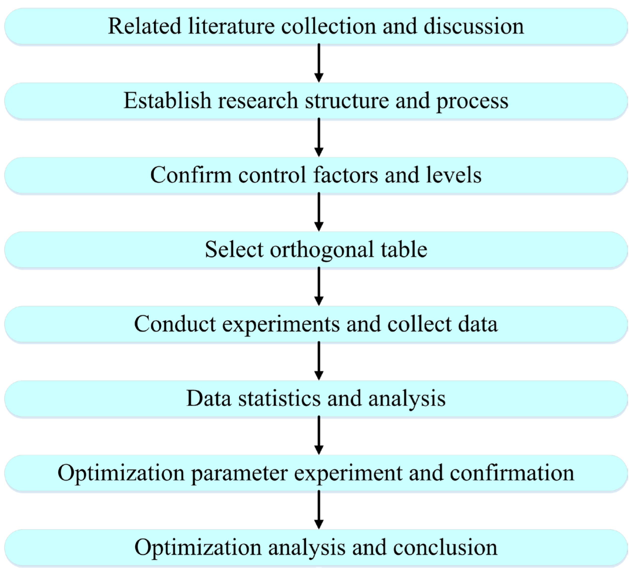
2. Material and Methods

2.1. Experimental Method

In general, most of the research methods on thin film quality adopt the method of trial and error, that is, to calculate the optimal parameters with a single-factor multi-level design method, but it is a waste of time and cost. If the optimal level of each factor is only listed as a combination parameter without considering the interaction between the factors, the result may not be optimal. Therefore, the Taguchi method can be used to improve thin film quality because it is an efficient and cost-effective quality engineering method. Experiments are used to carry out systematic parameter optimization design without difficult statistics, focusing on its practical applicability. In this work, the Taguchi method, combined with the electron-beam evaporation and ion-assisted deposition methods, was used to produce a ZrN thin film with low residual stress, a high refractive index, and minimum surface roughness. A UV/VIS/NIR spectrometer (Shimadzu UV2600i, Nakagyo Ku, Kyoto, Japan) was used to measure the refractive index and extinction coefficient of the thin films, and the envelope method was used to analyze the transmission spectrum [18,19]. The refractive index (n), extinction coefficient (k), and physical thickness of the thin film (tf) can be obtained from Equations (1)–(7), respectively.
n ( λ ) = N ( λ ) + N 2 ( λ ) n S 2 ( λ )
and
N ( λ ) = 2 n S T M ( λ ) T m ( λ ) T M ( λ ) T m ( λ ) + n S 2 ( λ ) + 1 2
n S ( λ ) = 1 T S ( λ ) + 1 T S 2 ( λ ) 1 1 2
The extinction coefficient is defined as
k ( λ ) = λ 4 π α ( λ )
where T M ( λ ) is the maximum value of the transmittance, the T m ( λ ) minimum value of the transmittance, ns(λ) is the refractive index of the substrate, and the undetermined parameters are defined as follows:
α ( λ ) = E m ( λ ) E m 2 ( λ ) n ( λ ) 1 3 n 2 ( λ ) n S 4 ( λ ) n ( λ ) 1 n 2 ( λ ) n S 2 ( λ )
E m ( λ ) = 8 n 2 ( λ ) n S T M + n 2 ( λ ) 1 n 2 ( λ ) n S 2 ( λ )
The physical thickness of the thin film can be obtained by the following formula:
t f = λ 1 λ 2 2 λ 1 n 2 λ 2 n 1
In the above Equation (7), λ 1 and λ 2 are two adjacent maxima or minima, and n 1 and n 2 are the corresponding refractive indices of λ 1 and λ 2 .
The surface roughness of the ZrN thin film is determined by a homemade Linnik microscopic interferometer. The residual stress in the thin films is measured by a Twyman–Green interferometer with a fast Fourier transform method. Finally, the measured data are entered into Minitab software to analyze the thin film’s performance. Using the signal-to-noise ratio (S/N) and its effect diagram, the main factors and levels affecting the characteristics can be found. The optimized process parameters were obtained through validation experiments. After obtaining the optimal process parameters, the polynomial regression of RSM in Minitab can be used to derive the single-objective and multi-objective optimization values. The ZrN thin film deposited on the B270 glass can achieve a low extinction coefficient and high refractive index at the same time. The optimum combination of surface roughness and residual stress can be obtained [20,21].

2.2. Factor and Level Setting

After reviewing the related literature, it was found that detailed parameters such as the equipment specifications, coating parameters, and experimental method have been studied in the literature. Therefore, we first use a low-resolution screening test and conduct test experiments with actual coating equipment to determine the significant control factors.
When conducting screening experiments, we observed the effect of deposition time on film thickness and analyzed in detail the effect of nitrogen flow rate on the properties of ZrN thin films. Increasing the nitrogen flow rate will lead to an increase in the residual compressive stress, a decrease in the extinction coefficient, a decrease in the surface roughness of the film, and a decrease in the film thickness. In addition, there may be a difference in the density of the ZrN thin film, resulting in a difference between the material density input by the quartz monitor and the actual material density. Therefore, deposition time is an important factor in controlling film thickness.
When the substrate temperature is 150 °C, the deposition of the thin film can effectively form a firm bond with the substrate and avoid peeling off. Adjusting the deposition temperature will affect the deposition rate, so it is an important factor. According to actual experiments and literature review, the nitrogen flow rate has a close interaction with the vacuum pressure, and it affects the thin film properties [22], so adjusting the nitrogen flow rate is also an important factor. In summary, we used the Taguchi method to determine the critical factors affecting the characteristics of electron-beam-deposited ZrN thin films, such as N2 flow rate, substrate temperature, and deposition time.
After passing the above screening test, the experimental factors are N2 flow rate, deposition time, and substrate temperature, as the three main process parameters, with three levels for each factor, as shown in Table 1. Select the orthogonal array of L9 (33) and replace the factors and levels in the orthogonal table, as shown in Table 2, as the configuration of research conditions because each measurement result will have some errors. Therefore, each group of process parameters is combined with the deposition of three B270 glass substrates for experiments to measure the surface roughness, residual stress, and refractive index of each coating experiment.

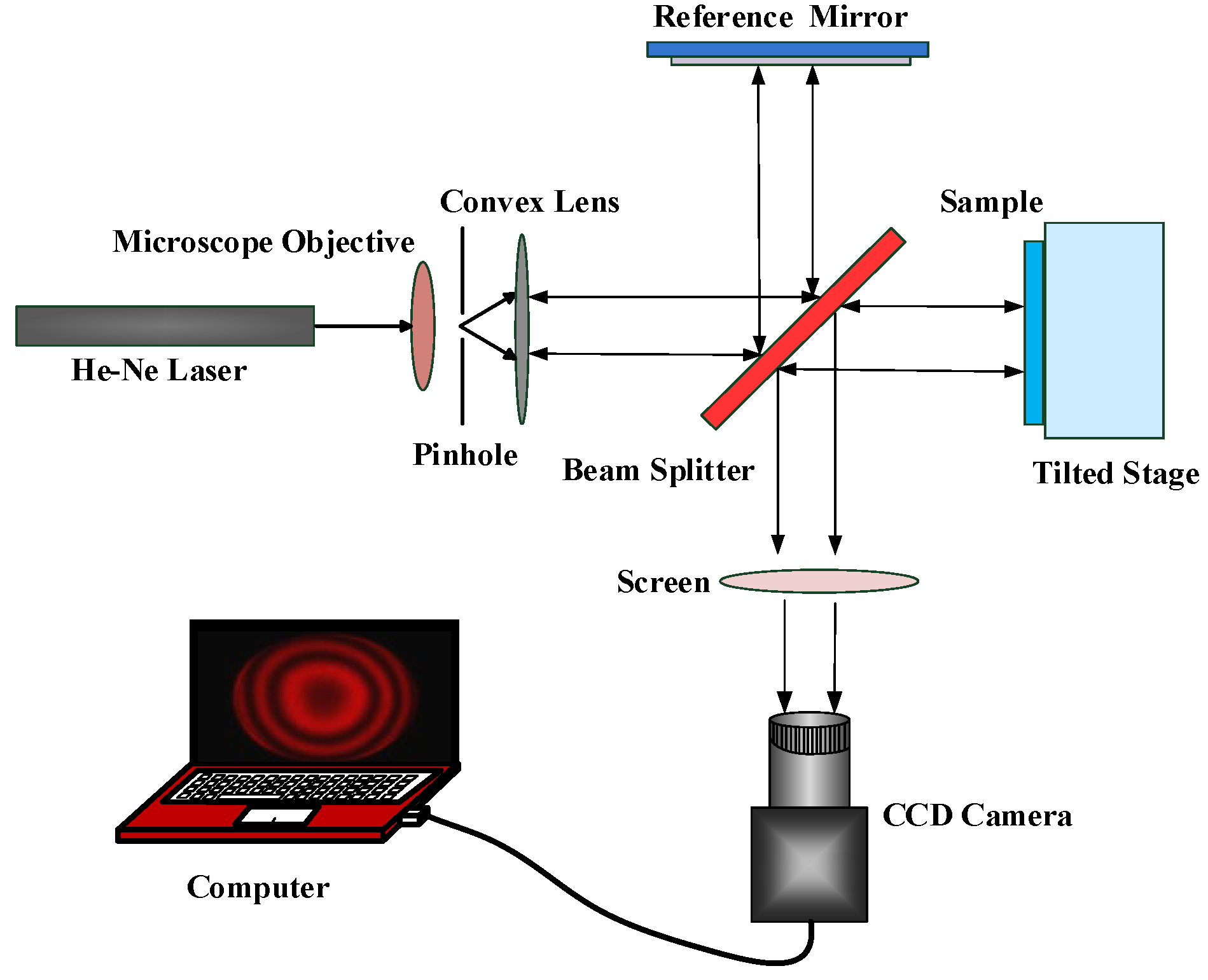
2.3. Experimental Setup

In this study, we used an electron-beam gun evaporation system with an ion beam deposition technique to prepare ZrN thin films. The vacuum chamber of the evaporation system is made of high-temperature-resistant materials such as stainless steel. In the evaporation process, we put the material to be evaporated into a crucible made of high-melting-point metal, and then melt and evaporate it by electron-beam heating. The substrate temperature is also very important and can ensure that the evaporated atoms have enough energy to move uniformly on the surface of the substrate, thereby forming a uniform film. Therefore, we need to precisely control the substrate temperature to ensure that the quality and performance of the thin film meet the requirements [23,24].
The electron-beam evaporation system (SGC-22SA, Showa Shinku, Sagamihara, Japan) combined with a Kaufman ion-assisted deposition (Mark II, Veeco, New York, NY, USA) was used in this study. We used four different pumps, including an oil rotary pump and a mechanical booster pump, for preliminary vacuum extraction, these two pumps can quickly extract the gas out of the system and reduce the pressure of the system. At the same time, in order to achieve a high vacuum, we also used a diffusion pump and a cryo pump. The maximum output power of the electron gun is 10 kW, the voltage is 10 kV, and the current is 1 A. The anode current of the ion source for ion-assisted deposition is 0.5–10 A, the anode voltage is 80–300 V, the ion energy is 50–200 eV, and the diffusion angle is 60 degrees. We deposited ZrN thin films on 1 inch diameter B270 glass and 2-inch silicon wafer substrates. All substrate surfaces must be plasma-treated prior to coating. For evaporated ZrN thin films using ion-assisted deposition, the source of nitrogen is typically a nitrogen-containing gas introduced into the deposition chamber during the coating process. The ion-assisted deposition (IAD) technique is used to enhance the properties of the deposited thin films by bombarding the growing film with high-energy ions. During the thin film deposition process, the chamber working pressure was approximately 1 × 10⁻² Pa. Pure argon and nitrogen (99.999%) gases were used in the deposition process. Thin films were deposited on glass substrates and silicon wafers by electron-beam evaporation of zirconium nitride (99.9% purity) at a deposition rate of 0.3–0.4 nm/s. Simultaneously, the substrates were heated to a growth temperature of 150 °C. The characteristics of ZrN films (bright gold in color) were produced by irradiating the growing film with 3 kW of Ar+ ions from a Kaufman ion source. The film thickness was detected by a quartz crystal thickness monitor (CRTM-6000M, ULVAC, Chigasaki, Kanagawa, Japan).
For the measurement and analysis of the ZrN thin films. The optical transmittance of thin films was measured by using a high-precision spectrophotometer (UV-2600i, Shimadzu, Nakagyo Ku, Kyoto, Japan). From the spectral data, we can calculate the optical properties of ZrN thin films such as the refractive index and extinction coefficient (i.e., optical constants). By comparing the spectral curves of the substrate and the thin film, we can evaluate the optical properties and quality of thin films. In addition, optical constants and film thickness can be verified by ellipsometry.
We used a homemade Linnik microscopic interferometer to evaluate the roughness of the thin film surface. For detailed information about the hardware structure, readers can refer to our previously published papers [25,26]. The light source uses a He-Ne laser. The laser beam becomes parallel light through the appropriate configuration of the spatial filter and collimating lens, and the influence of the diffraction effect is reduced as much as possible. Such a configuration enables highly parallel and stable beams, making it useful in laboratory and industrial applications. A cube beam splitter splits the light into two parallel beams of equal intensity, one passing through the microscope objective. After passing through the objective lens, it is directed to the surface of the thin film sample to be tested, and one is directed to the reference plate and passes through the microscope objective. At this time, the two beams reflected by the beam splitter overlap to produce interference fringes, and the CCD is used to take images and capture the interference fringes for data analysis.
In this study, a homemade Twyman–Green interferometer combined with the fast Fourier transform method [27,28] was used to measure the residual stress of the thin films [29,30], as shown in Figure 2. In the residual stress measurement, a He-Ne laser was used together with a micro-objective lens and a pinhole to generate a point source. The beam passes through a collimating lens to form a plane wavefront. A beam splitter splits the amplitude of the wavefront, producing reflected and transmitted beams. After these beams pass through the reference mirror (flatness λ/20) and the substrate to be tested, two reflected beams are recombined by a beam splitter to form an interference pattern, and finally directed to a digital CCD camera for interference pattern recording. Residual stress in thin films can be calculated by using a self-developed stress analysis program [31,32]. Precisely, by measuring the radius of the curvature difference between the substrates before and after film deposition and assuming that the residual stress is isotropic, it was deduced that the residual stress in the thin film has a proportional relationship to the deformation of the substrate. To further calculate the residual stress value in the film, we can use the modified Stoney formula [33]. The formulation is based on the geometric and elastic properties of thin film and substrate and takes into account the interfacial stress between the film and substrate.

3. Results and Discussion

3.1. Taguchi Method

In this study, the Taguchi experimental design method was applied to the electron-beam evaporation coating process to optimize the process parameters. The residual stress, refractive index, and surface roughness of the test specimens produced under the combination of nitrogen flow, substrate temperature, and deposition time with different parameters are measured. According to Taguchi’s response analysis, the influence of each process parameter can be analyzed. Furthermore, we can find the best combination of process parameters. There are nine groups in the experiment. According to the experimental results shown in Table 3, there is a certain error in each measurement. In order to improve the reliability of the measurement, we conducted three experiments combining each set of device parameters with three pieces of B270 circular glass substrates. We measured parameters such as residual stress, reflectivity, and surface roughness. By calculating the median of the measured data, we determined the film results and took the arithmetic mean as the result of the experimental combination. This reduces measurement errors and increases the reliability of experimental results.
In Taguchi quality engineering, there are three standard types of computational loss functions, namely “nominal-the-better”, “larger-the-better”, and “smaller-the-better”. These loss functions are used to evaluate the performance of a system or process and select an appropriate function according to its optimization goal. In order to obtain stable quality characteristics after film deposition, the value of the signal-to-noise ratio (S/N) was used as a comparison difference. The higher the refractive index, the better; the lower the surface roughness, the better; the lower the residual stress is the better for ZrN thin films; the negative sign of the value indicates its directionality. The mathematical expression is that compressive stress is negative and tensile stress is positive [34,35].
Since there are many combinations of control factors, this study uses Minitab analysis software to calculate signal-to-noise ratios and predict the best combination of solutions. After the Minitab calculation, the best combination of parameters for the refractive index is shown in Table 4. The asterisks and minuses in Table 4, Table 5 and Table 6 indicate significant and negative values, respectively. According to the experimental data and prediction results, it can be concluded that under the conditions of the N2 flow rate of 14 sccm, deposition time of 60 min, and substrate temperature of 150 °C, the signal-to-noise ratio of the predicted ZrN thin film is 7.252. This indicates that under this set of parameters, the resulting film has a good balance between signal and noise and is of good quality. In addition, by comparing the results under different parameter combinations, according to our findings, at an N2 flow rate of 14 sccm, with a substrate temperature of 130 °C and a deposition time of 60 min, we predict a signal-to-noise ratio of 4.757, showing better performance for residual stress. Table 5 shows the smaller the residual stress is the better. Furthermore, in terms of surface roughness, the predicted signal-to-noise ratio is −2.499, and its optimal parameter combination is the N2 flow rate of 18 sccm, substrate temperature of 130 °C, and deposition time of 80 min, showing a relatively low surface roughness. Table 6 shows the smaller is better for surface roughness. Based on the above results, we can conclude that various properties of ZrN thin films can be optimized and controlled by adjusting parameters such as N2 flow rate, substrate temperature, and deposition time. These results provide the opportunity to further improve film properties and address specific applications.
Through the Taguchi method to analyze the S/N ratio effect table of the experiment of zirconium nitride thin film, it can be known that the important factors affecting the refractive index are in the order of A N2 flow rate > B deposition time > C substrate temperature, and the combination of “refractive index” quality characteristic parameters is pursued for A1B2C3. The important factors affecting the residual stress are B deposition time > A N2 flow rate > C substrate temperature, and the combination of “residual stress” quality characteristic parameters is A1B2C1. The important factors influencing the surface roughness are in the order of B deposition time > C substrate temperature > A N2 flow rate, and the combination of “surface roughness” quality characteristics is A3B3C1.

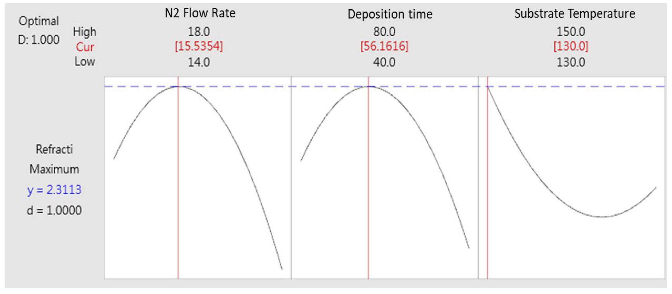
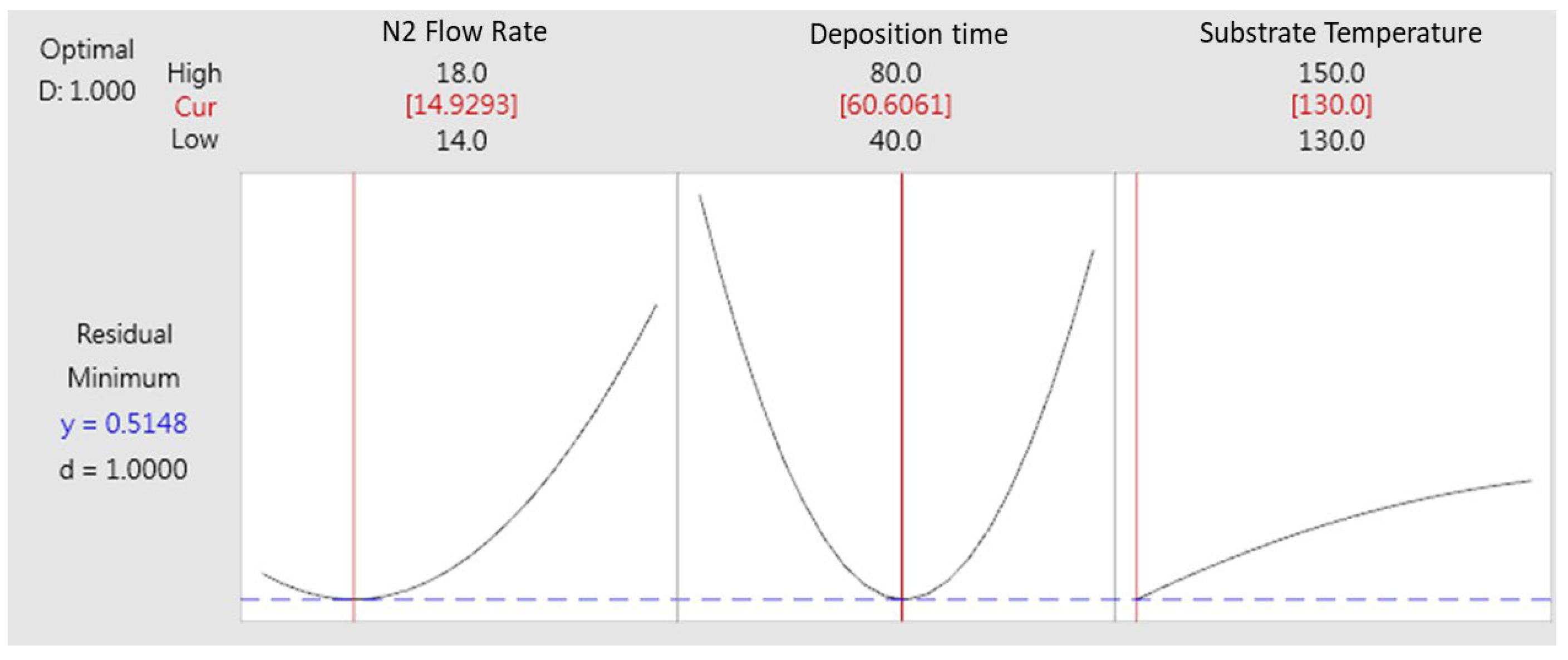
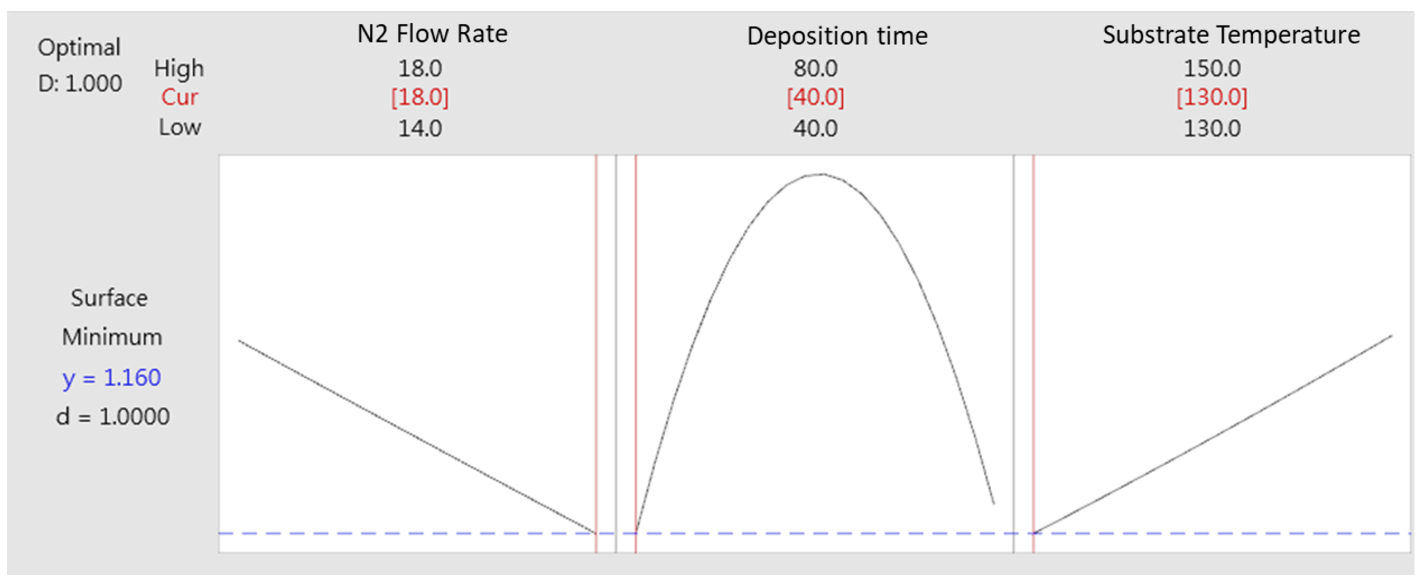
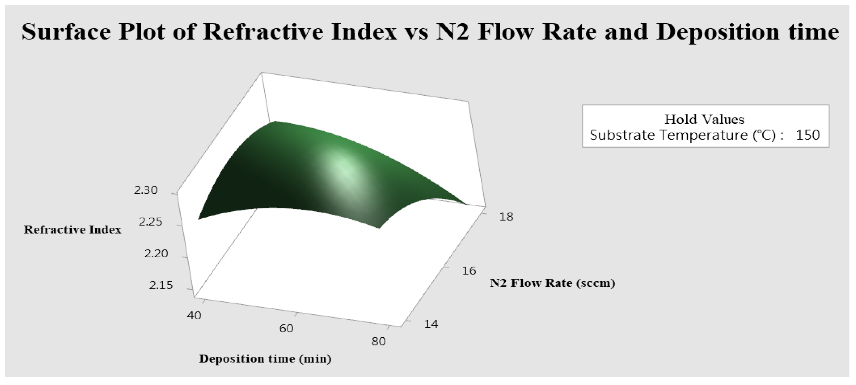
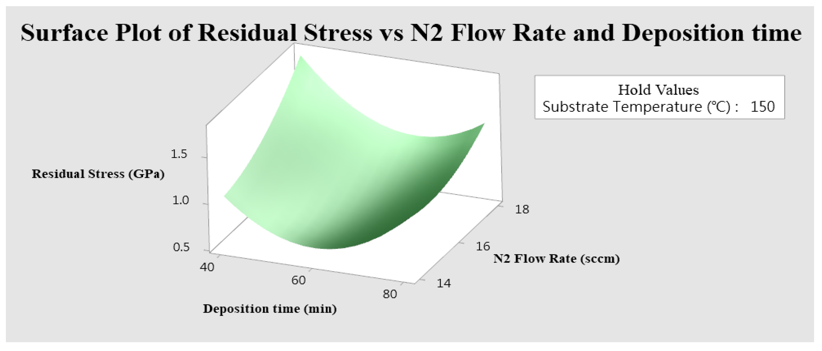
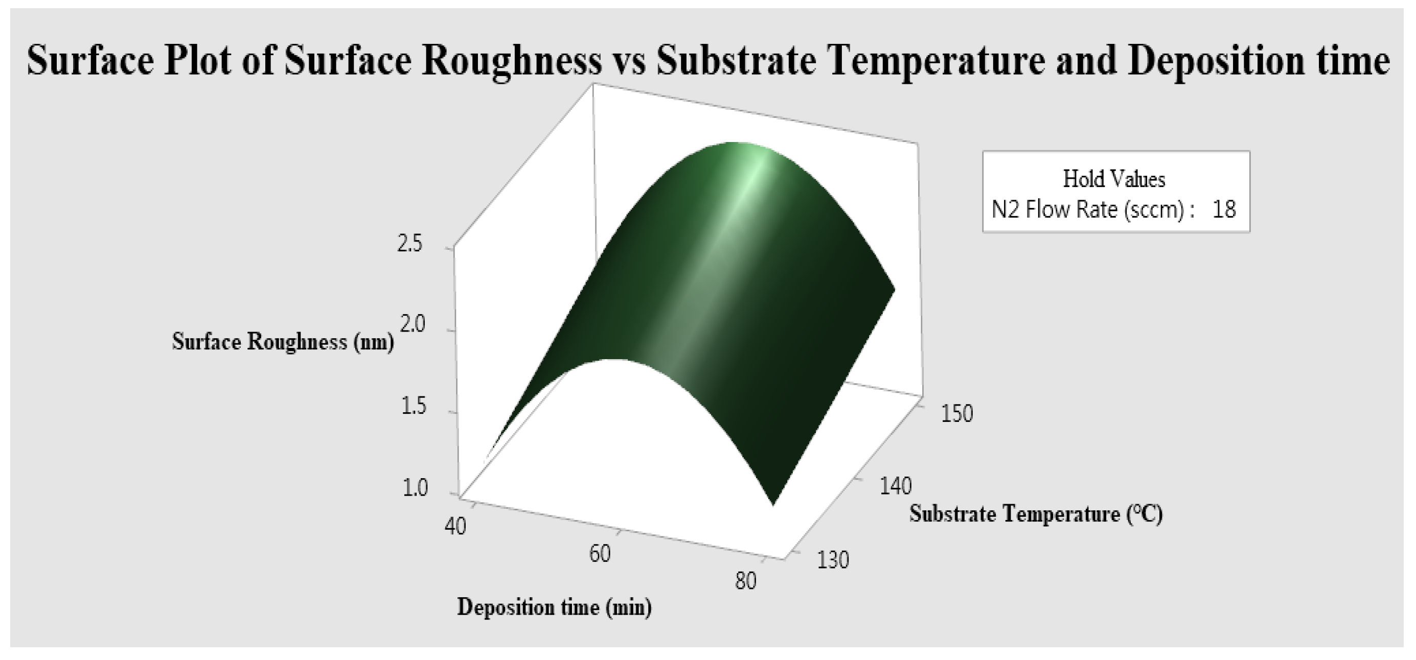
3.2. Response Surface Method

The response surface method uses the data obtained from the experimental results to evaluate the effect of each factor, find the relationship between the variables and the response value, confirm the accuracy and reliability of the experiment, and estimate the influence of the parameters on the target value.
The factors affecting the refractive index, surface roughness, and residual stress characteristics of the ZrN films were analyzed by the Taguchi method, but more accurate coating parameters could not be analyzed, and many factors affect the characteristics of ZrN films. Therefore, to optimize the experimental data, Minitab statistical software was used for response surface methodology analysis. This polynomial equation can predict and optimize the response value of the refractive index quality characteristics. Response surface analysis and prediction can obtain response surface optimization graphs, as shown in Figure 3, Figure 4 and Figure 5, respectively. The three-dimensional response surface graphs are shown in Figure 6, Figure 7 and Figure 8. Using the response surface approach, we can formulate a model to predict thin film properties as the following equations.
n(A,B,C) = 2.094 + 0.3114 A + 0.01873 B − 0.03773 C − 0.006708 A2 − 0.000063 B2 + 0.000157 C2 − 0.000750 A × B − 0.000467 A × C
σ(A,B,C) = 9.001 − 1.169 A − 0.08816 B + 0.03388 C + 0.03608 A2 + 0.001092 B2 − 0.000208 C2 − 0.002983 A × B + 0.002100 A × C
R(A,B,C) = −0.09000 − 0.3692 A + 0.2272 B − 0.02967 C + 0.000417 A2 − 0.001917 B2 + 0.000067 C2 + 0.000250 A × B + 0.001833 A × C
where n is the refractive index, σ is residual stress and R stands for surface roughness. A is nitrogen flow, B is deposition time, and C is substrate temperature.
By optimizing the equations of residual stress, refractive index, and surface roughness, we can determine the combination of parameters and their corresponding values that achieve the best balance among multiple objectives. We obtained the parameter combinations with the best quality properties using a response surface approach for multi-objective prediction. These optimized parameters can ensure the excellent performance of ZrN thin films deposited on B270 glass, thus providing solutions for related applications, as shown in Table 7. Compared with single-objective optimization, the quality characteristic value of multi-objective optimization is slightly poor, but in practice, the performance of multi-objective optimization is more in line with practical needs.

4. Conclusions

In this study, electron-beam evaporation combined with the IAD technique was used to prepare ZrN thin films. The Taguchi method and plasma surface treatment were used to optimize the deposition process and reduce the surface roughness of the ZrN thin films. The target characteristics of refractive index, residual stress, and surface roughness after ZrN thin film deposition were discussed. The ion-assisted electron-beam evaporation process is an important technique that affects the properties of ZrN thin films.
The results can be summarized as follows:
(a)
By applying the Taguchi method, we were able to obtain optimal design parameters to achieve the best performance of ZrN thin films in terms of refractive index, residual stress, and surface roughness. Through the experimental design and statistical analysis based on the Taguchi method, we systematically investigated various factors on the ZrN thin film properties and found the optimal process conditions. This allowed us to more efficiently optimize the process parameters to achieve the desired thin film performance targets. According to the response surface methodology, polynomial equations for predicting residual stress, surface roughness, and refractive index can be obtained.
(b)
By applying the response surface method, we successfully performed multi-objective optimization to obtain ZrN thin films with high refractive index, low residual stress, and low surface roughness. During the optimization process, we adjusted the parameters of the optimization factors so that the N2 flow rate was 15.37 sccm, the deposition time was 80 min, and the substrate temperature was 130 °C.
(c)
Through systematic experiments and statistical analysis, we were able to determine the optimal combination of parameters to achieve the best properties of the ZrN thin film. This study provides essential guidance for the preparation of ZrN thin films and also demonstrates the application of the response surface method in multi-objective optimization.
(d)
The Taguchi method and the response surface method can be used to find the maximum or minimum value of a specific parameter characteristic for single-objective quality characteristics, while the response surface method for multi-objective quality characteristics can consider a variety of factors and find the corresponding optimized parameters.

Author Contributions

Conceptualization, C.-L.T. and C.-Y.C.; methodology, C.-L.T.; writing—review and editing, C.-L.T. and C.-Y.C.; validation, C.-L.T. and C.-Y.C.; formal analysis, C.-L.T. and S.-C.L., data curation, C.-Y.C. and S.-C.L. All authors have read and agreed to the published version of the manuscript.

Funding

The authors are grateful for the financial support of the Taiwan Ministry of Education for this research project. This research was supported in part by the National Science and Technology Council, under project number MOST 111-2622-E-035-003. This study was also supported by Feng Chia University (Contract No. 22H00319).

Institutional Review Board Statement

Not applicable.

Informed Consent Statement

Not applicable.

Data Availability Statement

Not applicable.

Acknowledgments

Authors are grateful to the Precision Instrument Support Center of Feng Chia University for providing SPM analytical facilities.

Conflicts of Interest

The authors declare no conflict of interest.

References

  1. Budke, E.; Krempel-Hesse, J.; Maidhof, H.; Schüssler, H. Decorative hard coatings with improved corrosion resistance. Surf. Coat. Technol. 1999, 112, 108–113. [Google Scholar] [CrossRef]
  2. Mubarak, A.; Hamzah, E.B.; Mohd Toff, M.R.H.; Hashim, A.H.B. The effect of nitrogen gas flow rate on the properties of coated high-speed steel (HSS) using cathodic arc evaporation physical vapor deposition (PVD) technique. Surf. Rev. Lett. 2005, 12, 631–643. [Google Scholar] [CrossRef]
  3. Mitterer, C.; Mayrhofer, P.; Waldhauser, W.; Kelesoglu, E.; Losbichler, P. The influence of the ion bombardment on the optical properties of TiNx and ZrNx coatings. Surf. Coat. Technol. 1988, 108–109, 230–235. [Google Scholar] [CrossRef]
  4. Liu, C.P.; Yang, H.G. The Texture and Electrical Properties of Zr and ZrNx Thin Films Deposited by DC Sputtering. Mat. Res. Soc. Symp. Proc. 2002, 721, 49. [Google Scholar] [CrossRef]
  5. Lide, D. CRC Handbook of Chemistry and Physics: A Ready-Reference Book of Chemical and Physical Data; CRC: Boca Raton, FL, USA, 2009. [Google Scholar]
  6. Mei, A.B.; Howe, B.M.; Zhang, C.; Sardela, M.; Eckstein, J.N.; Hultman, L.; Rockett, A.; Petrov, I.; Greene, J.E. Physical properties of epitaxial ZrN/MgO(001) layers grown by reactive magnetron sputtering. J. Vac. Sci. Technol. A 2013, 31, 061516. [Google Scholar] [CrossRef]
  7. Phadke, M. Quality Engineering Using Robust Design; Prentice Hall: Englewood Cliffs, NJ, USA, 1989. [Google Scholar]
  8. Musil, J.; Karvánková, P.; Kasl, J. Hard and superhard Zr-Ni-N nanocomposite films. Surf. Coat. Technol. 2001, 139, 101–109. [Google Scholar] [CrossRef]
  9. Kuznetsova, K.; Lapitskaya, V.; Khabarava, A.; Chizhik, S.; Warcholinski, B.; Gilewicz, A. The influence of nitrogen on the morphology of ZrN coatings deposited by magnetron sputtering. Appl. Surf. Sci. 2020, 522, 146508. [Google Scholar] [CrossRef]
  10. Dehnad, K. Quality Control, Robust Design, and the Taguchi Method; Springer: Berlin/Heidelberg, Germany, 2012. [Google Scholar]
  11. Barker, T.B. Engineering Quality by Design; Marcel Dekker: New York, NY, USA, 1990. [Google Scholar]
  12. Hinna, M.; Hartiti, B.; Gouya, A.; Labrim, H.; Fadili, S.; Tahri, M.; Belfhailli, A.; Siadat, M.; Thévenin, P. Synthesis of ITO thin films by Spray pyrolysis based on Taguchi design. Materialstoday 2022, 66, 447–455. [Google Scholar] [CrossRef]
  13. Rajath, H.G.; Byregowda, H.V.; Siddesh Kumar, N.M. Optimization of ZnO Thin Films using Sol-Gel Dip Coating by Taguchi Method. Eur. Chem. Bull. 2023, 12, 670–681. [Google Scholar]
  14. Puźniak, M.; Gajewski, W.; Seweryn, A.; Klepka, M.T.; Witkowski, B.S.; Godlewski, M.; Mroczyński, R. Studies of Electrical Parameters and Thermal Stability of HiPIMS Hafnium Oxynitride (HfOxNy) Thin Films. Materials 2023, 16, 2539. [Google Scholar] [CrossRef]
  15. Wu, C.Y.; Chen, J.H.; Kuo, C.G.; Twu, M.J.; Peng, S.W.; Hsu, C.Y. Effects of deposition parameters on the structure and properties of ZrN, WN and ZrWN films. Bull. Mater. Sci. 2019, 42, 38. [Google Scholar] [CrossRef] [Green Version]
  16. Doubi, Y.; Hartiti, B.; Siadat, M.; Labrim, H.; Fadili, S.; Stitou, M.; Tahri, M.; Belfhaili, A.; Thevenin, P.; Losson, E. Optimization with Taguchi approach to prepare pure TiO2 thin films for Future Gas Sensor Application. J. Electron. Mater. 2022, 51, 3671–3683. [Google Scholar] [CrossRef]
  17. Maghsoodloo, S.; Ozdemir, G.; Jordan, V.; Huang, C. Strengths and limitations of Taguchi’s contributions to quality, manufacturing, and process engineering. J. Manuf. Syst. 2004, 23, 73–126. [Google Scholar] [CrossRef]
  18. Manifacier, J.C.; Gasiot, J.; Fillard, J.P. A simple method for the determination of the optical constants n, k and the thickness of a weakly absorbing thin film. J. Phys. E Sci. Instrum. 1976, 9, 1002–1004. [Google Scholar] [CrossRef]
  19. Swanepoel, R. Determination of the thickness and optical constants of amorphous silicon. J. Phys. E Sci. Instrum. 1983, 16, 1214–1218. [Google Scholar] [CrossRef] [Green Version]
  20. Nadji, S.N.; Lequime, M.; Begou, T.; Koc, C.; Grèzes-Besset, C.; Lumeau, J. In-situ interferometric monitoring of optical coatings. Opt. Express 2020, 28, 22012–22026. [Google Scholar] [CrossRef]
  21. Tien, C. Biaxial stresses, surface roughness and microstructures in evaporated TiO2 films with different deposition geometries. Appl. Surf. Sci. 2009, 256, 870–875. [Google Scholar] [CrossRef]
  22. Smith, D.L. Thin-Film Deposition: Principles and Practice; McGraw-Hill: New York, NY, USA, 1995. [Google Scholar]
  23. Sree Harsha, K.S. Principles of Physical Vapor Deposition of Thin Films; Elsevier: Great Britain, UK, 2006. [Google Scholar]
  24. Mavukkandy, M.O.; McBride, S.A.; Warsinger, D.M.; Dizge, N.; Hasan, S.W.; Arafat, H.A. Thin film deposition techniques for polymeric membranes—A review. J. Membr. Sci. 2020, 610, 118258. [Google Scholar] [CrossRef]
  25. Tien, C.L.; Yu, K.C.; Tsai, T.Y.; Lin, C.S.; Li, C.Y. Measurement of surface roughness of thin films by a hybrid interference microscope with different phase algorithms. Appl. Opt. 2014, 53, H213. [Google Scholar] [CrossRef]
  26. Tien, C.L.; Lin, T.W.; Yu, K.C.; Tsai, T.Y.; Shih, H.F. Evaluation of electrical, mechanical properties, and surface roughness of dc sputtering nickel-iron thin films. IEEE Trans. Magn. 2014, 50, 2005304. [Google Scholar] [CrossRef]
  27. Takeda, M.; Ina, H.; Kobayashi, S. Fourier-transform method of fringe-pattern analysis for computer-based topography and interferometry. Appl. Opt. 1982, 72, 156–160. [Google Scholar] [CrossRef]
  28. Takeda, M.; Mutoh, K. Fourier transform profilometry for the automatic measurement of 3-D object shapes. Appl. Opt. 1983, 22, 3977–3982. [Google Scholar] [CrossRef] [PubMed]
  29. Tien, C.L.; Zeng, H.D. Measuring residual stress of anisotropic thin film by fast Fourier transform. Opt. Express 2010, 18, 16594–16600. [Google Scholar] [CrossRef]
  30. Tien, C.L.; Lin, T.W.; Jyu, S.S.; Tseng, H.D.; Lin, C.S.; Liu, M.C. The measurement of anisotropic stress in obliquely-deposited thin films by fast Fourier transform and Gaussian filter. Phys. Procedia 2011, 19, 21–26. [Google Scholar] [CrossRef]
  31. Tien, C.L.; Lin, T.W. Measurement of stress anisotropy in magnetic thin films by fast Fourier transform method. IEEE Trans. Magn. 2011, 47, 3905–3908. [Google Scholar] [CrossRef]
  32. Tien, C.L.; Lee, C.C.; Tsai, Y.L.; Sun, W.S. Determination of the mechanical properties of thin films by digital phase shifting interferometry. Opt. Commun. 2001, 198, 325–331. [Google Scholar] [CrossRef]
  33. Brenner, A.; Senderoff, S. Calculation of stress in electrodeposits from the curvature of a plated strip. J. Res. Natl. Bur. Stand. 1949, 42, 105–123. [Google Scholar] [CrossRef]
  34. Begou, T.; Lumeau, J. Accurate analysis of mechanical stress in dielectric multilayers. Opt. Lett. 2017, 42, 3217–3220. [Google Scholar] [CrossRef]
  35. Begou, T.; Lemarchand, F.; Lemarquis, F.; Moreau, A.; Lumeau, J. High-performance thin-film optical filters with stress compensation. J. Opt. Soc. Am. A 2019, 36, C113–C121. [Google Scholar] [CrossRef] [Green Version]
Figure 1. Flow chart of this work.
Plasma 06 00033 g001
Figure 2. Schematic diagram of Twyman–Green interferometer.
Plasma 06 00033 g002
Figure 3. Optimization graph of the refractive index equation.
Plasma 06 00033 g003
Figure 4. Optimization graph of residual stress equation.
Plasma 06 00033 g004
Figure 5. Optimization graph of surface roughness equation.
Plasma 06 00033 g005
Figure 6. Surface plot of refractive index versus N2 flow rate and deposition time.
Plasma 06 00033 g006
Figure 7. Surface plot of residual stress versus N2 flow rate and deposition time.
Plasma 06 00033 g007
Figure 8. Surface plot of surface roughness versus substrate temperature and deposition time.
Plasma 06 00033 g008
Table 1. Control factors with different levels.
Experimental Control FactorsLevels of Factor
123
N2 flow rate (sccm)141618
Deposition time (min)406080
Substrate temperature (°C)130140150
Table 2. Orthogonal array (L9(33)) for ZrN test samples.
Factory (Level)
Test NumberN2 Flow Rate
(sccm)
Deposition Time
(min)
Substrate
Temperature (°C)
114 (1)40 (1)130 (1)
214 (1)60 (2)140 (2)
314 (1)80 (3)150 (3)
416 (2)40 (1)140 (2)
516 (2)60 (2)150 (3)
616 (2)80 (3)130 (1)
718 (3)40 (1)150 (3)
818 (3)60 (2)130 (1)
918 (3)80 (3)140 (2)
Table 3. The combination of nine coating parameters and the experimental measurement results.
Test
Number
Experimental Measurement Results
Refractive IndexSurface Roughness (nm)Residual Stress (GPa)
12.2601.590.959
22.2792.510.615
32.2791.911.103
42.2701.551.205
52.2812.530.742
62.2661.420.899
72.2391.601.782
82.2631.960.862
92.1531.441.237
Table 4. S/N ratio for larger-is-better for refractive index.
Response Table for Signal to Noise Ratios
LevelN2 Flow Rate
(sccm)
Deposition
Time (min)
Substrate
Temperature (°C)
1* 7.1307.0657.093
27.029* 7.1366.978
36.9166.974* 7.103
Delta0.2140.1620.125
Rank123
* indicates significant.
Table 5. Smaller is better for residual stress.
Response Table for Signal to Noise Ratios
LevelN2 Flow Rate
(sccm)
Deposition
Time (min)
Substrate
Temperature (°C)
1* 1.2262−2.0956* 0.8408
20.6109* 2.66730.2371
3−1.8715−0.6061−1.1124
Delta3.09774.76291.9532
Rank213
* indicates significant.
Table 6. Smaller is better for surface roughness.
Response Table for Signal to Noise Ratios
LevelN2 Flow Rate
(sccm)
Deposition
Time (min)
Substrate
Temperature (°C)
1−5.907−3.992* −4.332
2−4.996−7.317−5.011
3* −4.382* −3.976−5.943
Delta1.5243.3411.611
Rank312
* indicates significant.
Table 7. Optimization results of single- and multi-objective quality characteristics of ZrN thin film.
Optimize the TargetsQuality CharacteristicsN2 Flow Rate
(sccm)
Deposition Time (min)Substrate Temperature (°C)Results
Single-objective optimizationRefractive index15.5456.161302.283
Residual stress (GPa)14.9360.611300.611
Surface roughness (nm)18401301.33
Multi-objective optimizationRefractive Index15.37801302.278
Residual stress (GPa)0.901
Surface roughness (nm)1.481
Disclaimer/Publisher’s Note: The statements, opinions and data contained in all publications are solely those of the individual author(s) and contributor(s) and not of MDPI and/or the editor(s). MDPI and/or the editor(s) disclaim responsibility for any injury to people or property resulting from any ideas, methods, instructions or products referred to in the content.

