Article

An Efficient Method for Simulating the Temperature Distribution in Regions Containing YAG:Ce3+ Luminescence Composites of White LED

by
Quang-Khoi Nguyen
1,2,* and
Thi-Hanh-Thu Vu
1,2
1
Falculty of Physics and Engineering Physics, VNUHCM-University of Science, Ho Chi Minh City, Vietnam
2
Vietnam National University Ho Chi Minh City, Ho Chi Minh City, Vietnam
*
Author to whom correspondence should be addressed.
J. Compos. Sci. 2023, 7(7), 301; https://doi.org/10.3390/jcs7070301
Submission received: 6 July 2023 / Accepted: 14 July 2023 / Published: 22 July 2023
(This article belongs to the Special Issue Characterization and Modelling of Composites, Volume III)

Abstract

:
A thermal model was built to estimate the temperature distribution in the hemispherical packaging volume of a white LED at a steady state. Inherent heat sources appeared in the white LED when its power was measured. A simplified 3D to 2D space process that improves the model and solves the heat diffusion equation in a simpler and faster manner is presented. The finite element method was employed using MATLAB software (version R2017b) to identify the temperature distribution. The model was applied for different values of injection current, including 50 mA, 200 mA, 350 mA, and 500 mA. The influence of the injection current and thermal conductivity difference on the temperature distribution of the encapsulant, blue LED die, and substrate region was clearly observed. The results indicate that white light packaging technology should locate phosphor far from the LED die, that the thermal conductivity of the silicone–phosphor region should be improved, that heat should be dissipated for pc-WLEDs when using a high operating power, and that the injection current should be kept as moderate as possible.

1. Introduction

Solid-state lighting (SSL) has gradually been replacing incandescent light bulbs owing to its advantages, including high energy efficiency, fast response, acceptable color rendering, long lifetime, and low cost [1,2]. White light can be created in various ways, such as with dichromatic, trichromatic, and tetrachromatic approaches [3]. Among them, the dichromatic approach is widely used due to its simplicity and efficiency, in which white light is created by the combination of a blue LED die and yellow phosphor [3]. The quality of phosphor-converted white light-emitting diodes (pc-WLEDs) depends on many factors such as the blue LED die, type of yellow phosphor, packaging technology, packaging structure, and thermal management [4,5,6,7,8,9,10,11]. For better thermal management, it is not only necessary to reduce the amount of generated heat accumulated in the packaging volume, but also to know the temperature distribution characteristics [12,13,14]. In packaging technology, there are several main factors that affect the thermal characteristics of pc-WLEDs, including phosphor loss, geometry loss, weight concentration of yellow phosphor, Stoke loss, packaging structure, and the efficacy of the blue LED die [15,16,17]. The phosphor loss is caused by the limitation of the internal quantum efficiency of yellow phosphor. This is an inherent property of yellow phosphor and can be reduced by choosing a type of phosphor with high internal quantum efficiency from the datasheet of phosphor suppliers. Geometry loss is related to the extraction efficiency of white light as higher extraction efficiency reduces the absorption rate in the packaging volume and thus reduces the generated heat. The different weight concentrations of yellow phosphor can have different effects on the output power due to the backward scattering problem, thus increasing the absorption rate, leading to increasing temperature in the packaging volume. The Stoke loss is related to the wavelength difference between the excitation and reemitted wavelengths [3]. Since the type of blue LED die and phosphor material are usually established by the manufacturer, the Stoke loss can be minimized by choosing suitable types of LED and yellow phosphor so that the wavelength difference is minimal. A packaging structure with different phosphor locations not only affects the optical path length of the photon that affects the color performance of the pc-WLED, but also the temperature distribution in the packaging volume of the pc-WLED [18,19]. In the hemispherical phosphor distribution, the phosphor will is located far from the LED die region, which is a very hot region during pc-WLED operation. The efficacy of the blue LED die is related to the conversion efficiency of the injected electron to the emitted blue photon. The conversion efficiency from electrical power to optical power is 30–40%; thus, 60–70% is transformed into heat [16,17]. This process is the main factor that increases the temperature of pc-WLEDs. This heating effect is more serious when using a higher injection current or for high-power pc-WLEDs.
It is well known that temperature is one of the key factors that have a significant effect on the final output of white light in terms of CCT, CRI, luminous efficiency, lifespans, and mechanical properties [8,9,10,11]. In the field of packaging technology, a clearer understanding of the temperature distribution in packaging volume is important for better thermal management of pc-WLEDs as well as a higher quality of lighting products. The temperature problem in the pc-WLED lamp has attracted the attention of many research works. Baran et al. presented precise thermal modeling of the LED module using CFD software for determining the temperature of the junction of semiconductor light sources [12]. Fu et al. used commercial software based on the finite element method developed by COMSOL to conduct a 3D simulation of the thermal paths of the LED module to effectively evaluate its final steady state [13]. Chen et al. developed a 3D finite element model (FEM) using ANSYS to simulate the thermal performance and temperature distributions of flat-surface high-power GaN-based flip-chip light-emitting diodes [14]. Tan et al. used ANSYS software for the simulation of the temperature distribution of the encapsulated LED structure, wherein the phosphor is conformally coated onto the blue LED die, which is powered at 0.35 A [20]. Nemitz et al. conducted thermal simulations using the GPL-software packages GetDP/Gmsh (Finite Element Method, FEM), which allowed the determination of the temperature distribution in the color conversion elements of a phosphor-converted LED with good accuracy [21]. Zhang et al. based their study on finite element ICEPAK software to develop a thermal model of a high-power white LED street light that could simulate the temperature field distribution of the LED chip [22]. Chatterjee et al. presented a three-dimensional finite element model of the green LEDs grown on gallium nitride (GaN) and sapphire substrates placed on heat sinks in order to develop a better understanding of the heat transport limitations of heat sinks [23].
In this paper, we propose a simple way to simulate the temperature distribution in the packaging volume of pc-WLEDs with a hemispherical structure at a steady state. A steady-state thermal model was used to identify the temperature distribution corresponding to different injection currents. This finite element method using MATLAB software (version R2017b) is simple, fast, and efficient when estimating the spatial temperature distribution in the packaging volume of pc-WLEDs. The thermal model can be efficiently applied to the packaging geometry, which uses a hemispherical structure with a low weight concentration of yellow phosphor (e.g., <10%).

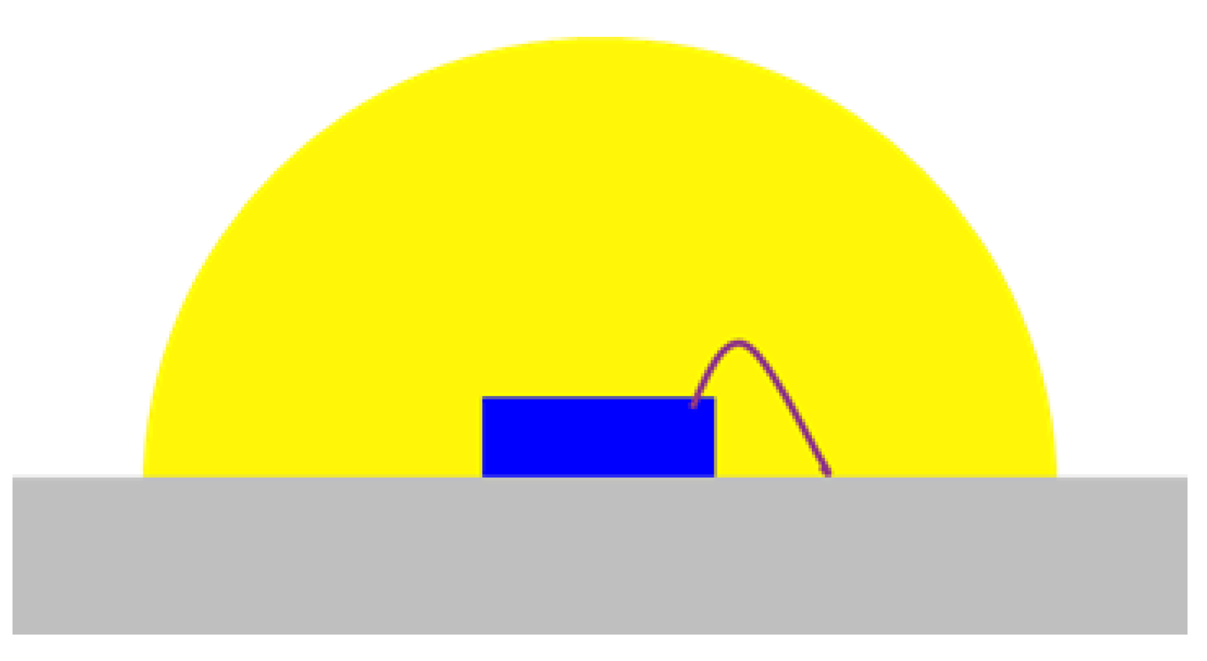
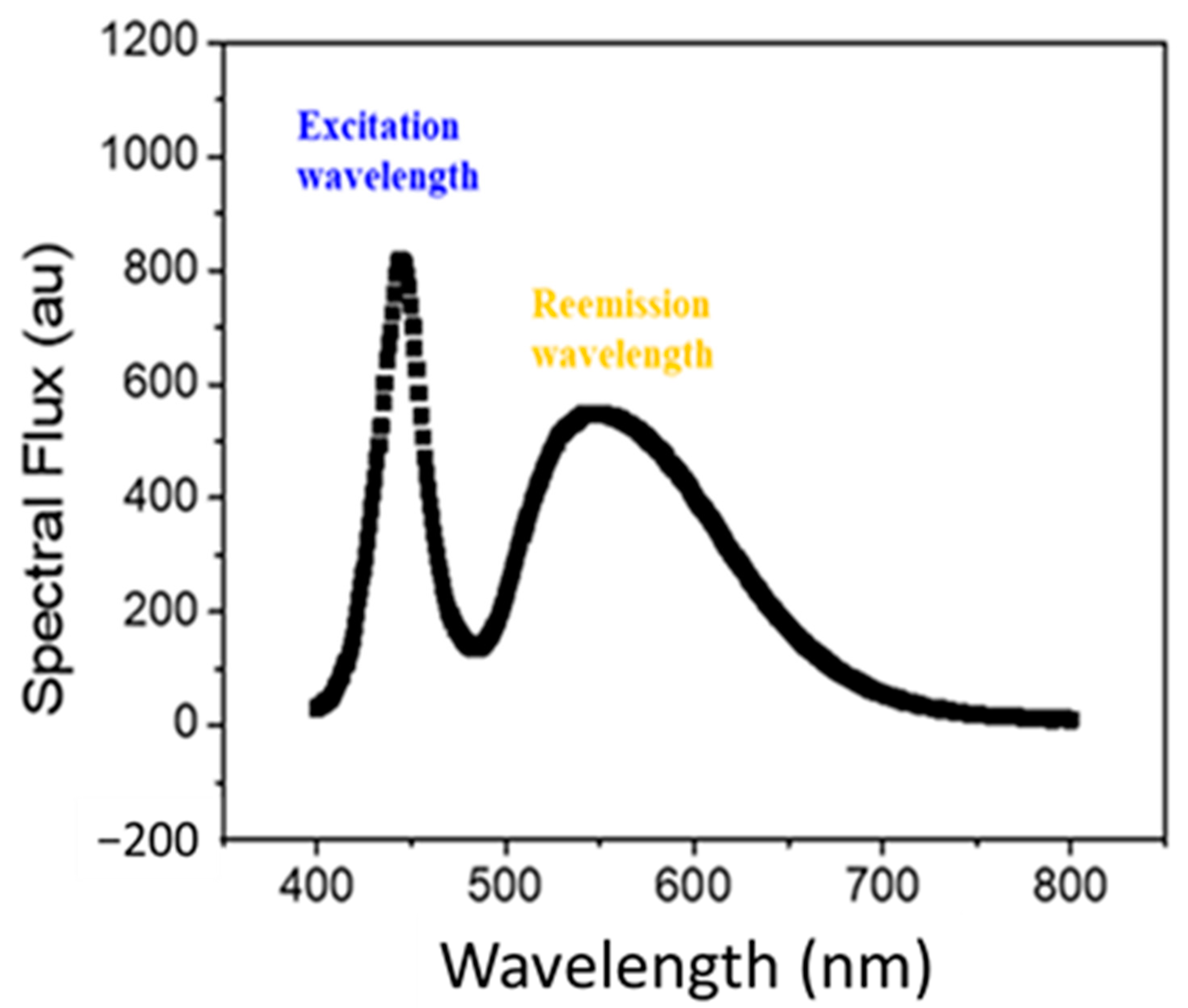
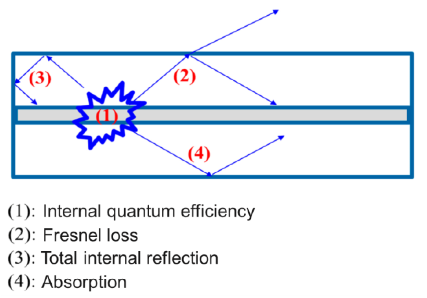
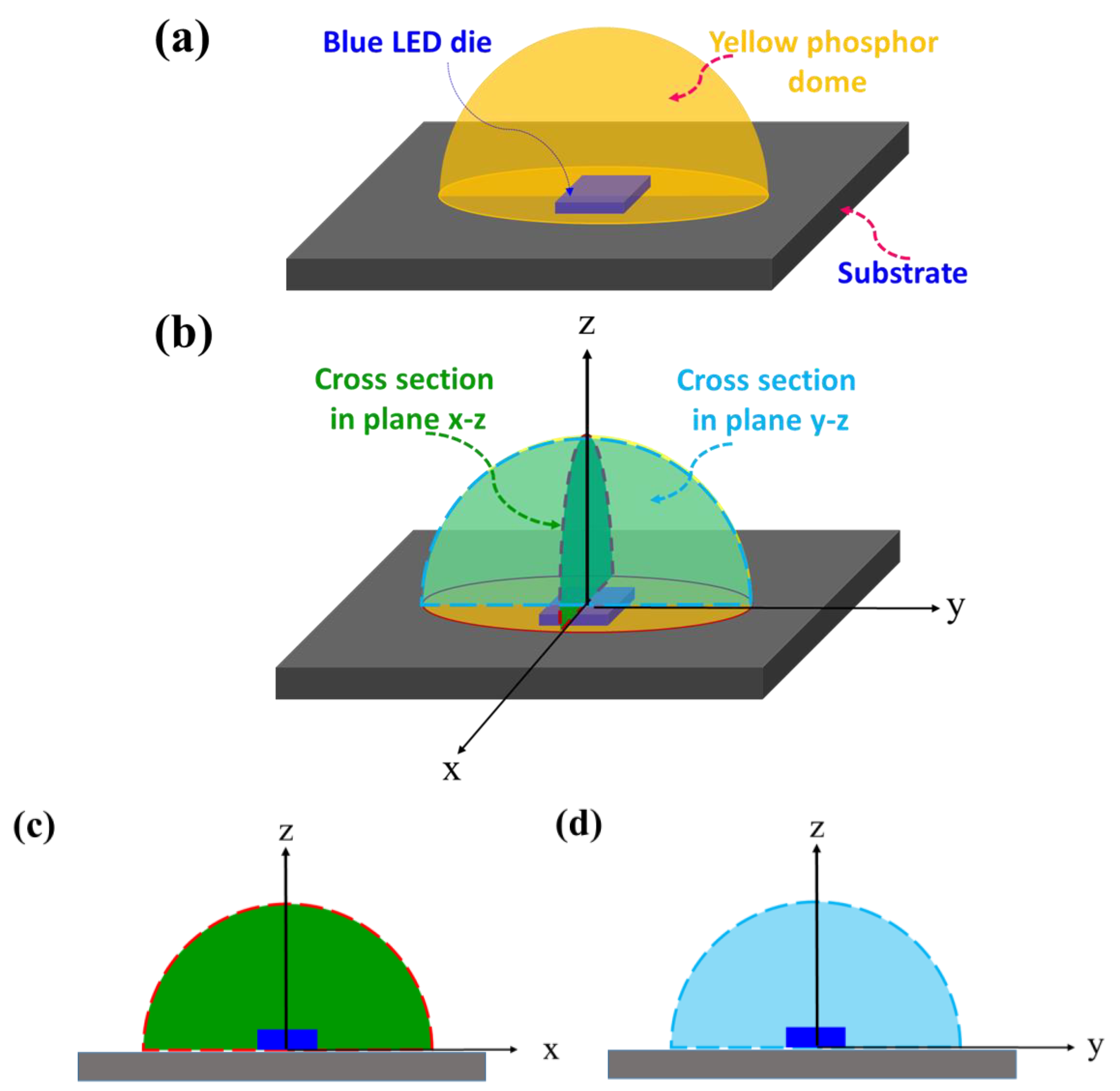
2. Two Main Heat Sources in pc-WLEDs Using a Hemispherical Silicone–Phosphor Matrix Distribution

A cross section of the hemispherical packaging structure is illustrated in Figure 1. The blue LED die is bonded on the aluminum nitride (AlN) substrate, and the gold alloy is used to connect the anode on the top LED die to the anode part on the substrate. The mixture of silicone gel and yellow phosphor is shaped as a hemisphere. There are two main sources that significantly contribute to the heat generation in the pc-WLED structure when a pc-WLED is operated.
The first heat source comes from the phosphor region. As shown in Figure 2, the peak of the blue excitation wavelength and yellow emission wavelengths are 450 nm and 550 nm, respectively. Therefore, the wavelength conversion efficiency (the ratio of the excitation wavelength to re-emission wavelength) is about 82%. Thus, about 18% of the energy from this process is converted to heat.
The second heat source is the blue LED die when the injected electrical current passes through it. There are different ways to generate heat; these mechanisms are illustrated in Figure 3. When the blue LED die is powered, the electrons and holes recombine at the p–n junction and release the energy under blue photons emission. However, there is a limitation to internal quantum efficiency, such that not all injected electrons can be converted to blue photons. About 30–40% of the injected electrons can be converted to blue photons. Thus, the rest of the injected electrical power (60–70%) is transformed into heat. It can be seen that this is a significant factor that contributes to the heat generation in the volume of a pc-WLED when it is turned on. Moreover, during the process, the generated blue photons escape outside the LED die. Due to the large difference in refractive index between the blue LED die and the silicone–phosphor mixture, there are some mechanisms of internal total reflection and Fresnel loss that lead to a decrease in the extraction efficiency of blue photons outside of the blue LED die [24,25]. The absorption of the junction layer and bottom layer also contributes to the generated heat.

3. Thermal Simulation

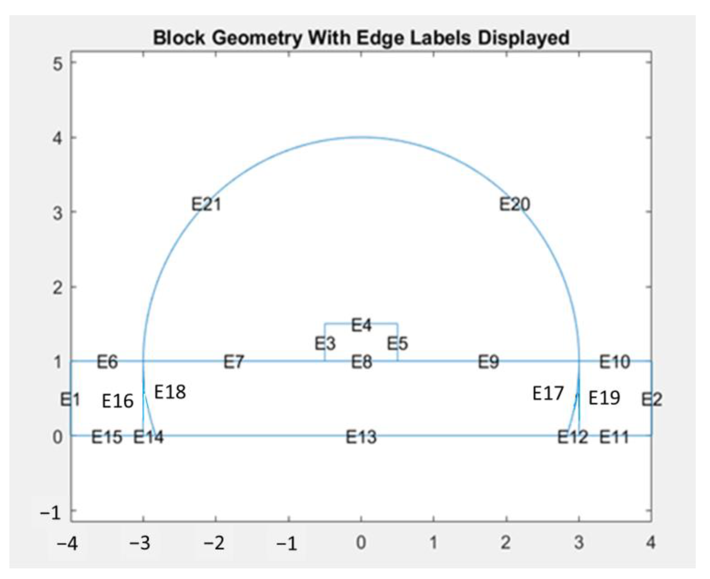
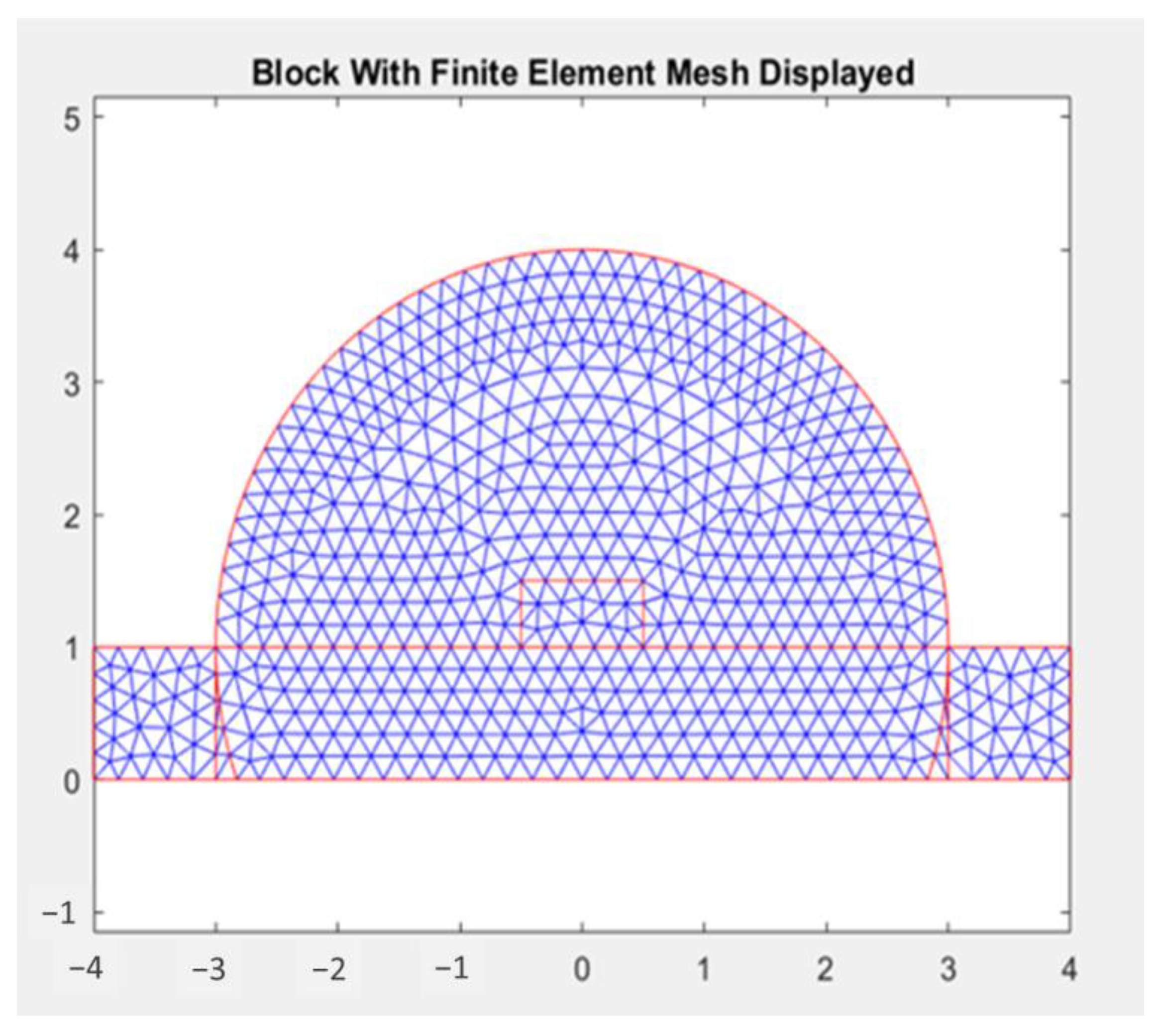
3.1. Simplify from 3D to 2D Thermal Modeling for Steady State

For the general case of a three-dimensional (3D) structure of a pc-WLED, the spatial temperature distribution in the 3D packaging volume can be defined by solving the heat diffusion equation [26]:
k 2 T + q ˙ = ρ   C p T t ,
where
2 = 2 x 2 + 2 y 2 + 2 z 2 .
2 is the Laplace operator, k is the thermal conductivity, q ˙ is the heat flux, ρ is the density, Cp is the specific heat, and T is the temperature, which is a function of a space and time.
At steady state T t = 0, the heat diffusion can be reduced as follows:
k 2 T + q ˙ = 0 .
Generally, a 3D thermal model is built to determine the temperature distribution inside the considered volume. The model can be transient or steady-state thermal in type. The main steps vary depending on the software; however, they can include selection of the type of thermal model, building the geometrical shape, and setting the values of the thermal parameters. Finally, verification with experiments, other simulations, or computation is performed to ensure the accuracy of the built model. It is difficult to build the geometrical structure given the multiple components or a complex structure and special shape. This can be time-consuming and reduce the simulation’s efficiency. Thus, it is necessary to develop a fast and accurate simulation for these cases.
The packaging structure of pcW-LEDs can be remote packaging, conformal coating, or a phosphor dome. As illustrated in Figure 4a, the 3D structure of a phosphor dome includes the substrate, blue LED die and phosphor dome, which is a mixture of silicone gel with yellow phosphor at a certain weight concentration. To simulate the temperature in a phosphor dome containing yellow phosphor, it is necessary to create a 3D model of the substrate, blue LED die, and phosphor dome; the thermal parameters are set correspondingly before running the simulation and analyzing the results.
It is interesting that when we analyze the characteristics of the structure of the phosphor dome, the packaging structure in the hemispherical package volume is highly symmetrical around the z-axis. As shown in Figure 4b–d, along the rotation direction in the z direction, we can see the similarity in shape at different cross sections. Based on this characteristic of the phosphor dome structure, a more convenient and simpler 2D model can be obtained from the 3D model. The temperature distribution in the cross-section planes around the z-axis is highly uniform. Since the volume of the blue LED die is lower than the encapsulant volume, the temperature distribution in other planes around the z-axis can be assumed to be the same as the temperature distribution in the plane (x–z). For example, the temperature distribution in the plane (x,z) is the same as that in the plane (y,z). If we know the temperature in the cross section in the plane (x,z), we can deduce the temperature distribution in the hemispherical package volume. This is an innovative way of simulating the temperature distribution in the region of the phosphor dome structure containing yellow phosphor material.
With the above argumentation and assumptions, the heat transfer equation in 3D space can be reduced to 2D space. We then find the temperature distribution in the 2D space of the plane (x–z). The heat transfer equation at the steady state for (x–z) is
k ( 2 T x 2 + 2 T z 2 ) +   q ˙ = 0 .
At the steady state, the heat flux is constant over time so that q ˙ = 0 . Thus, the remaining step for solving the problem of the 2D temperature distribution is defining the boundary conditions.

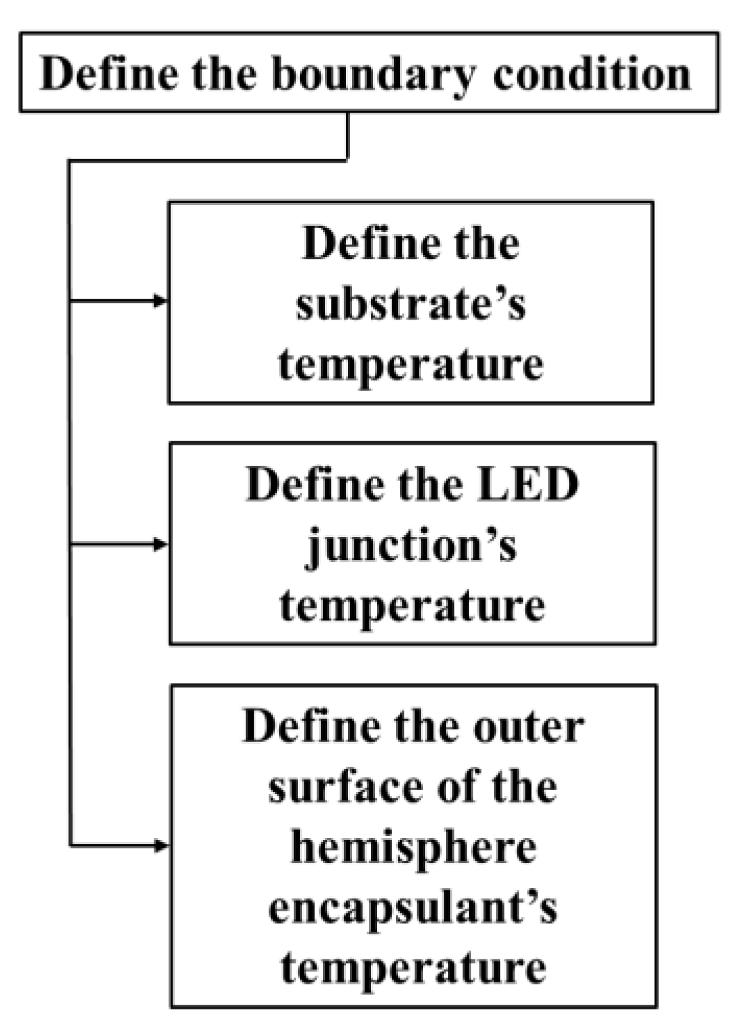
3.2. The Boundary Conditions

The boundary conditions for solving the problem of 2D space temperature distribution include the temperature of the substrate, the temperature of the LED die boundary, and the temperature of the outer surface of the hemispherical encapsulant. The process for boundary condition determination is shown in Figure 5.
The temperature of the substrate was defined using the thermal couple located at the bottom surface of the substrate. The thermal conductivity gel was used at the interface of the thermocouple and substrate. The working mode of the thermocouple was set with a time interval small enough that it could detect the temperature change from the initial state to the steady state in real time. Next, an electrical current for pc-LEDs was injected and the thermal couple was turned on. Finally, we obtained the temperature of the substrate at a steady state that corresponded to different injection electrical currents.
The temperature of the LED die boundary was assumed to be the same as the temperature of the junction region. The temperature of the junction region was calculated using the following equation [27,28]:
T j = T a + R t h · U · I · ( 1 η ) ,
where T j is the LED junction temperature, T a is the ambient temperature, R t h is the thermal resistance (K/W) or (°C/W), U is the forward voltage for LED (V), I is the injection electrical current for the pc-WLED (A), and η is the radiant optical efficiency of pc-WLEDs.
The temperature of the outer surface of the hemispherical encapsulant was defined by using a thermal camera to detect the temperature at a point on the surface of hemisphere after powering the pc-WLED and waiting for the temperature to reach the steady state. The temperature of the outer surface at different points on the surface of the hemispherical encapsulant was assumed to be uniform.

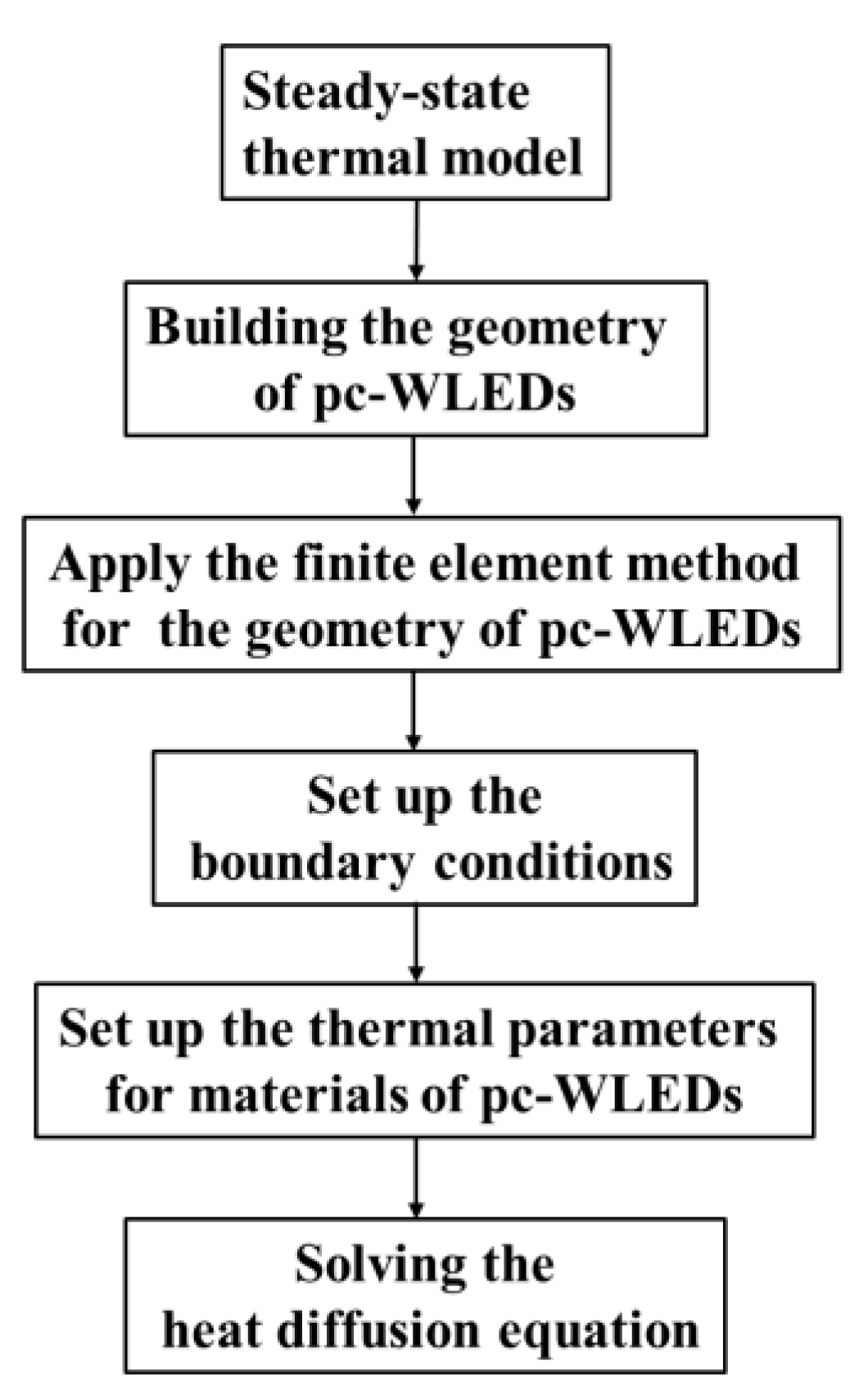
3.3. Simulation Flowchart

The simulation flowchart is shown in Figure 6. A thermal model for a steady-state pc-WLED was built by using MATLAB software (version R2017b) [29,30]. The main steps were as follows. Firstly, the type of model in MATLAB programming was defined as a steady-state thermal model. Secondly, the 2D structure of the pc-LED was programmed to have the same parameters as the side view of the real sample. The geometrical parameters are listed in Table 1. The third step was applying the finite element method to the 2D structure of the pc-LED. The block of the 2D structure of the pc-LED meshed with finite elements. The fourth step was setting up the boundary conditions of the block of the 2D structure of the pc-LED. The values of the temperature of the substrate, blue LED die boundary, and the outer surface of the hemispherical encapsulant were inserted. The temperature for the boundary condition in the simulation is shown in Table 2. For convenience, the temperature was set to 35 °C for the outer surface of the hemispherical encapsulant. The fifth step was to input the material parameters. The thermal parameters of the material included the substrate thermal conductivity, blue LED chip thermal conductivity, and silicone–phosphor matrix radius thermal conductivity. The thermal parameters of the material in the simulation are shown in Table 3. The final step was solving the heat diffusion equation. After running the program of the thermal model in MATLAB, the corresponding temperature distribution was obtained for further analysis.

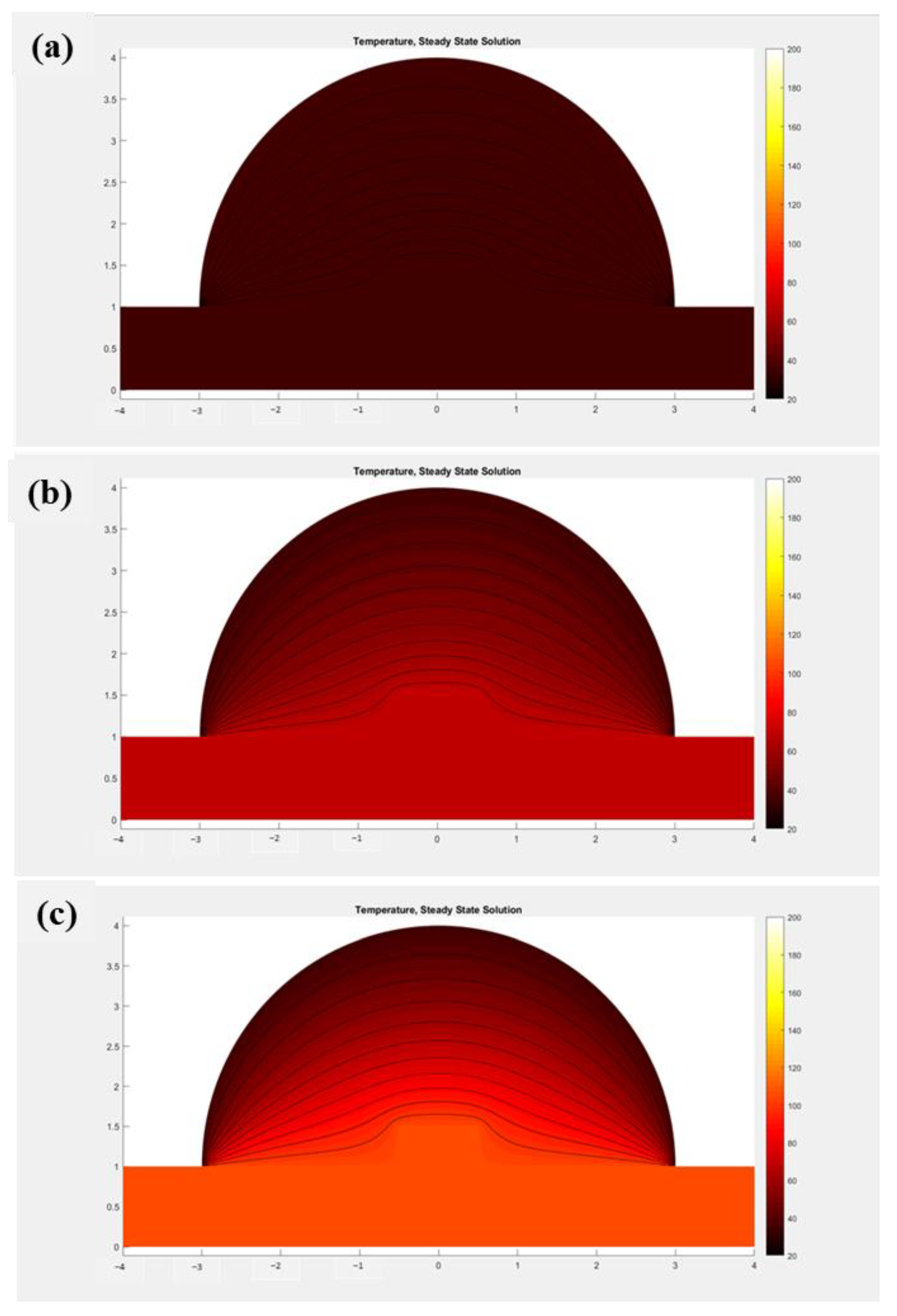
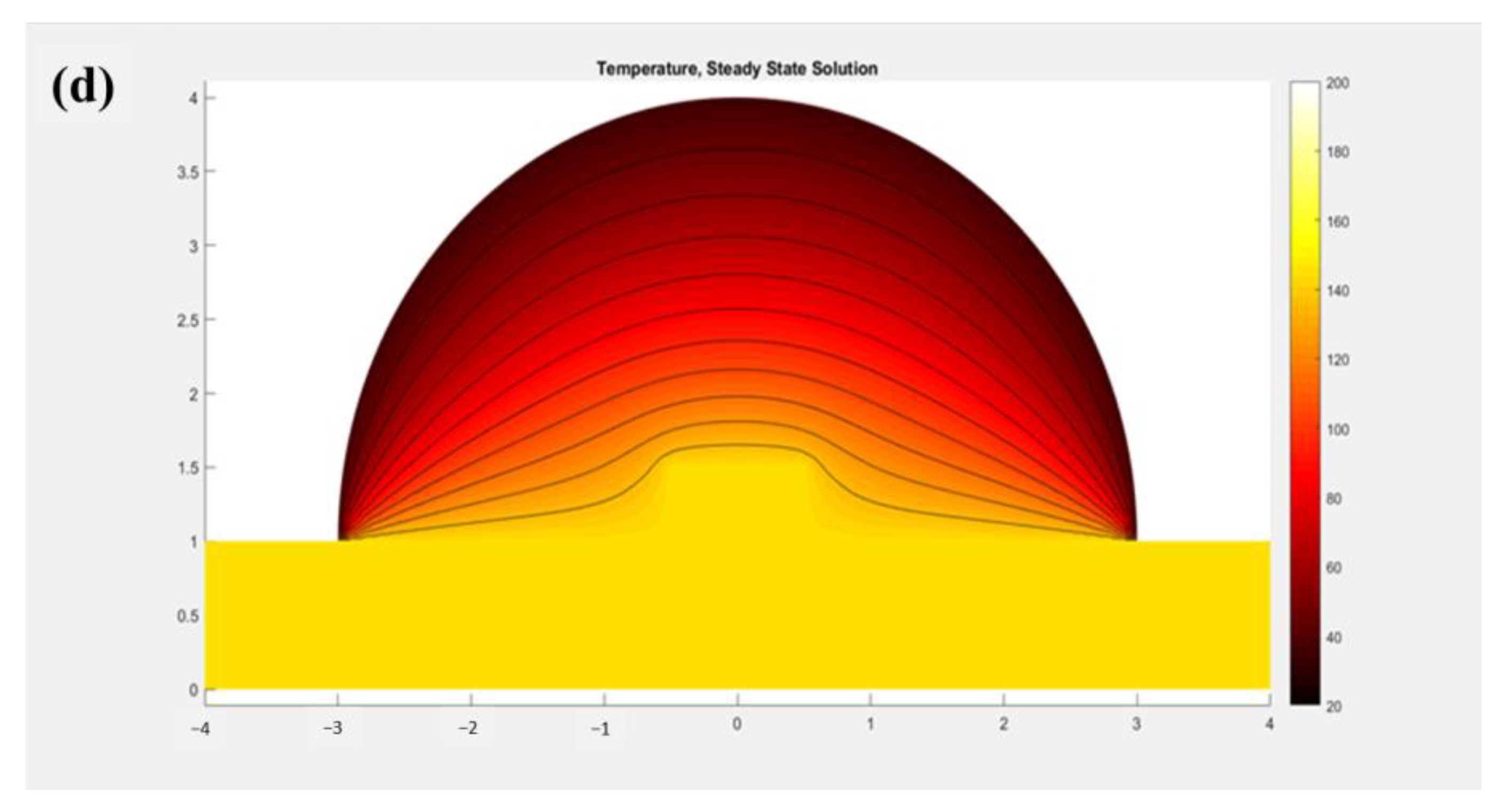
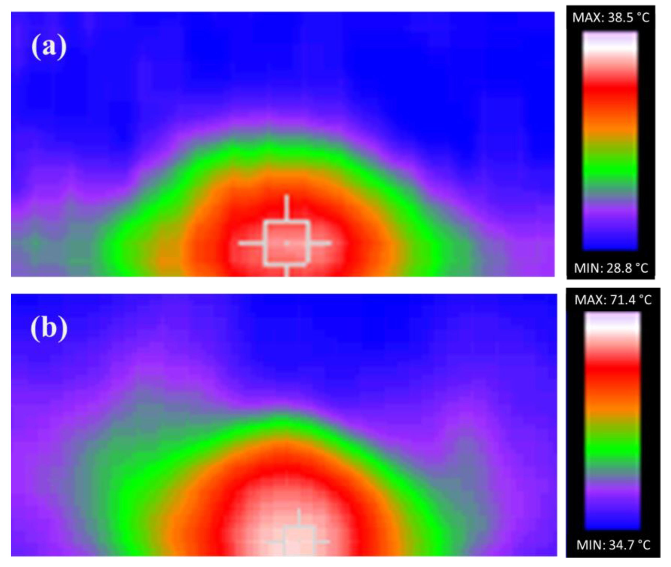
4. Simulation Results and Discussion

Figure 7 shows the 2D structure of the pc-WLED in the simulation. The block includes the three main regions of the substrate, a blue LED die, and a matrix of silicone–yellow phosphor. Each edge is labeled to help with setting boundary conditions. The block of the 2D structure of the pc-LED meshed with finite elements. The corresponding results are shown in Figure 8.
Figure 9 shows the results of the heat transfer equation at the steady state, corresponding to different injection currents. The injection currents used range from low to high, including 50 mA, 200 mA, 350 mA, and 500 mA. For each injection current, we used a set of corresponding boundary conditions.
The simulation results of applying the thermal model at a steady state for injection currents of 50 mA, 200 mA, and 350 mA are shown in Figure 9a–c, respectively. At a low injection current of 50 mA, the temperature distribution was more uniform than with 200 mA or 350 mA. Also, as higher injection currents were used, a higher temperature was seen in the total package region of the pc-WLED.
The simulation results of applying the thermal model at a steady state for a high injection current of 500 mA are shown in Figure 9d. The results show that when using a higher injection current, the temperature distribution showed a clear difference in the substrate region, in the region surrounding the LED die, and in the encapsulant region. In detail, the temperature decreased gradually from the LED die to the outer surface, which is the interface between the encapsulant and the ambient air. The temperature distribution showed that the farther the region was from the LED die, the lower the temperature. This distance-dependent temperature behavior is significant for packaging technology in that it indicates that one should locate the phosphor far from the blue LED die to avoid the temperature affecting the phosphor’s functions. It is also especially helpful for thermal management when operating the pc-WLED at a high injection current.
There was a large range in the temperature distribution. The temperature at the substrate and LED die was always higher than at the silicone–phosphor region. This difference is related to the thermal conductivity of each region. The thermal conductivity of the substrate was higher than that of the silicone–phosphor region. In other words, the thermal resistance of the silicone–phosphor region was higher than that of the substrate, so the heat from the blue LED region conducts toward the substrate region more easily than toward the silicone–phosphor region, where the thermal resistance is higher. Thus, we expect to see a higher temperature in the substrate region.
The results also indicated that it would improve the thermal conductivity of the mixture of silicone–phosphor if we conducted the heat from the LED die region to the outer surface air. Once the thermal conductivity is enhanced, it helps reduce the heat that accumulates in the packaging volume. Therefore, it reduces the effect of heat on the quality of the pc-WLED by, e.g., reducing thermal quenching and reducing the junction temperature, thus increasing the lifespan and ensuring the chromaticity is stable for output light.
A higher injection current causes the temperature of the LED and substrate region to become very high. Thus, it is important to operate pc-WLEDs at a moderate value or consider a suitable heat dissipation method to remove the heat from the LED and surrounding region.

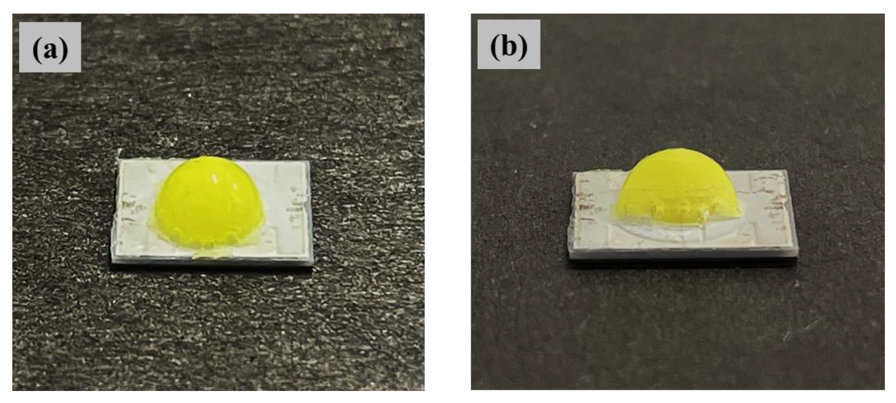
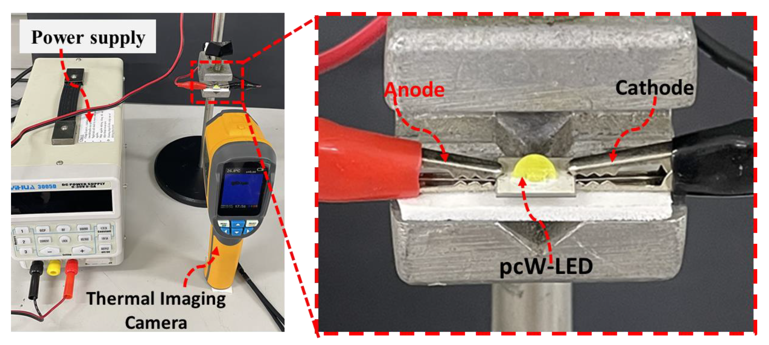
5. Experiments for the Determination of the Temperature Distribution of the Phosphor Region in the Hemispherical Packaging Structure

To confirm the similarity between the simulation results, we conducted an experiment. The utilized pcW-LED samples and the experimental setup for the determination of the temperature distribution using a thermal camera are shown in Figure 10 and Figure 11, respectively. Figure 10a shows the sample of the hemispherical packaged phosphor dome structure, which was prepared through a packaging processing using a submount substrate, blue LED die, gold alloy wire for electrode bonding, yellow phosphor (YAG: Ce), and silicone gel. According to the purpose of this experiment, a pc-WLED in the hemispherical packaged structure was prepared using the parameters in Table 1. The concentration of yellow phosphor used in the hemispherical packaged region was 7.5 wt %. The average correlated color temperature (CCT) of this pcW-LED was 5500 K when operated at an injection current of 50 mA. To the best of our knowledge, the temperature distribution within a pc-WLED has not been measured directly in any practical way yet. Furthermore, it is not easy to use a thermocouple to detect the temperature distribution inside a packaged volume that contains yellow phosphor (YAG: Ce) and silicone gel. In this case, if a thermal camera is used to record the temperature, we can obtain spatial thermal imaging of the temperature distribution of a hot surface emitting infrared radiation. It is important to note that, when using a thermal camera to record the temperature, the recorded result is only the temperature distribution of the outer side of the packaged volume rather than the temperature inside the packaged volume of the pcW-LED. To overcome this difficulty, the sample of the hemispherical packaged phosphor dome structure was cut in half to show a cross section, as shown in Figure 10b. Next, the temperature distribution in this cross section of the pcW-LED was detected by a thermal imaging camera. Then, the temperature distribution in the packed structure was deduced from that of the cross section.
Figure 11 shows the experimental setup for determining the temperature distribution of the cross section of a sample of the phosphor dome packaged structure. The sample pcW-LEDsA was operated in a constant-current mode and supplied from the power supply. The temperature was recorded by a thermal imaging camera placed opposite the pcW-LED sample. After the pcW-LED sample was powered, a state of thermal equivalence was reached after 15 min. Then, the temperature of the cross section of the sample pcW-LED was recorded by a thermal imaging camera (HT-02, Hti Thermal Imaging Camera, Dongguan Xintai Instrument Co., Ltd., Dongguan City, China), which has a spatial resolution of 3600 pixels. The emissivity was set to 0.90, according to the recommendations in the manual for the plastic material.
The sample was operated at low injection electrical currents of 50 mA and 200 mA to avoid thermal damage to the sample pcW-LED. Then, the temperature distribution at the cross section of the sample pcW-LED at each corresponding injection current was detected. The corresponding results are shown in Figure 12. As shown in Figure 12a,b, the ranges of the minimum and maximum temperatures for the two levels of injection currents of 50 mA and 200 mA were 28.8–38.5 °C, and 34.7–71.4 °C, respectively. The temperatures of the hotspot of the injection current with 50 mA and 200 mA were 38.5 °C and 71.1 °C, respectively. These results show that when using a higher injection current, the temperature of the hotspot is higher. On the other hand, the difference in color in the detected temperature distribution indicates a clear difference in the LED die surrounding region, and the encapsulant region. In detail, the temperature decreased gradually from the LED die region to the outer surface, which is the interface between the encapsulant and the ambient air. These temperature distribution results show an inversely proportional relationship between the temperature value and the distance to the region containing the blue LED die. However, it can be seen that the behavior of temperature at the cross section shows a close match between the simulation and the experimental results.

6. Conclusions

The packaging structure of pc-WLEDs in which the matrix of silicone–yellow phosphor is shaped as a hemisphere was studied in terms of the temperature characteristics corresponding to different injection currents. Based on the finite element method and using MATLAB software (version R2017b), a numerical thermal model was constructed to estimate the temperature distribution in the hemispherical packaging volume of white LED at a steady state.
To create the model, we began by simplifying from 3D space to 2D space, building the 2D structure of the pc-WLED, defining the boundary conditions at steady state, and setting the thermal parameters for the materials. Finally, we solved a heat diffusion equation to find the spatial temperature distribution in the packaging volume.
This model was applied for the simulation of the temperature distribution of hemispherical pc-WLEDs; we injected different injection currents, including 50 mA, 200 mA, 350 mA, and 500 mA.
The simulation results clearly show the influence of the injection current and thermal conductivity difference on the temperature in different regions of the packaged part. The higher the injection current, the higher the temperature of the pc-WLED. The hottest region was the region close to the LED die, while the temperature gradually decreased from the LED die to the outer surface. These results indicate that phosphor should be located far from the LED die to avoid the heat having an effect on the phosphor’s efficiency.
The temperature distribution when using 500 mA showed that the hottest regions are located at the LED die and substrate. Thus, we need to carefully consider heat dissipation solutions when using a high operating power mode. The results also indicate that the injection current should be as moderate as possible to avoid possible overheating.
The sample of the hemispherical packaged structure was prepared and cut in half to show the cross-sectional surface. A thermal imaging camera was utilized to detect the temperature distribution in the cross section of the sample pcW-LEDs. The similarity between the experimental and simulation results was confirmed. The detected temperature distribution showed an inversely proportional relationship between the temperature and the distance from the region containing the blue LED die.
Methods to improve the thermal conductivity of the encapsulant region should be studied further to reduce the accumulated heat in the LED die region. This improvement will be meaningful for high-power pc-WLEDs packaging technology in terms of thermal management efficiency.

Author Contributions

Conceptualization, Q.-K.N.; Data curation, Q.-K.N.; Formal analysis, T.-H.-T.V.; Methodology, Q.-K.N.; Writing—original draft, Q.-K.N.; Writing—review and editing, T.-H.-T.V. All authors have read and agreed to the published version of the manuscript.

Funding

This research is funded by University of Science, VNU-HCM under grant number T2023-11.

Data Availability Statement

The data presented in this study are available on request from the corresponding author.

Acknowledgments

The authors would like to thank their sponsors from the VNUHCM-University of Science, Ho Chi Minh City, Vietnam. This research is funded by University of Science, VNU-HCM under grant number T2023-11.

Conflicts of Interest

The authors declare no conflict of interest.

References

  1. Schubert, E.-F.; Kim, J.-K. Solid-state light sources getting smart. Science 2005, 308, 1274–1278. [Google Scholar] [CrossRef] [PubMed]
  2. Narendran, N.; Gu, Y. Life of LED-Based White Light Sources. J. Disp. Technol. 2005, 1, 167–171. [Google Scholar] [CrossRef]
  3. Schubert, E. Light-Emitting Diodes, 2nd ed.; Cambridge University Press: Cambridge, UK, 2006. [Google Scholar] [CrossRef]
  4. Chang, M.-H.; Das, D.; Varde, P.; Pecht, M. Light emitting diodes reliability review. Microelectron. Reliab. 2012, 52, 762–782. [Google Scholar] [CrossRef]
  5. Efremov, A.-A.; Bochkareva, N.-I.; Gorbunov, R.-I.; Lavrinovich, D.-A.; Rebane, Y.-T.; Tarkhin, D.-V.; Shreter, Y.-G. Effect of the joule heating on the quantum efficiency and choice of thermal conditions for high-power blue InGaN/GaN LEDs. Semiconductors 2006, 40, 605–610. [Google Scholar] [CrossRef]
  6. Lin, Y.-C.; Bettinelli, M.; Sharma, S.-K.; Redlich, B.; Speghini, A.; Karlsson, M. Unraveling the impact of different thermal quenching routes on the luminescence efficiency of the Y3Al5O12:Ce3+ phosphor for white light emitting diodes. J. Mater. Chem. C 2020, 8, 14015. [Google Scholar] [CrossRef]
  7. Narendran, N.; Gu, Y.; Jayasinghe, L.; Freyssinier, J.-P.; Zhu, Y. Long-term performance of white LEDs and systems. In Proceedings of the First International Conference on White LEDs and Solid-State lighting, Tokyo, Japan, 26–30 November 2007; pp. 174–179. [Google Scholar]
  8. Singh, P.; Tan, C.-M. Degradation Physics of High-Power LEDs in Outdoor Environment and the Role of Phosphor in the degradation process. Sci. Rep. 2016, 6, 24052. [Google Scholar] [CrossRef] [Green Version]
  9. Davis, J.L.; Mills, K.-C.; Bobashev, G.; Rountree, K.-J.; Lamvik, M.; Yaga, R.; Johnson, C. Understanding chromaticity shifts in LED devices through analytical models. Microelectron. Reliab. 2018, 84, 149–156. [Google Scholar] [CrossRef]
  10. Yazdan Mehr, M.; Bahrami, A.; Van Driel, W.-D.; Fan, X.-J.; Davis, J.-L.; Zhang, G.-Q. Degradation of optical materials in solid-state lighting systems. Int. Mater. Rev. 2020, 65, 102–128. [Google Scholar] [CrossRef] [Green Version]
  11. Su, Y.-F.; Yang, S.-Y.; Hung, T.-Y.; Lee, C.-C.; Chiang, K.-N. Light degradation test and design of thermal performance for high-power light-emitting diodes. Microelectron. Reliab. 2012, 52, 794–803. [Google Scholar] [CrossRef]
  12. Baran, K.; Leśko, M.; Wachta, H.; Różowicz, A. Thermal Modeling and Simulation of High Power LED Module. AIP Conf. Proc. 2019, 2078, 020048. [Google Scholar] [CrossRef]
  13. Fu, H.K.; Wang, C.P.; Chiang, H.C.; Chen, T.T.; Chen, C.L.; Chou, P.T. Evaluation of temperature distribution of LED module. Microelectron. Reliab. 2013, 53, 554–559. [Google Scholar] [CrossRef]
  14. Chen, M.; Xu, C.; Xu, K.; Zheng, L. Thermal simulation and analysis of flat surface flip-chip high power light-emitting diodes. J. Semicond. 2013, 34, 124005. [Google Scholar] [CrossRef]
  15. Smet, P.F.; Parmentier, A.B.; Poelman, D. Selecting Conversion Phosphors for White Light-Emitting Diodes. J. Electrochem. Soc. 2011, 158, R37. [Google Scholar] [CrossRef] [Green Version]
  16. Ying, S.-P.; Fu, H.-K.; Tang, W.-F.; Hong, R.-C. The Study of Thermal Resistance Deviation of High-Power LEDs. IEEE Trans. Electron Devices 2014, 61, 2843–2848. [Google Scholar] [CrossRef]
  17. Górecki, K.; Ptak, P. Compact Modelling of Electrical, Optical and Thermal Properties of Multi-Colour Power LEDs Operating on a Common PCB. Energies 2021, 14, 1286. [Google Scholar] [CrossRef]
  18. Liu, Z.; Liu, S.; Wang, K.; Luo, X. Optical Analysis of Phosphor’s Location for High-Power Light-Emitting Diodes. IEEE Trans. Device Mater. Reliab. 2009, 9, pp. 65–73. [Google Scholar] [CrossRef]
  19. Chen, K.J.; Lin, B.C.; Chen, H.C.; Shih, M.H.; Wang, C.H.; Kuo, H.T.; Tsai, H.H.; Kuo, M.Y.; Chien, S.H.; Lee, P.T. Effect of the Thermal Characteristics of Phosphor for the Conformal and Remote Structures in White Light-Emitting Diodes. IEEE Photonics J. 2013, 5, 8200508. [Google Scholar] [CrossRef]
  20. Tan, C.M.; Singh, P.; Zhao, W.; Kuo, H.C. Physical Limitations of Phosphor layer thickness and concentration for White LEDs. Sci. Rep. 2018, 8, 2452. [Google Scholar] [CrossRef] [Green Version]
  21. Nemitz, W.; Fulmek, P.; Nicolics, J.; Reil, F.; Wenzl, F.P. On the determination of the temperature distribution within the color conversion elements of phosphor converted LEDs. Sci. Rep. 2017, 7, 9964. [Google Scholar] [CrossRef] [Green Version]
  22. Zhang, Y.Z.; Li, C.X.; Wang, Y.; Ran, L.L. Thermal simulation and analysis of high-power white LED light. In Advances in Materials Science, Energy Technology and Environmental Engineering; Patty, A., Zhou, P., Eds.; Taylor & Francis Group: London, UK, 2017; ISBN 978-1-138-19668-1. [Google Scholar]
  23. Chatterjee, A.; Senawiratne, J.; Li, Y.; Detchprohm, T.; Zhu, M.; Xia, Y.; Zhao, W.; Plawsky, J.L.; Wetzel, C. Junction Temperature Simulation of Gallium Nitride Green Light Emitting Diodes Using COMSOL. In Proceedings of the COMSOL Conference, Boston, MA, USA, 24 October 2007. [Google Scholar]
  24. Kim, J.P.; Jeon, S. Investigation of Light Extraction by Refractive Index of an Encapsulant, a Package Structure, and Phosphor. IEEE Trans. Compon. Packag. Manuf. Technol. 2016, 6, 1815–1819. [Google Scholar] [CrossRef]
  25. Ma, M.; Mont, F.W.; Yan, X.; Cho, J.; Schubert, E.F.; Kim, G.B.; Sone, C. Effects of the refractive index of the encapsulant on the light-extraction efficiency of light-emitting diodes. Opt. Express 2011, 19, A1135–A1140. [Google Scholar] [CrossRef] [PubMed] [Green Version]
  26. Incropera, F.P.; DeWitt, D.P.; Bergman, T.L.; Lavine, A.S. Fundamentals of Heat and Mass Transfer, 5th ed.; J. Wiley: New York, NY, USA, 2002. [Google Scholar]
  27. Stefanie, R.; Rainer, H. The Thermal Measurement Point of LEDs; Application Note No. AN085; OSRAM Opto Semiconductors: Munich, Germany, 2021. [Google Scholar]
  28. Ying, S.; Fu, H.; Hong, R. The Study of Thermal Resistance Measurement of Multichip LED. IEEE Trans. Electron Devices 2015, 62, 3291–3295. [Google Scholar] [CrossRef]
  29. The MathWorks, Inc. Partial Differential Equation Toolbox for Use with MATLAB; The MathWorks, Inc.: Natick, MA, USA, 1995. [Google Scholar]
  30. Heat Transfer. Mathwork.com. Available online: https://www.mathworks.com/help/pde/heat-transfer-and-diffusion-equations.htmls_tid=CRUX_lftnav (accessed on 19 April 2022).
Figure 1. Geometry of white light pc-LED using a hemispherical structure.
Jcs 07 00301 g001
Figure 2. Difference in excitation and converted wavelengths.
Jcs 07 00301 g002
Figure 3. Mechanism of heat generation inside the blue LED die.
Jcs 07 00301 g003
Figure 4. Graphical illustration of the simplified process (3D to 2D) of building the thermal modeling process: (a) 3D view of pcW-LED phosphor dome packaged structure; (b) cross section at plane (x–z) and (y–z); (c,d) indicate the similarity between the cross sections at plane (x–z) and (y–z).
Jcs 07 00301 g004
Figure 5. The process of boundary condition determination.
Jcs 07 00301 g005
Figure 6. The main steps of the simulation.
Jcs 07 00301 g006
Figure 7. The 2D structure of the pc-WLED.
Jcs 07 00301 g007
Figure 8. Finite element method meshed for 2D geometry of the pc-WLED.
Jcs 07 00301 g008
Figure 9. Temperature distributions at steady state corresponding to different injection electrical currents: (a) 50 mA, (b) 200 mA, (c) 350 mA, and (d) 500 mA.
Jcs 07 00301 g009aJcs 07 00301 g009b
Figure 10. (a) Sample of phosphor dome packaged structure, and (b) sample of phosphor dome packaged structure cut in half.
Jcs 07 00301 g010
Figure 11. Experimental setup for determination of the temperature distribution of a sample of phosphor dome packaged structure cut in half (left), and enlarged area (right).
Jcs 07 00301 g011
Figure 12. Temperature distribution at steady state corresponding to different injection electrical currents: (a) 50 mA and (b) 200 mA.
Jcs 07 00301 g012
Table 1. Geometrical parameters used in the simulation.
NameValueUnit
Substrate thickness1mm
Blue LED die thickness0.5mm
Blue LED die width0.7mm
Silicone–phosphor matrix radius3.0mm
Table 2. The temperature inputs for the boundary conditions in the simulation.
Driven Current
(mA)
Temperature of pc-WLED Substrate
(°C)
Temperature of LED Die
(°C)
503637
2006971
350103108
500142149
Table 3. Thermal parameters of the material in the simulation.
NameValueUnit
Substrate thermal conductivity400W/(m·K)
Blue LED die thermal conductivity130W/(m·K)
Silicone–phosphor matrix thermal conductivity0.2W/(m·K)
Disclaimer/Publisher’s Note: The statements, opinions and data contained in all publications are solely those of the individual author(s) and contributor(s) and not of MDPI and/or the editor(s). MDPI and/or the editor(s) disclaim responsibility for any injury to people or property resulting from any ideas, methods, instructions or products referred to in the content.

