Article

A Silicon-Photo-Multiplier-Based Camera for the Terzina Telescope on Board the Neutrinos and Seismic Electromagnetic Signals Space Mission

by
Leonid Burmistrov
on behalf of the NUSES Collaboration
Département de Physique Nuclèaire et Corpusculaire, Université de Genève, 1205 Genève, Switzerland
Current address: Ecole de Physique, Quai Ernest-Ansermet 24, 1205 Genève, Switzerland.
Instruments 2024, 8(1), 13; https://doi.org/10.3390/instruments8010013
Submission received: 26 October 2023 / Revised: 18 January 2024 / Accepted: 31 January 2024 / Published: 20 February 2024

Abstract

:
NUSES is a pathfinder satellite project hosting two detectors: Ziré and Terzina. Ziré focuses on the study of protons and electrons below 250 MeV and MeV gamma rays. Terzina is dedicated to the detection of Cherenkov light produced by ultra-high-energy cosmic rays above 100 PeV and ultra-high-energy Earth-skimming neutrinos in the atmosphere, ensuring a large exposure. This work mainly concerns the description of the Cherenkov camera, composed of SiPMs, for the Terzina telescope. To increase the data-taking period, the NUSES orbit will be Sun-synchronous (with a height of about 550 km), thus allowing Terzina to always point toward the dark side of the Earth’s limb. The Sun-synchronous orbit requires small distances to the poles, and as a consequence, we expect an elevated dose to be received by the SiPMs. Background rates due to the dose accumulated by the SiPM would become a dominant contribution during the last two years of the NUSES mission. In this paper, we illustrate the measured effect of irradiance on SiPM photosensors with a variable-intensity beam of 50 MeV protons up to a 30 Gy total integrated dose. We also show the results of an initial study conducted without considering the contribution of solar wind protons and with an initial geometry with Geant4. The considered geometry included an entrance lens as one of the options in the initial design of the telescope. We characterize the SiPM output signal shape with different μ-cell sizes. We describe the developed parametric SiPM simulation, which is a part of the full Terzina simulation chain.

1. Introduction

The NUSES (Neutrinos and Seismic Electromagnetic Signals) space mission aims to explore new technological and scientific pathways in cosmic-ray and multi-messenger astrophysics [1,2,3]. The NUSES satellite will have a ballistic trajectory without orbital control. At the beginning of life (BoL), it will operate at an altitude of 535 km. The high inclination of the 97.8 deg (LTAN = 18:00) orbit will allow a Sun-synchronous location of the satellite along the day–night boundary. The NUSES satellite will host two scientific apparatuses, namely, Zirè [4,5] and Terzina [2,6], and will operate for at least three years.
Zirè consists of a scintillating fiber tracker, a stack of plastic scintillator counters, an array of LYSO crystals, an active VETO system, and a Low-Energy Module (LEM). It will perform spectral measurements of electrons, protons, and light nuclei below a few to hundreds of MeV. Zirè will also test innovative detection techniques for 0.1–10 MeV photons and monitor the Van Allen radiation belt.
Terzina is a telescope specifically designed for the detection of the Cherenkov light emitted by extensive air showers (EASs) induced by ultra-high-energy cosmic rays (UHECRs) and neutrinos in the Earth’s atmosphere. We expect to detect proton-induced air showers with energies above 100 PeV for the first time from space. This constitutes a very relevant exploration for space-based instruments like POEMMA [7,8].
We briefly describe the telescope below, but this contribution is mainly devoted to the SiPM characterization, radiation tests, and simulations.

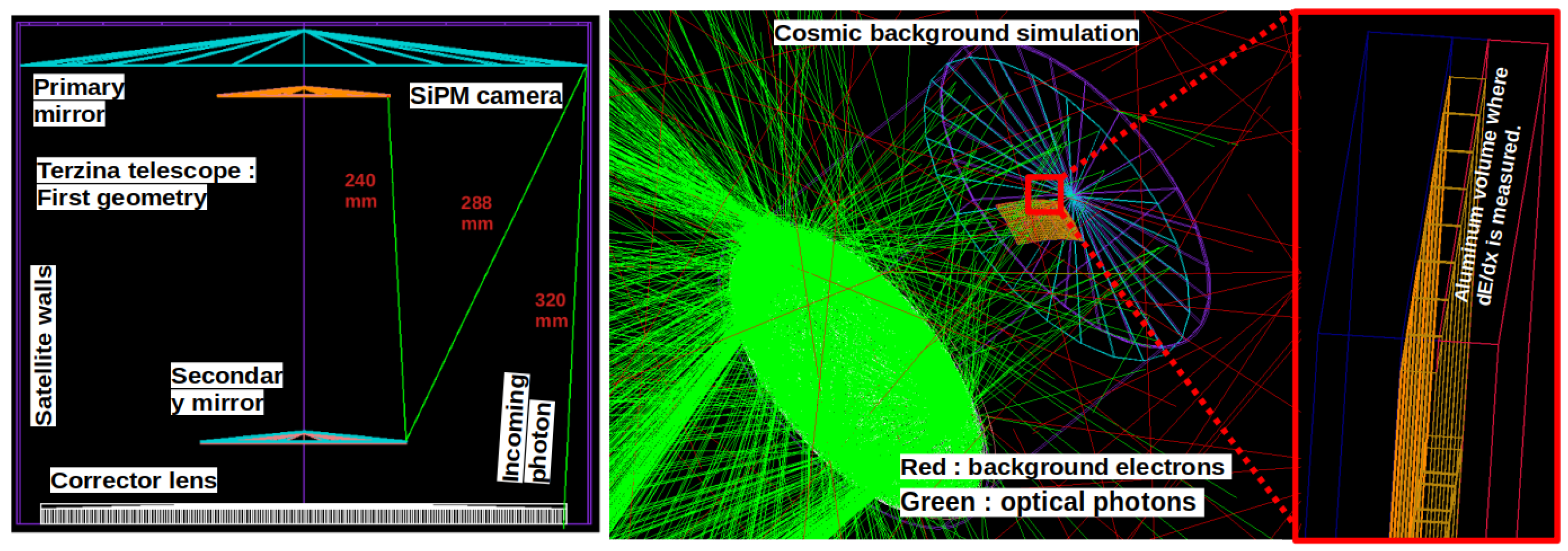
2. Terzina Telescope

Terzina is composed of an optical head unit; a focal plane assembly (FPA), including the photosensitive SiPM camera and the readout integrated circuits; a thermal control system; and an external harness and electronic unit, which is in a separate box, shielded from irradiation. The optical head unit is a Schmidt–Cassegrain near-UV–optical telescope.
The Terzina optical system achieves an effective area of about 0.1 m2 and an equivalent focal length of 930 mm, with the diameter of the circle containing 80% of the photons being less than 1 mm2. The results in this proceeding refer to the initial configuration. It consists of two hyperbolic mirrors (primary and secondary) and a corrector lens, integrated with the flat FPA in a hole at the center of the primary mirror. The corrective lens at the entrance of the telescope shields the internals from radiation; however, it is heavy, and we have considered moving it to the secondary mirror.
The Terzina photosensitive (detection) plane is composed of two rows of five SiPM arrays manufactured by FBK [9,10,11]. Each tile is made of 8 × 8 channels of 3 × 3 mm2 pixels. The sensitive areas of a pixel are limited by the packaging to about 2.4 × 2.7 mm2. We chose the NUV-HD-MT [10] (Near-Ultraviolet High-Density Metal Trench) technology provided by FBK for our application.

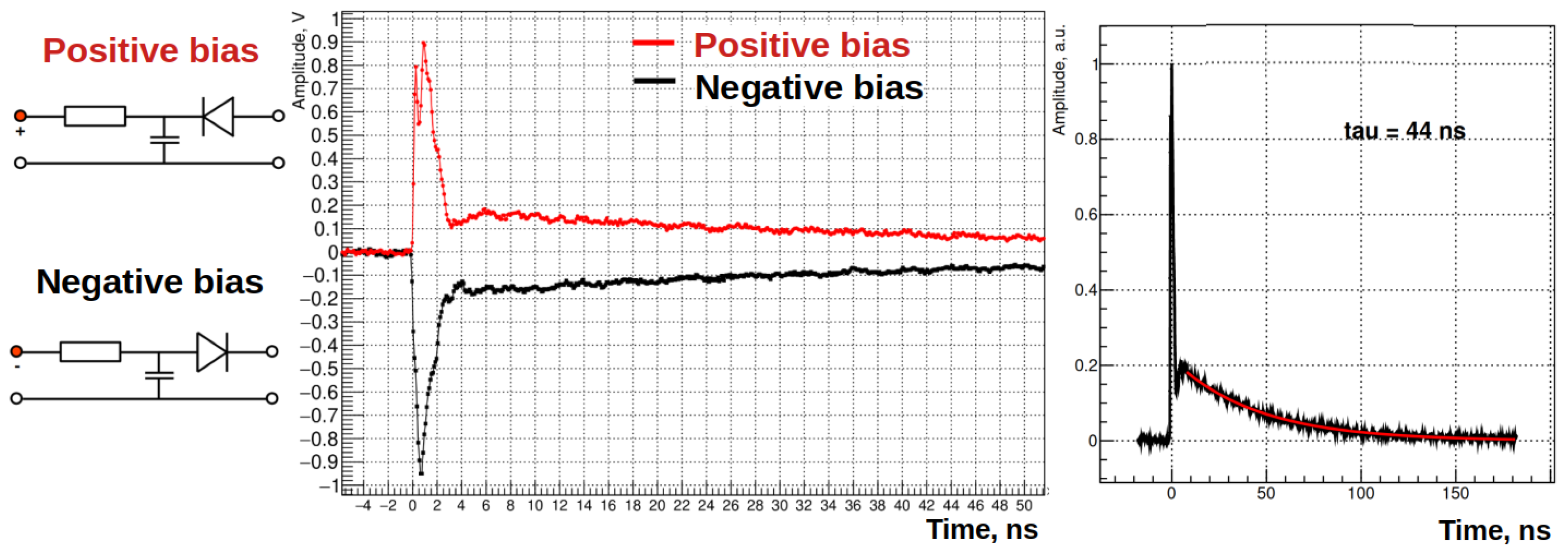
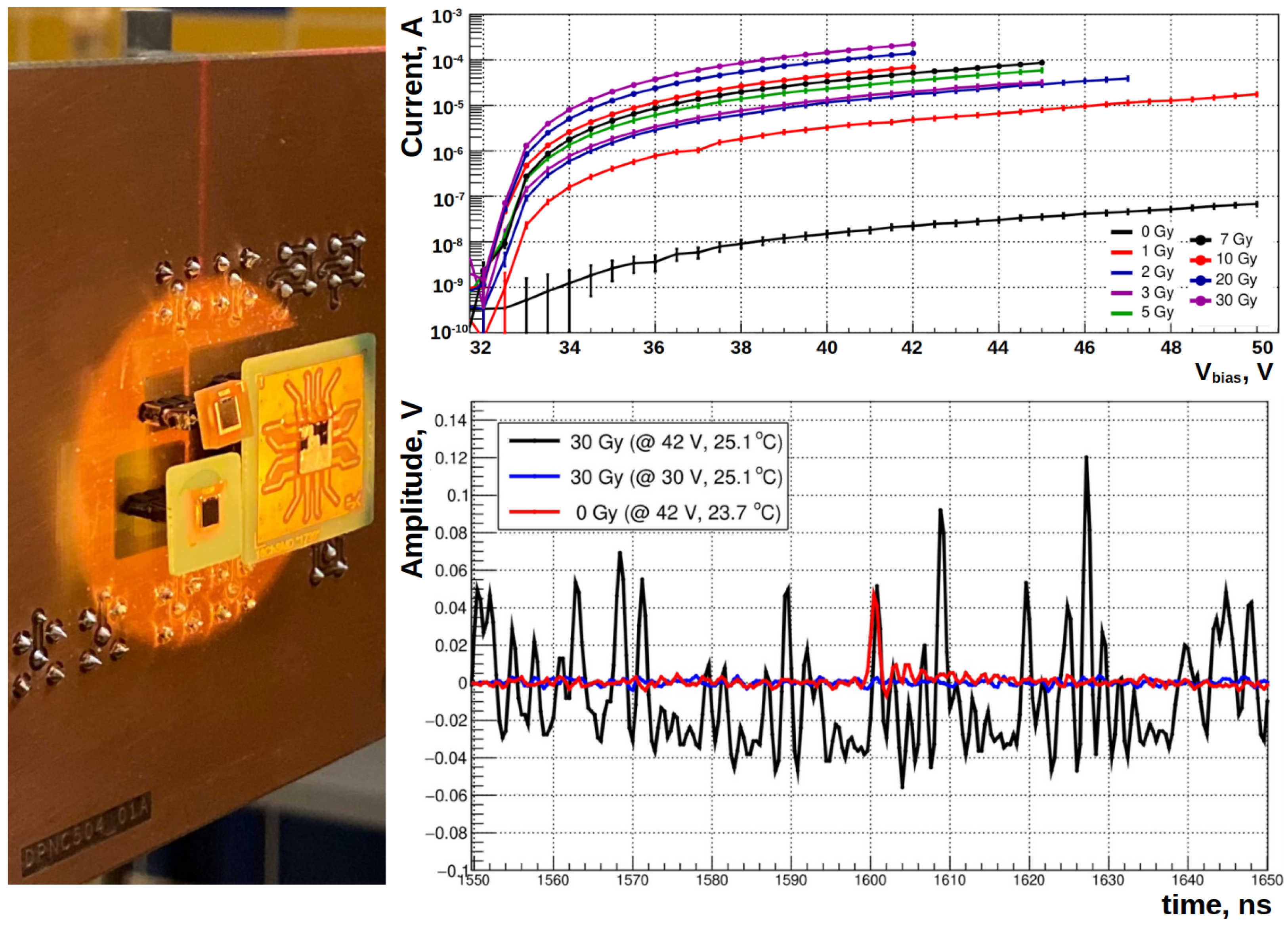
3. SiPM Signal Waveform Characterization

The design of the electronic readout chain and the SiPM simulation (Section 4) are dependent on the SiPM response and signal shape. As a result, we carried out SiPM characterization, which is covered in this part, along with a signal shape analysis.
Figure 1 (left panel) shows the bias and readout schematics of SiPMs. A SiPM operates at reverse bias voltage; however, it can be powered with positive and negative voltages, providing positive or negative output signals accordingly. This change of sign needs to be taken into account while designing and optimizing front-end electronics and the entire readout chain. In the case of single-photon operation or weak light fluxes, we are not able to see a signal with a conventional oscilloscope without an amplifier. Hence, we used a short-duration (∼25 ps) light-pulse laser with a 370 nm wavelength to flash all the μ-cells at the same time. As a result, we obtained a ∼1 V signal with a shape roughly equal to a single μ-cell response. We measured a fast signal rising edge of ∼200 ps with a 2 GHz bandwidth oscilloscope.
A SiPM signal tail can be fitted with an exponent, as shown in Figure 1 (right panel), and its duration can be quantified as an exponent decay time (τ). This time is a function of the μ-cell capacitance, hence its size. We did not observe any significant change in the signal shape with the variation in the bias voltage.
We performed a set of measurements with three different configurations: with LED (450 nm) and an integration sphere, with a laser (370 nm) and an integration sphere, and with a laser only. Figure 2 (left panel) summarizes the obtained results. As expected, the shortest decay time was measured with the laser. As the integration sphere induces an additional time spread, it has been removed.
If we want to minimize the pulse duration only, we have to choose a SiPM with a small μ-cell size. However, SiPMs with small μ-cells have a lower PDE due to a smaller fill factor, and the signal is linearly dependent on the PDE. Hence, the final choice of the SiPM μ-cell of 30 µm is considered to be a balance between these parameters.

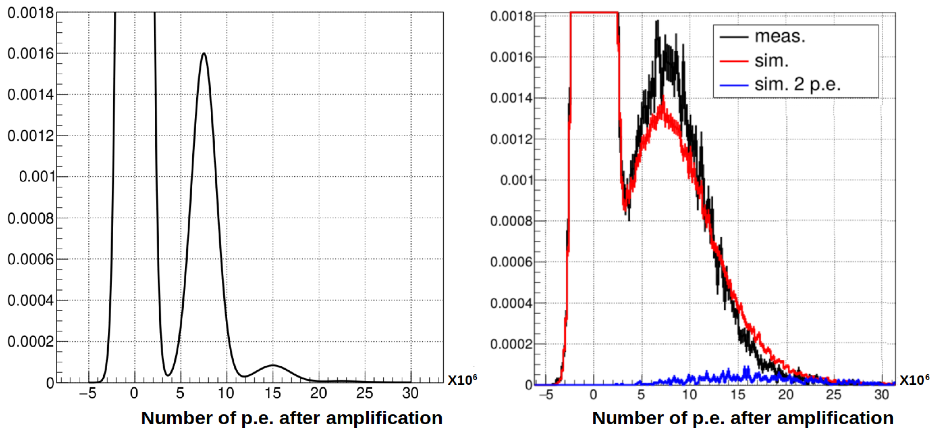
4. Parametric Simulation of the SiPM Response

The Terzina full simulation chain is a sophisticated instrument for assessing the experiment’s physics performance. Considering that the SiPM response affects the performance, we have developed lightweight simulation software that can be easily integrated into our framework.
In this section, we briefly discuss the SiPM response simulation, while an exhaustive description of the SiPM physics can be found in reference [11]. Our parametric simulation [12] takes the following as an input:
  • The pulse template of the SiPM response to a single p.e., where the amplitude is scaled linearly to increase the over-voltage;
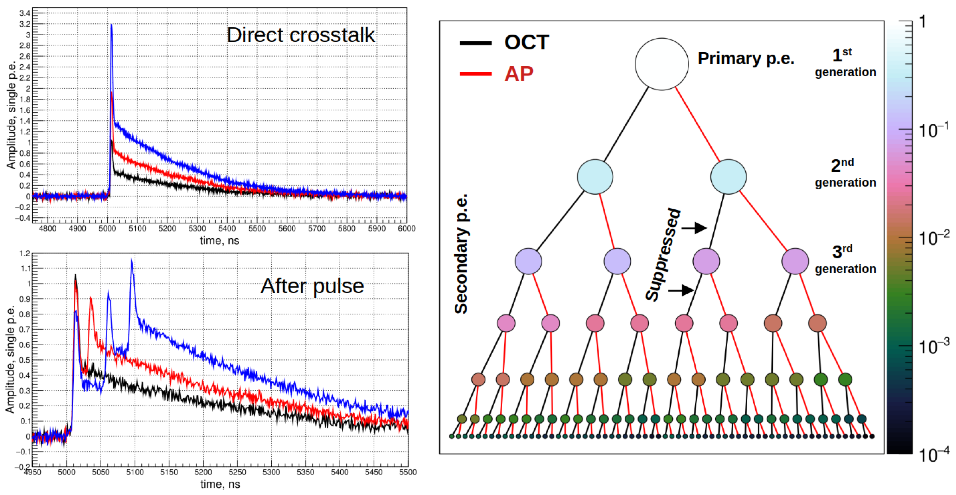
  • The probability of direct optical cross-talk (OCT) and after-pulse (AP) as a function of the SiPM over-voltage;
  • After-pulse decay time;
  • The root mean square error (RMSE) of the SiPM gain variation and the RMSE of the electronic noise.
The simulation is realized as a recursion of the physics processes: every time we generate the primary p.e., there is a probability of generating a secondary p.e. via OCT or AP (see Figure 3, left-top and left-bottom panels, respectively). The after-pulse process simulation takes into account a μ-cell recovery time, which strongly depends on the μ-cell area (and so too its capacitance mainly). The model does not take into account the over-voltage variations. The AP and OCT probabilities are functions of their mother avalanche amplitudes. We assume a linear dependency between the AP/OCT probability and the amplitude of the avalanche. (The initial probability of the AP/OCT is given for fully recovered μ-cell.)
The process history avalanche tree of a single p.e. generation is shown in the right panel of Figure 3. The AP and OCT probabilities depend on the history depth and the origin of the second p.e. generation. This is explained by the AP and OCT probability adjustment, which is a function of its mother avalanche amplitude: when a μ-cell is not fully recharged, it cannot generate a full avalanche, and so the probability of AP/OCT drops. To illustrate the net effect of the μ-cell recovery, we use the avalanche tree diagram. We set equal probabilities of AP and OCT to 30% and the decay time constant of the μ-cell recovery time to 50 ns. Starting from the third generation, one can see the slight suppression from the right (AF—red line) with respect to the left side (OCT—black line).
This simulation is a part of the full simulation chain of the Terzina telescope. It is used to estimate the trigger rates for the pure expected noise as a function of the electronic threshold. Our background is mostly sourced from the SiPM dark count rate (DCR) and the night-glow background (NGB).
Using this parametric simulation, we investigated two variables and their effects on the trigger rate for an identical electronic threshold:
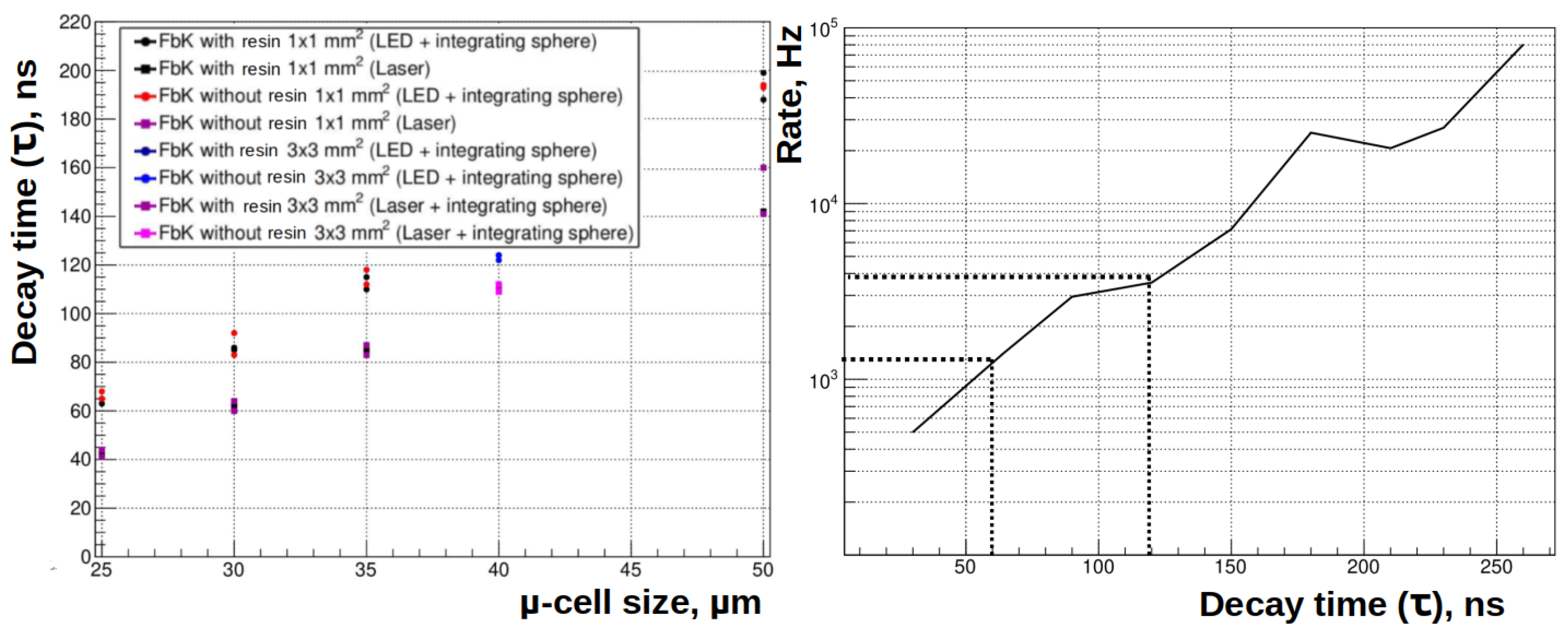
  • Signal decay time: see Figure 2 (right panel). We confirmed our expectation: in the case of the AC/DC coupling readout, by reducing the decay time of the SiPM signal, one can significantly reduce the fake rate while keeping the same sensitivity to the signal.
  • Different bandwidths of the electronics. We found a significant rate variation with the preamplifier bandwidth. However, the front-end preamplifier is not completely defined; therefore, we do not claim the expected rates.
This study shows that changing from the 40 (FBK’s most used μ -cell size) to the 30 µm cell size reduces the background rate by a factor of 4 (Figure 2, left).

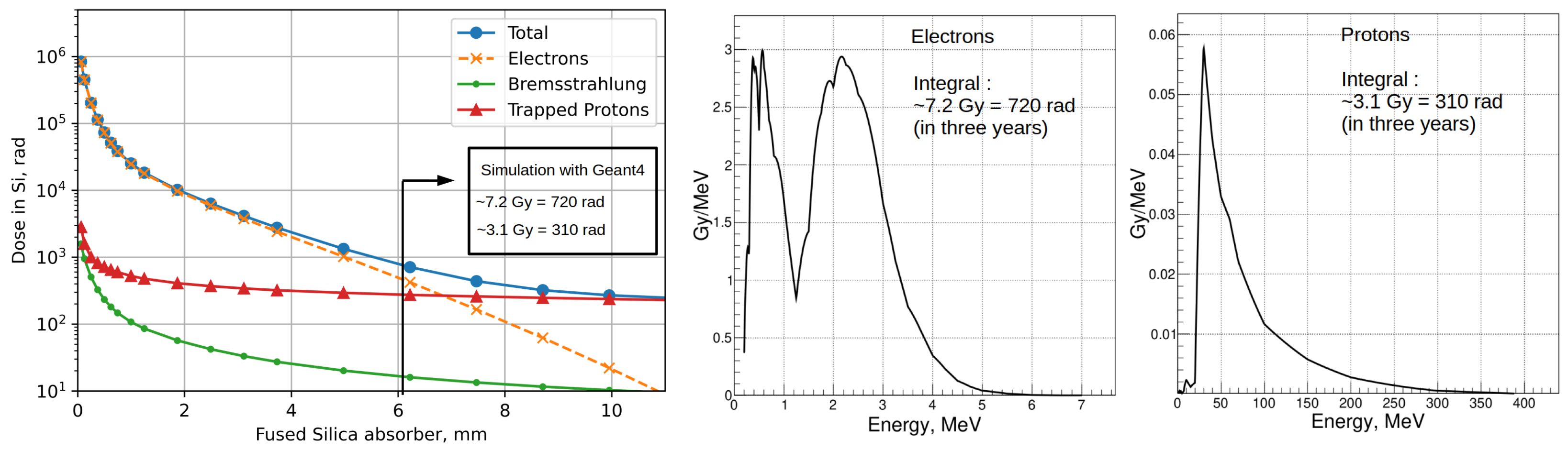
5. Dose Estimation for Terzina Telescope

The trapped electrons and protons in the Van Allen Belt are responsible for only a part of the radiation damage to the SiPMs and electronics. In this work, we do not consider solar wind protons, which can have a large impact on the total received dose. The effect will also depend on the exact time of the flight, currently foreseen to be 2026, at a time close to the maximum of the solar cycle activity.
We used SPENVIS [13] in two different ways to simulate the expected background signal on the camera. First, SPENVIS itself can estimate an accumulated dose by assuming an oversimplified geometry. We chose SPENVIS geometry with two spheres, one internal and one external. The external one is an absorber or can be considered a shield made of fused silica, and the internal one, made of silicon, is a sensitive volume, where we measure the dose. The dose in silicon with a variable layer of fused silica is shown in Figure 4. For unprotected surfaces in orbit, the radiation level is as high as ∼106 rad = 104 Gy in 3 yr of exposure.
Moreover, SPENVIS provides us with the fluxes of protons and electrons for orbits in space, trapped in the Van Allen Belt [14]. We injected the obtained SPENVIS electron and proton fluxes with an isotropic angular distribution as an input in our Geant4 [15,16] simulation of the telescope. In Figure 5, one can see the initial geometry of the Terzina telescope we consider. It consists of ∼12 mm of the corrector lens made of fused silica (no crystalline quartz), primary and secondary mirrors made of aluminum with ∼2 mm thick walls, and 2 mm of aluminum on the satellite walls. Figure 4 (right panel) shows the results of the simulation and its contribution as a function of particle energy. The estimated dose for three years of operation for only trapped protons and electrons is 7.2 Gy for electrons and 3.1 Gy for protons. (Depending on the particle type, the delivered total radiation dose causes different non-ionizing energy losses, hence causing different impacts on the SiPM DCR.) This estimation was made for the aluminum volume placed in the vicinity of the SiPM camera. The second peak in the distribution can be explained by the fact that electrons with energies higher than ∼1 MeV produce more secondary gammas with sufficient energy to reach and create a dose in the SiPM camera (Figure 4). With the same simulation, we estimated the Cherenkov background photon rate generated in the corrector lens: 181 Hz/mm produced by electrons and 0.16 Hz/mm produced by protons.
The doses obtained with the Geant4-based simulation are in agreement with SPENVIS for ∼6 mm of fused silica protection.

6. Irradiation of the SiPM with Protons

We performed the first proton irradiation test at IFJ PAN in Krakow [17] with a 50 MeV proton beam (Figure 6). The proton beam spot had a circular shape with a 35 mm diameter and homogeneity better than 5% with respect to the mean fluence. We tested SiPMs with different μ-cell sizes (25, 30, 35, 40, 50 µm) and channel sizes (1 × 1 mm2 and 3 × 3 mm2) with and without an entrance window (resin protective layer).
After every new step of irradiation, we measured the current–voltage characteristics (IV curves) to monitor increases in the DCR (Figure 6). In the reverse bias mode, the absolute voltage range was between 30 V and 50 V. In total, we performed eight irradiation sessions. After each session, the total doses received by the test samples were 1, 2, 3, 5, 7, 10, 20, and 30 Gy.
As expected, we observe an increase in the DCR with the accumulated dose. In Figure 6 (top panel), the black curve corresponds to the IV measurements taken before irradiation, and one can see a 2–3 × 10⁻⁸ A current at 42 V (∼10 V over-voltage). At a 1 Gy accumulated dose, the current for the same over-voltage has increased by two orders of magnitude (5–6 × 10⁻⁶ A) with respect to the non-irradiated case. For a 30 Gy accumulated dose, the current at 42 V bias reaches 2–3 × 10⁻⁴ A. This large increase in the DCR, even for relatively small doses, degrades the sensitivity and increases the power consumption. This preliminary study shows the importance of understanding radiation damage and the precise estimation of the dose in an orbit. The increase in the DCR due to the dose is by far dominant with respect to other backgrounds, and it is the main limiting factor for the sensitivity of the Terzina telescope. Examples of single p.e. signals before and after irradiation are shown in Figure 6 (bottom panel). The red curve corresponds to a single p.e. signal before irradiation, and the black one is the waveform taken in dark conditions after receiving a 30 Gy dose in total. The amplifier used for this measurement is AC-coupled. One can see that the signal amplitudes are compatible with single, double, and even triple p.e.’s.

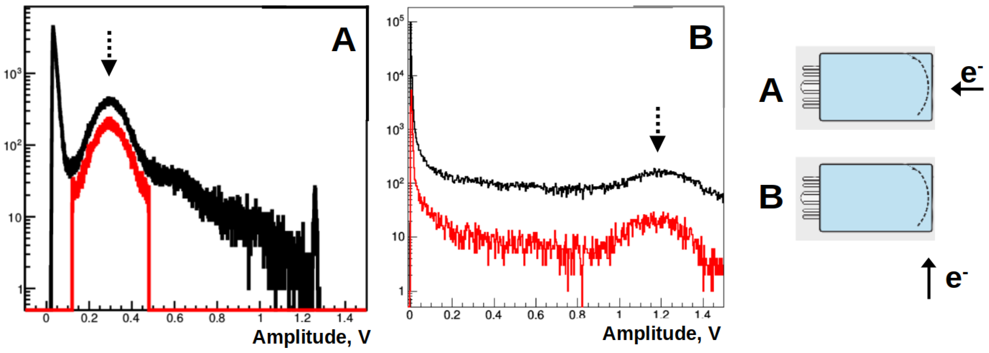
7. Background Created in a Window of a Photo Sensor

The Terzina telescope has a relatively small primary mirror; therefore, our expected signal is at the level of 7–10 p.e.’s [6]. To minimize light pollution, we require no scintillation material in the telescope. However, charged background particles (mainly electrons and positrons) can create Cherenkov light in the corrector lens or mirror substrate in the telescope. Even if a source of optical photons is located relatively far from the light sensors (see Figure 5), it can still create additional undesired noise in the SiPM camera. However, the background photons will be spread around the sensitive area (SiPM camera), making it easier to separate them from the signal. In other words, this light will be de-focalized, unlike signal photons focalized in two–three pixels.
Usually, photosensors contain a transparent window, which is a radiator of Cherenkov light. Unavoidably, PMTs suffer from this source of background. To evaluate the possible effect of this dangerous background, we used PMTs.
We carried out the test with 5.6 GeV electrons provided by the DESY [18] accelerator facility. The experimental setup contained a PMT and plastic scintillator for the trigger, installed after the PMT. We perform two tests: first (configuration A), the PMT was directly exposed to a perpendicular electron beam composed of individual electrons at a 2 kHz rate, and second (configuration B), the PMT was rotated by 90 degrees with respect to the beam (see Figure 7).
Taking into account the single-p.e. amplitude (∼15 mV), we measured 19 p.e.’s and 75 p.e.’s created by Cherenkov light for two configurations, respectively. (This is consistent with back-of-the-envelope calculations taking into account the PMT (HAMAMATSU-R7378A) quantum efficiency (bialkali photocathode material) and window refractive index (synthetic silica).) The average window thickness of the PMT and its diameter are 3 mm and 25 mm, which gives us 6 p.e.’s/mm and 3 p.e.’s/mm for the two configurations. The second configuration has twice fewer photons because half of the Cherenkov photons from the cone escape the window.
This kind of background is suppressed in the case of SiPM sensors since one can have a very thin window (resin protective layer), or it could even be removed completely.

8. Conclusions

The usage of SiPM sensors in space applications will grow in the future. They are light, with low power consumption, high PDE, and good time and spatial resolutions (see Appendix A). However, they are radiation- and temperature-sensitive devices. Therefore, the Terzina telescope design has to consider possible shields, thermostats, and SiPM annealing strategies. A description of the temperature dependence of the radiation damage annealing of a SiPM can be found in [19].
For 30 µm and 40 µm cell sizes, we measured the SiPM decay time at ∼60 ns and ∼110 ns, respectively (see Section 3). The background rate estimated using a parametric simulation of the SiPM response (see Section 4) decreases by a factor of four as a result of this notable reduction in signal duration. In Section 7, the background generated in the PMT/SiPM incoming window is explained. For ions, it is considerably more noticeable because the quantity of Cherenkov light increases squarely with the particle charge. Therefore, even a 0.1 mm thin window yields a sizable signal. We chose to employ naked sensors in order to cancel this dangerous background. Based on the study described in Section 3, Section 4, and Section 7, we decided to use a bare sensor with a 30 µm cell size.
Even in low Earth orbit, the Earth’s magnetic field loses some of its ability to shield objects from radiation. Therefore, the radiation damage will affect electronics, especially SiPMs. Geant4 [15] and SPENVIS [13] were used to assess the radiation dose levels (see Section 5) and Cherenkov light radiated by different optical elements. For only trapped protons and electrons, the dose for three years of operation is 3.1 Gy (protons) and 7.2 Gy (electrons). We calculated the Cherenkov background photon rate at 181 Hz/mm from electrons and 0.16 Hz/mm from protons using the same simulation.
In the case of crystalline materials (Si, for example), non-ionizing energy losses result in lattice dislocation and a rise in the SiPM DCR. Protons deliver significantly greater non-ionizing energy losses relative to electrons for the same total dose. Therefore, utilizing a 50 MeV proton beam supplied by the IFJ PAN radiation test facility in Krakow [17], we analyzed the rise in the SiPM DCR as a function of the total dose. A three-orders-of-magnitude increase was observed in the measured SiPM current at a 42 V bias voltage (about 10 V over-voltage) for a 3 Gy total irradiation dose (see Section 6).
Background rates due to the dose accumulated by the SiPM would become the dominant contribution during the last two years of the three-year NUSES mission (see Section 5 and Section 6).

Author Contributions

The presented material is a result of the joint work of L.B. and the NUSES Collaboration. All authors have read and agreed to the published version of the manuscript.

Funding

NUSES is a joint project of the Gran Sasso Science Institute and Thales Alenia Space Italia, funded by the Italian Government (CIPE n. 20/2019), by the Italian Minister of Economic Development and the Abruzzo Region (MISE n. F/130087/00/X38), by the Italian Space Agency (ASI n. 15/2022), and by the Swiss National Foundation (SNF grant n. 178918). This project has received funding from the European Union’s Horizon Europe Research and Innovation Programme under Grant Agreement No. 101057511 (EURO-LABS).

Data Availability Statement

No data was created for this research.

Acknowledgments

The NUSES Collaboration: R. Aloisio, C. Altomare, F. C. T. Barbato, R. Battiston, M. Bertaina, E. Bissaldi, D. Boncioli, L. Burmistrov, I. Cagnoli, M. Casolino, A. Cummings, N. D’Ambrosio, I. De Mitri, G. De Robertis, C. De Santis, A. Di Giovanni, A. Di Salvo, M. Di Santo, L. Di Venere, J. Eser, M. Fernandez Alonso, G. Fontanella, P. Fusco, S. Garbolino, F. Gargano, R. A. Giampaolo, M. Giliberti, A. Gola, F. Guarino, M. Heller, R. Iuppa, J. F. Krizmanic, S. Kusyk, A. Lega, F. Licciulli, F. Loparco, L. Lorusso, M. Mariotti, M. N. Mazziotta, S. Merzi, M. Mese, H. Miyamoto, T. Montaruli, E. Moretti, A. Nagai, R. Nicolaidis, F. Nozzoli, A. V. Olinto, D. Orlandi, G. Osteria, P. A. Palmieri, B. Panico, G. Panzarini, A. Parenti, L. Perrone, P. Picozza, R. Pillera, R. Rando, M. Rinaldi, A. Rivetti, V. Rizi, M. Ruzzarin, F. Salamida, E. Santero Mormile, V. Scherini, V. Scotti, D. Serini, I. Siddique, L. Silveri, A. Smirnov, R. Sparvoli, J. Swakoń, S. Tedesco, C. Trimarelli, D. Wróbel, L. Wu, P. Zuccon, S. C. Zugravel.

Conflicts of Interest

The authors declare no conflicts of interest.

Abbreviations

The following abbreviations are used in this manuscript:
APAfter-pulse
BoLBeginning of life
CRCosmic rays
DCRDark count rate
EASExtensive air showers
EoLEnd of life
FPAFocal plane assembly
FWHMFull-Width Half-Maximum
FWTMFull-Width Tenth-Maximum
LEOLow Earth orbit
LTANLocal Time of Ascending Node
MA-PMTMulti-Anode Photo-Multiplier Tube
NGBNight-glow background
NUSESNeutrinos and Seismic Electromagnetic Signals
NUV-HD-MTNear-Ultraviolet High-Density Metal Trench SiPM
OCTOptical cross-talk
PDEPhoton detection efficiency
p.e.Photoelectron
PMTPhoto-Multiplier Tube
SiPMSilicon Photo-Multiplier
RMSERoot mean square error
UHECRUltra-High-Energy Cosmic Rays

Appendix A

Most of the astroparticle physics missions have adopted PMTs as photosensors, while recently, a few missions have started using SiPMs. A comparison between PMTs and SiPMs is given in Table A1 with selected parameters. One can notice that SiPMs are light and low-power-consuming devices with good time and spatial resolutions with respect to PMTs. SiPMs are ageless photodetectors since their total integrated charge has practically no limits. (The total integrated charge is defined here as the total sum of SiPM output charge over its life-time. It does not depend on the operational regime (i.e., saturation or single photon) and is not related to the SiPM dynamic range.) However, we need to emphasize that SiPMs are radiation- and temperature-sensitive devices. Additionally, to detect light signals on the level of a single photon, a pre-amplifier needs to be a part of the readout chain. At room temperature, the typical SiPM dark count rate (DCR) is about ∼100 kHz/mm2, and the signals have a long falling edge defined by the quenching resistor and μ-cell capacitance.
Table A1. Photodetector comparative table.
ParameterSiPMPMT
Operation voltage<100 V∼ 1000 V
Current∼1 µA∼100 µA
Power per cm2∼1 mW∼100 mW
Weight per cm2 of sensitive area∼10 g∼100 g
Total integrated charge∼200 C
Single-p.e. time resolution<100 ps∼1 ns
Spatial resolution∼mmfew mm (1)
Photon detection efficiency @ 400 nm>50%<50%
Temperature-sensitiveyesno
Need of pre-amplifieryesoptional
Radiation resistancelowhigh
Signal FWTM (2)∼100 ns∼10 ns
(1) Multi-Anode PMTs or MA-PMTs can have small channels, 5 × 5 mm2 or 3 × 3 mm2. (2) SiPMs have a short rising edge and a very long falling edge.
The comparison between single-photoelectron (p.e.) (single p.e. (PMT) denotes a single photon that produces a primary photoelectron (p.e.) in a photocathode that reaches the first dynode of a PMT and triggers an avalanche; single p.e. (SiPM) is a single photon that triggers an avalanche) responses for a SiPM and a PMT and SiPM is shown in Figure A1. SiPMs can clearly separate single-p.e. events from the pedestal, while PMTs cannot. The PMT spectral shape is defined by the stochastic variation in the secondary electron emission, mainly from the first dynodes. The measurement for the PMT was performed with a pulsed LED (450 nm) signal. The majority of the triggers (LED pulses) contained no photons to measure a single photo-response, producing the pedestal in Figure A1(right). The simulation of the PMT, which describes the signal shape, can be found in reference [20]. The SiPM response shape is discussed in more detail in Section 4.
Figure A1. (Left): Single-p.e. response of a SiPM (amplitude spectrum). The first peak corresponds to a pedestal, the second is where only one p.e. is detected, and others are due to the primary p.e. triggering other micro-cells via either optical cross-talk or after-pulses. (Right): For comparison, we show the spectrum of a PMT with its pedestal. The simulation is shown in red, while the black line corresponds to the measurements. The single-photoelectron peak is superimposed with rare contamination due to two primary p.e.’s, as shown by the simulation of the two-p.e. response in the blue line. The number of p.e.’s on the x-axis is after the amplification of the dynode stages (the peak corresponds to a gain of 7.5 × 10⁶).
Instruments 08 00013 g0a1

References

  1. De Mitri, I. for the NUSES Collaboration. J. Phys. Conf. Ser. 2023, 2429, 012007. [Google Scholar] [CrossRef]
  2. Nuses, R.; Aloisio, C.; Altomare, F.; Barbato, R.; Battiston, M.; Bertania, E.; Bissaldi, D.; Boncioli, L.; Burmistrov, I.; Cagnoli, M.; et al. The Terzina instrument on board the NUSES space mission. In Proceedings of the 38th International Cosmic Ray Conference (ICRC2023)-Cosmic-Ray Physics (Indirect, CRI), Nagoya, Japan, 26 July–3 August 2023; Volume 444, p. 391. [Google Scholar] [CrossRef]
  3. Giovanni, A.D.; Santo, M.D.; on Behalf of the NUSES Collaboration. The NUSES space mission. In Proceedings of the 41st International Conference on High Energy physics (ICHEP2022)-Detectors for Future Facilities, R&D, Novel Techniques, Bologna, Italy, 6–13 July 2022; Volume 414, p. 354. Available online: https://pos.sissa.it/414/354 (accessed on 18 January 2024).
  4. Mazziotta, M.N.; Pillera, R. The light tracker based on scintillating fibers with SiPM readout of the Zire instrument on board the NUSES space mission. In Proceedings of the 38th International Cosmic Ray Conference (ICRC2023)-Cosmic-Ray Physics (Direct, CRD), Nagoya, Japan, 26 July–3 August 2023; Volume 444, p. 083. [Google Scholar] [CrossRef]
  5. Nuses, R.; Aloisio, A.; Altomare, B.; Barbato, B.; Battiston, B.; Bertania, B.; Bissaldi, B.; Boncioli, B.; Burmistrov, C.; Cagnoli, C.; et al. The Zire experiment on board the NUSES space mission. In Proceedings of the 38th International Cosmic Ray Conference (ICRC2023)-Cosmic-Ray Physics (Direct, CRD), Nagoya, Japan, 26 July–3 August 2023; Volume 444, p. 139. [Google Scholar] [CrossRef]
  6. Burmistrov, L.; for the NUSES Collaboration. Terzina on board NUSES: A pathfinder for EAS Cherenkov Light Detection from space. arXiv 2023, arXiv:2304.11992. [Google Scholar] [CrossRef]
  7. Olinto, A.V.; Krizmanic, J.; Adams, J.H.; Aloisio, R.; Anchordoqui, L.A.; Anzalone, A.; Bagheri, M.; Barghini, D.; Battisti, M.; Bergman, D.R.; et al. The POEMMA (Probe of Extreme Multi-Messenger Astrophysics) observatory. J. Cosmol. Astropart. Phys. 2021, 2021, 7. [Google Scholar] [CrossRef]
  8. Krizmanic, J. for the POEMMA Collaboration. POEMMA: Probe of extreme multi-messenger astrophysics. Epj Web Conf. 2019, 210, 06008, EDP Sciences. [Google Scholar] [CrossRef]
  9. Available online: https://sd.fbk.eu/en/ (accessed on 18 January 2024).
  10. Merzi, S.; Brunner, S.E.; Gola, A.; Inglese, A.; Mazzi, A.; Paternoster, G.; Penna, M.; Piemonte, C.; Ruzzarin, M. NUV-HD SiPMs with metal-filled trenches. J. Instrum. 2023, 18, P05040. [Google Scholar] [CrossRef]
  11. Gola, A.; Acerbi, F.; Capasso, M.; Marcante, M.; Mazzi, A.; Paternoster, G.; Piemonte, C.; Regazzoni, V.; Zorzi, N. NUV-Sensitive Silicon Photomultiplier Technologies Developed at Fondazione Bruno Kessler. Sensor 2019, 19, 308. [Google Scholar] [CrossRef] [PubMed]
  12. Available online: https://gitlab.com/nuses-satellite-full-simulation/terzina_wfsim (accessed on 18 January 2024).
  13. Available online: https://www.spenvis.oma.be/ (accessed on 18 January 2024).
  14. Available online: https://github.com/burmist-git/spenvis (accessed on 18 January 2024).
  15. Agostinelli, S.; Allison, J.; Amako, K.A.; Apostolakis, J.; Araujo, H.; Arce, P.; Asai, M.; Axen, D.; Banerjee, S.; Barr, G.J.N.I.; et al. GEANT4: A simulation toolkit. Nucl. Instrum. Meth. 2003, A506, 250–303. [Google Scholar] [CrossRef]
  16. Available online: https://geant4.web.cern.ch/ (accessed on 18 January 2024).
  17. Swakon, J.; Olko, P.; Adamczyk, D.; Cywicka-Jakiel, T.; Dabrowska, J.; Dulny, B.; Grzanka, L.; Horwacik, T.; Kajdrowicz, T.; Michalec, B.; et al. Facility for proton radiotherapy of eye cancer at IFJ PAN in Krakow. Radiat. Meas. 2010, 45, 1469–1471. [Google Scholar] [CrossRef]
  18. Diener, R.; Dreyling-Eschweiler, J.; Ehrlichmann, H.; Gregor, I.M.; Kötz, U.; Krämer, U.; Meyners, N.; Potylitsina-Kube, N.; Schütz, A.; Schütze, P.; et al. The DESY II Test Beam Facility. Nucl. Instruments Methods Phys. Res. Sect. Accel. Spectrometers Detect. Assoc. Equip. 2019, 922, 265–286. [Google Scholar] [CrossRef]
  19. De Angelis, N.; Kole, M.; Cadoux, F.; Hulsman, J.; Kowalski, T.; Kusyk, S.; Mianowski, S.; Rybka, D.; Stauffer, J.; Swakon, J.; et al. Temperature dependence of radiation damage annealing of Silicon Photomultipliers. Nucl. Instruments Methods Phys. Res. Sect. Accel. Spectrometers, Detect. Assoc. Equip. 2023, 1048, 167934. [Google Scholar] [CrossRef]
  20. Available online: https://github.com/burmist-git/plume_PMT_sim_USBconv (accessed on 18 January 2024).
Figure 1. (Left): Schematics of bias (red) and readout of SiPM sensors. We used 100 nF capacitor and 8 kΩ resistor. (Center): SiPM response to a 370 nm laser with ∼25 ps pulse duration (FWHM) in saturation mode (all μ-cells produce an avalanche). The waveform was recorded with a 2 GHz oscilloscope. (Right): Fit with an exponent of the SiPM signal tail. We measured 44 ns decay time for 25 µm cell size.
Instruments 08 00013 g001
Figure 2. (Left): Measurements with an LED and laser, with/without an integration sphere, of the SiPM signal decay time as a function of the μ-cell size. (Right): Rate at the fixed threshold (7 p.e.’s) as a function of the SiPM signal decay time obtained with the parametric simulation of the SiPM response.
Instruments 08 00013 g002
Figure 3. (Left top): Examples of simulated waveforms with the OCT processes only (the AP probability is set to 0). (Left bottom): Example of the waveform with the AP process only (the OCT probability is set to 0). (Right): The process history avalanche tree; the black line corresponds to OCT processes, while the red line corresponds to AP processes. For this diagram only, we set the equal probabilities of AP and OCT to 30% and the decay time constant of the μ-cell recovery time to 50 ns. Starting from the third generation, one can see the slight suppression from the right (AP) with respect to the left side (OCT). The AP/OCT probability with respect to the first generation is represented by the Z-axis.
Instruments 08 00013 g003
Figure 4. (Left): Dose due to trapped protons and electrons in silicon obtained with SPENVIS for 3 years in Terzina’s orbit vs. thickness of fused silica shielding. (Center,Right): Accumulated dose in the aluminum volume located in the vicinity of the camera and its readout electronics as a function of particle energy (for electrons and protons, respectively). The total accumulated dose in 3 years in the aluminum plane is 7.2 Gy for electrons and 3.1 Gy for protons. The electrons after ∼ 1 MeV produce more secondary gammas with high enough energy to deposit a dose in the SiPM camera.
Instruments 08 00013 g004
Figure 5. (Left): The initial geometry of the Terzina telescope. The input light (green trace) corrects its initial trajectory due to the corrector lens. Then, the primary spherical mirror reflects the photon toward the secondary mirror, which finally focalizes it on the SiPM camera. (Center): Example of background electrons with ∼6 MeV energy, producing Cherenkov light in the corrector lens and inducing dE/dx losses in the SiPM camera. The image represents a 300 μs snapshot in space. The background electrons are in red, while the Cherenkov light is in green. One can notice that these background photons have a wide angular spread. (Right): Zoom on the SiPM camera showing the aluminum volume, exactly where we count the dose deposition. One can see the camera with separate pixels made of silica.
Instruments 08 00013 g005
Figure 6. (Left): Photo of the SiPM samples installed in the IFJ PAN proton beam facility. The light spot indicates the proton beam location. (Top): The measured SiPM current as a function of the bias voltage for different accumulated doses (1 × 1 mm2, 25 µm cell, without resin). (Bottom): The waveform of the SiPM signal recorded in dark conditions and corresponding to single p.e. signals before (red) and after irradiation (black). The curve in blue shows the output SiPM signal before the breakdown voltage. It demonstrates the stability of the signal baseline.
Instruments 08 00013 g006
Figure 7. (Left): Amplitude of the signal (arrow) from the 5.6 GeV electrons impinging perpendicularly to the PMT surface. The black curve corresponds to all the measured events, while the red one requires a coincidence with a plastic scintillator, ensuring clean sample of electrons without secondaries. (Right): Amplitude of the signal from the 5.6 GeV electron impinging parallel to the PMT surface.
Instruments 08 00013 g007
Disclaimer/Publisher’s Note: The statements, opinions and data contained in all publications are solely those of the individual author(s) and contributor(s) and not of MDPI and/or the editor(s). MDPI and/or the editor(s) disclaim responsibility for any injury to people or property resulting from any ideas, methods, instructions or products referred to in the content.

