1. Introduction
The Timepix [
1] detector made its debut in space inside the International Space Station (ISS) [
2,
3], where it was used as a compact radiation monitor [
4]. The first Timepix detector exposed directly to the space environment was SATRAM (Space application of Timepix Monitor) [
5,
6] detector on board European Space Agency (ESA) satellite Proba-V [
7]. Subsequently, Timepix detectors were used on various satellites, such as CubeSat VZLUSAT-1 [
8] and RISESAT [
9]. Based on SATRAMs previous 10 years of successful operation in low earth orbit, advanced and miniaturized space radiation monitors based on Timepix3 [
10] and Timepix2 [
11] technology have been developed for the European Space Agency. Large area Timepix3 detectors (512 × 512 pixels, 55 µm pitch) were proposed for the demonstrator of the penetrating particle analyzer [
12] (mini.PAN), which is a compact magnetic spectrometer (MS) to precisely measure the cosmic ray flux, composition, spectral characteristics and directions. Mini.PAN employs position-sensitive (pixel and strip) detectors and (fast) scintillators to infer the particle type and velocity of GeV particles (and antiparticles) passing through the instrument’s magnetic field by measuring their bending angles, charge deposition and the time of flight. It will measure the properties of cosmic rays in the 100 MeV/n to 20 GeV/n energy range in deep space with unprecedented accuracy, thus providing novel results to explore the mechanisms behind the origin, acceleration, and propagation of galactic cosmic rays and solar energetic particles.
While cutting-edge hybrid pixel detectors of the Timepix family provide high spatial and temporal resolution (currently down to ∼2 ns), their implementation into space applications comes with challenges, such as their relatively large power consumption, creating heat, which has to be removed, or their high data throughput, which requires data compression and on-board processing capability. Moreover, careful electronics and chip carrier board design is required to withstand vibration and shock, and operate reliably in the radiation environments imposed by the missions. Another crucial environmental variable is temperature, which oscillates in a wide range of values (depending on the position of the spacecraft). The device needs to start up, keep working, and measure valid and correct data across a wide temperature range. Specific temperature range affecting the device depends on the mission (orbit, etc.) and the spacecraft design.
The aim of the present work is to develop a “large area” Timepix3 (area: ∼8 cm2 at 55 µm), investigate possibilities for a reduction of the power consumption, and study the impact of environmental parameters on the device performance.
2. Materials and Methods
2.1. Timepix3 Quad
Timepix3 was developed as the successor of Timepix in the Medipix3 collaboration. It features a pixel matrix of 256 × 256 pixels at a pixel pitch of 55 µm. Each of the pixels can measure simultaneously the deposited energy (ToT) and the time of arrival (ToA), the latter with precision of up to 1.6 ns. Additionally, Timepix3 implements the data-driven readout mode, where only the individual pixels triggered by ionizing radiation are read out (ToT and ToA measurements together with pixel position), while all other pixels are capable of measuring if triggered. In this mode, the minimal per-pixel dead time amounts to 19 clock cycles, which corresponds to 475 ns at the nominal 40 MHz matrix clock (see
Section 2.2). Timepix3 ASICs are hybridized with the actual radiation-sensitive sensor using flip-chip bump bonding. In flip-chip bonding, the active side of the integrated circuit is directly attached or “flipped” onto a substrate or another die, rather than being mounted upright and wire-bonded.
Ionizing radiation interacting in the sensor creates free charge carriers, which drift through the fully depleted sensor until they are collected at the electrode of the opposite charge. During the drift motion they induce currents at the pixel electrodes. These pulses are shaped and amplified in a charge-sensitive amplifier (CSA) circuit. The voltage pulses at the output of CSA are then compared to a globally adjustable threshold level (THL). Once the voltage pulse crosses THL on its upwards slope, ToA is measured and the ToT measurement is started. The latter is stopped by the pulse crossing THL on its downwards slope. The sampling of ToT and “coarse” ToA is conducted with a matrix clock of 40 MHz distributed across the entire detector matrix. This clock is derived from the external reference clock, which is generated within the readout electronics (see
Section 2.2). In order to improve the time stamping, a fast clock, created in local ring oscillators from the matrix clock, samples the time from the actual crossing of THL until the next rising edge of the coarse clock.
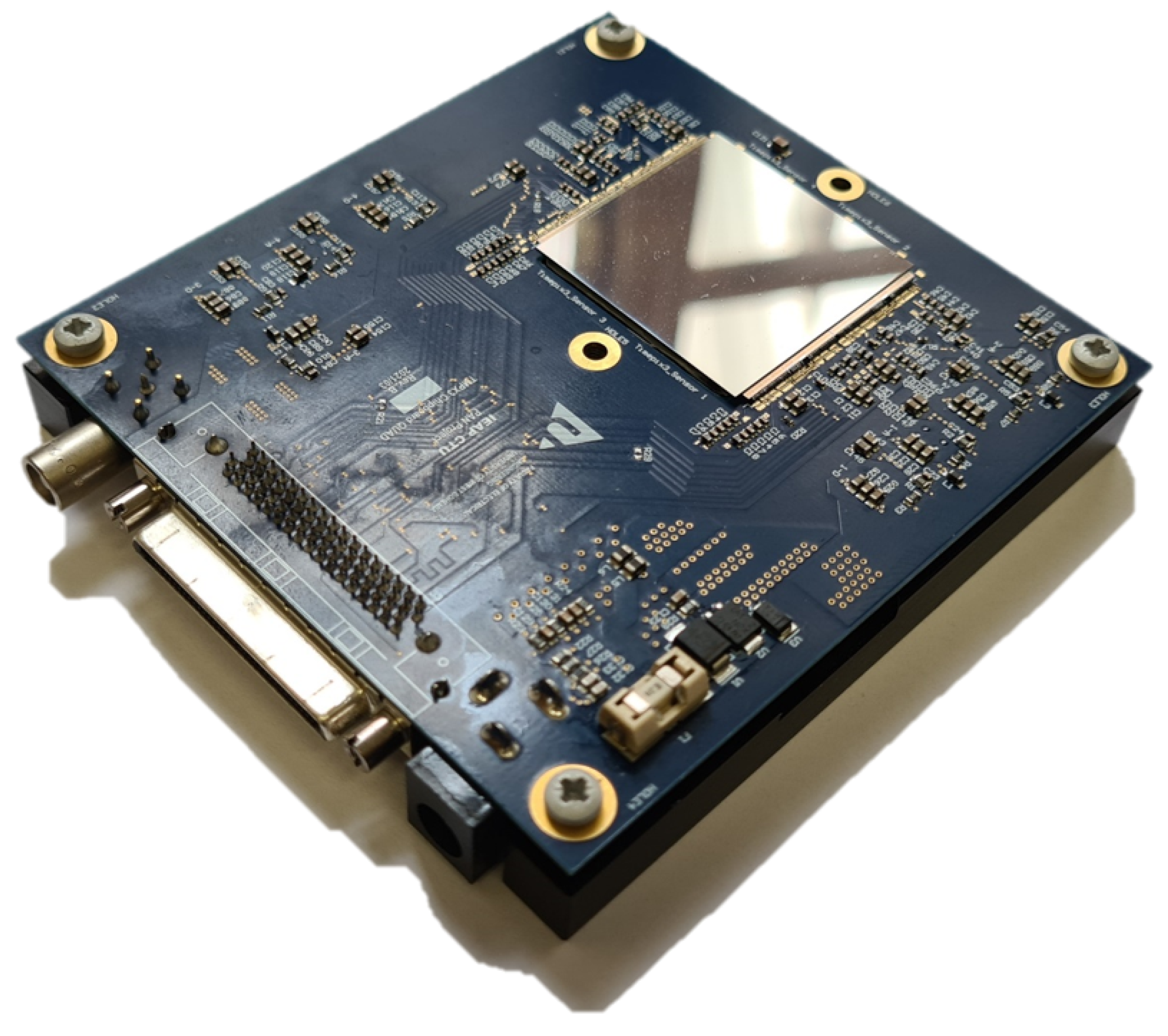
The pixel detector module, developed for the present studies, consists of 4 Timepix3 ASICs in 2 × 2 arrangement (quad), flip-chip bump bonded to a monolithic silicon sensor of 300 µm (see
Figure 1). The sensitive area covers an area of ∼7.9 cm
2 (with 512 × 512 pixels). The chipboard power supply includes a switching pre-regulator with a linear regulator to ensure precise voltage for the chips. The chips are glued to an aluminum heat sink to help manage and dissipate the heat generated during operation. In the current version, we use two data lines per chip (20 MHit/s/chip), so that the maximum data rate for the entire quad is 80 MHit/s.
2.2. Low-Power Modes of Timepix3 Quad
In particular, applications in space or in a vacuum, where power budgets and heat removal options are limited, low-power (LP) operation can be paramount. A previous work [
13] outlines possibilities to reduce the power consumption of Timepix3 significantly and demonstrates that, in the best case, the single chip was operated at 250 mW. The power consumption of the Timepix3 detector can be divided into two primary components: the consumption of the analog part and the digital part.
The nominal power consumption of the analog part is 800 mW per chip. This power consumption was reduced to 55 mW per chip by tuning the digital-to-analog converter (DAC) settings. Changes to the main DAC registers responsible for the power consumption are shown in
Table 1.
Power consumption on the digital part can be reduced by decreasing the clock frequency. Timepix3 has two main clock domains: system clock and matrix clock. The system clock is generated externally in the Katherine readout [
14], while the matrix clock is generated inside the Timepix3 chip. The system clock is used by the Timepix3 peripherals like the Bus Controller and the Command Controller. These peripherals are only a small part of the Timepix3 chip, so the influence of the system clock on the detector’s power consumption is minor. The matrix clock is used for the ToT/ToA measurements and has a major influence on power consumption.
In default mode, the matrix clock is derived from the internal Phase-Locked Loop (PLL) and this PLL needs an external reference clock (ClkInRefPLL) to be 40 MHz to function properly. This external reference clock is also provided by the Katherine readout. However, the PLL can be bypassed and the matrix clock can be fed directly by the reference clock. Bypassing the PLL and generating a matrix clock directly from the reference clock allows us to find a suitable clock frequency to meet our needs for performance and power consumption. The nominal power consumption of the digital part is 600 mW per chip. By lowering the matrix clock frequency (in this case to 5 MHz) we reduced the power consumption to 150 mW per chip. The matrix clock also influences the timing properties of the detector (ToA measurements). The fast clock (640 MHz) used for the fine ToA is generated internally from the matrix clock and is available only if we use the default value of the matrix clock (40 MHz). Without the fine ToA, the timing properties are limited by the sampling frequency of the clock externally fed to the ASIC. Moreover, since the clock frequency also determines the readout time, the per-pixel dead time increases.
For all presented measurements a custom-built improved Katherine readout was used with in-house built control software.
We consider dynamic switching between modes in order to best adapt the device performance to the available platform resources. For example, a user-specified average power budget could be achieved by varying between different modes and taking data at different temporal resolutions and readout speeds. We define the following 4 Timepix3 power modes (1 normal, 3 LP):
Normal mode—full performance (standard DACs settings, default 40 MHz matrix clock). The nominal power consumption is ≈6 W;
Analog LP mode—the DACs are set to LP mode, while the default 40 MHz matrix clock is used. The power consumption is ≈3 W;
LP20—The DACs are set to LP mode (analog LP) and the matrix clock is reduced to 20 MHz. The power consumption is ≈2.2 W;
LP5—Same as LP20, but at a matrix clock of 5 MHz. The power consumption is lower than ≈2 W.
To reduce the impact of the lower sampling frequency on the energy measurement performance (sampling error) at lower matrix clock frequencies, the IKrum DAC was set at 10 and 5 for LP20 and LP5, respectively, thus, elongating the analog pulses.
Measurement of the real Timepix3 quad power consumption in digital LP modes has revealed higher values compared to the extrapolation of four single Timepix3 chipboards (see
Table 2). This can be explained by an overhead in the losses on the chipboard voltage regulators, which do not work as efficiently in low-power modes. It should be noted that future improved hardware chipboard design might overcome this issue.
2.3. Experimental Setups
The functionality of the detector was tested with laboratory sources and in charged particle beams at CERN’s super-proton-synchrotron (SPS) and the Danish Center for Particle Therapy (DCPT). At SPS, the 120 GeV hadron beam (90% pions), we focused on investigating the difference between normal and analog low-power modes. At DCPT, a more detailed study was conducted using proton beams of 80 MeV and 240 MeV. Here, the detector response was determined at all predefined power settings (normal, analog LP, LP20, and LP5). Since the data rate in the center of the clinical proton beam exceeded the capabilities of the chip in the data-driven mode, the measurements were taken at a lateral displacement of 12 cm. In the particle beams, measurements were taken at different impact angles in the range from 0 (perpendicular) to 90 degrees with respect to the sensor normal. For thermal tests, the detector was calibrated in a laboratory with a chip temperature of +50 °C (±1 °C) (corresponds to an ambient temperature of ∼25 °C). The detector was then placed together with an 241Am -source (peak energy 59.6 keV) of 300 kBq inside a climate chamber (Votsch VCV 7060 - 5, Vötsch Industrietechnik GmbH; Beethovenstrasse 34, Balingen-Frommern 72336, Germany). The detector was connected to the Katherine readout, positioned outside the climate chamber (the readout electronics remained unaffected by temperature changes), enabling us to measure only the detector’s response to temperature variations. Measurements were taken for three power modes (normal, LP20, LP5) in an ambient temperature range of −20 °C–+50 °C. Before each measurement, we waited until thermal equilibrium was achieved. During all performed tests, the following environment variables were monitored: the ambient temperature, the temperature of the used Timepix3 detectors, and the temperature on the heat sink.
All measurements were taken using the data-driven mode of Timepix3. The sensor was fully depleted using a bias voltage of 60 V.
2.4. Data Analysis
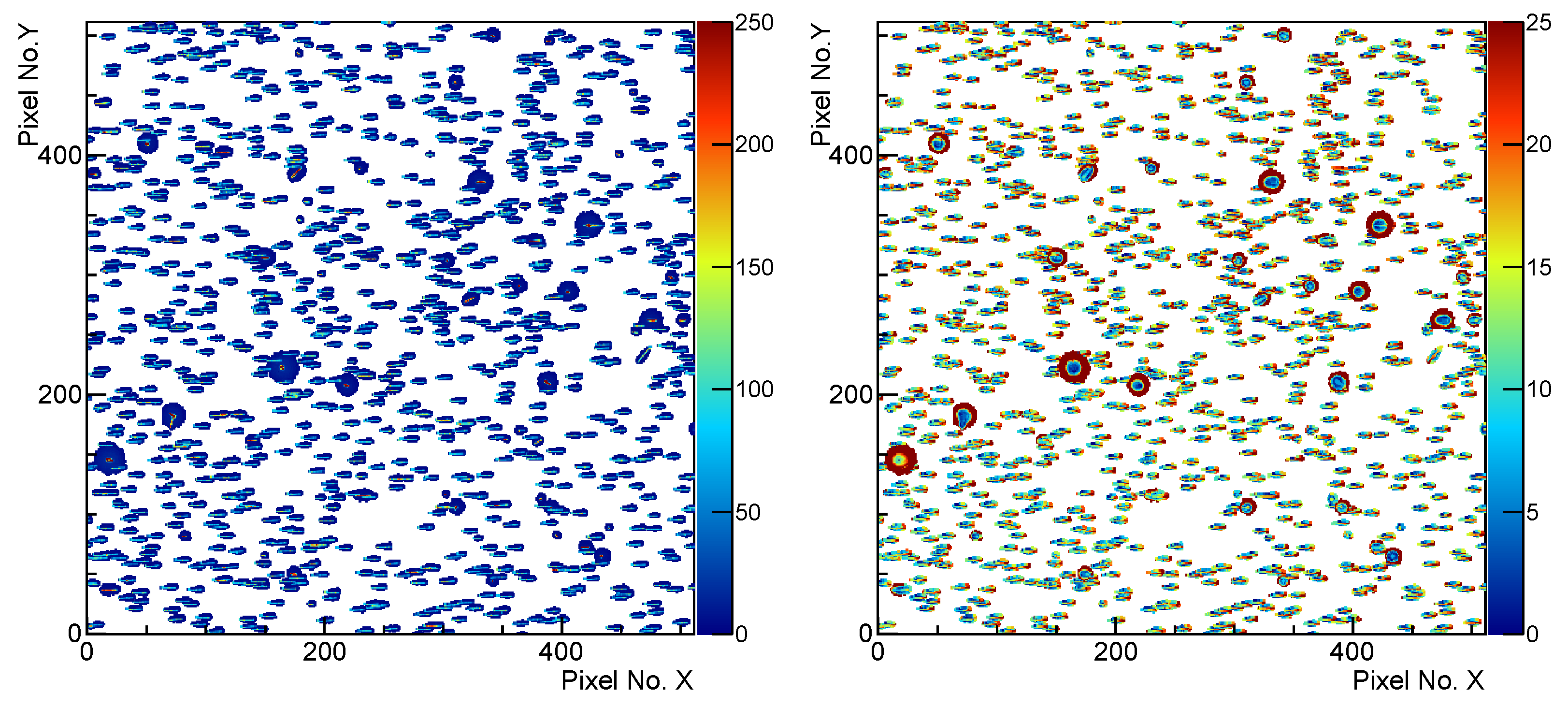
The data are sent off the chip as a list of partially temporally unsorted pixel hits. These are then grouped into so-called “clusters” using temporal coincidence and spatial neighborhood conditions. For the present evaluations, a floating coincidence time window of 200 ns was used.
Figure 2 shows a set of 1000 clusters measured at DCPT with 80 MeV protons.
For each found cluster the following features are calculated:
The deposited energy is defined as the sum of the energies measured in the pixels;
The cluster size is defined as the number of pixels within a cluster;
The cluster drift time difference is defined as the difference of the minimal and maximal timestamp measured within a cluster.
3. Results
3.1. Impact of Low-Power Settings on the Energy Measurement
The ToT-to-energy calibration was conducted with X-ray fluorescence lines of known energy and the 59.6 keV
-line from a
241Am source, as described in [
14]. A stable noise-free operation at a threshold (THL) of 2.75 keV was found. For further measurements and anticipating the temperature effects, it has been conservatively set at THL = 4 keV.
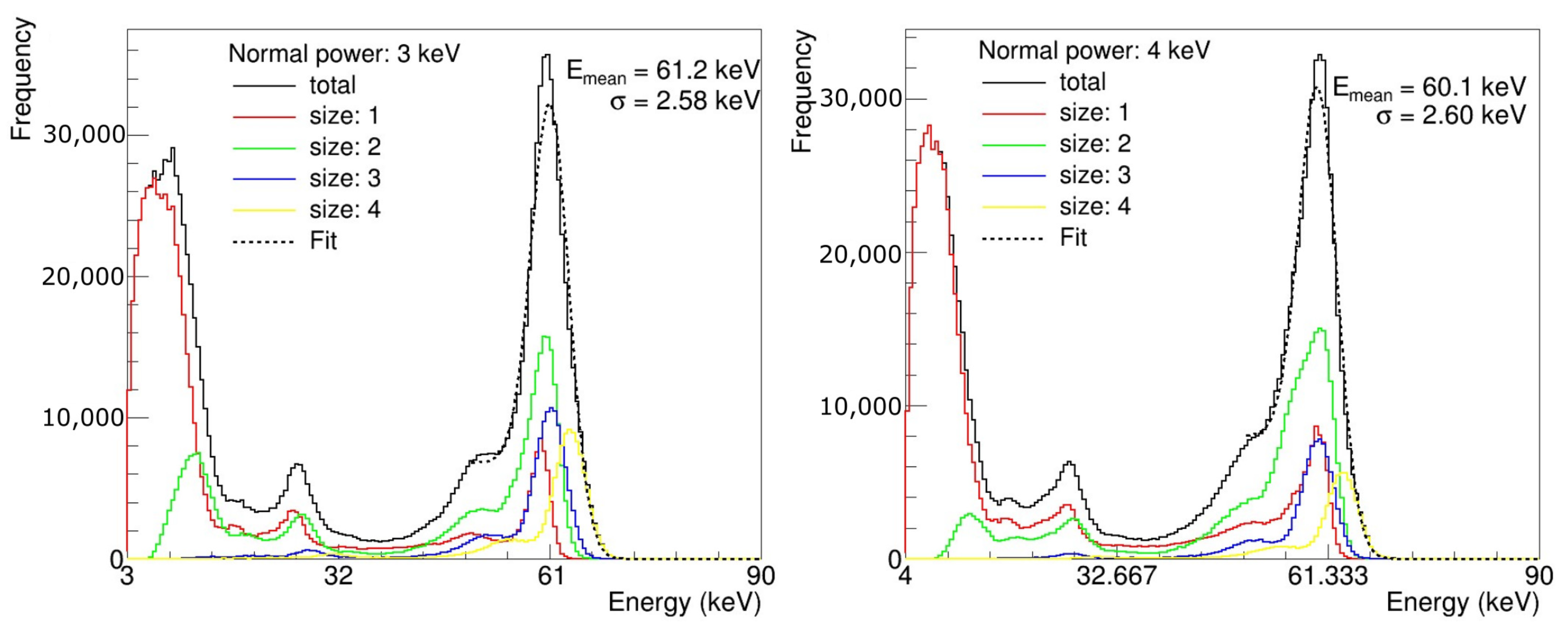
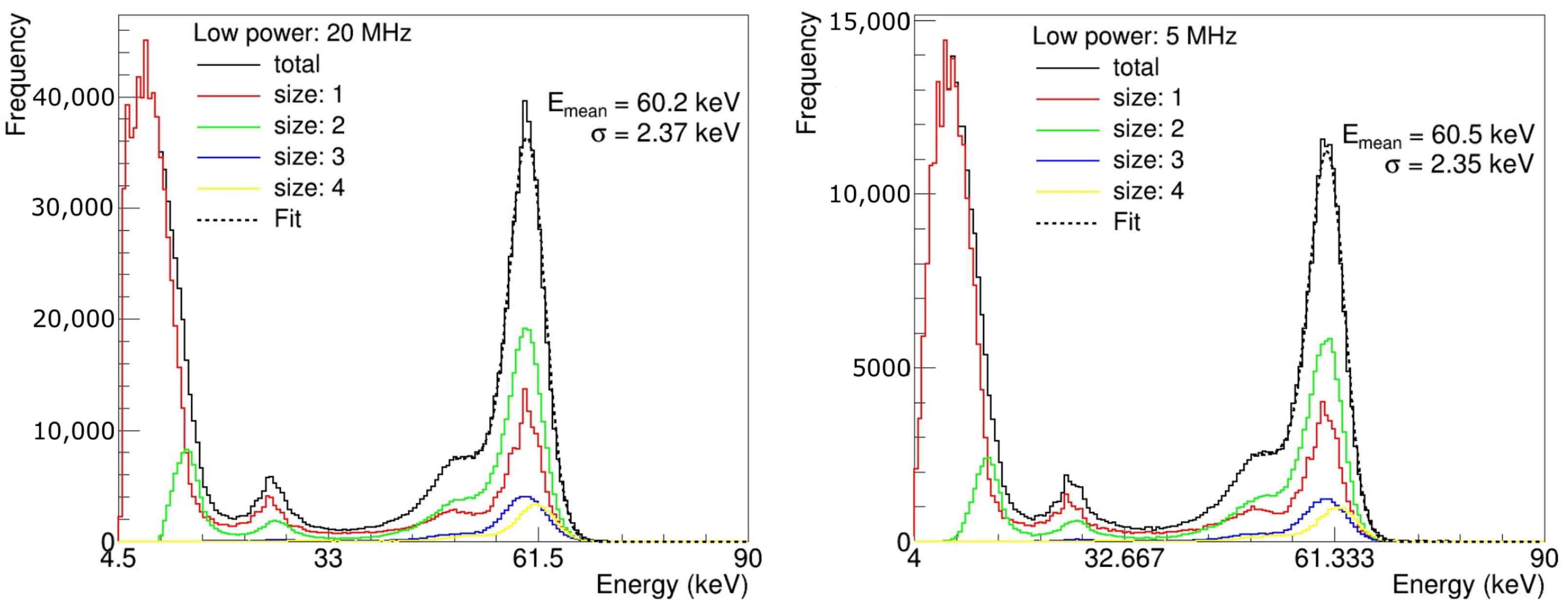
The calibrated energy spectra of a
241Am source are shown in
Figure 3 and
Figure 4 for normal mode and low-power modes, respectively. Different colors give the spectra for different cluster sizes. While the best resolution is achievable utilizing single-pixel clusters, we determine the overall energy resolution by fitting the 59.6 keV peak with a Gaussian curve sitting on an error-function:
where the Gaussian amplitude
A, the error-function height
B, the mean energy
and the energy resolution
were the fit parameters.
Table 3 summarizes the energy resolutions found for the different power modes. Overall, consistent results were found at the different settings.
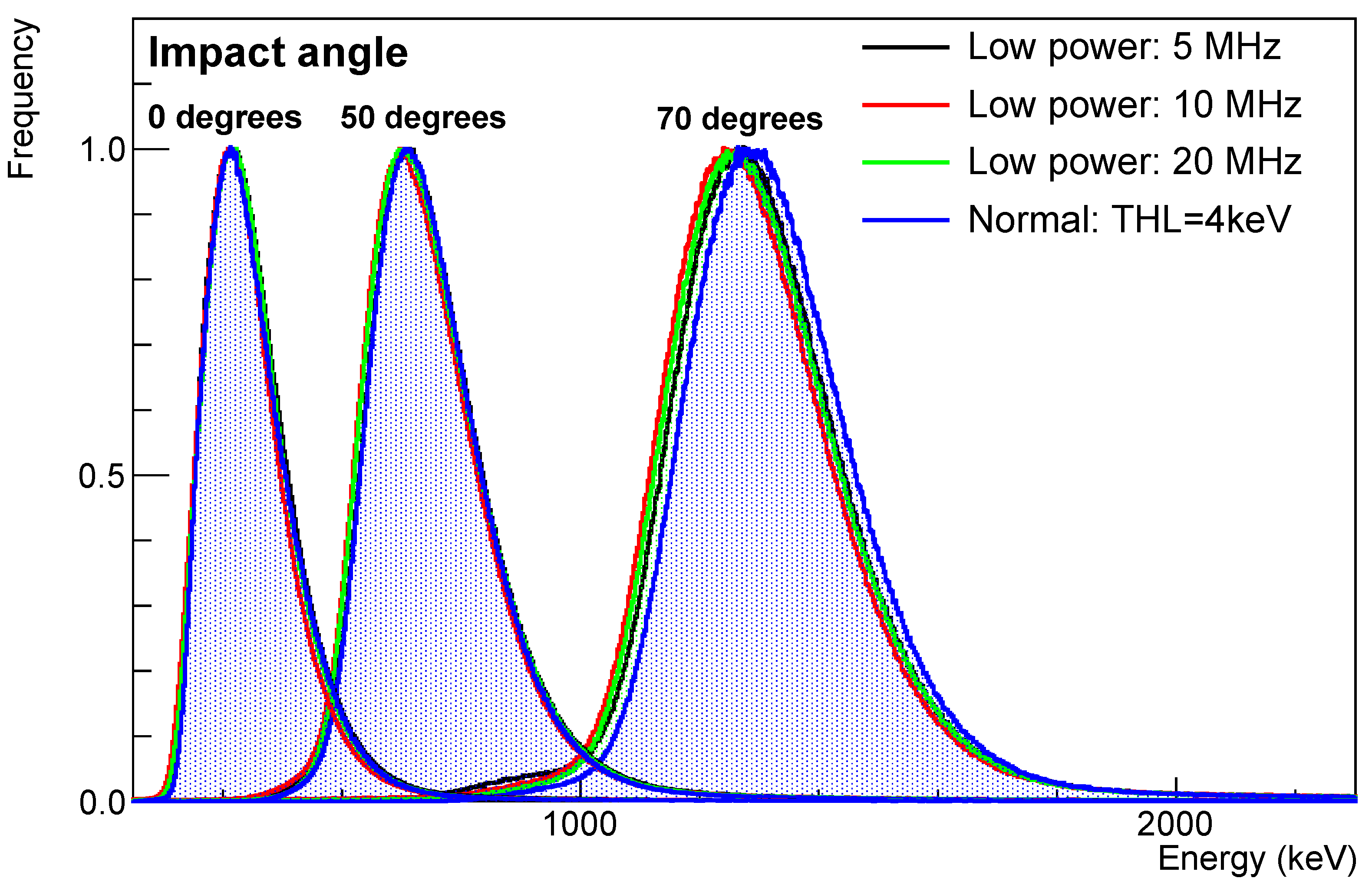
The energy responses from the proton test are shown in
Figure 5. The same behavior was found for the measurement with pions at SPS. In this measurement campaign, different energy deposition in the sensor was achieved by measurement at particle impact angles of 0, 50, and 70 degrees with respect to the sensor normal. For a thin absorber, the physics of the energy deposition are described by a Landau curve, which is, however, convolved with a Gaussian smearing describing the energy resolution of the detector (0 degree impact angle). At both higher impact angles (50 and 70 degrees) the sensor cannot be regarded as a thin layer anymore. Consequently, the tail towards higher energy is suppressed while the overall expected spectrum shape becomes Gaussian-like. From the presented measurements, we can conclude that the investigated LP modes do not have a significant effect on the overall energy measurement.
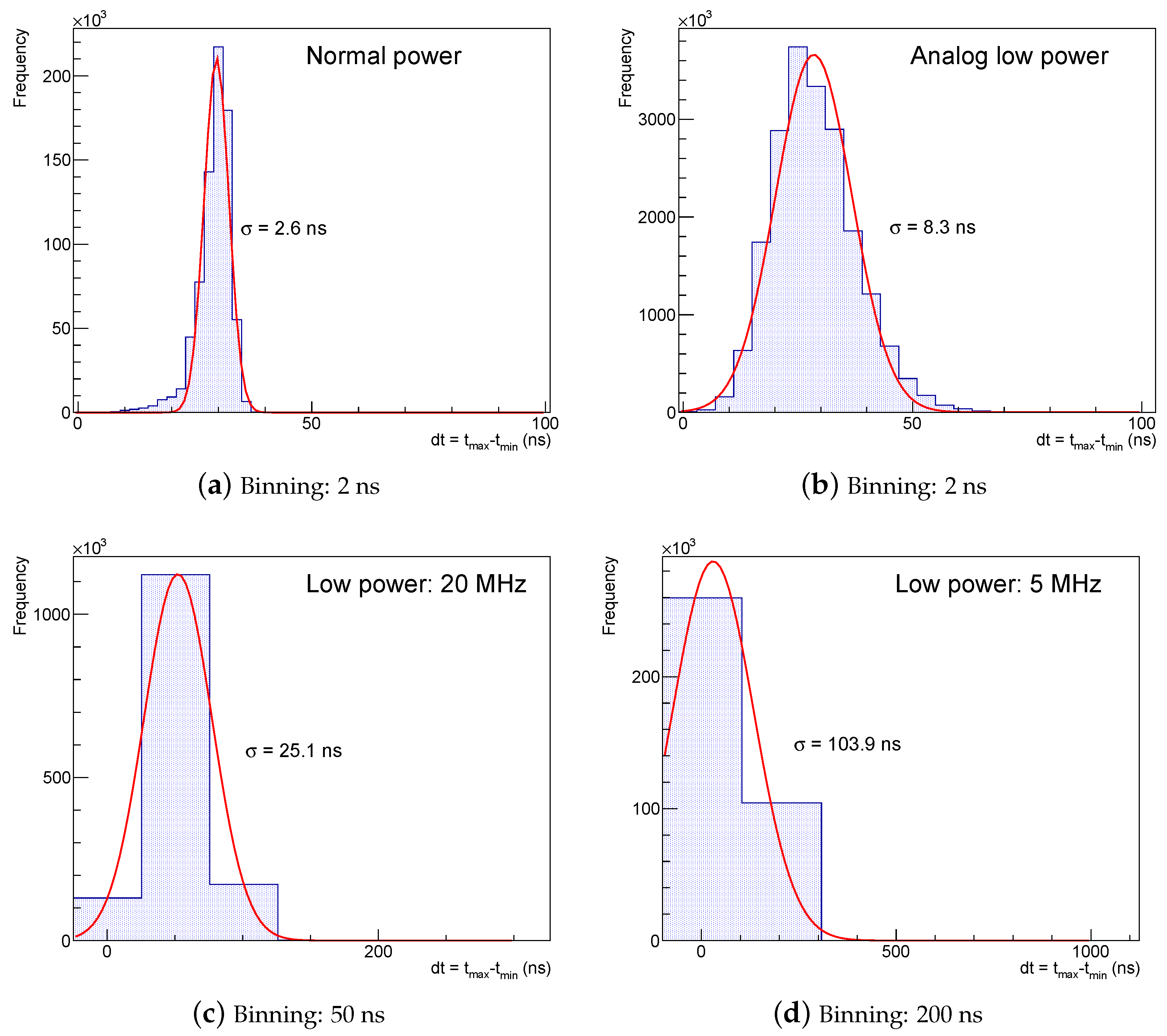
3.2. Impact of the Low-Power Settings on the Time Resolution
To determine the performance of the time measurement, we use data taken at a proton energy of 240 MeV and a 70-degree impact angle. We then measure the drift time across the entire sensor by calculating the difference of the maximal time differences within a cluster (see, e.g., [
15] for a discussion about the drift time studies with Timepix3). The measured time distributions are shown in
Figure 6 for the different modes investigated. The peaks were fitted with a Gaussian distribution to determine the widths
. Since the time is measured twice (maximum and minimum time), the real time resolution of the detector can be calculated as
. The determined time resolution for the different modes is given in
Table 4.
While at the standard clock (normal, analog low-power) the time resolution is given by the pulse shaping, in digital low power, the sampling frequency determines the achievable resolution. At 20 and 10 MHz, the measured values, i.e., 18 ns and 28 ns, are consistent with the resolutions calculated from the time binning as with the time stamping granularity , which are 14 ns and 29 ns, respectively. At 5 MHz, the measured resolution is slightly worse than the predicted one (74 ns versus 58 ns). This is caused by the frequency being at the edge of the supported range of the clock generator adding an additional clock instability.
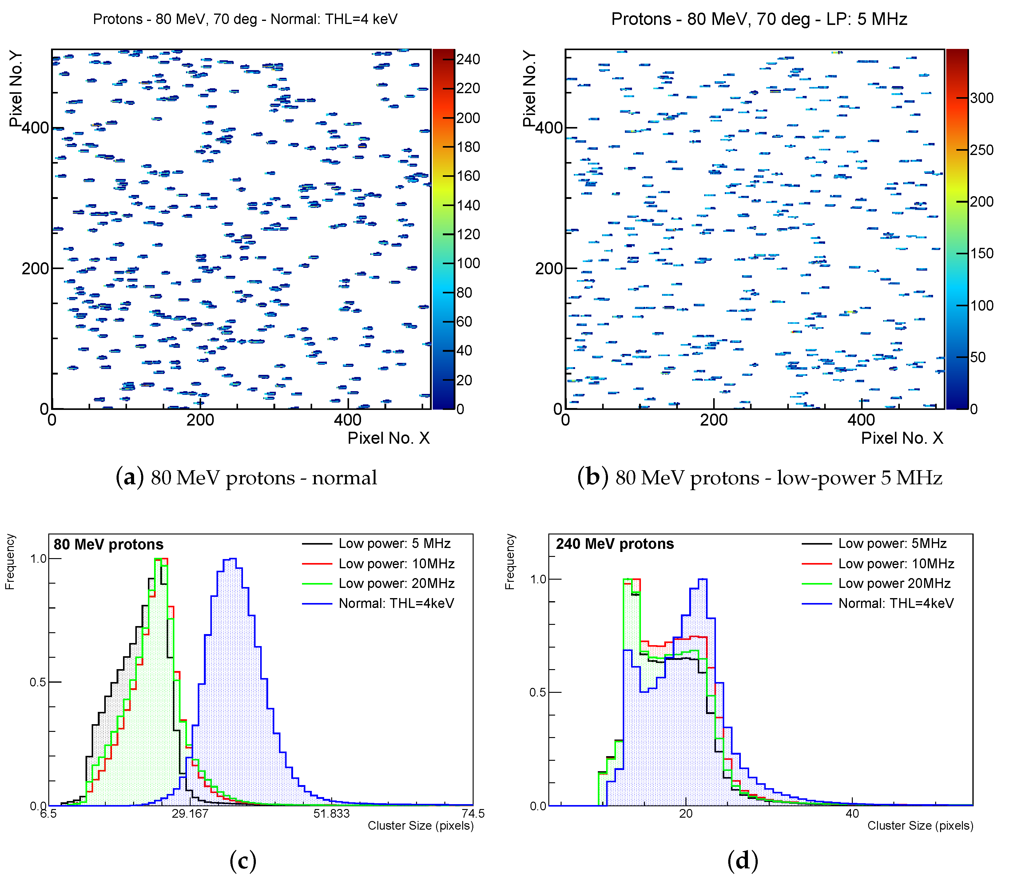
3.3. Impact of the Low-Power Settings on the Cluster Shape
For completeness, we present a qualitative comparison of clusters measured in normal (at different THL) and low-power settings (
Figure 7a,b). A quantitative description is shown by the cluster size distributions for the 80 MeV and 240 MeV proton measurements at a 70-degree impact angle in
Figure 7c,d, respectively. Overall, the cluster sizes decrease at analog low-power DAC settings. This effect is stronger for clusters with high stopping power (see the 80 MeV data sets) and is not visible at lower stopping power. This difference can be explained by looking at the behavior of the Krummenacher circuit in the pixel electronics. The capacitor in the amplification circuit is discharged at a constant rate
. The charge loss until the pulse reaches the peak position
can thus be estimated as
. Since the rise time in the low-power modes
is slower than at normal settings
, charge losses are higher and the pulses in the periphery of the tracks that have energy just above the threshold are lost in LP settings. While this cluster shape difference in the different modes does not impact the overall performance of the detector, it should be carefully considered when using already trained neural networks used for particle identification [
16].
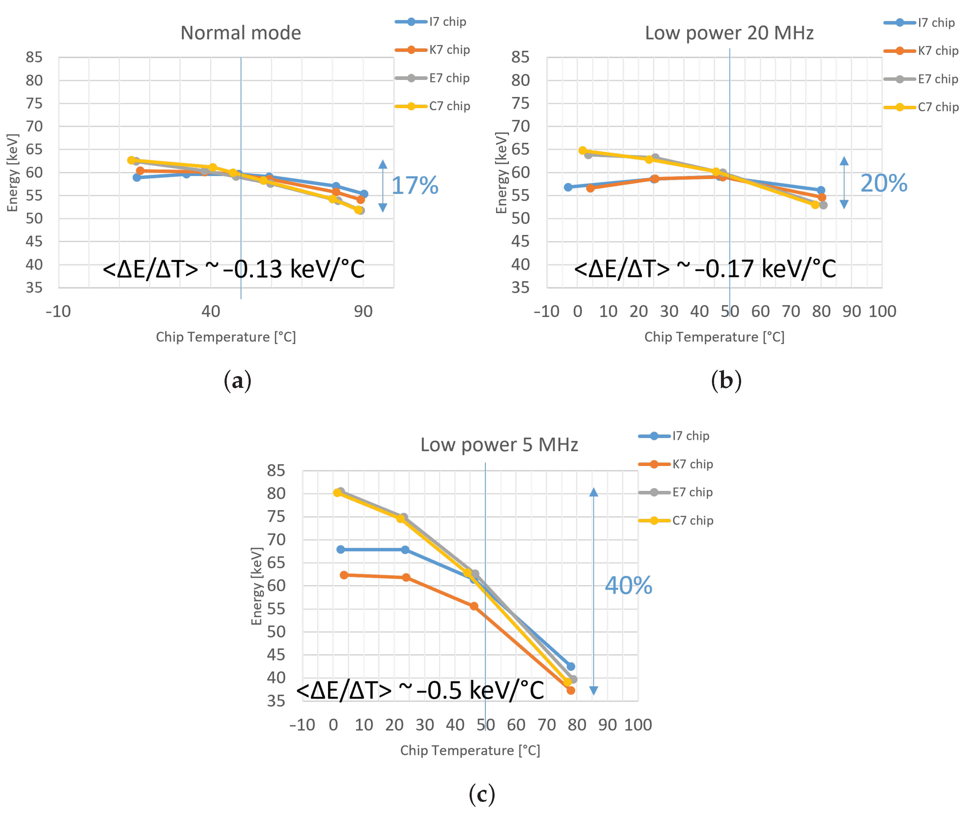
3.4. Effect of the Temperature on the Energy Measurement
Figure 8 shows the measured
241Am
-peak position at different chip temperatures. For these measurements, the ambient temperature range was −20 °C– 50 °C. In all modes, the peak positions move towards lower energy at increasing temperatures. However, the peak shift at digital low-power settings shows a stronger dependency on chip temperature with a larger variation amongst the chips. Therefore, we recommend a determination of the calibration coefficients at different temperatures. The shift of measured energy based on temperature change was also demonstrated in papers [
17,
18], where a single Timepix3 chip in normal mode was tested.
4. Conclusions
The manuscript presented the characterization of a large area Timepix3 detector with a 300 µm-thick silicon sensor, particularly for measurement in space. The requirements for cooling and limited energy resources were mitigated by implementing different power consumption modes. Since available resources can change during the lifetime of a mission, it is possible to dynamically change between these modes.
Thermal tests show that the measured energy is dependent on temperature and this dependency varies with different DACs settings and used clock frequency. The behavior between every single chip on the Timepix3 Quad varies by a small margin. This variation is stronger for low-power modes with a reduced matrix clock (very noticeable for LP5). In particular, the temperature dependence in the low-power modes is not negligible. Thus, in applications where the temperature could change more than ±5 °C from the calibration temperature, we recommend prior calibration at different temperatures and selecting the appropriate calibration coefficients.
A custom-built readout was used to test the functionality of the detector and its response to a 120 GeV/c hadron beam at the Super-Proton-Synchrotron (SPS) at CERN and to protons of 80 and 240 MeV at the Danish Center for Proton Therapy (DCPT). The power consumption of 6 W with standard settings was reduced to 3 W by changing the Timepix3 DACs. While these changes did not affect the energy measurement resolution, the time stamping precision was reduced from 1.8 ns to 5.9 ns due to the slower shaping of the rising edge of the analog pulse. Further reduction of the power consumption was achieved by reducing the matrix clock. At a matrix clock of 5 MHz, we achieved a power consumption of 2 W. While the sampling frequency effect on the energy measurement was successfully mitigated by adjustment of the pulse length (through the chips’ IKrum DAC), the time stamping precision is determined by the used matrix clock in the deep digital low-power modes (LP20, LP5).
Author Contributions
Project administration and Funding acquisition G.A., P.A. and X.W.; Investigation, Resources P.B. (Pavel Broulim) and L.P.; Investigation, software P.B. (Petr Burian); Formal analysis, Writing—review & editing, Project administration and Funding acquisition B.B.; Formal analysis, Resources P.S.; Investigation, Writing—original draft M.F.; Resources M.S.; Validation D.S. All authors have read and agreed to the published version of the manuscript.
Funding
This project has received funding from the European Union’s Horizon 2020 research and innovation programme under grant agreement No 862044. This work has been done using the INSPIRE Research Infrastructures and is part of a project that has received funding from the European Union’s Horizon 2020 research and innovation programme under grant agreement No 730983. Martin Farkaš received funding from the internal project to support student scientific conferences SVK1-2023-005 and project SGS-2021-005: Research, development and implementation of modern electronic and information systems.
Institutional Review Board Statement
Not applicable.
Informed Consent Statement
Not applicable.
Data Availability Statement
The data presented in this study are available on request from the corresponding author.
Acknowledgments
The work was carried out in the Medipix collaboration. Full Authorlist of the PAN Collaboration: Giovanni Ambrosi (Istituto Nazionale di Fisica Nucleare, Italy), Philipp Azzarello2, Mattia Barbanera6, Benedikt Bergmann3, Bruna Bertucci1, Pavel Broulim4, Petr Burian3,4, Frank Raphael Cadoux2, Michael Campbell5, Mirco Caprai6, Fabio Cossio6, Matteo Duranti6, Yannick Favre2, Stefan Gohl3, Maura Graziani1, Tomoya Iizawa2, Maria Ionica6, Merlin Kole2, Daniel La Marra2, Edoardo Mancini1, Petr Manek3, Lorenzo Mussolin1, Mercedes Paniccia2, Stanislav Pospisil3, Lukáš Pušman4, Petr Smolyanskiy3, Jerome Stauffer2, Daniil Sukhonos2, Pierre Alexandre Thonet5, Nicola Tomassetti1, Xin Wu2, Pengwei Xie2. 1 Universita e INFN, Perugia, Italy; 2 Universite de Geneve, Switzerland; 3 Institute of Experimental and Applied Physics, CTU, Czech Republic; 4 University of West Bohemia, Czech Republic; 5 CERN, Switzerland; 6 Istituto Nazionale di Fisica Nucleare, Italy.
Conflicts of Interest
The funders had no role in the design of the study; in the collection, analyses, or interpretation of data; in the writing of the manuscript; or in the decision to publish the results.
Abbreviations
The following abbreviations are used in this manuscript:
| LP | Low-Power |
| PAN | Penetrating Particle Analyzer |
| DAC | Digital to Analog Converter |
| ToT | Time over Threshold |
| ToA | Time of Arrival |
| PLL | Phase-Locked Loop |
Appendix A. The Full Set of the Timepix3 Analog DAC Settings in HP and LP Mode
Table A1.
Time stamping precision for Timepix3 Quad in normal mode and LP modes.
Table A1.
Time stamping precision for Timepix3 Quad in normal mode and LP modes.
| DAC | Normal | Low-Power |
|---|
| PreampOn | 128 | 8 |
| PreampOff | 8 | 8 |
| VPreamp | 128 | 128 |
| Ikrum | 15 | 10 (LP20) and 5 (LP5) |
| Vfbk | 164 | 128 |
| DiscS1On | 100 | 8 |
| DiscS1Off | 8 | 8 |
| DiscS2On | 128 | 8 |
| DiscS2Off | 8 | 8 |
| Pixel | 128 | 20 |
| TpBufferIn | 128 | 128 |
| TpBufferOut | 128 | 128 |
| VtpCoarse | 128 | 128 |
| VtpFine | 256 | 256 |
| CpPLL | 128 | 128 |
| PLLVcntrl | 128 | 128 |
References
- Llopart, X.; Ballabriga, R.; Campbell, M.; Tlustos, L.; Wong, W. Timepix, a 65k programmable pixel readout chip for arrival time, energy and/or photon counting measurements. Nucl. Inst. Meth. A 2007, 581, 485–494. [Google Scholar] [CrossRef]
- Stoffle, N.; Pinsky, L.; Kroupa, M.; Hoang, S.; Idarraga, J.; Amberboy, C.; Rios, R.; Hauss, J.; Keller, J.; Bahadori, A.; et al. Timepix-based radiation environment monitor measurements aboard the International Space Station. Nucl. Instrum. Methods A 2015, 782, 143–148. [Google Scholar] [CrossRef]
- Kroupa, M.; Bahadori, A.; Campbell-Ricketts, T.; Empl, A.; Hoang, S.; Idarraga-Munoz, J.; Rios, R.; Semones, E.; Stoffle, N.; Tlustos, L.; et al. A semiconductor radiation imaging pixel detector for space radiation dosimetry. Life Sci. Space Res. 2015, 6, 69–78. [Google Scholar] [CrossRef] [PubMed]
- Turecek, D.; Pinsky, L.; Jakubek, J.; Vykydal, Z.; Stoffle, N.; Pospisil, S. Small Dosimeter based on Timepix device for International Space Station. J. Instrum. 2011, 6, C12037. [Google Scholar] [CrossRef]
- Granja, C.; Polansky, S.; Vykydal, Z.; Pospisil, S.; Owens, A.; Kozacek, Z.; Mellab, K.; Simcak, M. The SATRAM Timepix spacecraft payload in open space on board the Proba-V satellite for wide range radiation monitoring in LEO orbit. Planet. Space Sci. 2016, 125, 114–129. [Google Scholar] [CrossRef]
- Gohl, S.; Bergmann, B.; Evans, H.; Nieminen, P.; Owens, A.; Posipsil, S. Study of the radiation fields in LEO with the Space Application of Timepix Radiation Monitor (SATRAM). Adv. Space Res. 2019, 63, 1646–1660. [Google Scholar] [CrossRef]
- Proba-V Carrying Radiation Detector from CERN to Space. Available online: http://www.esa.int/Our_Activities/Technology/Proba_Missions/Proba-V_carrying_radiation_detector_from_CERN_to_space (accessed on 20 December 2023).
- Baca, T.; Jilek, M.; Vertat, I.; Urban, M.; Nentvich, O.; Filgas, R.; Granja, C.; Inneman, A.; Daniel, V. Timepix in LEO Orbit onboard the VZLUSAT-1 Nanosatellite: 1-year of Space Radiation Dosimetry Measurements. J. Instrum. 2018, 13, C11010. [Google Scholar] [CrossRef]
- Filgas, R. et al. RISEPix—A Timepix-based radiation monitor telescope onboard the RISESAT satellite. Astron. Nachrichten 2019, 340, 674–680. [Google Scholar] [CrossRef]
- Poikela, T.; Plosila, J.; Westerlund, T.; Campbell, M.; De Gaspari, M.; Llopart, X.; Gromov, V.; Kluit, R.; Van Beuzekom, M.; Zappon, F.; et al. Timepix3: A 65K channel hybrid pixel readout chip with simultaneous ToA/ToT and sparse readout. J. Instrum. 2014, 9, C05013. [Google Scholar] [CrossRef]
- Wong, W.S.; Alozy, J.; Ballabriga, R.; Campbell, M.; Kremastiotis, I.; Llopart, X.; Poikela, T.; Sriskaran, V.; Tlustos, L.; Turecek, D. Introducing Timepix2, a frame-based pixel detector readout ASIC measuring energy deposition and arrival time. Radiat. Meas. 2020, 131, 106230. [Google Scholar] [CrossRef]
- Wu, X.; Ambrosi, G.; Azzarello, P.; Bergmann, B.; Bertucci, B.; Cadoux, F.; Campbell, M.; Duranti, M.; Ionica, M.; Kole, M.; et al. Penetrating particle analyzer (pan). Adv. Space Res. 2019, 63, 2672–2682. [Google Scholar] [CrossRef]
- Burian, P.; Broulim, P.; Bergmann, B. Study of Power Consumption of Timepix3 Detector. J. Instrum. 2019, 14, C01001. [Google Scholar] [CrossRef]
- Burian, P.; Broulim, P.; Jara, M.; Georgiev, V.; Bergmann, B. Katherine: Ethernet Embedded Readout Interface for Timepix3. J. Instrum. 2017, 12, C11001. [Google Scholar] [CrossRef]
- Bergmann, B.; Pichotka, M.; Pospisil, S.; Vycpalek, J.; Burian, P.; Broulim, P.; Jakubek, J. 3D track reconstruction capability of a silicon hybrid active pixel detector. Eur. Phys. J. C 2017, 77, 421. [Google Scholar] [CrossRef]
- Ruffenach, M.; Bourdarie, S.; Bergmann, B.; Gohl, S.; Mekki, J.; Vaillé, J. A New Technique Based on Convolutional Neural Networks to Measure the Energy of Protons and Electrons With a Single Timepix Detector. IEEE Trans. Nucl. Sci. 2021, 68, 1746–1753. [Google Scholar] [CrossRef]
- Urban, M.; Nentvich, O.; Marek, L.; Hudec, R.; Sieger, L. Timepix3: Temperature Influence on Radiation Energy Measurement with Si Sensor. Sensors 2023, 23, 2201. [Google Scholar] [CrossRef] [PubMed]
- Urban, M.; Doubravová, D. Timepix3: Temperature influence on X-ray measurements in counting mode with Si sensor. Radiat. Meas. 2021, 141, 106535. [Google Scholar] [CrossRef]
| Disclaimer/Publisher’s Note: The statements, opinions and data contained in all publications are solely those of the individual author(s) and contributor(s) and not of MDPI and/or the editor(s). MDPI and/or the editor(s) disclaim responsibility for any injury to people or property resulting from any ideas, methods, instructions or products referred to in the content. |
© 2024 by the authors. Licensee MDPI, Basel, Switzerland. This article is an open access article distributed under the terms and conditions of the Creative Commons Attribution (CC BY) license (https://creativecommons.org/licenses/by/4.0/).


 ,
, 


