
Amorphous Carbon Films with Embedded Well-Dispersed Nanodiamonds: Plasmon-Enhanced Analysis and Possible Antimicrobial Applications
 , , , , and
Abstract
:
1. Introduction
2. Materials and Methods
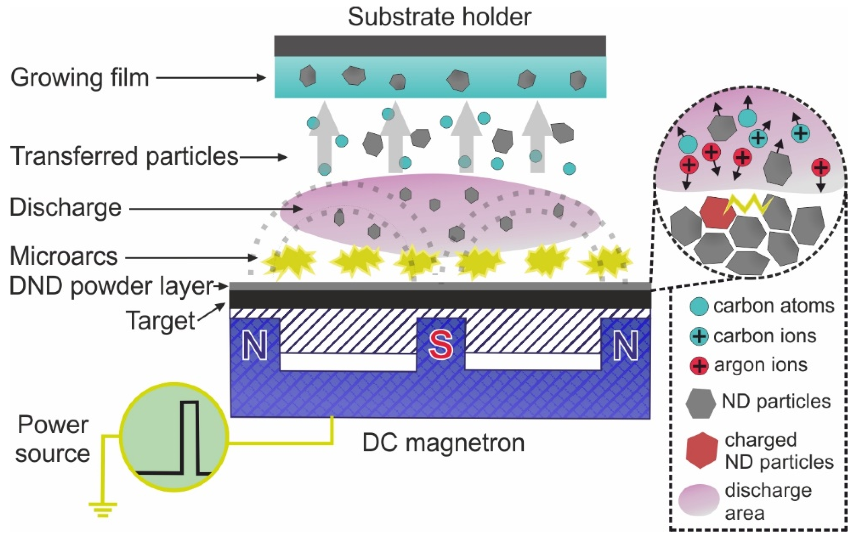
2.1. Target Manufacturing
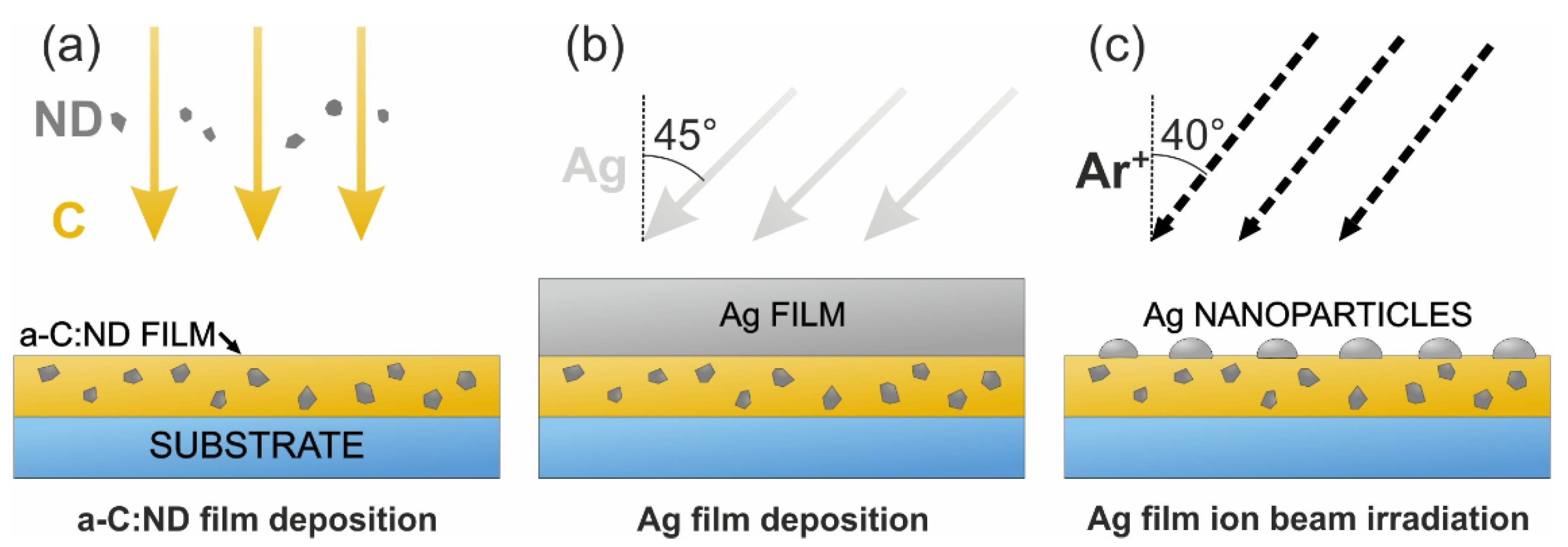
2.2. Deposition Stages
2.3. SERS-Active Media Formation
2.4. Structural Investigations
2.5. Estimation of DND Antimicrobial and Antifungal Activity
3. Results and Discussion
3.1. Characterization of a-C:ND Coating
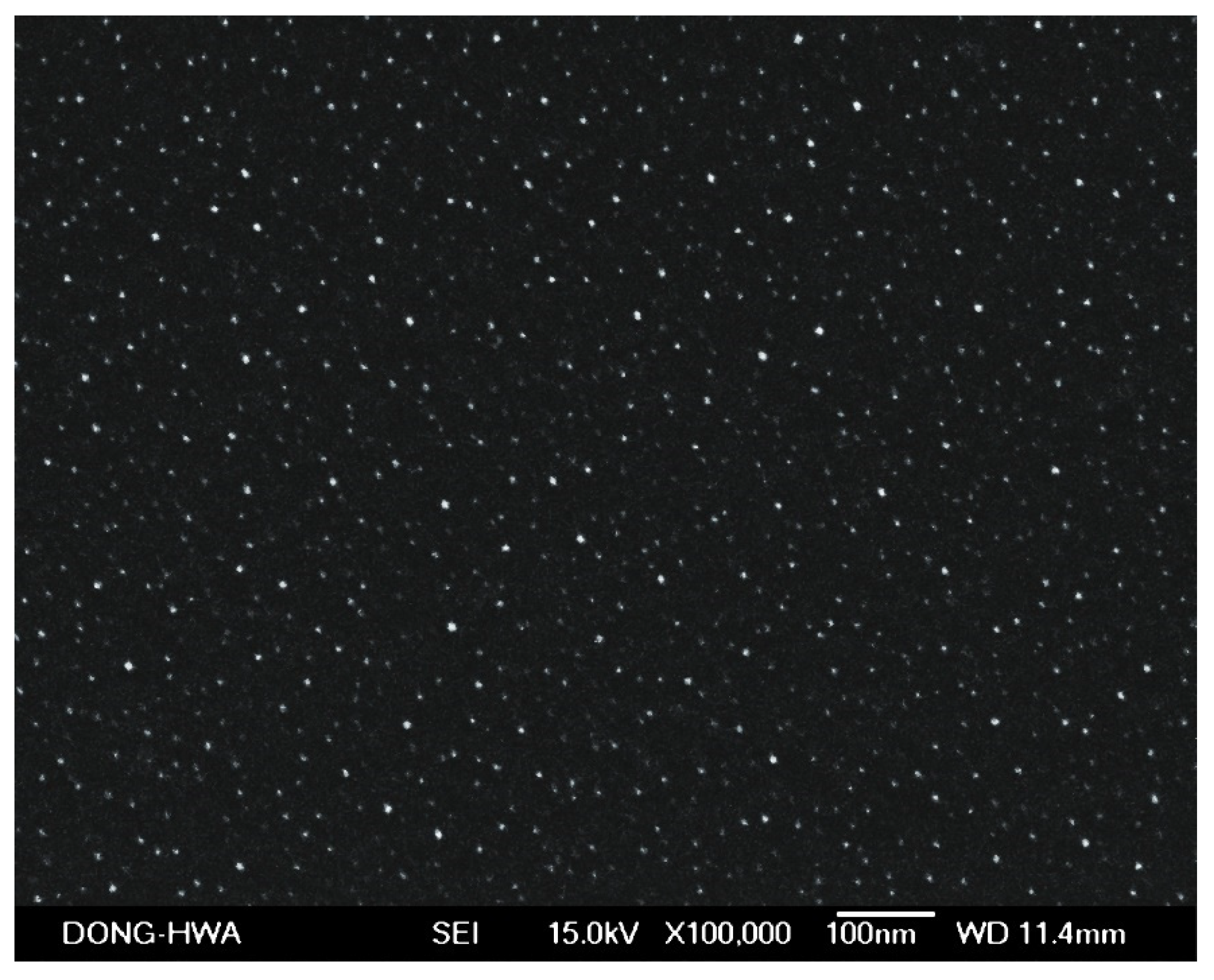
3.1.1. SEM
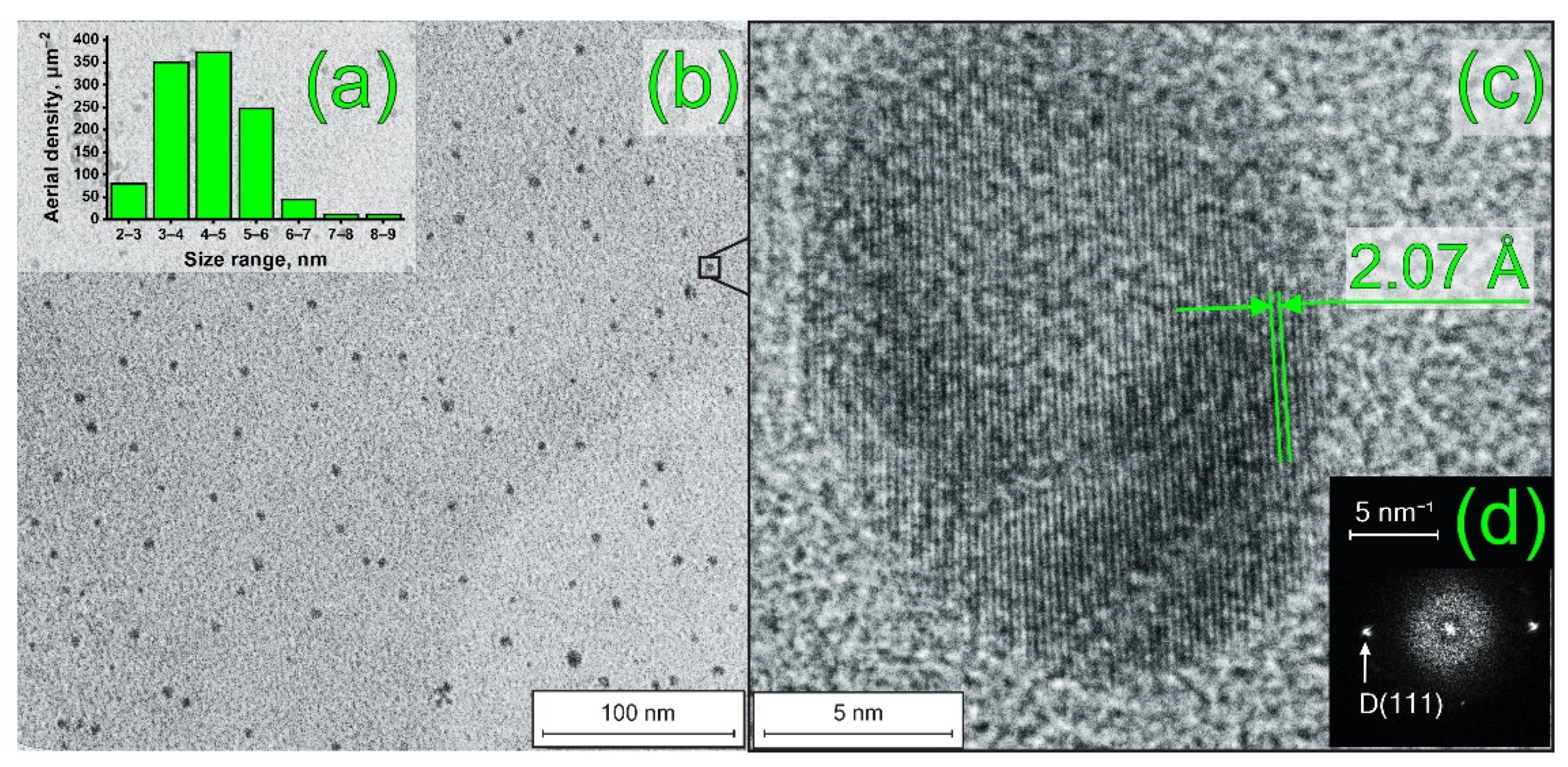
3.1.2. HRTEM
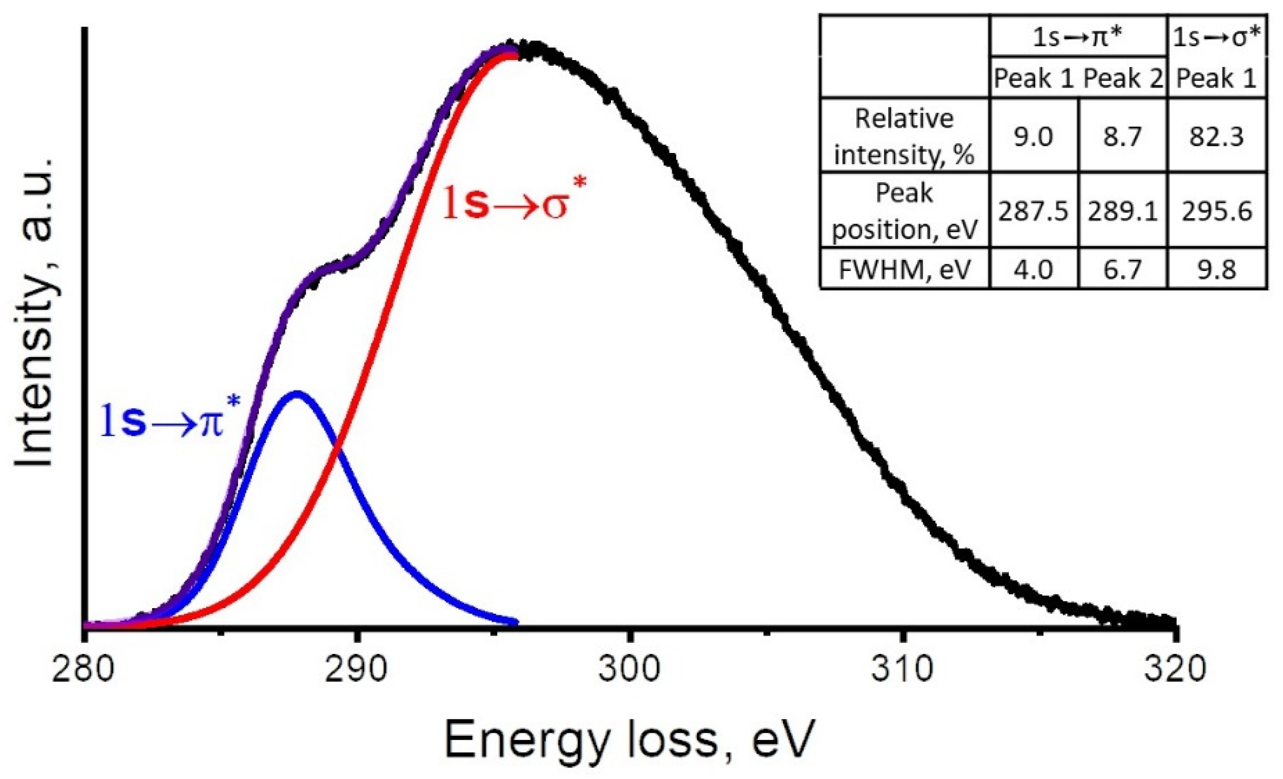
3.1.3. EELS
3.2. Ag Nanoparticles Characterization
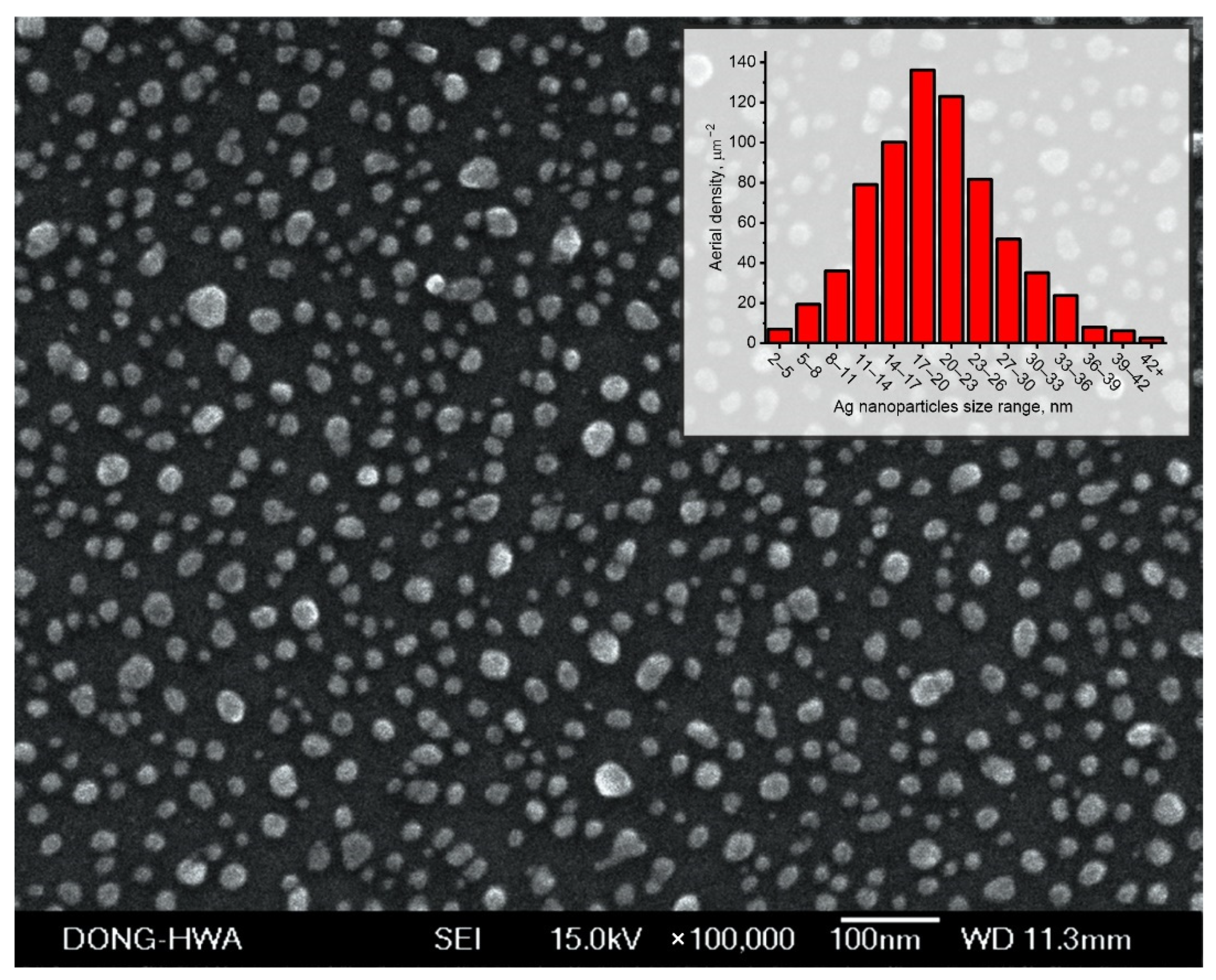
3.2.1. SEM
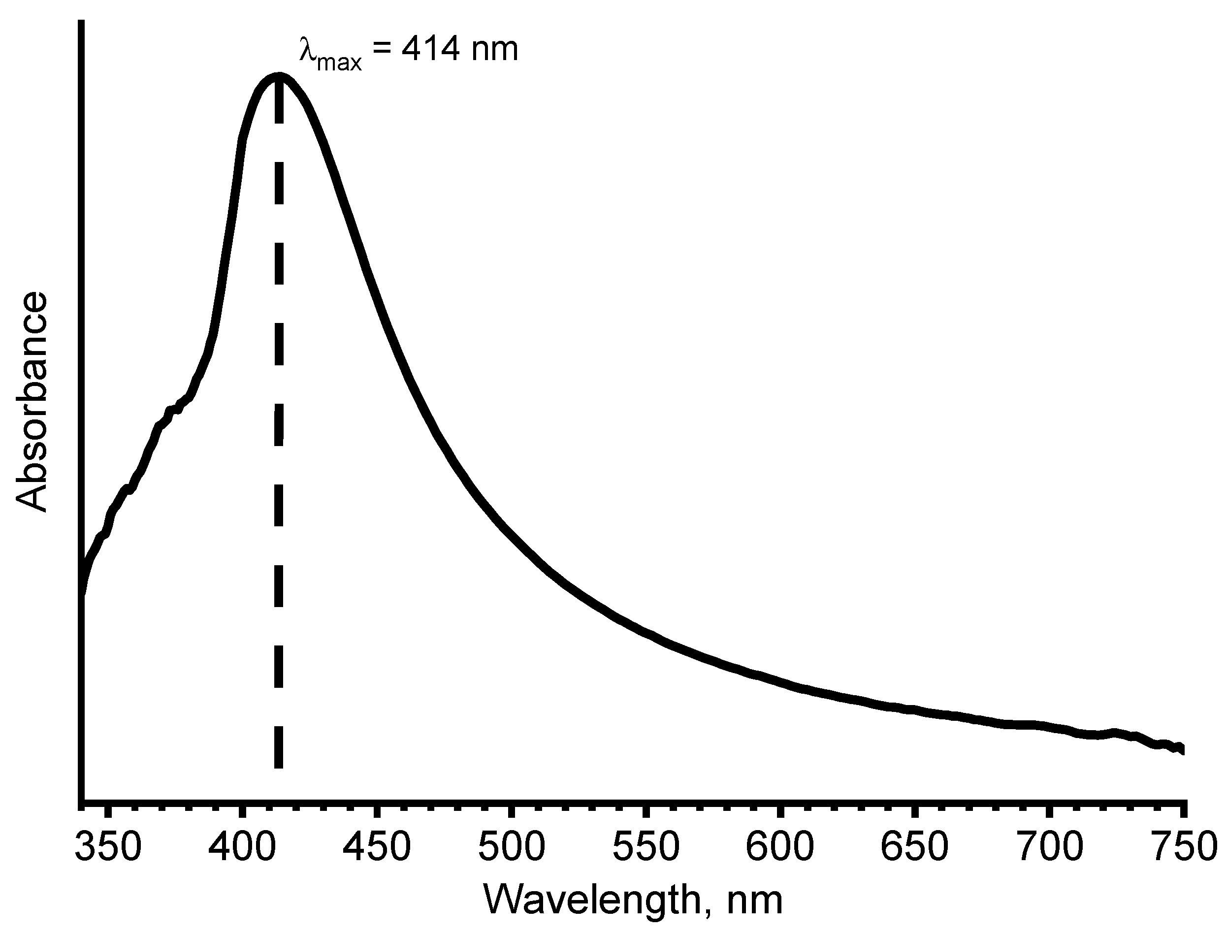
3.2.2. UV–Vis Absorbance Spectra
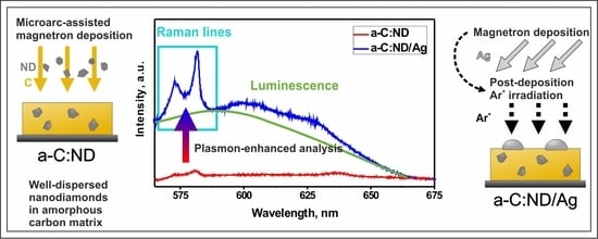
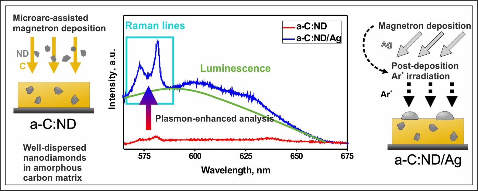
3.3. Raman Spectroscopy
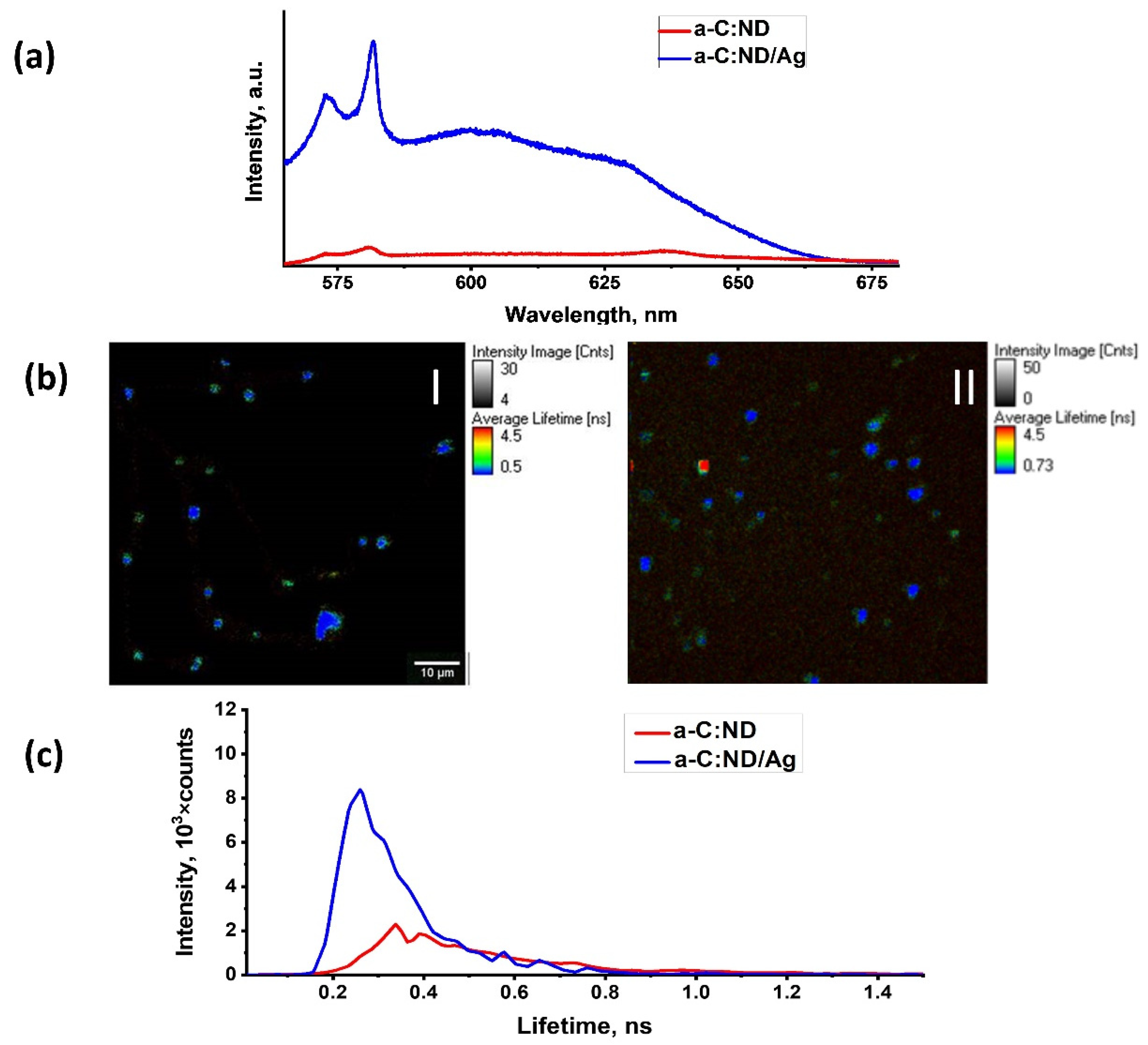
3.4. Photoluminescence of a-C:ND and a-C:ND/Ag
3.5. Assessment of the DND Antibacterial and Antifungal Effect
4. Key Findings
- (1)
- Microarc-assisted magnetron sputtering of the DND powder in pulsed mode was applied to manufacture the coating of NDs encapsulated in an amorphous carbon matrix, i.e., a-C:ND structure. EELS showed that the cumulative sp3/(sp2 + sp3) ratio of a-C:ND was 76%.
- (2)
- SEM and TEM revealed spatial uniformity of the distribution of encapsulated NDs and an absence of the NDs’ aggregation, thus resulting in good dispersion of the NDs in the a-C:ND structures.
- (3)
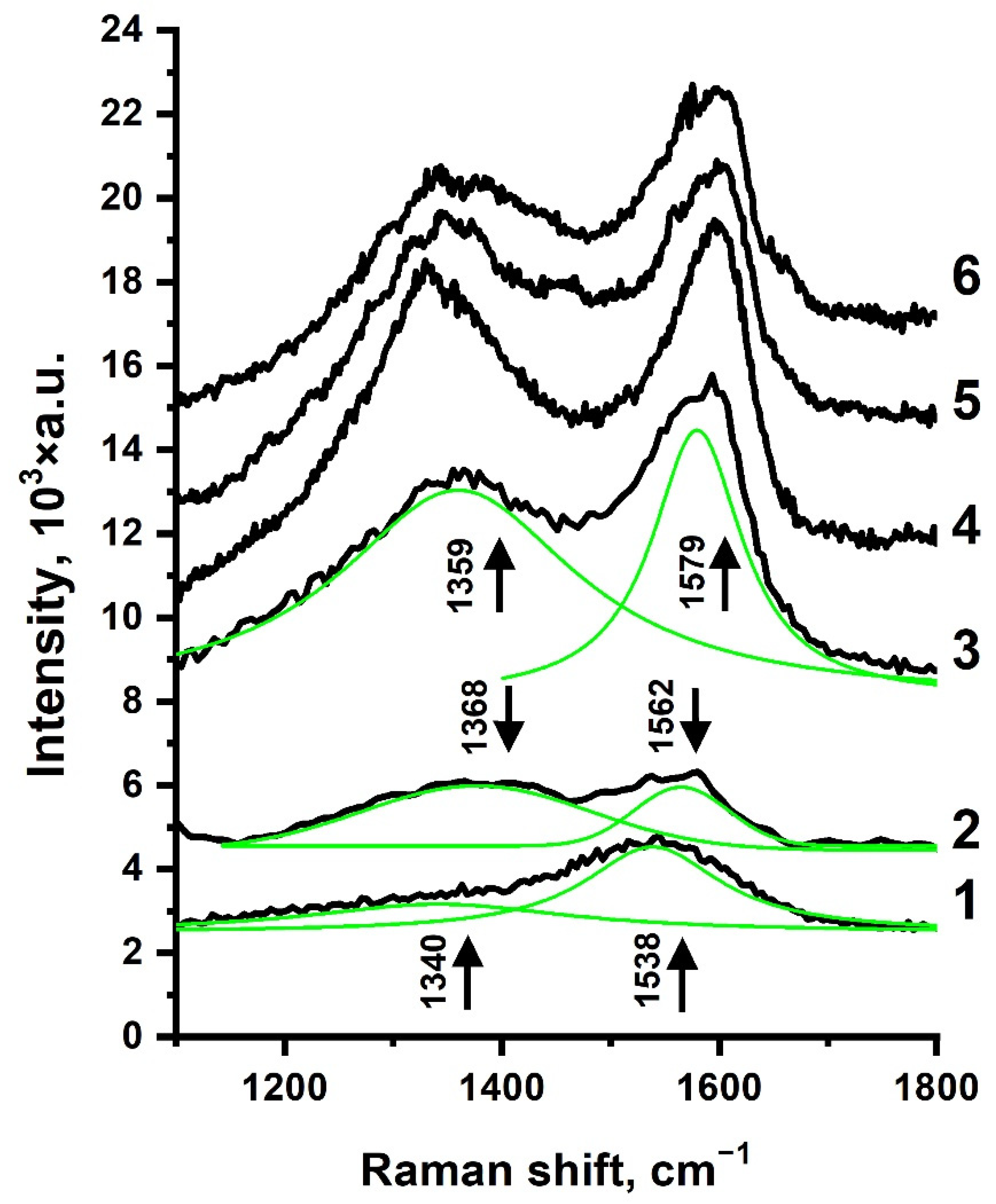
- The plasmonic properties of AgNP formed by low-energy Ar+ irradiation of continuous Ag film allowed us to observe the SERS effect on an a-C:ND/Ag structure. Spectra intensity enhancement only occurred several times, and a selective SERS sensitivity to nondiamond sp2-features was observed.
- (4)
- SERS studies indicated that ion irradiation of the Ag overlayer had only slightly changed the D and G lines of an a-C:ND film, proving that the suggested technique of the plasmonic-active structure formation had not altered the analyzed structure.
- (5)
- Two-photon-excited luminescence was observed from the ND particles both in a-C:ND and a-C:ND/Ag at near-infrared excitation with fs laser. The luminescence lifetime in both cases was ~< 0.1 ns. While the lifetime did not change as a result of the plasmon-enhanced study, increased Ag-modified TPL intensity was observed for a-C:ND/Ag in comparison with a-C:ND.
- (6)
- The agar diffusion method revealed the prominent inhibition effect of DNDs against the bacterial strains of B. subtilis, S. aureus, E. coli as well as against all of the test fungi strains (A. niger, C. albicans, and A. fumigatu).
5. Conclusions and Outlook
Author Contributions
Funding
Institutional Review Board Statement
Informed Consent Statement
Data Availability Statement
Conflicts of Interest
References
- Li, C.-C.; Huang, C.-L. Preparation of Clear Colloidal Solutions of Detonation Nanodiamond in Organic Solvents. Colloids Surf. A Physicochem. Eng. Asp. 2010, 353, 52–56. [Google Scholar] [CrossRef]
- Kulakova, I.I. Surface Chemistry of Nanodiamonds. Phys. Solid State 2004, 46, 636–643. [Google Scholar] [CrossRef]
- Vejpravová, J. Mixed Sp2–Sp3 Nanocarbon Materials: A Status Quo Review. Nanomaterials 2021, 11, 2469. [Google Scholar] [CrossRef]
- Shvidchenko, A.V.; Eidelman, E.D.; Vul’, A.Y.; Kuznetsov, N.M.; Stolyarova, D.Y.; Belousov, S.I.; Chvalun, S.N. Colloids of Detonation Nanodiamond Particles for Advanced Applications. Adv. Colloid Interface Sci. 2019, 268, 64–81. [Google Scholar] [CrossRef]
- Sivtsov, E.V.; Kalinin, A.V.; Gostev, A.I.; Smirnov, A.V.; Agibalova, L.V.; Shumilov, F.A. In Situ Preparation of Polymer Nanocomposites Based on Sols of Surface-Modified Detonation Nanodiamonds by Classical and Controlled Radical Polymerization. Polym. Sci. Ser. B 2020, 62, 734–749. [Google Scholar] [CrossRef]
- Streletskiy, O.A.; Zavidovskiy, I.A.; Sychev, V.V.; Dudin, A.A.; Savinov, S.A.; Pavlikov, A.V. Magnetron Deposition of A-C:ND Coatings by Nanodiamond Transfer: Pulse Number Impact on Aggregation and Graphitization. Appl. Phys. A 2022, 128, 83. [Google Scholar] [CrossRef]
- Lenzini, F.; Gruhler, N.; Walter, N.; Pernice, W.H.P. Diamond as a Platform for Integrated Quantum Photonics. Adv. Quantum Technol. 2018, 1, 1800061. [Google Scholar] [CrossRef]
- Chen, Y.G.; Ogura, M.; Okushi, H. Schottky Junction Properties on High Quality Boron-Doped Homoepitaxial Diamond Thin Films. J. Vac. Sci. Technol. B Microelectron. Nanometer Struct. Processing Meas. Phenom. 2004, 22, 2084–2086. [Google Scholar] [CrossRef]
- Basso, L.; Cazzanelli, M.; Orlandi, M.; Miotello, A. Nanodiamonds: Synthesis and Application in Sensing, Catalysis, and the Possible Connection with Some Processes Occurring in Space. Appl. Sci. 2020, 10, 4094. [Google Scholar] [CrossRef]
- Petráková, V.; Taylor, A.; Kratochvílová, I.; Fendrych, F.; Vacík, J.; Kučka, J.; Štursa, J.; Cígler, P.; Ledvina, M.; Fišerová, A.; et al. Luminescence of Nanodiamond Driven by Atomic Functionalization: Towards Novel Detection Principles. Adv. Funct. Mater. 2012, 22, 812–819. [Google Scholar] [CrossRef]
- Hui, Y.Y.; Chen, O.Y.; Azuma, T.; Chang, B.-M.; Hsieh, F.-J.; Chang, H.-C. All-Optical Thermometry with Nitrogen-Vacancy Centers in Nanodiamond-Embedded Polymer Films. J. Phys. Chem. C 2019, 123, 15366–15374. [Google Scholar] [CrossRef]
- Tallaire, A.; Brinza, O.; De Feudis, M.; Ferrier, A.; Touati, N.; Binet, L.; Nicolas, L.; Delord, T.; Hétet, G.; Herzig, T.; et al. Synthesis of Loose Nanodiamonds Containing Nitrogen-Vacancy Centers for Magnetic and Thermal Sensing. ACS Appl. Nano Mater. 2019, 2, 5952–5962. [Google Scholar] [CrossRef]
- Iyer, A.; Etula, J.; Ge, Y.; Liu, X.; Koskinen, J. Nanodiamond Embedded Ta-C Composite Film by Pulsed Filtered Vacuum Arc Deposition from a Single Target. Appl. Phys. Lett. 2016, 109, 201905. [Google Scholar] [CrossRef] [Green Version]
- Claveau, S.; Bertrand, J.-R.; Treussart, F. Fluorescent Nanodiamond Applications for Cellular Process Sensing and Cell Tracking. Micromachines 2018, 9, 247. [Google Scholar] [CrossRef] [PubMed] [Green Version]
- Lin, Y.-C.; Tsai, L.-W.; Perevedentseva, E.; Karmenyan, A.; Cheng, C.-L. Near-Infrared Fluorescence from Nanodiamond for Multimodal Bioimaging. Sovrem. Tehnol. V Med. 2018, 10, 49–56. [Google Scholar] [CrossRef] [Green Version]
- Tisler, J.; Reuter, R.; Lämmle, A.; Jelezko, F.; Balasubramanian, G.; Hemmer, P.R.; Reinhard, F.; Wrachtrup, J. Highly Efficient FRET from a Single Nitrogen-Vacancy Center in Nanodiamonds to a Single Organic Molecule. ACS Nano 2011, 5, 7893–7898. [Google Scholar] [CrossRef] [Green Version]
- Börsch, M.; Reuter, R.; Balasubramanian, G.; Erdmann, R.; Jelezko, F.; Wrachtrup, J. Fluorescent Nanodiamonds for FRET-Based Monitoring of a Single Biological Nanomotor FoF1-ATP Synthase. In Proceedings of the Multiphoton Microscopy in the Biomedical Sciences IX, SPIE, San Jose, CA, USA, 13 February 2009; Volume 7183, pp. 496–505. [Google Scholar]
- Wang, Y.; Wang, L.; Wang, S.C.; Zhang, G.; Wood, R.J.K.; Xue, Q. Nanocomposite Microstructure and Environment Self-Adapted Tribological Properties of Highly Hard Graphite-Like Film. Tribol. Lett. 2010, 40, 301–310. [Google Scholar] [CrossRef]
- Naragino, H.; Egiza, M.; Tominaga, A.; Murasawa, K.; Gonda, H.; Sakurai, M.; Yoshitake, T. Hard Coating of Ultrananocrystalline Diamond/Nonhydrogenated Amorphous Carbon Composite Films on Cemented Tungsten Carbide by Coaxial Arc Plasma Deposition. Appl. Phys. A 2016, 122, 761. [Google Scholar] [CrossRef]
- Ali, A.M.; Deckert-Gaudig, T.; Egiza, M.; Deckert, V.; Yoshitake, T. Near- and Far-Field Raman Spectroscopic Studies of Nanodiamond Composite Films Deposited by Coaxial Arc Plasma. Appl. Phys. Lett. 2020, 116, 041601. [Google Scholar] [CrossRef]
- Ali, A.M.; Egiza, M.; Murasawa, K.; Sugita, H.; Deckert-Gaudig, T.; Deckert, V.; Yoshitake, T. Effects of Substrate Temperature and Intermediate Layer on Adhesion, Structural and Mechanical Properties of Coaxial Arc Plasma Deposition Grown Nanodiamond Composite Films on Si Substrates. Surf. Coat. Technol. 2021, 417, 127185. [Google Scholar] [CrossRef]
- Takeichi, S.; Nishiyama, T.; Tabara, M.; Kawawaki, S.; Kohno, M.; Takahashi, K.; Yoshitake, T. Thermal Conductivity of Ultrananocrystalline Diamond/Hydrogenated Amorphous Carbon Composite Films Prepared by Coaxial Arc Plasma Deposition. ECS Trans. 2017, 75, 27. [Google Scholar] [CrossRef]
- Shaban, M. Determination of Trap Density-of-States Distribution of Nitrogen-Doped Ultrananocrystalline Diamond/Hydrogenated Amorphous Carbon Composite Films. J. Semicond. 2021, 42, 062802–062807. [Google Scholar] [CrossRef]
- Nistor, P.A.; May, P.W. Diamond Thin Films: Giving Biomedical Applications a New Shine. J. R. Soc. Interface 2017, 14, 20170382. [Google Scholar] [CrossRef] [PubMed] [Green Version]
- Islam, M.; Lantada, A.D.; Mager, D.; Korvink, J.G. Carbon-Based Materials for Articular Tissue Engineering: From Innovative Scaffolding Materials toward Engineered Living Carbon. Adv. Healthc. Mater. 2022, 11, 2101834. [Google Scholar] [CrossRef] [PubMed]
- Carvalho, I.; Rodrigues, L.; Lima, M.J.; Carvalho, S.; Cruz, S.M.A. Overview on the Antimicrobial Activity and Biocompatibility of Sputtered Carbon-Based Coatings. Processes 2021, 9, 1428. [Google Scholar] [CrossRef]
- Kaneko, M.; Hiratsuka, M.; Alanazi, A.; Nakamori, H.; Namiki, K.; Hirakuri, K. Surface Reformation of Medical Devices with DLC Coating. Materials 2021, 14, 376. [Google Scholar] [CrossRef]
- Novikov, S.M.; Streletskiy, O.A.; Doroshina, N.V.; Yakubovsky, D.I.; Mironov, M.S.; Sychev, V.V.; Voronov, A.A.; Arsenin, A.V.; Volkov, V.S. Long-Term Stable Structures Formed by Ion-Beam Modification of Silver Film for SERS Applications. J. Phys. Conf. Ser. 2021, 2015, 012099. [Google Scholar] [CrossRef]
- Streletskiy, O.; Zavidovskiy, I.; Yakubovsky, D.; Doroshina, N.; Syuy, A.; Lebedinskij, Y.; Markeev, A.; Arsenin, A.; Volkov, V.; Novikov, S. Tailoring of the Distribution of SERS-Active Silver Nanoparticles by Post-Deposition Low-Energy Ion Beam Irradiation. Materials 2022, 15, 7721. [Google Scholar] [CrossRef]
- Veres, M.; Füle, M.; Tóth, S.; Koós, M.; Pócsik, I. Surface Enhanced Raman Scattering (SERS) Investigation of Amorphous Carbon. Diam. Relat. Mater. 2004, 13, 1412–1415. [Google Scholar] [CrossRef]
- Nascimento, G.M.D. Raman Spectroscopy; IntechOpen: London, UK, 2018; ISBN 978-1-78923-000-0. [Google Scholar] [CrossRef]
- Karmenyan, A.V.; Perevedentseva, E.; Veres, M.; Cheng, C.-L. Simultaneous Photoluminescence and SERS Observation of Nanodiamond at Laser Deposition on Noble Metals. Plasmonics 2013, 8, 325–333. [Google Scholar] [CrossRef]
- European Committee on Antimicrobial Susceptibility Testing Antimicrobial Susceptibility Testing. EUCAST Disk Diffusion Method. Available online: https://www.eucast.org/fileadmin/src/media/PDFs/EUCAST_files/Disk_test_documents/2021_manuals/Manual_v_9.0_EUCAST_Disk_Test_2021.pdf (accessed on 31 October 2022).
- Yang, B.; Li, J.; Guo, L.; Huang, N.; Liu, L.; Zhai, Z.; Long, W.; Jiang, X. Fabrication of Silicon-Vacancy Color Centers in Diamond Films: Tetramethylsilane as a New Dopant Source. CrystEngComm 2018, 20, 1158–1167. [Google Scholar] [CrossRef]
- Noborisaka, M.; Horikoshi, R.; Nagashima, S.; Shirakura, A.; Suzuki, T. Hardness and Surface Roughness of Hydrogenated Amorphous Carbon-Based Films Synthesized by Atmospheric Pressure-Plasma Enhanced Chemical Vapor Deposition at Low Temperature. Thin Solid Film. 2013, 527, 114–119. [Google Scholar] [CrossRef]
- Simonot, L.; Chabanais, F.; Rousselet, S.; Pailloux, F.; Camelio, S.; Babonneau, D. Evolution of Plasmonic Nanostructures under Ultra-Low-Energy Ion Bombardment. Appl. Surf. Sci. 2021, 544, 148672. [Google Scholar] [CrossRef]
- Klimmer, A.; Ziemann, P.; Biskupek, J.; Kaiser, U.; Flesch, M. Size-Dependent Effect of Ion Bombardment on Au Nanoparticles on Top of Various Substrates: Thermodynamically Dominated Capillary Forces versus Sputtering. Phys. Rev. B 2009, 79, 155427. [Google Scholar] [CrossRef]
- Murty, M.V.R. Sputtering: The Material Erosion Tool. Surf. Sci. 2002, 500, 523–544. [Google Scholar] [CrossRef]
- Resta, V.; Peláez, R.J.; Afonso, C.N. Importance of Ion Bombardment during Coverage of Au Nanoparticles on Their Structural Features and Optical Response. J. Appl. Phys. 2014, 115, 124303. [Google Scholar] [CrossRef] [Green Version]
- Nest, D.; Graves, D.B.; Engelmann, S.; Bruce, R.L.; Weilnboeck, F.; Oehrlein, G.S.; Andes, C.; Hudson, E.A. Synergistic Effects of Vacuum Ultraviolet Radiation, Ion Bombardment, and Heating in 193nm Photoresist Roughening and Degradation. Appl. Phys. Lett. 2008, 92, 153113. [Google Scholar] [CrossRef]
- Soltys, L.; Olkhovyy, O.; Tatarchuk, T.; Naushad, M. Green Synthesis of Metal and Metal Oxide Nanoparticles: Principles of Green Chemistry and Raw Materials. Magnetochemistry 2021, 7, 145. [Google Scholar] [CrossRef]
- Dobrev, D. Ion-Beam-Induced Texture Formation in Vacuum-Condensed Thin Metal Films. Thin Solid Film. 1982, 92, 41–53. [Google Scholar] [CrossRef]
- Novikov, S.M.; Popok, V.N.; Evlyukhin, A.B.; Hanif, M.; Morgen, P.; Fiutowski, J.; Beermann, J.; Rubahn, H.-G.; Bozhevolnyi, S.I. Highly Stable Monocrystalline Silver Clusters for Plasmonic Applications. Langmuir 2017, 33, 6062–6070. [Google Scholar] [CrossRef]
- Starowicz, Z.; Wojnarowska-Nowak, R.; Ozga, P.; Sheregii, E.M. The Tuning of the Plasmon Resonance of the Metal Nanoparticles in Terms of the SERS Effect. Colloid. Polym. Sci. 2018, 296, 1029–1037. [Google Scholar] [CrossRef] [PubMed] [Green Version]
- Jensen, T.; Kelly, L.; Lazarides, A.; Schatz, G.C. Electrodynamics of Noble Metal Nanoparticles and Nanoparticle Clusters. J. Clust. Sci. 1999, 10, 295–317. [Google Scholar] [CrossRef]
- Shanthil, M.; Thomas, R.; Swathi, R.S.; George Thomas, K. Ag@SiO2 Core–Shell Nanostructures: Distance-Dependent Plasmon Coupling and SERS Investigation. J. Phys. Chem. Lett. 2012, 3, 1459–1464. [Google Scholar] [CrossRef]
- Cortijo-Campos, S.; Ramírez-Jiménez, R.; Climent-Pascual, E.; Aguilar-Pujol, M.; Jiménez-Villacorta, F.; Martínez, L.; Jiménez-Riobóo, R.; Prieto, C.; de Andrés, A. Raman Amplification in the Ultra-Small Limit of Ag Nanoparticles on SiO2 and Graphene: Size and Inter-Particle Distance Effects. Mater. Des. 2020, 192, 108702. [Google Scholar] [CrossRef] [PubMed]
- Prawer, S.; Nemanich, R.J. Raman Spectroscopy of Diamond and Doped Diamond. Philos. Trans. R. Soc. London. Ser. A Math. Phys. Eng. Sci. 2004, 362, 2537–2565. [Google Scholar] [CrossRef]
- Dychalska, A.; Popielarski, P.; Franków, W.; Fabisiak, K.; Paprocki, K.; Szybowicz, M. Study of CVD Diamond Layers with Amorphous Carbon Admixture by Raman Scattering Spectroscopy. Mater. Sci. 2015, 33, 799–805. [Google Scholar] [CrossRef] [Green Version]
- Knight, D.S.; Weimer, R.; Pilione, L.; White, W.B. Surface-enhanced Raman Spectroscopy of Chemical Vapor Deposited Diamond Films. Appl. Phys. Lett. 1990, 56, 1320–1322. [Google Scholar] [CrossRef]
- Demirel, G.; Usta, H.; Yilmaz, M.; Celik, M.; Alidagi, H.A.; Buyukserin, F. Surface-Enhanced Raman Spectroscopy (SERS): An Adventure from Plasmonic Metals to Organic Semiconductors as SERS Platforms. J. Mater. Chem. C 2018, 6, 5314–5335. [Google Scholar] [CrossRef]
- Ferrari, A.C.; Robertson, J. Interpretation of Raman Spectra of Disordered and Amorphous Carbon. Phys. Rev. B 2000, 61, 14095–14107. [Google Scholar] [CrossRef]
- Ferrari, A.C.; Robertson, J. Origin of the 1150 Cm-1 Raman Mode in Nanocrystalline Diamond. Phys. Rev. B 2001, 63, 121405. [Google Scholar] [CrossRef]
- Zhang, D.; Zhang, R.Q. Signature of Nanodiamond in Raman Spectra: A Density Functional Theoretical Study. J. Phys. Chem. B 2005, 109, 9006–9013. [Google Scholar] [CrossRef] [PubMed]
- Zavidovskiy, I.A.; Streletskiy, O.A.; Nishchak, O.Y.; Haidarov, A.A.; Pavlikov, A.V. The Influence of Ion Assistance Energy on Structural and Optical Properties of Carbon-Silver Nanocomposites. Thin Solid Film. 2021, 738, 138966. [Google Scholar] [CrossRef]
- Kasuya, A.; Sasaki, Y.; Saito, Y.; Tohji, K.; Nishina, Y. Evidence for Size-Dependent Discrete Dispersions in Single-Wall Nanotubes. Phys. Rev. Lett. 1997, 78, 4434–4437. [Google Scholar] [CrossRef] [Green Version]
- Mews, A.; Koberling, F.; Basché, T.; Philipp, G.; Duesberg, G.; Roth, S.; Burghard, M. Raman Imaging of Single Carbon Nanotubes. Adv. Mater. 2000, 12, 1210–1214. [Google Scholar] [CrossRef]
- Claramunt, S.; Varea, A.; López-Díaz, D.; Velázquez, M.M.; Cornet, A.; Cirera, A. The Importance of Interbands on the Interpretation of the Raman Spectrum of Graphene Oxide. J. Phys. Chem. C 2015, 119, 10123–10129. [Google Scholar] [CrossRef]
- Caro, M.A.; Deringer, V.L.; Koskinen, J.; Laurila, T.; Csányi, G. Growth Mechanism and Origin of High Sp3 Content in Tetrahedral Amorphous Carbon. Phys. Rev. Lett. 2018, 120, 166101. [Google Scholar] [CrossRef] [Green Version]
- Wang, S.; Komvopoulos, K. A Molecular Dynamics Study of the Oxidation Mechanism, Nanostructure Evolution, and Friction Characteristics of Ultrathin Amorphous Carbon Films in Vacuum and Oxygen Atmosphere. Sci. Rep. 2021, 11, 3914. [Google Scholar] [CrossRef]
- Streletskiy, O.A.; Zavidovskiy, I.A.; Balabanyan, V.Y.; Tsiskarashvili, A.V. Antibacterial Properties of Modified A-C and Ta-C Coatings: The Effects of the Sp2/Sp3 Ratio, Oxidation, Nitridation, and Silver Incorporation. Appl. Phys. A 2022, 128, 929. [Google Scholar] [CrossRef]
- Vlasov, I.I.; Shenderova, O.A. Raman and Photoluminescence Spectroscopy of Detonation Nanodiamonds. In Detonation Nanodiamonds; Jenny Stanford Publishing: Stanford, CA, USA, 2013; ISBN 978-0-429-16896-3. [Google Scholar] [CrossRef]
- Aleksenskii, A.E.; Osipov, V.Y.; Vul’, A.Y.; Ber, B.Y.; Smirnov, A.B.; Melekhin, V.G.; Adriaenssens, G.J.; Iakoubovskii, K. Optical Properties of Nanodiamond Layers. Phys. Solid State 2001, 43, 145–150. [Google Scholar] [CrossRef]
- Hu, S.; Guo, Y.; Dong, Y.; Yang, J.; Liu, J.; Cao, S. Understanding the Effects of the Structures on the Energy Gaps in Carbon Nanoparticles from Laser Synthesis. J. Mater. Chem. 2012, 22, 12053–12057. [Google Scholar] [CrossRef]
- Reineck, P.; Lau, D.W.M.; Wilson, E.R.; Fox, K.; Field, M.R.; Deeleepojananan, C.; Mochalin, V.N.; Gibson, B.C. Effect of Surface Chemistry on the Fluorescence of Detonation Nanodiamonds. ACS Nano 2017, 11, 10924–10934. [Google Scholar] [CrossRef] [PubMed]
- Lim, T.-S.; Fu, C.-C.; Lee, K.-C.; Lee, H.-Y.; Chen, K.; Cheng, W.-F.; Wu, W.P.; Chang, H.-C.; Fann, W. Fluorescence Enhancement and Lifetime Modification of Single Nanodiamonds near a Nanocrystalline Silver Surface. Phys. Chem. Chem. Phys. 2009, 11, 1508–1514. [Google Scholar] [CrossRef] [PubMed]
- Song, J.; Li, H.; Lin, F.; Wang, L.; Wu, H.; Yang, Y. Plasmon-Enhanced Photoluminescence of Si-V Centers in Diamond from a Nanoassembled Metal–Diamond Hybrid Structure. CrystEngComm 2014, 16, 8356–8362. [Google Scholar] [CrossRef]
- Andersen, S.K.H.; Kumar, S.; Bozhevolnyi, S.I. Coupling of Nitrogen-Vacancy Centers in a Nanodiamond to a Silver Nanocube. Opt. Mater. Express OME 2016, 6, 3394–3406. [Google Scholar] [CrossRef]
- Gong, J.; Steinsultz, N.; Ouyang, M. Nanodiamond-Based Nanostructures for Coupling Nitrogen-Vacancy Centres to Metal Nanoparticles and Semiconductor Quantum Dots. Nat. Commun. 2016, 7, 11820. [Google Scholar] [CrossRef] [Green Version]
- Li, J.; Zhang, B.; Wang, F.; Liu, C. Silver/Carbon-Quantum-Dot Plasmonic Luminescent Nanoparticles. New J. Chem. 2011, 35, 554–557. [Google Scholar] [CrossRef]
- Bagra, B.; Zhang, W.; Zeng, Z.; Mabe, T.; Wei, J. Plasmon-Enhanced Fluorescence of Carbon Nanodots in Gold Nanoslit Cavities. Langmuir 2019, 35, 8903–8909. [Google Scholar] [CrossRef]
- Tóth, S.; Fule, M.; Veres, M.; Koós, M. Photoluminescence in Carbon-Based Amorphous Materials. In Optics and Electro-Optics Research; Nova Science Publishers, Inc.: New York, NY, USA, 2007; pp. 225–247. ISBN 978-1-60021-682-4. [Google Scholar]
- Fedotov, I.V.; Zheltikov, A.M. Background-Free Two-Photon Fluorescence Readout via a Three-Photon Charge-State Modulation of Nitrogen-Vacancy Centers in Diamond. Opt. Lett. 2019, 44, 3737–3740. [Google Scholar] [CrossRef]
- Johnstone, G.E.; Cairns, G.S.; Patton, B.R. Nanodiamonds Enable Adaptive-Optics Enhanced, Super-Resolution, Two-Photon Excitation Microscopy. R. Soc. Open Sci. 2019, 6, 190589. [Google Scholar] [CrossRef] [Green Version]
- Pan, L.; Sun, S.; Zhang, L.; Jiang, K.; Lin, H. Near-Infrared Emissive Carbon Dots for Two-Photon Fluorescence Bioimaging. Nanoscale 2016, 8, 17350–17356. [Google Scholar] [CrossRef]
- Lan, M.; Zhao, S.; Zhang, Z.; Yan, L.; Guo, L.; Niu, G.; Zhang, J.; Zhao, J.; Zhang, H.; Wang, P.; et al. Two-Photon-Excited near-Infrared Emissive Carbon Dots as Multifunctional Agents for Fluorescence Imaging and Photothermal Therapy. Nano Res. 2017, 10, 3113–3123. [Google Scholar] [CrossRef]
- Pramanik, A.; Fan, Z.; Chavva, S.R.; Sinha, S.S.; Ray, P.C. Highly Efficient and Excitation Tunable Two-Photon Luminescence Platform For Targeted Multi-Color MDRB Imaging Using Graphene Oxide. Sci. Rep. 2014, 4, 6090. [Google Scholar] [CrossRef] [PubMed] [Green Version]
- Perevedentseva, E.; Ali, N.; Karmenyan, A.; Skovorodkin, I.; Prunskaite-Hyyryläinen, R.; Vainio, S.; Cheng, C.-L.; Kinnunen, M. Optical Studies of Nanodiamond-Tissue Interaction: Skin Penetration and Localization. Materials 2019, 12, 3762. [Google Scholar] [CrossRef] [PubMed] [Green Version]
- Melentiev, P.N.; Afanasiev, A.E.; Kuzin, A.A.; Zablotskiy, A.V.; Balykin, V.I. Giant Enhancement of Two Photon Induced Luminescence in Metal Nanostructure. Opt. Express OE 2015, 23, 11444–11452. [Google Scholar] [CrossRef] [Green Version]
- Cumont, A.; Pitt, A.R.; Lambert, P.A.; Oggioni, M.R.; Ye, H. Properties, Mechanism and Applications of Diamond as an Antibacterial Material. Funct. Diam. 2021, 1, 1–28. [Google Scholar] [CrossRef]
- Chatterjee, A.; Perevedentseva, E.; Jani, M.; Cheng, C.-Y.; Ye, Y.-S.; Chung, P.-H.; Cheng, C.-L. Antibacterial Effect of Ultrafine Nanodiamond against Gram-Negative Bacteria Escherichia coli. J. Biomed. Opt. 2014, 20, 051014. [Google Scholar] [CrossRef]
- Szunerits, S.; Barras, A.; Boukherroub, R. Antibacterial Applications of Nanodiamonds. Int. J. Environ. Res. Public Health 2016, 13, 413. [Google Scholar] [CrossRef]
- Wang, C.; Makvandi, P.; Zare, E.N.; Tay, F.R.; Niu, L. Advances in Antimicrobial Organic and Inorganic Nanocompounds in Biomedicine. Adv. Ther. 2020, 3, 2000024. [Google Scholar] [CrossRef]
- Torres Sangiao, E.; Holban, A.M.; Gestal, M.C. Applications of Nanodiamonds in the Detection and Therapy of Infectious Diseases. Materials 2019, 12, 1639. [Google Scholar] [CrossRef] [Green Version]
- Fouda, S.M.; Gad, M.M.; Ellakany, P.; Al-Thobity, A.M.; Al-Harbi, F.A.; Virtanen, J.I.; Raustia, A. The Effect of Nanodiamonds on Candida albicans Adhesion and Surface Characteristics of PMMA Denture Base Material—An in Vitro Study. J. Appl. Oral Sci. 2019, 27, e20180779. [Google Scholar] [CrossRef] [Green Version]
- Pruskowski, K.A.; Mitchell, T.A.; Kiley, J.L.; Wellington, T.; Britton, G.W.; Cancio, L.C. Diagnosis and Management of Invasive Fungal Wound Infections in Burn Patients. Eur. Burn J. 2021, 2, 168–183. [Google Scholar] [CrossRef]
- Struck, M.F.; Gille, J. Fungal Infections in Burns: A Comprehensive Review. Ann. Burn. Fire Disasters 2013, 26, 147–153. [Google Scholar]
- Szunerits, S.; Boukherroub, R. Antibacterial Activity of Graphene-Based Materials. J. Mater. Chem. B 2016, 4, 6892–6912. [Google Scholar] [CrossRef] [Green Version]
- Jira, J.; Rezek, B.; Kriha, V.; Artemenko, A.; Matolínová, I.; Skakalova, V.; Stenclova, P.; Kromka, A. Inhibition of E. coli Growth by Nanodiamond and Graphene Oxide Enhanced by Luria-Bertani Medium. Nanomaterials 2018, 8, 140. [Google Scholar] [CrossRef] [PubMed] [Green Version]
- Nunes-Pereira, J.; Costa, P.; Fernandes, L.; Carvalho, E.O.; Fernandes, M.M.; Carabineiro, S.A.C.; Buijnsters, J.G.; Tubio, C.R.; Lanceros-Mendez, S. Antimicrobial and Antibiofilm Properties of Fluorinated Polymers with Embedded Functionalized Nanodiamonds. ACS Appl. Polym. Mater. 2020, 2, 5014–5024. [Google Scholar] [CrossRef]
- Kumar, P.; Huo, P.; Zhang, R.; Liu, B. Antibacterial Properties of Graphene-Based Nanomaterials. Nanomaterials 2019, 9, 737. [Google Scholar] [CrossRef] [Green Version]
- Hochvaldová, L.; Panáček, D.; Válková, L.; Prucek, R.; Kohlová, V.; Večeřová, R.; Kolář, M.; Kvítek, L.; Panáček, A. Restoration of Antibacterial Activity of Inactive Antibiotics via Combined Treatment with a Cyanographene/Ag Nanohybrid. Sci. Rep. 2022, 12, 5222. [Google Scholar] [CrossRef]
- Vi, T.T.T.; Kumar, S.R.; Pang, J.-H.S.; Liu, Y.-K.; Chen, D.W.; Lue, S.J. Synergistic Antibacterial Activity of Silver-Loaded Graphene Oxide towards Staphylococcus aureus and Escherichia coli. Nanomaterials 2020, 10, 366. [Google Scholar] [CrossRef] [Green Version]
- Wehling, J.; Dringen, R.; Zare, R.N.; Maas, M.; Rezwan, K. Bactericidal Activity of Partially Oxidized Nanodiamonds. ACS Nano 2014, 8, 6475–6483. [Google Scholar] [CrossRef]
- Turcheniuk, V.; Turcheniuk, K.; Bouckaert, J.; Barras, A.; Dumych, T.; Bilyy, R.; Zaitsev, V.; Siriwardena, A.; Wang, Q.; Boukherroub, R.; et al. Affinity of Glycan-Modified Nanodiamonds towards Lectins and Uropathogenic Escherichia coli. ChemNanoMat 2016, 2, 307–314. [Google Scholar] [CrossRef] [Green Version]
- Iyer, J.K.; Dickey, A.; Rouhani, P.; Kaul, A.; Govindaraju, N.; Singh, R.N.; Kaul, R. Nanodiamonds Facilitate Killing of Intracellular Uropathogenic E. coli in an in Vitro Model of Urinary Tract Infection Pathogenesis. PLoS ONE 2018, 13, e0191020. [Google Scholar] [CrossRef] [PubMed] [Green Version]
- Panáček, D.; Hochvaldová, L.; Bakandritsos, A.; Malina, T.; Langer, M.; Belza, J.; Martincová, J.; Večeřová, R.; Lazar, P.; Poláková, K.; et al. Silver Covalently Bound to Cyanographene Overcomes Bacterial Resistance to Silver Nanoparticles and Antibiotics. Adv. Sci. 2021, 8, 2003090. [Google Scholar] [CrossRef] [PubMed]
- Lin, Y.-C.; Perevedentseva, E.; Tsai, L.-W.; Wu, K.-T.; Cheng, C.-L. Nanodiamond for Intracellular Imaging in the Microorganisms in Vivo. J. Biophotonics 2012, 5, 838–847. [Google Scholar] [CrossRef] [PubMed]
- Gutiérrez, J.M.B.; Conceição, K.; de Andrade, V.M.; Trava-Airoldi, V.J.; Capote, G. High Antibacterial Properties of DLC Film Doped with Nanodiamond. Surf. Coat. Technol. 2019, 375, 395–401. [Google Scholar] [CrossRef]


| Spectrum | D-Peak | G-Peak | ID/IG | ||||
|---|---|---|---|---|---|---|---|
| Xc, cm−1 | W, cm−1 | A, 103 × a.u. | Xc, cm−1 | W, cm−1 | A, 103 × a.u. | ||
| 1 | 1340 ± 10 | 290 ± 28 | 294 ± 30 | 1538 ± 2 | 153 ± 6 | 481 ± 24 | 0.61 ± 0.09 |
| 2 | 1368 ± 3 | 271 ± 11 | 392.5 ± 9 | 1562 ± 1 | 102 ± 5 | 151 ± 5 | 2.59 ± 0.13 |
| 3 | 1359 ± 2 | 268 ± 9 | 1578 ± 50 | 1579 ± 1 | 101 ± 3 | 955 ± 34 | 1.65 ± 0.12 |
| B. subtilis ATCC 6633 | P. aeruginosa ATCC 27853 | M. luteus NCTC 8340 | S.aureus 209 | E. coli ATCC 25922 | A. niger INA 00760 | C. albicans ATCC 2091 | A. fumigatus KPB F-37 | |
|---|---|---|---|---|---|---|---|---|
| DND | 11 ± 0.2 | 0 | 0 | 9 ± 0.1 | 11 ± 0.1 | 11 ± 0.3 | 11 ± 0.2 | 11 ± 0.1 |
| amoxiclav | 18 ± 0.4 | 11 ± 0.2 | 24 ± 0.1 | 25 ± 0.3 | 11 ± 0.1 | nt * | nt * | nt * |
| amphotericin B | nt * | nt * | nt * | nt * | nt * | 17 ± 0.1 | 11 ± 0.09 | 10 ± 0.1 |
Publisher’s Note: MDPI stays neutral with regard to jurisdictional claims in published maps and institutional affiliations. |
© 2022 by the authors. Licensee MDPI, Basel, Switzerland. This article is an open access article distributed under the terms and conditions of the Creative Commons Attribution (CC BY) license (https://creativecommons.org/licenses/by/4.0/).
Share and Cite
Streletskiy, O.; Perevedentseva, E.; Zavidovskiy, I.; Karmenyan, A.; Sychev, V.; Sadykova, V.; Kuvarina, A.; Cheng, C.-L. Amorphous Carbon Films with Embedded Well-Dispersed Nanodiamonds: Plasmon-Enhanced Analysis and Possible Antimicrobial Applications. Magnetochemistry 2022, 8, 171. https://doi.org/10.3390/magnetochemistry8120171
Streletskiy O, Perevedentseva E, Zavidovskiy I, Karmenyan A, Sychev V, Sadykova V, Kuvarina A, Cheng C-L. Amorphous Carbon Films with Embedded Well-Dispersed Nanodiamonds: Plasmon-Enhanced Analysis and Possible Antimicrobial Applications. Magnetochemistry. 2022; 8(12):171. https://doi.org/10.3390/magnetochemistry8120171
Chicago/Turabian StyleStreletskiy, Oleg, Elena Perevedentseva, Ilya Zavidovskiy, Artashes Karmenyan, Vladimir Sychev, Vera Sadykova, Anastasia Kuvarina, and Chia-Liang Cheng. 2022. "Amorphous Carbon Films with Embedded Well-Dispersed Nanodiamonds: Plasmon-Enhanced Analysis and Possible Antimicrobial Applications" Magnetochemistry 8, no. 12: 171. https://doi.org/10.3390/magnetochemistry8120171