
Experimental Spectroscopic Data of SnO2 Films and Powder
 , , and
Abstract
:1. Summary
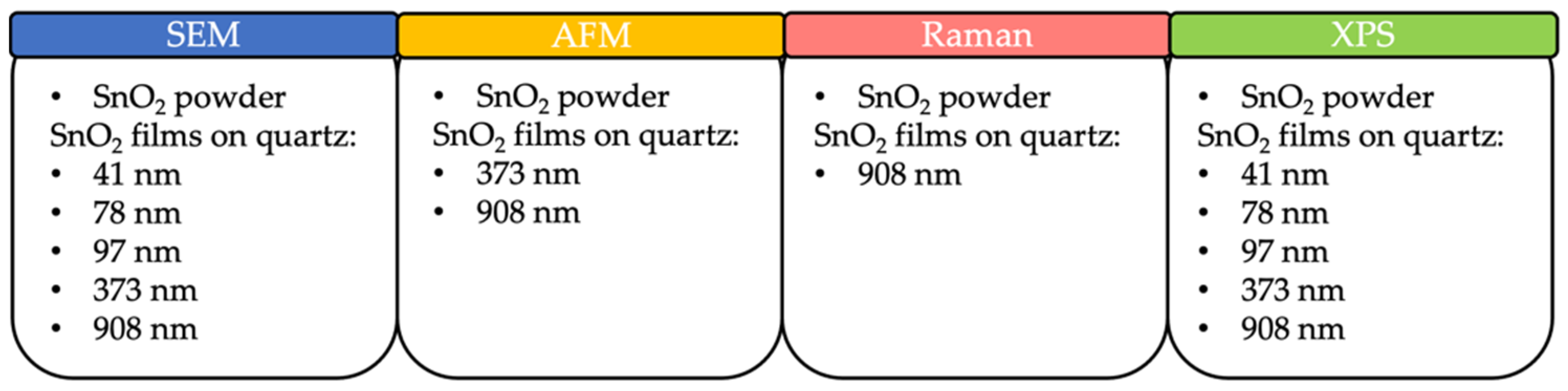
2. Data Description
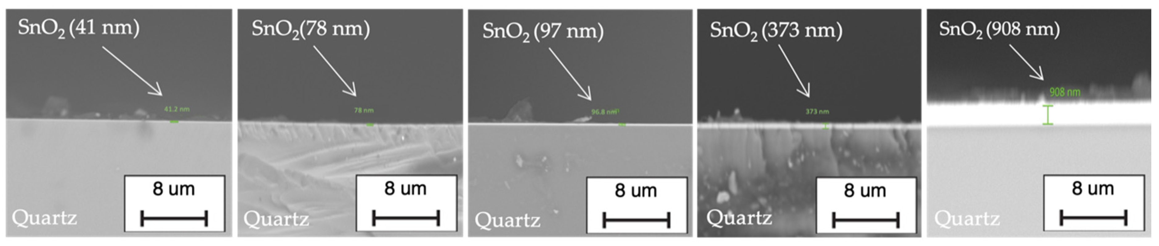
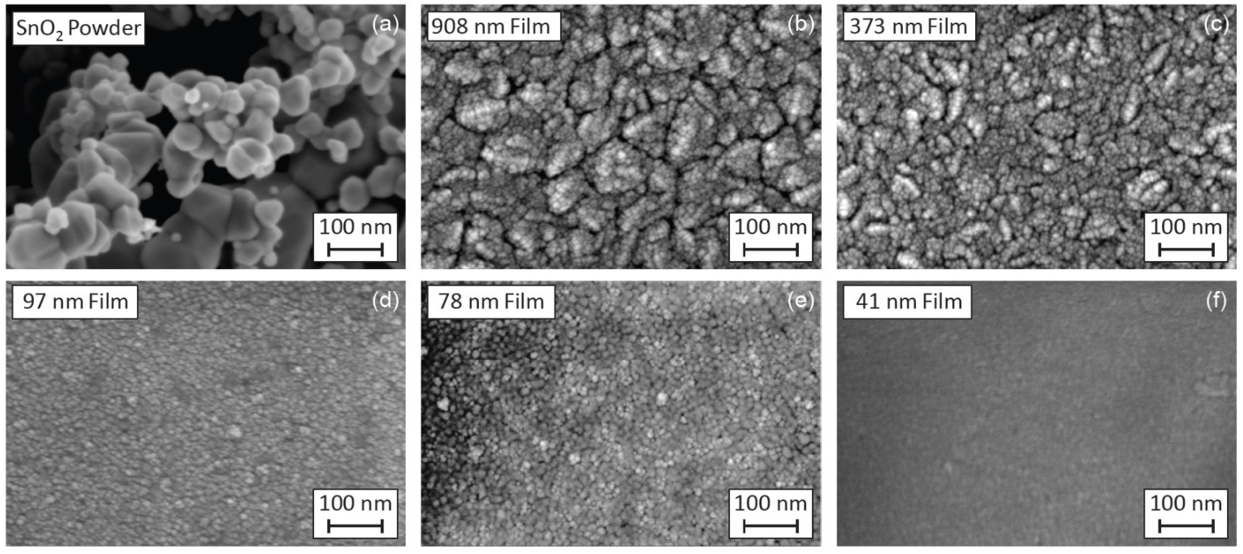
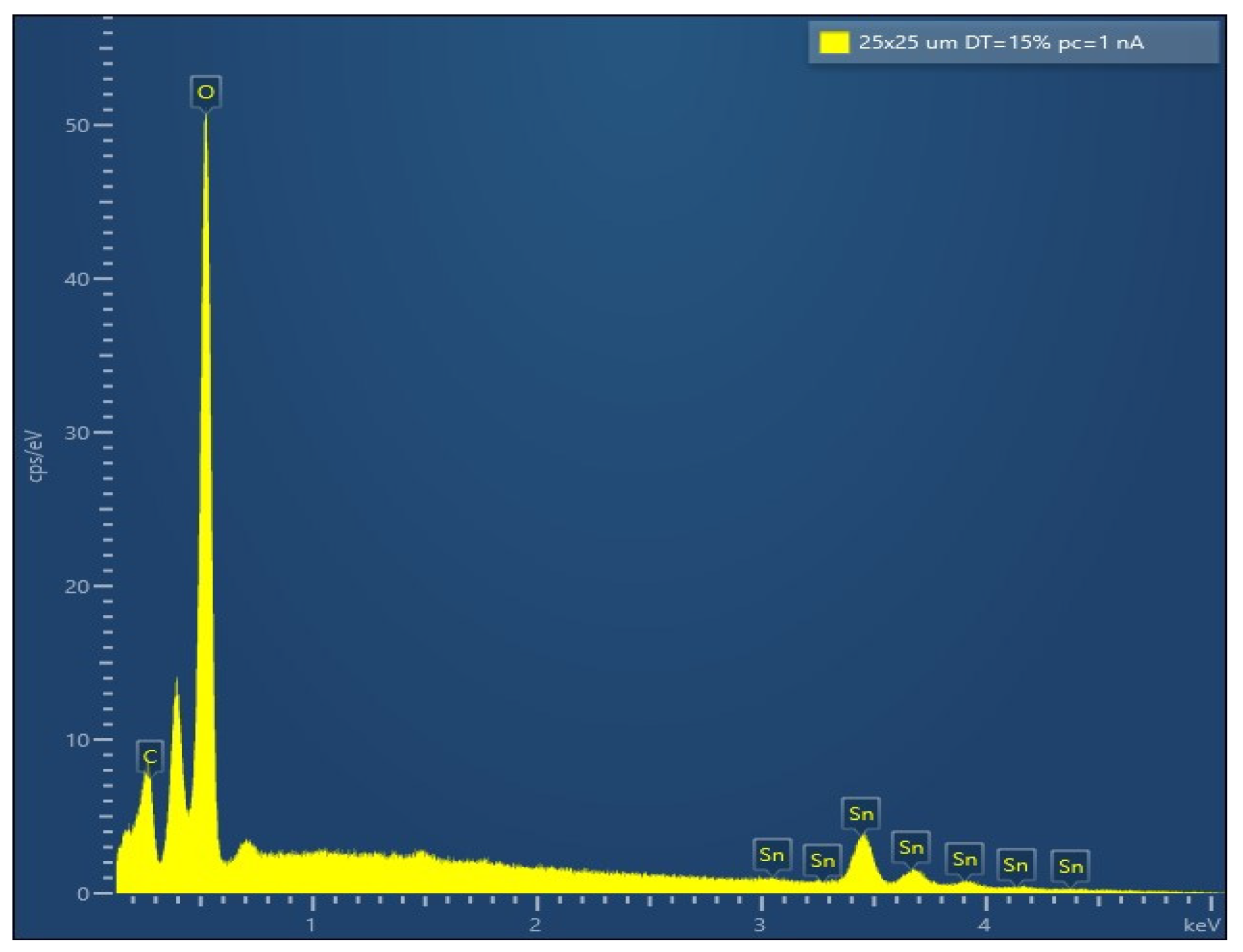
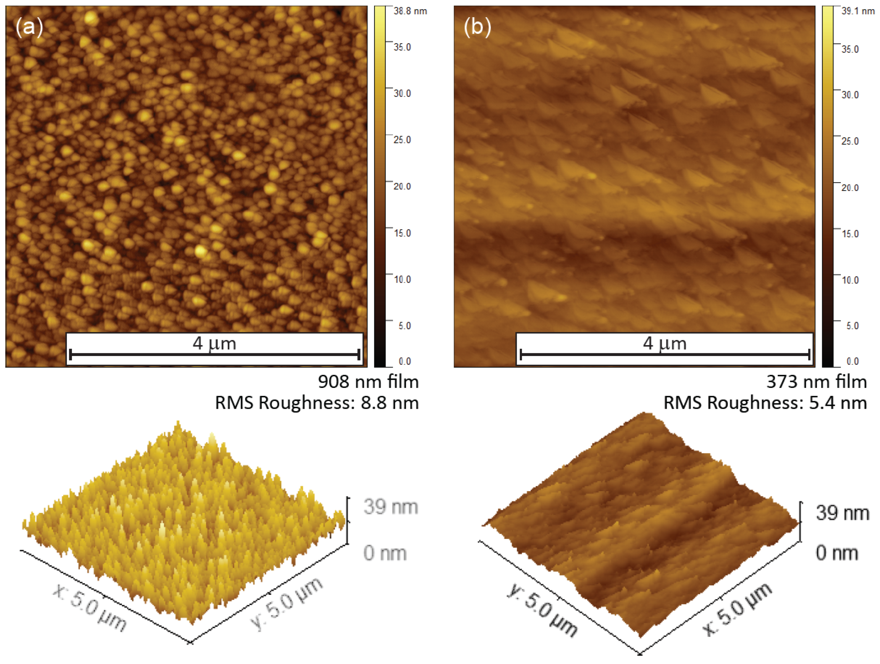
2.1. Scanning Electron and Atomic Force Microscopy
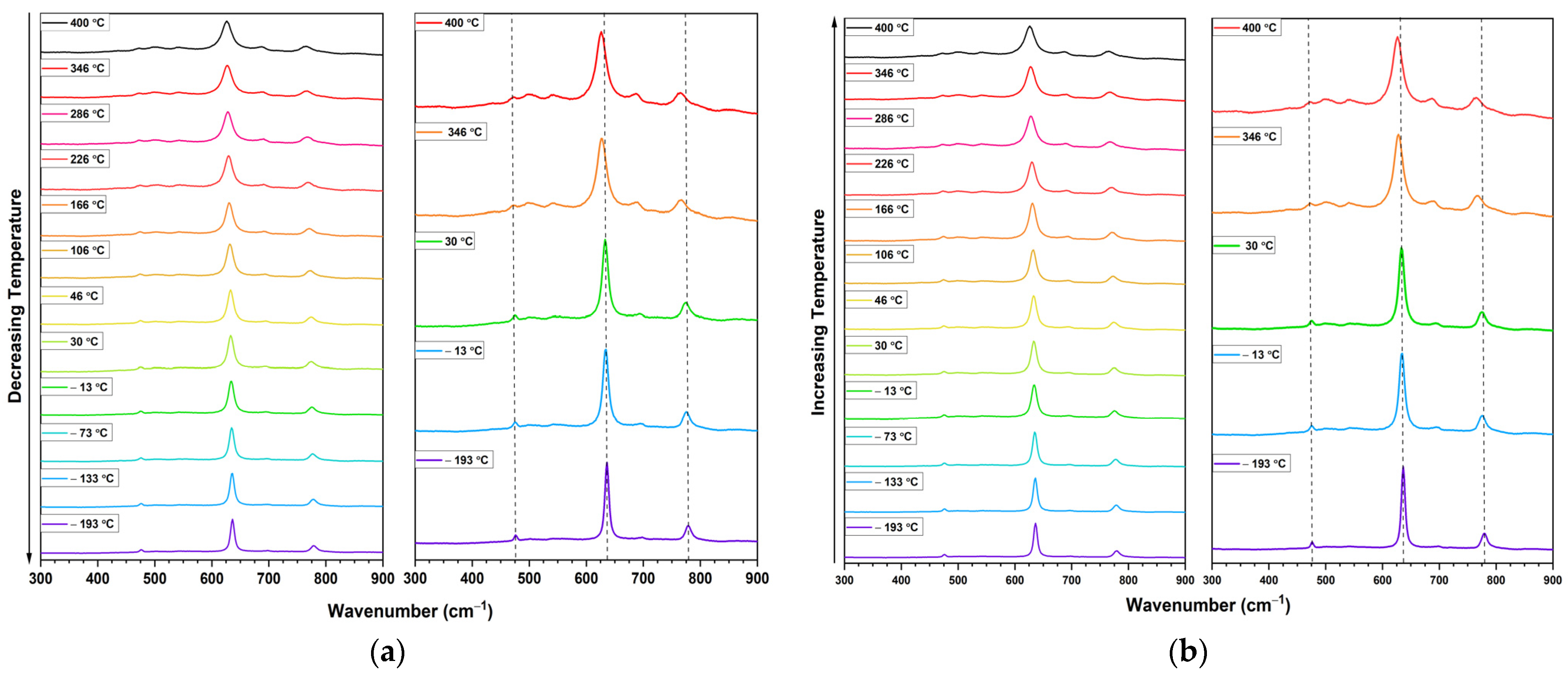
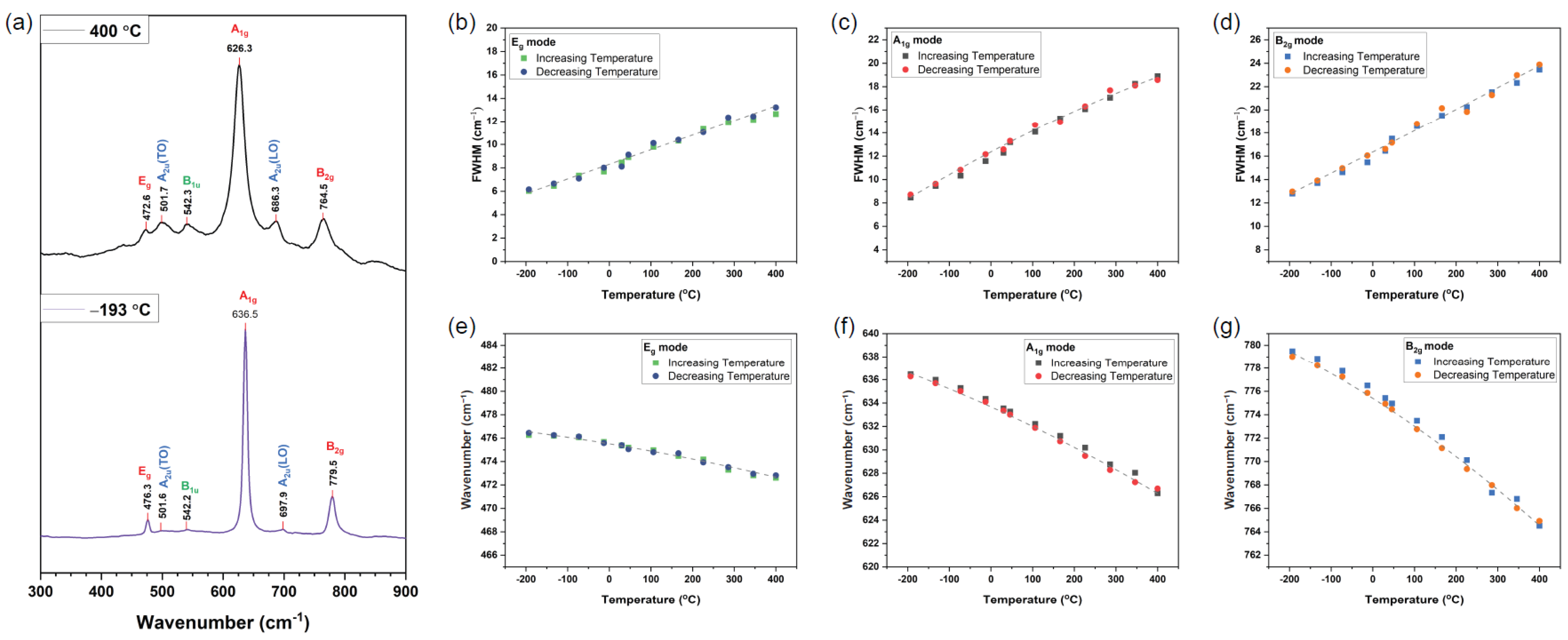
2.2. Raman Spectroscopy
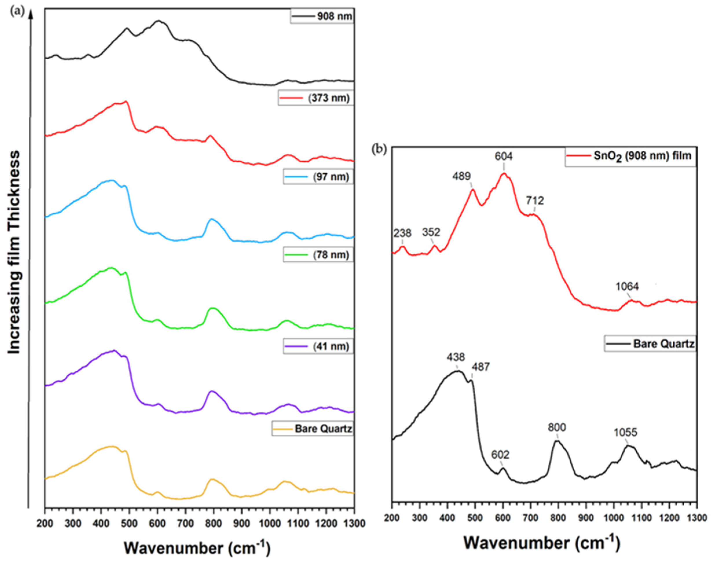
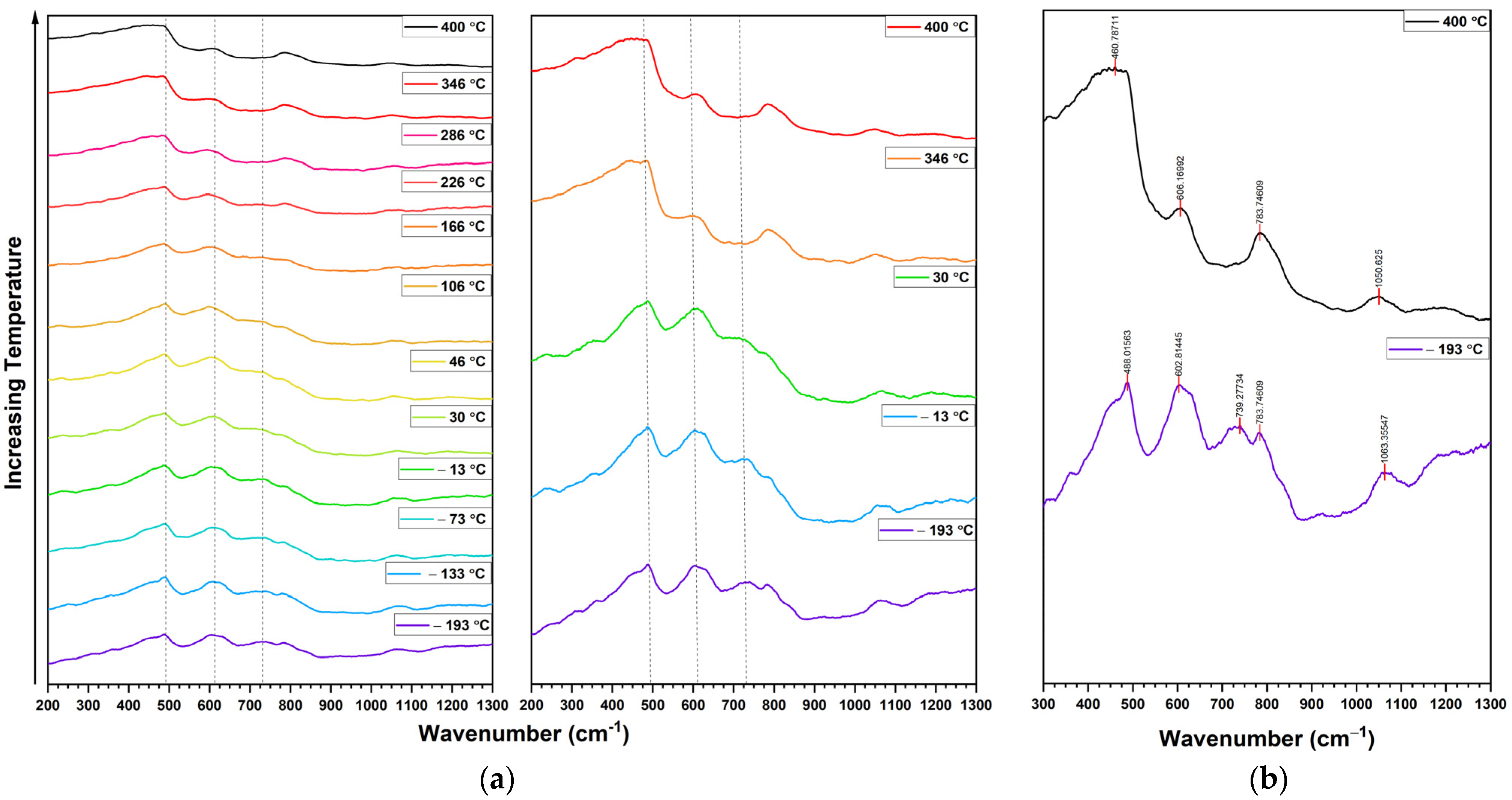
- It appeared that the 438 cm−1 Raman mode observed on bare quartz is close to the Zur et al. band of SiO2-SnO2 (transparent glass-ceramic) and could be assigned to vibrations of symmetric stretching of Si-O-Si bonds in six-membered rings which assigned to SiO4 tetrahedra deformation vibration [55,57]. The narrowing of the 438 cm−1 peak is due to the existence of SnO2 that could provoke a tighter Si-O-Si angle of SiO4 tetrahedra or obstruct the construction of higher-membered rings [55,58]. Another study by McMillan associates the narrowing of the peak along with the wavenumber shift to the tighter Si-O-Si angle that is for a more compact SiO2 structure. Therefore, adding SnO2 to SiO2 could have prevented the formation of higher-membered rings [61].
- The two peaks at 488 cm−1 and 602 cm−1 in SnO2 film and 487 cm−1 and 602 cm−1 in bare quartz are related to D1 and D2 defect bands that are assigned to the defects of 4-fold and 3-fold rings in the normal 6-fold rings of SnO2, respectively [55,57]. It also appears that the addition of SnO2 into the SiO2 matrix has modified the 438 cm−1 peak with a D1 defect band.
- A shoulder peak of 602 cm−1 in the SnO2 908 nm film at room temperature and at −193 °C around 623 cm−1 could be related to the addition of SnO2 to SiO2. This band is weak and overlaps with the D1 defect band due to the disorder of the SnO2 nanoparticle [55,62]. The broadening of the A1g peak is due to a smaller grain size in the film.
- The peak at 739 cm−1 is a shoulder peak of that at 783 cm−1, which only appeared at −193 °C and may be due to . This value is closer to the specified value in Lan et al. [56].
- Finally, the peak that appears on SnO2 film at 1063 cm−1 and on bare quartz at 1055 cm−1 is associated with the symmetric stretching of Si-O [55].
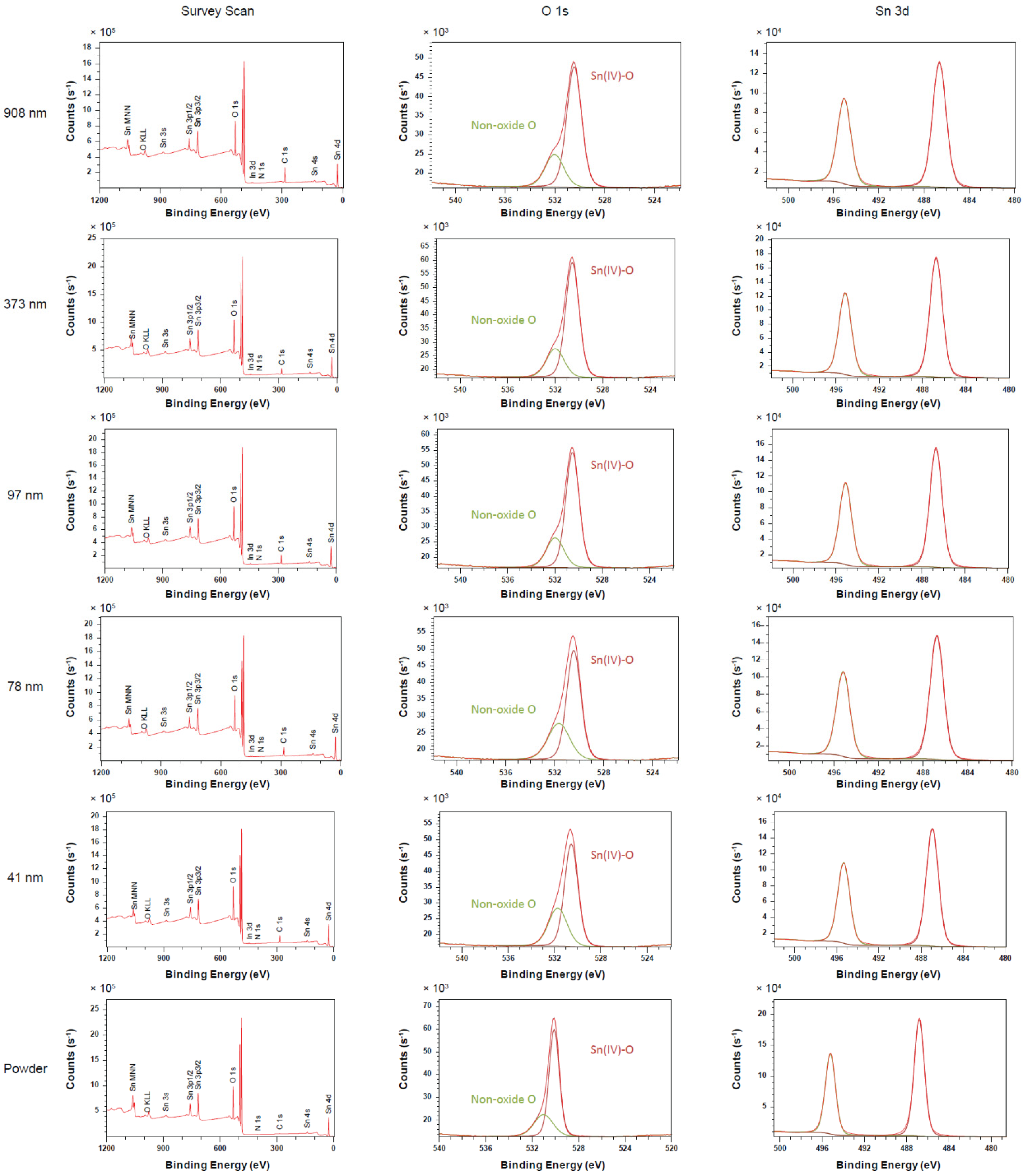
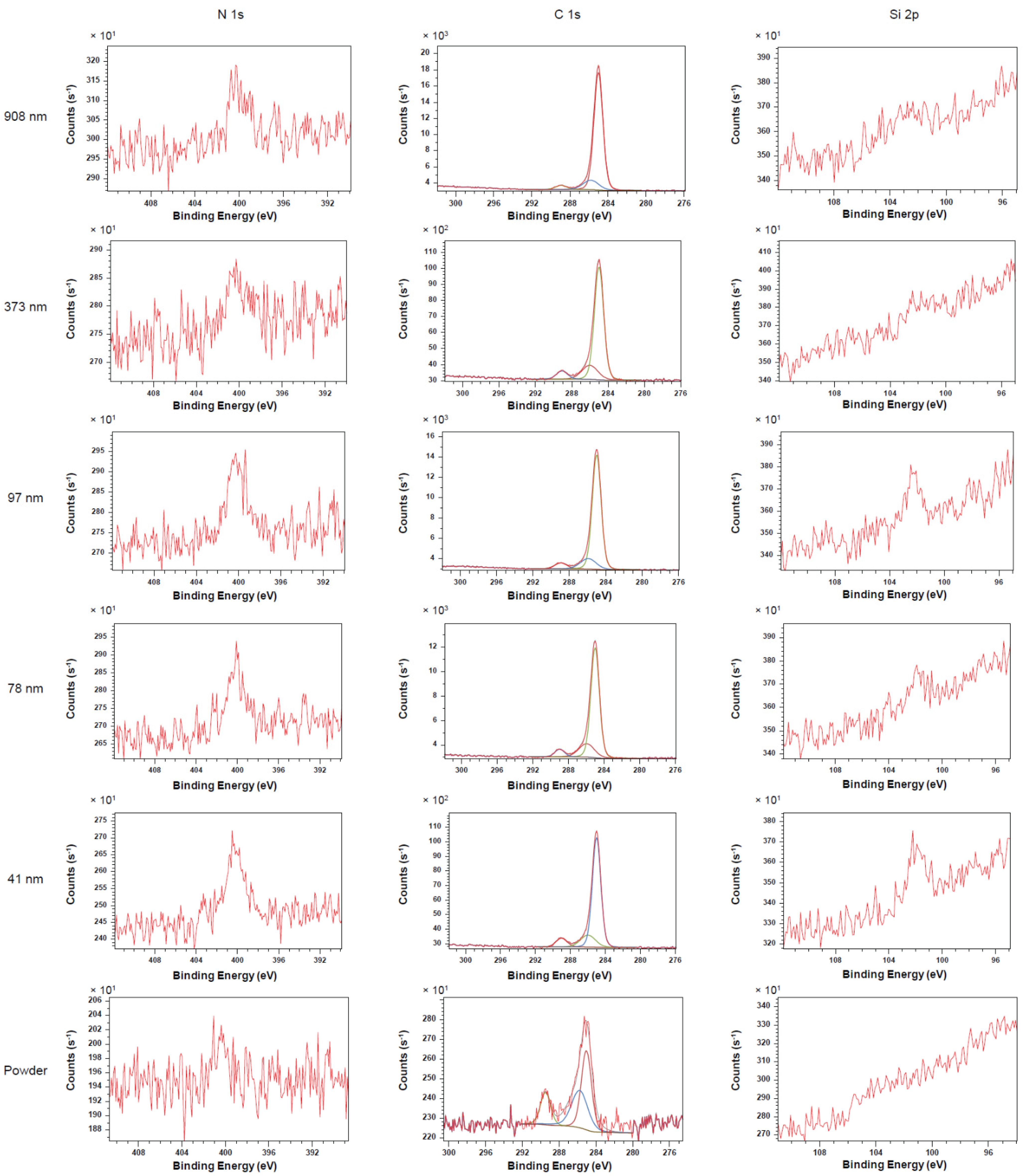
2.3. X-ray Photoelectron Spectroscopy
3. Methods
Author Contributions
Funding
Institutional Review Board Statement
Informed Consent Statement
Data Availability Statement
Acknowledgments
Conflicts of Interest
∂ Commercial equipment
# Though not an SI Unit
References
- Lee, I.; Choi, S.-J.; Park, K.-M.; Lee, S.S.; Choi, S.; Kim, I.-D.; Park, C.O. The stability, sensitivity and response transients of ZnO, SnO2 and WO3 sensors under acetone, toluene and H2S environments. Sens. Actuators B Chem. 2014, 197, 300–307. [Google Scholar] [CrossRef]
- Yuliarto, B.; Gumilar, G.; Septiani, N.L.W. SnO2 nanostructure as pollutant gas sensors: Synthesis, sensing performances, and mechanism. Adv. Mater. Sci. Eng. 2015, 2015, 694823. [Google Scholar] [CrossRef]
- Sharma, A.; Tomar, M.; Gupta, V. SnO2 thin film sensor with enhanced response for NO2 gas at lower temperatures. Sens. Actuators B Chem. 2011, 156, 743–752. [Google Scholar] [CrossRef]
- Gong, J.; Chen, Q.; Lian, M.-R.; Liu, N.-C.; Stevenson, R.G.; Adami, F. Micromachined nanocrystalline silver doped SnO2 H2S sensor. Sens. Actuators B Chem. 2006, 114, 32–39. [Google Scholar] [CrossRef]
- Korotcenkov, G.; Brinzari, V.; Cho, B.K. In2O3-and SnO2-based thin film ozone sensors: Fundamentals. J. Sens. 2016, 2016, 1–32. [Google Scholar] [CrossRef]
- Suman, P.H.; Felix, A.A.; Tuller, H.L.; Varela, J.A.; Orlandi, M.O. Comparative gas sensor response of SnO2, SnO and Sn3O4 nanobelts to NO2 and potential interferents. Sens. Actuators B Chem. 2015, 208, 122–127. [Google Scholar] [CrossRef]
- Mills, S.; Lim, M.; Lee, B.; Misra, V. Atomic layer deposition of SnO2 for selective room temperature low ppb level O3 sensing. ECS J. Solid State Sci. Technol. 2015, 4, S3059. [Google Scholar] [CrossRef]
- Kim, B.; Lu, Y.; Hannon, A.; Meyyappan, M.; Li, J. Low temperature Pd/SnO2 sensor for carbon monoxide detection. Sens. Actuators B Chem. 2013, 177, 770–775. [Google Scholar] [CrossRef]
- Vishwakarma, S.R.; Prasad, H.C. Low cost SnO2: P/SiO2/n-Si (textured) heterojunction solar cells. J. Phys. D Appl. Phys. 1993, 26, 959. [Google Scholar] [CrossRef]
- Vasu, V.; Subrahmanyam, A. Photovoltaic properties of indium tin oxide (ITO)/silicon junctions prepared by spray pyrolysis-dependence on oxidation time. Semiconductor Sci. Technol. 1992, 7, 320. [Google Scholar] [CrossRef]
- Ferlauto, A.S.; Ferreira, G.M.; Pearce, J.M.; Wronski, C.R.; Collins, R.W.; Deng, X.; Ganguly, G. Analytical model for the optical functions of amorphous semiconductors from the near-infrared to ultraviolet: Applications in thin film photovoltaics. J. Appl. Phys. 2002, 92, 2424–2436. [Google Scholar] [CrossRef]
- Tennakone, K.; Kumara, G.R.R.A.; Kottegoda, I.R.M.; Perera, V.P.S. An efficient dye-sensitized photoelectrochemical solar cell made from oxides of tin and zinc. Chem. Commun. 1999, 15–16. [Google Scholar] [CrossRef]
- Zheng, J.P.; Kwok, H.S. Preparation of indium tin oxide films at room temperature by pulsed laser deposition. Thin Solid Films 1993, 232, 99–104. [Google Scholar] [CrossRef]
- Ito, S.; Makari, Y.; Kitamura, T.; Wada, Y.; Yanagida, S. Fabrication and characterization of mesoporous SnO2/ZnO-composite electrodes for efficient dye solar cells. J. Mater. Chem. 2004, 14, 385–390. [Google Scholar] [CrossRef]
- Bagheri-Mohagheghi, M.M.; Shokooh-Saremi, M. The influence of Al doping on the electrical, optical and structural properties of SnO2 transparent conducting films deposited by the spray pyrolysis technique. J. Phys. D Appl. Phys. 2004, 37, 1248. [Google Scholar] [CrossRef]
- Liu, C.; Matsutani, T.; Yamamoto, N.; Kiuchi, M. High-quality indium tin oxide films prepared at room temperature by oxygen ion beam assisted deposition. EPL Europhys. Lett. 2002, 59, 606–611. [Google Scholar] [CrossRef]
- Reddy, V.S.; Das, K.; Dhar, A.; Ray, S.K. The effect of substrate temperature on the properties of ITO thin films for OLED applications. Semicond. Sci. Technol. 2006, 21, 1747–1752. [Google Scholar] [CrossRef]
- LavrenčičáŠtangar, U. Preparation and characterization of Mo-and Sb: Mo-doped SnO2 sol-gel-derived films for counter-electrode applications in electrochromic devices. J. Mater. Chem. 1995, 5, 617–624. [Google Scholar]
- Kityk, I.V.; Eboth, J.; Miedzinski, R.; Addou, M.; Sieder, H.; Karafiat, A. Optically-induced non-linear optical effects in indium–tin oxide crystalline films. Semicond. Sci. Technol. 2003, 18, 549–553. [Google Scholar] [CrossRef]
- Morgado, J.; Barbagallo, N.; Charas, A.; Matos, M.; Alcácer, L.; Cacialli, F. Self-assembly surface modified indium-tin oxide anodes for single-layer light-emitting diodes. J. Phys. D Appl. Phys. 2003, 36, 434–438. [Google Scholar] [CrossRef]
- Suzuki, T.; Yamazaki, T.; Oda, H. Effects of composition and thickness on the electrical properties of indium oxide/tin oxide multilayered films. J. Mater. Sci. 1989, 24, 1383. [Google Scholar] [CrossRef]
- Guillén, C.; Herrero, J. Influence of the film thickness on the structure, optical and electrical properties of ITO coatings deposited by sputtering at room temperature on glass and plastic substrates. Semicond. Sci. Technol. 2008, 23, 075002. [Google Scholar] [CrossRef]
- Munir, M.M.; Iskandar, F.; Yun, K.M.; Okuyama, K.; Abdullah, M. Optical and electrical properties of indium tin oxide nanofibers prepared by electrospinning. Nanotechnology 2008, 19, 145603. [Google Scholar] [CrossRef] [PubMed]
- Ferrere, S.; Zaban, A.; Gregg, B.A. Dye sensitization of nanocrystalline tin oxide by perylene derivatives. J. Phys. Chem. B 1997, 101, 4490–4493. [Google Scholar] [CrossRef]
- Huang, H.; Tan, O.K.; Lee, Y.C.; Tran, T.D.; Tse, M.S.; Yao, X. Semiconductor gas sensor based on tin oxide nanorods prepared by plasma-enhanced chemical vapor deposition with post plasma treatment. Appl. Phys. Lett. 2005, 87, 163123. [Google Scholar] [CrossRef]
- Varghese, O.K.; Malhotra, L.K. Electrode-sample capacitance effect on ethanol sensitivity of nano-grained SnO2 thin films. Sens. Actuators B Chem. 1998, 53, 19–23. [Google Scholar] [CrossRef]
- Sakanoue, T.; Nakatani, S.; Ueda, Y.; Izumi, H.; Ishihara, T.; Motoyama, M. Fabrication of well-ordered indium-tin-oxide film and characterization of organic films vacuum-deposited on it. Mol. Cryst. Liq. Cryst. 2003, 405, 59–66. [Google Scholar] [CrossRef]
- Khanna, A.; Kumar, R.; Bhatti, S.S. CuO doped SnO2 thin films as hydrogen sulfide gas sensor. Appl. Phys. Lett. 2003, 82, 4388. [Google Scholar] [CrossRef]
- Comini, E.; Faglia, G.; Sberveglieri, G.; Pan, Z.; Wang, Z.L. Stable and highly sensitive gas sensors based on semiconducting oxide nanobelts. Appl. Phys. Lett. 2002, 81, 1869–1871. [Google Scholar] [CrossRef]
- Song, J.E.; Lee, D.K.; Kim, Y.H.; Kang, Y.S. Preparation of water dispersed indium tin oxide sol solution. Mol. Cryst. Liq. Cryst. 2006, 444, 247–255. [Google Scholar] [CrossRef]
- Coles, G.S.V.; Williams, G.; Smith, B.J. The effect of oxygen partial pressure on the response of tin (IV) oxide based gas sensors. J. Phys. D Appl. Phys. 1991, 24, 633–641. [Google Scholar] [CrossRef]
- Panchapakesan, B.; DeVoe, D.L.; Widmaier, M.R.; Cavicchi, R.; Semancik, S. Nanoparticle engineering and control of tin oxide microstructures for chemical microsensor applications. Nanotechnology 2001, 12, 336–349. [Google Scholar] [CrossRef]
- Choi, Y.J.; Hwang, I.-S.; Park, J.-G.; Choi, K.J.; Park, J.H.; Lee, J.-H. Novel fabrication of an SnO2 nanowire gas sensor with high sensitivity. Nanotechnology 2008, 19, 095508. [Google Scholar] [CrossRef]
- Eastwood, P.G.; Claypole, T.C.; Watson, J.; Coles, G.S.V. The behaviour of tin dioxide sensors in exhaust environments at low and intermediate temperatures. Meas. Sci. Technol. 1993, 4, 524–533. [Google Scholar] [CrossRef]
- Llobet, E.; Vilanova, X.; Brezmes, J.; Alcubilla, R.; Calderer, J.; Sueiras, J.E.; Corrie, X. Conductance-transient analysis of thick-film tin oxide gas sensors under successive gas-injection steps. Meas. Sci. Technol. 1997, 8, 1133–1138. [Google Scholar] [CrossRef]
- Partridge, J.G.; Field, M.R.; Peng, J.L.; Sadek, A.Z.; Kalantar-zadeh, K.; Du Plessis, J.; McCulloch, D.G. Nanostructured SnO2 films prepared from evaporated Sn and their application as gas sensors. Nanotechnology 2008, 19, 125504. [Google Scholar] [CrossRef]
- Colomban, P.; Gironda, M.; Franci, G.S.; d’Abrigeon, P. Distinguishing Genuine Imperial Qing Dynasty Porcelain from Ancient Replicas by On-Site Non-Invasive XRF and Raman Spectroscopy. Materials 2022, 15, 5747. [Google Scholar] [CrossRef]
- Alamrani, F.; Alsharaeh, E. Controlling the Bandgaps of One-Dimensional TiO2/SiO2, TiO2/SnO2, and SiO2/SnO2 Photonic Crystals Using the Transfer Matrix Method. Optics Photon. J. 2022, 12, 171–189. [Google Scholar] [CrossRef]
- Gotschy, W.; Vonmetz, K.; Leitner, A.; Aussenegg, F.R. Thin films by regular patterns of metal nanoparticles: Tailoring the optical properties by nanodesign. Appl. Phys. B 1996, 63, 381–384. [Google Scholar] [CrossRef]
- Dhatarwal, P.; Sengwa, R.J.; Choudhary, S. Multifunctional (PVP/PEO)/SnO2 nanocomposites of tunable optical and dielectric properties. Optik 2020, 221, 165368. [Google Scholar] [CrossRef]
- Kavan, L. Conduction band engineering in semiconducting oxides (TiO2, SnO2): Applications in perovskite photovoltaics and beyond. Catal. Today 2019, 328, 50–56. [Google Scholar] [CrossRef]
- Subbiah, A.S.; Mathews, N.; Mhaisalkar, S.G.; Sarkar, S.K. Novel Plasma-assisted low-temperature-processed SnO2 thin films for efficient flexible perovskite photovoltaics. ACS Energy Lett. 2018, 3, 1482–1491. [Google Scholar] [CrossRef]
- Dalapati, G.K.; Sharma, H.; Guchhait, A.; Chakrabarty, N.; Bamola, P.; Liu, Q.; Saianand, G.; Krishna, A.M.S.; Mukhopadhyay, S.; Dey, A.; et al. Tin oxide for optoelectronic, photovoltaic and energy storage devices: A review. J. Mater. Chem. A 2021, 9, 16621–16684. [Google Scholar] [CrossRef]
- Yu, H.; Yeom, H.-I.; Lee, J.W.; Lee, K.; Hwang, D.; Yun, J.; Ryu, J.; Lee, J.; Bae, S.; Kim, S.K.; et al. Superfast room-temperature activation of SnO2 thin films via atmospheric plasma oxidation and their application in planar perovskite photovoltaics. Adv. Mater. 2018, 30, 1704825. [Google Scholar] [CrossRef]
- Pyke, D.R.; Reid, R.; Tilley, R.J.D. Structures of tin oxide—antimony oxide catalysts. J. Chem. Soc. Faraday Trans. 1 Phys. Chem. Condens. Phases 1980, 76, 1174–1182. [Google Scholar] [CrossRef]
- Dodd, A.; McKinley, A.; Saunders, M.; Tsuzuki, T. Mechanochemical synthesis of nanocrystalline SnO2–ZnO photocatalysts. Nanotechnology 2006, 17, 692. [Google Scholar] [CrossRef]
- Cai, X.; Ogorevc, B.; Tavčar, G.; Wang, J. Indium—Tin oxide film electrode as catalytic amperometric sensor for hydrogen peroxide. Analyst 1995, 120, 2579–2583. [Google Scholar] [CrossRef]
- Jyothi, T.M.; Sugunan, S.; Rao, B.S. Selective methylation of anisole to 2,6-xylenol over rare earth promoted SnO2 catalysts. Green Chem. 2000, 2, 269–271. [Google Scholar] [CrossRef]
- Bond, G.C.; Molloy, L.R.; Fuller, M.J. Oxidation of carbon monoxide over palladium—tin(IV) oxide catalysts: An example of spillover catalysis. J. Chem. Soc. Chem. Commun. 1975, 796–797. [Google Scholar] [CrossRef]
- Hines, R.I.; Allan, N.L.; Flavell, W.R. Oxidation catalysts: A comparative simulation study of the lattice, defect and surface structure of the stannates ASnO3(A = Ca, Sr and Ba) and SnO2. J. Chem. Soc. Faraday Trans. 1996, 92, 2057–2063. [Google Scholar] [CrossRef]
- He, Z.-K.; Sun, Q.; Xie, K.; Lu, P.; Shi, Z.; Kamali, A.R. Reactive molten salt synthesis of natural graphite flakes decorated with SnO2 nanorods as high performance, low cost anode material for lithium ion batteries. J. Alloy. Compd. 2019, 792, 1213–1222. [Google Scholar] [CrossRef]
- Kohl, D.; Thoren, W.; Schnakenberg, U.; Schüll, G.; Heiland, G. Decomposition of gaseous acetic acid on SnO2. J. Chem. Soc. Faraday Trans. 1991, 87, 2647–2653. [Google Scholar] [CrossRef]
- Bonu, V.; Das, A.; Sivadasan, A.K.; Tyagi, A.K.; Dhara, S. Invoking forbidden modes in SnO2 nanoparticles using tip enhanced Raman spectroscopy. J. Raman Spectrosc. 2015, 46, 1037–1040. [Google Scholar] [CrossRef]
- Bhadrapriya, B.C.; Varghese, A.R.; Amarendra, G.; Hussain, S. Sb:SnO2 thin films—Synthesis and characterization. AIP Conf. Proc. 2018, 1951, 030006. [Google Scholar]
- Zur, L.; Tran, L.T.N.; Massella, D.; Vaccari, A.; Chiappini, A.; Chiasera, A.; Varas, S.; Armellini, C.; Carpentiero, A.; Boulard, B.; et al. SiO2-SnO2 transparent glass-ceramics activated by rare earth ions. Opt. Compon. Mater. 2019, 10914, 180–188. [Google Scholar]
- Lan, T.; Li, C.W.; Fultz, B. Phonon anharmonicity of rutile SnO2 studied by Raman spectrometry and first principles calculations of the kinematics of phonon-phonon interactions. Phys. Rev. B 2012, 86, 134302. [Google Scholar] [CrossRef]
- Manghnani, M.H.; Hushur, A.; Sekine, T.; Wu, J.; Stebbins, J.F.; Williams, Q. Raman, Brillouin, and nuclear magnetic resonance spectroscopic studies on shocked borosilicate glass. J. Appl. Phys. 2011, 109, 113509. [Google Scholar] [CrossRef]
- Van Tran, T.; Turrell, S.; Eddafi, M.; Capoen, B.; Bouazaoui, M.; Roussel, P.; Berneschi, S.; Righini, G.C.; Ferrari, M.; Bhaktha, S.N.B.; et al. Investigations of the effects of the growth of SnO2 nanoparticles on the structural properties of glass–ceramic planar waveguides using Raman and FTIR spectroscopies. J. Mol. Struct. 2010, 976, 314–319. [Google Scholar] [CrossRef]
- Gouvêa, D.; Pereira, G.J.; Gengembre, L.; Steil, M.C.; Roussel, P.; Rubbens, A.; Hidalgo, P.; Castro, R.H. Quantification of MgO surface excess on the SnO2 nanoparticles and relationship with nanostability and growth. Appl. Surf. Sci. 2011, 257, 4219–4226. [Google Scholar] [CrossRef]
- Kamali, A.R.; Fray, D.J. Solid phase growth of tin oxide nanostructures. Mater. Sci. Eng. B 2012, 177, 819–825. [Google Scholar] [CrossRef]
- McMillan, P.F.; Remmele, R.L. Hydroxyl sites in SiO2 glass: A note on infrared and Raman spectra. Am. Mineral. 1986, 71, 772–778. [Google Scholar]
- Van Tran, T.T.; Bui, T.S.; Turrell, S.; Capoen, B.; Roussel, P.; Bouazaoui, M.; Ferrari, M.; Cristini, O.; Kinowski, C. Controlled SnO2 nanocrystal growth in SiO2-SnO2 glass-ceramic monoliths. J. Raman Spectrosc. 2012, 43, 869–875. [Google Scholar] [CrossRef]
- Saji, K.J.; Mary, A.P.R. Tin oxide based p and n-type thin film transistors developed by RF sputtering. ECS J. Solid State Sci. Technol. 2015, 4, Q101–Q104. [Google Scholar] [CrossRef]
- Alghamdi, H.; Concepcion, B.; Baliga, S.; Misra, P. Synthesis, spectroscopic characterization and applications of tin dioxide. In Contemporary Nanomaterials in Material Engineering Applications; Springer: Cham, Switzerland, 2021; pp. 285–318. [Google Scholar]


| Modes (All Units cm−1) | 908 nm Film | Bare Quartz | Zur et al. [55] | Modes | SnO2 Powder | ||
|---|---|---|---|---|---|---|---|
| Ambient Condition | –193 °C | 400 °C | 30 °C | –193 °C | 400 °C | ||
| Si-O-Si (symmetric stretching) | — | 438 | 440 | — | — | ||
| D1 defect bands | 488 460 | 487 | 489 | Eg | 476 472 | ||
| — | — | — | — | A2u(TO) | 501 | ||
| — | — | — | — | B1u | 542 | ||
| D2 defect bands | 602 606 | 602 | 600 | A1g | 636 626 | ||
| — | — | — | — | A2u(LO) | 697 686 | ||
| 739 — | — | — | — | — | |||
| O-Si-O (symmetric stretching) | 783 | 800 | 800 | B2g | 779 764 | ||
| Si-O (symmetric stretching) | 1063 1050 | 1055 | — | — | — | ||
| Sample Peak Positions (Averaged, with 1σ Error from Peak Fitting) | ||||
|---|---|---|---|---|
| Sample Type | Sn 3d 5/2 | Sn 3d 3/2 | O 1s (Oxide) | O 1s (Non-Oxide) |
| 908 nm | 486.65 ± 0.02 | 495.07 ± 0.02 | 530.48 ± 0.03 | 532.05 ± 0.02 |
| 373 nm | 486. 74 ± 0.02 | 495.16 ± 0.02 | 530.57 ± 0.03 | 532.03 ± 0.05 |
| 97 nm | 486.71 ± 0.01 | 495.12 ± 0.01 | 530.52 ± 0.02 | 531.98 ± 0.03 |
| 78 nm | 486.80 ± 0.04 | 495.21 ± 0.04 | 530.48 ± 0.04 | 531.73 ± 0.06 |
| 41 nm | 486.90 ± 0.03 | 495.31 ± 0.03 | 530.53 ± 0.03 | 531.66 ± 0.08 |
| Powder | 486.81 ± 0.13 | 495.23 ± 0.14 | 530.49 ± 0.36 | 531.40 ± 0.35 |
| Sample Elemental Percentages (Averaged, with 1σ Error from Peak Fitting) | ||||
|---|---|---|---|---|
| Sample Type | Sn % | Oxide O % | Non-Oxide O % | Total O % |
| 908 nm | 37.75 ± 0.25 | 46.43 ± 0.41 | 15.81 ± 0.66 | 62.24 ± 0.26 |
| 373 nm | 38.31 ± 0.19 | 46.62 ± 0.50 | 15.02 ± 0.39 | 61.69 ± 0.19 |
| 97 nm | 37.79 ± 0.41 | 46.03 ± 1.29 | 16.19 ± 1.69 | 62.21 ± 0.41 |
| 78 nm | 38.27 ± 0.15 | 42.17 ± 0.87 | 19.55 ± 1.02 | 61.73 ± 0.15 |
| 41 nm | 37.83 ± 0.02 | 40.44 ± 1.16 | 21.73 ± 1.18 | 62.17 ± 0.02 |
| Powder | 40.06 ± 0.20 | 43.44 ± 0.24 | 16.49 ± 0.12 | 59.93 ± 0.20 |
Disclaimer/Publisher’s Note: The statements, opinions and data contained in all publications are solely those of the individual author(s) and contributor(s) and not of MDPI and/or the editor(s). MDPI and/or the editor(s) disclaim responsibility for any injury to people or property resulting from any ideas, methods, instructions or products referred to in the content. |
© 2023 by the authors. Licensee MDPI, Basel, Switzerland. This article is an open access article distributed under the terms and conditions of the Creative Commons Attribution (CC BY) license (https://creativecommons.org/licenses/by/4.0/).
Share and Cite
Alghamdi, H.; Farinre, O.Z.; Kelley, M.L.; Biacchi, A.J.; Saha, D.; Adel, T.; Siebein, K.; Walker, A.R.H.; Hacker, C.A.; Rigosi, A.F.; et al. Experimental Spectroscopic Data of SnO2 Films and Powder. Data 2023, 8, 37. https://doi.org/10.3390/data8020037
Alghamdi H, Farinre OZ, Kelley ML, Biacchi AJ, Saha D, Adel T, Siebein K, Walker ARH, Hacker CA, Rigosi AF, et al. Experimental Spectroscopic Data of SnO2 Films and Powder. Data. 2023; 8(2):37. https://doi.org/10.3390/data8020037
Chicago/Turabian StyleAlghamdi, Hawazin, Olasunbo Z. Farinre, Mathew L. Kelley, Adam J. Biacchi, Dipanjan Saha, Tehseen Adel, Kerry Siebein, Angela R. Hight Walker, Christina A. Hacker, Albert F. Rigosi, and et al. 2023. "Experimental Spectroscopic Data of SnO2 Films and Powder" Data 8, no. 2: 37. https://doi.org/10.3390/data8020037