Review

Modulators in Silicon Photonics—Heterogenous Integration & and Beyond

1
Physics Department, University College Cork, T12 XF62 Cork, Ireland
2
Integrated Photonics Group, Tyndall National Institute, Lee Maltings, T12 R5CP Cork, Ireland
*
Author to whom correspondence should be addressed.
Photonics 2022, 9(1), 40; https://doi.org/10.3390/photonics9010040
Submission received: 22 October 2021 / Revised: 20 December 2021 / Accepted: 5 January 2022 / Published: 12 January 2022
(This article belongs to the Special Issue Optical Technologies for Data Center Networks)

Abstract

:
The article below presents a review of current research on silicon photonics. Herein, an overview of current silicon modulator types and modern integration approaches is presented including direct bonding methods and micro-transfer printing. An analysis of current state of the art silicon modulators is also given. Finally, new prospects for III–V-silicon integration are explored and the prospects of an integrated modulator compatible with current CMOS processing is investigated.

1. Introduction

The presence of photonics in communications was spawned from the limitations of electrical communications and as the industry becomes more established optical technology is poised to be at the forefront of short-reach interconnects. The leading candidate in this revolution is silicon photonics, with the optical modulator being a key component. Modulators have seen a steady improvement in recent years from mega-hertz operation to post 100 GHz bandwidths becoming tangible achievements [1]. Silicon photonics provides major benefits for integration into more established commercial processing due to its inherent compatibility with mature Complementary Metal-Oxide-Semiconductor (CMOS) facilities. CMOS processing is well established with a high yield, low cost manufacturing with high reproducibility compared to other photonic platforms. The Silicon-on-Insulator platform already offers a wide array of photonic components [2,3,4] but Silicon’s indirect bandgap has made an efficient Silicon laser a major challenge.
With increased interest in silicon lasers, increased research seeks to demonstrate silicon’s suitability as the preferred optical platform. Silicon is limited compared to more established III–V materials such as InP and GaAs in the field of photonics. Silicon optical technology extends beyond just lasers, offering photonic components such as, modulators, photodetectors (PDs), splitters, (de)multiplexers, and filters. Each of these components is in itself a breakthrough of engineering, utilizing either the innate physical properties of Silicon or clever utilization of alternate methods to overcome Silicon’s optical pitfalls [5]. Silicon modulators, for example, utilize a free carrier plasma dispersion effect; wherein devices in silicon photonics use implanted dopants for optical phase and amplitude modulation via a material with excess electrons or holes undergoes a wavelength dependent change in complex refractive index. Thus, by altering the free carrier concentration in a waveguide the phase and amplitude of the light within can be modulated. Mach-Zehnder interferometric (MZI) and ring-based modulators have been reported [6,7,8] with speeds of 18 Gbps being attained under forward bias operation [9,10]. Reverse bias operation achieved 30 GHz of bandwidth [11,12,13]. Sun et al. even demonstrates a reverse biased microring modulator (MRM) up to speeds of up to 128 Gb/s [14].
The primary purpose of this review is to analyze the current methods of marrying the benefits of III–V materials and Silicon to produce a viable modulator that is capable of satisfying all the requirements of a modern optical data transmission on Silicon, in a manner which is competitive with modulators made purely on Silicon.

2. The Mechanics of Modulator Types

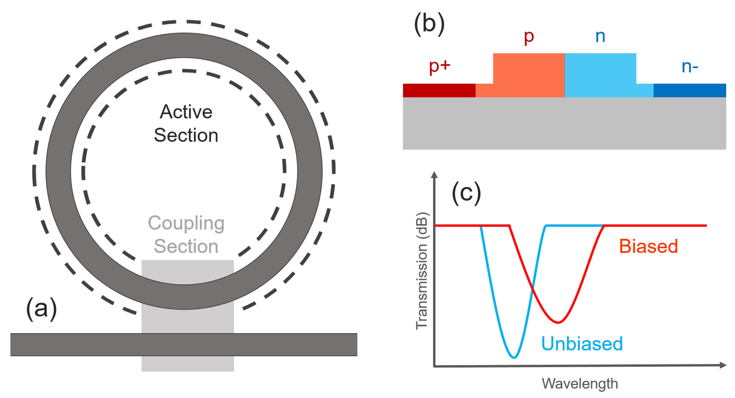
2.1. Ring Modulators

Ring resonators have played a very prevalent role in the field of silicon modulators. In general, a ring resonator consists of a closed loop optical waveguide, which creates a resonant condition for wavelengths which are a whole number of the optical path length. Typically, there are many wavelengths which satisfy this condition which leads to a ring having multiple resonances. The spacing between these resonances is dependent on the length of the ring resonator and is referred to as the free spectral range (FSR), which is commonly expressed in GHz or nm.
A ring resonator is only useful when light can be coupled in and out of the resonant cavity. The most common method of coupling is codirectional evanescent coupling between the ring and an adjacent waveguide [15]. A resonator is a passive device but a ring can also be used as an active device such as a modulator. In a ring modulator the resonator is made to align the operating wavelength with the resonance peak. In this way, modulating the optical path length of the ring shifts the resonance peak. This phenomenon is illustrated in Figure 1 [15]. High speed modulation has been demonstrated many times over with ring resonators via shifting the carrier density of the material, changing the refractive index [16], and therefore the resonance wavelength through the application of an external voltage to the device’s PN junction [8,17].
In operation, the primary benefits of the silicon ring modulator, also referred to as a micro-ring modulator (MRM) due to the devices’ small scale, are its small footprint, low power consumption, and narrow wavelength selectivity [18]. The challenges of silicon MRMs stems from silicon’s third order non linearity [19], which generates nonlinear effects, resulting in carrier [20] and thermal [21] induced optical bistabilities and self pulsation from these phenomena acting in competition to each other [22].

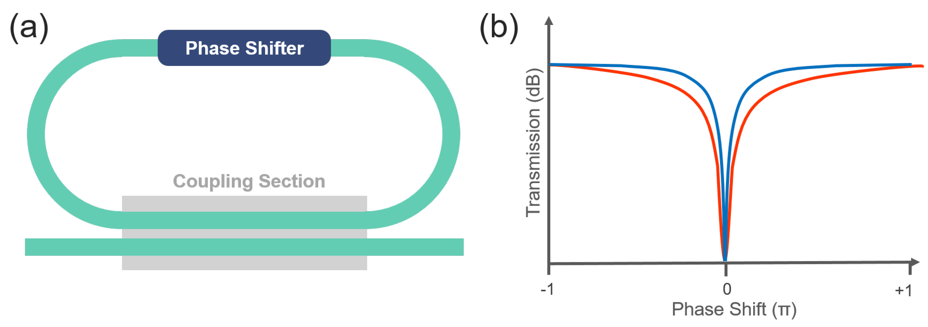
2.2. Mach-Zehnder Modulators (MZM)

Mach-Zehnder Modulators (MZMs) are another common optical modulator. MZMs are based on the original concept of a Mach-Zehnder Interferometer (MZI), which relies on separating light into two optical paths at some form of input coupler. the light travelling in one or both of these pathways can then have its phase modulated before the paths recombine and interference occurs. In the case of most semiconductors, the pathway arms of the MZM are usually equipped with phase modulators reliant on a drive voltage, with the voltage difference between full positive and negative interferences being denoted as the switching voltage; V π . The phase difference for this condition being a difference of π between the phase of the light in the two arms.
MZMs can be noted for their high-contrast optical transmission without deterioration due to spectral broadening and frequency chirping [23,24,25,26]. In silicon photonics the monolothic integration of MZMs with other photonic components such as photodiodes is achievable with fabrication technologies to create integrated devices with small footprints [26,27,28]. In silicon MZMs the method of modulation relies on high speed refractive index modulation via free carrier plasma dispersion, or the carrier-refraction effect. This effect sees major usage in unstrained silicon and germanium where the Pockels effect; the voltage controlled phase delay in crystals, is not observed. Unstrained silicon is specified here as the Pockels effect has been recorded in strained silicon waveguides, although large voltages are required to achieve notable modulation [29]. Free carrier plasma dispersion has been used to design and model a wide range of silicon-based phase shifters [27]. Silicon optical modulators based on carrier dispersion effects typically use a PIN or PN diode structure across the optical waveguide to alter the density of free carriers available to interact with light within the guide [30]. Alternatively, demonstrations have been made which use the accumulation of free carriers around a thin dielectric layer in the waveguide [31]. PN junction based MZM modulators benefit from simple fabrication and high-speed performance but lack the modulation efficiency of the carrier injection and accumulation techniques.
Reed et al. presents a PN MZM with modulation efficiency ranging between 1.4 to 1.9 V/cm over reverse bias voltages between 0 and 6 V. An insertion loss of 5 dB was measured with 4dB being attributed to the phase modulator and 1 dB loss from the splitter and combiner. A speed of 52 Gb/s was demonstrated [32].
Xiao et al. demonstrates modulation speeds of up to 60 Gb/s in a silicon MZM using doping optimisation. A modulation efficiency of 2 V·cm was recorded with a maximum insertion loss of 3.5 dB [33].

2.3. Electro-Absorption Modulators (EAMs)

An electro-absorption modulator is a semiconductor PIN structure whose bandgap can be varied through the application of an external voltage, altering the devices absorption properties [34]. EAMs generally offer low drive voltages (∼2 V) and are cost effective in volume production. In effect, an EAM can be considered the opposite of a semiconductor laser diode. Both can be made on a semiconductor waveguide, forward bias producing photons and reverse bias absorbing them. Unfortunately this makes creating an effective pure silicon EAM incredibly challenging due to silicon’s indirect bandgap. The modulation in EAMs is achieved via the Quantum Confined Stark Effect (QCSE), which describes the change in light absorption spectrum of a quantum well material in response to an applied external electric field. The electric field causes electron states to shift to lower energies, and holes to higher energies.
Jeong et al. explores this challenge in a unique manner, incorporating homogeneous EAMs based on the aforementioned free carrier plasma dispersion effect [35]. Jeong utilises a Schottky diode as part of the EAM, achieving optical modulation by the intensity change of the light from the free carrier absorption to change the absorption coefficient, but not conventional interference effects. With this, 3 dB modulation depth was achieved at 6 V p p from 1542 to 1558 nm for EAMs with length 500 μ m.

3. III–V Hybrid Modulators

The advent of heterogeneous PIC integration has introduced a plethora of possibilities for improvements to the optical components now available on the Silicon platform. Lasers have been demonstrated but are only one of the key components of a high speed optical transmitter, thus modulators must also be considered. Modulators formed from the integration of III–V materials and Silicon typically use metal oxide semiconductor modulators as they provide a good balance of modulation bandwidth and efficiency [36,37]. In the modulators presented, n-doped InGaAsP is bonded to a p-doped Si layer with an insulating layer separating the two. This results in a Semiconductor-Insulator-Semiconductor-CAPacitor (SISCAP) formation. The SIS configuration behaves like a capacitor with the semiconductors acting as the plates and the insulating layer acting as a capacitive area between. This structure causes charge to accumulate, which alters the refractive index.
In Drude’s model, the change in refractive index, Δ n, caused by plasma dispersion is inversely proportional to the effective masses of holes and electrons [37]. The lighter n-doped III–V electrons result in a stronger electron-induced refractive index change when compared to Silicon [36]. Additionally, n-doped III–V materials provide a higher refractive index change per change in absorption coefficient, Δ k [36]. The result is a phase modulator with reduced spurious intensity modulation. This behavior is also true for p-doped III–V materials for carrier concentrations above 10 19 cm 3 , and below this threshold p-doped Silicon provides a better ratio of Δ n/ Δ k [36,37]. A hybrid III–V/Si MOS modulator can merge the best of III–V and Silicon. Consequently, this approach offers modulators with up to 5 times better modulation efficiency, and a lower phase shifter loss than all-silicon MOS modulators [36,37].
Other methods of integrating Silicon and III–V MOS modulators exist. By implementing a III–V on Si MOS modulator in a ring coupled to a straight waveguide in a race-track pattern, the energy consumption of a 40-GHz modulator can be 3.7 times better than III–V on Si MZMs. This can be accomplished while maintaining a modulation efficiency of 0.064 V·cm. A schematic representation of this design is presented in Figure 2 [38]. The 100- μ m-long phase shifter section of the modulator is made using a thin aluminum oxide gate layer separating the n-doped III–V and the p-doped Silicon layers. A proof-of-concept, taper-less integration of a few tens of nanometers thick III–V layer with Silicon has been shown to reduce the footprint and loss of the device with-out compromising the modulation efficiency of the III–V on Si MOS capacitor [39].
Electro-absorption modulators (EAMs) have been reported by the bonding of III–V QWs with silicon [40,41]. These EAMs use a PIN structure. By applying a bias voltage, the absorption of the material’s quantum wells can be altered via the Quantum Con-fined Stark Effect (QCSE) [41]. A segmented electrode, comprising a low-impedance active modulation section cascaded by a high-impedance passive section, provides high-bandwidth operation while ensuring low reflection and good modulation efficiency [41]. An over 67 GHz bandwidth hybrid III–V on silicon EAM utilizing this method has been fabricated.In the O-band, this modulator has an insertion loss of 4.9 dB, and it shows >9 dB of dynamic ER for 50 Gb/s operation over a 16-km long optical fiber link. III–V on Si modulators have shown good modulation efficiency with low-loss, but so far devices of a notably higher speed (∼100 Gb/s) have yet to be experimentally verified.

4. Integration Approaches
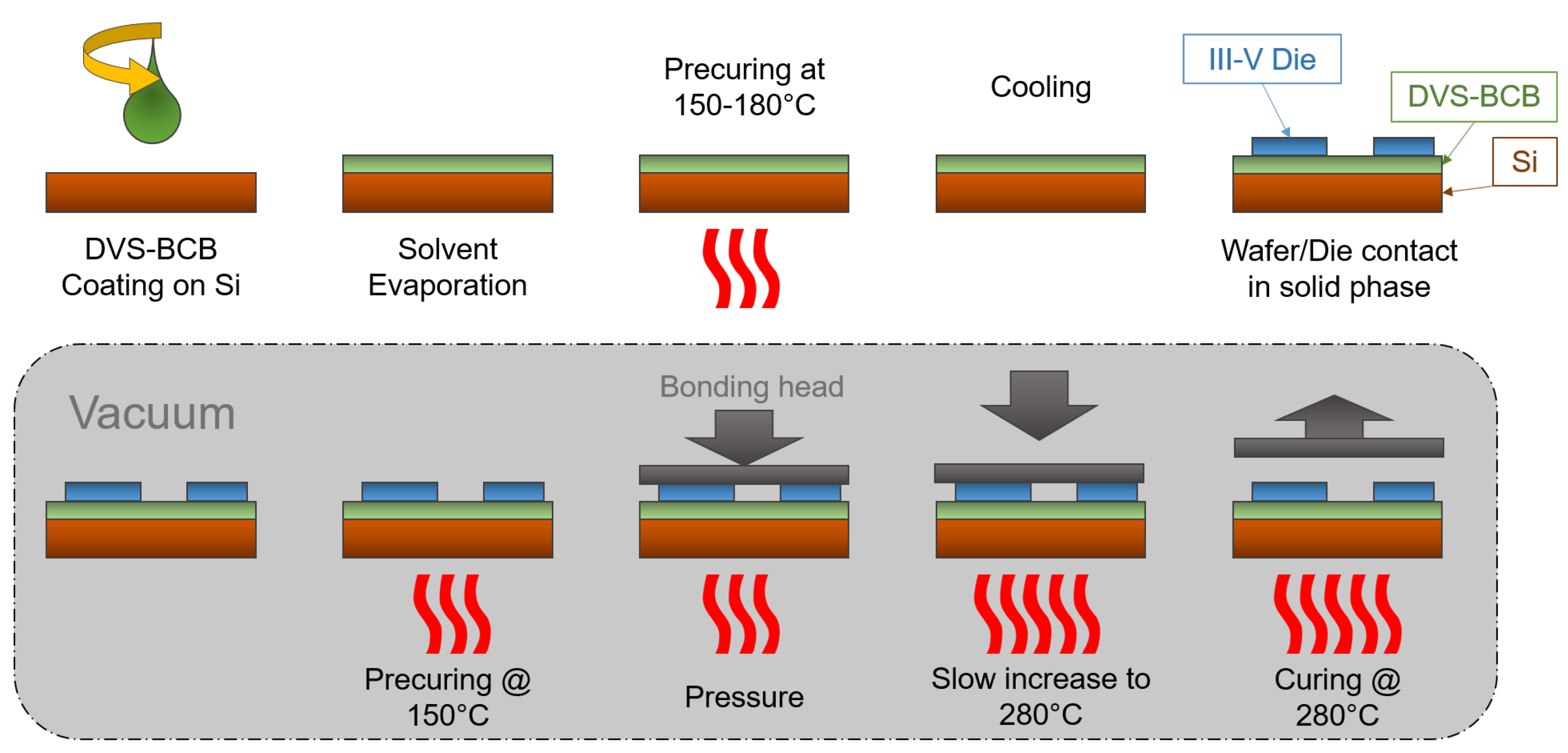
4.1. Bonding

Today, there exist many methods of combining III–V semiconductor devices with Silicon PICs. One such popular example is known as flip-chip bonding (FCB), wherein prefabricated optoelectronic devices, such as a laser, are bonded upside down on a substrate which has been prepared to receive this chip [42]. In FCB pre-processed III–V devices are normally flipped, however in such a case the alignment requirements slow the process down, adding to the cost. When seeking to minimize these costs, one seeks to reduce the overall length and time of the process as well as the amount of III–V material needing to be used due to the increased price of III–V material when compared to Silicon. Roelkens’ proposal of a die-to-wafer bonding in which unprocessed III–V dies are bonded, epitaxial layers down, to the processed Silicon, seeks to solve these issues of alignment and wastage [43]. The primary benefit of this technique is the reduced need for accuracy in terms of bonding due to the lack of structures on the die, which can improve process turnaround when compared to classic FCB. Additionally, reduced material consumption improves the cost of the process, as III–V semiconductors are only bonded where they are needed.
For the bonding process several different approaches have been explored. Roelkens et al. [43] utilised an adhesive die-to-wafer bonding process with Benzocyclobutene (BCB) as a planarization layer and as the bonding agent. Other approaches using polymer waveguides as a bonding material have also been investigated [44,45].
After bonding, as in classical FCB, the InP substrate is removed, and laser diodes can be fabricated in the III–V epitaxial layers, using wafer-scale processing, and lithograph-ically aligned to the Silicon waveguides underneath. It is also possible to remove the substrate before bonding [46,47]. The drawback of the approach compared with a more conventional FCB process is the lack of an electrical and thermal interface [48]. Instead, this can be attained post-bonding. Local integration of III–V material in micrometer-sized areas requires bonding of larger dies for the sake of easy handling and removal by etching after bonding. Some techniques for semiconductor wafer bonding include adhesive semiconductor wafer bonding [49] using the thermosetting polymer divinylsiloxane-benzocyclobutene (DVS-BCB) as a bonding agent [43]. Molecular wafer bonding also has been investigated [50].
The primary benefits of this bonding technique are that little to no compromises in device design are required in order to be compatible. The devices may also be pretested. The main drawback of this technique is the required placement accuracy which is typically on the order of 1um. The alignment step of this process is thus critical and can provide significant loss. FCB is also unsuitable for large scale integration and in order to be attractive for industry needs, a larger scale integration must be considered, one capable of operating on the wafer scale. Figure 3 below highlights the main steps in the silicon bonding process flow [51].
Liang et al. also explores an alternate method of direct bonding using O2 plasma assisted SiO2 covalent bonding [52]. SiO2 covalent bonding is a primary technique in fabricating microelectronics-grade SOI wafers up to 300 mm diameters. Liang et al. demonstrate modifications to this technique to make this process compatible with III–V-to-silicon bonding. A general problem encountered in bonding processes is material wastage. Typically, there is a size mismatch between III–V wafers and silicon wafers.
Han et al. has demonstrated a high efficiency modulator through direct wafer bonding [53]. Han successfully shows a InGaAsP/Al2O3/Si MOS structure which facilitates use of the electron-induced refractive index change in InGaAsP, which is significantly greater than in silicon, to achieve extremely high modulation efficiency of 0.047 V·cm, which is almost 5 times better than that of Si MOS optical modulators with a similar equivalent oxide thickness.

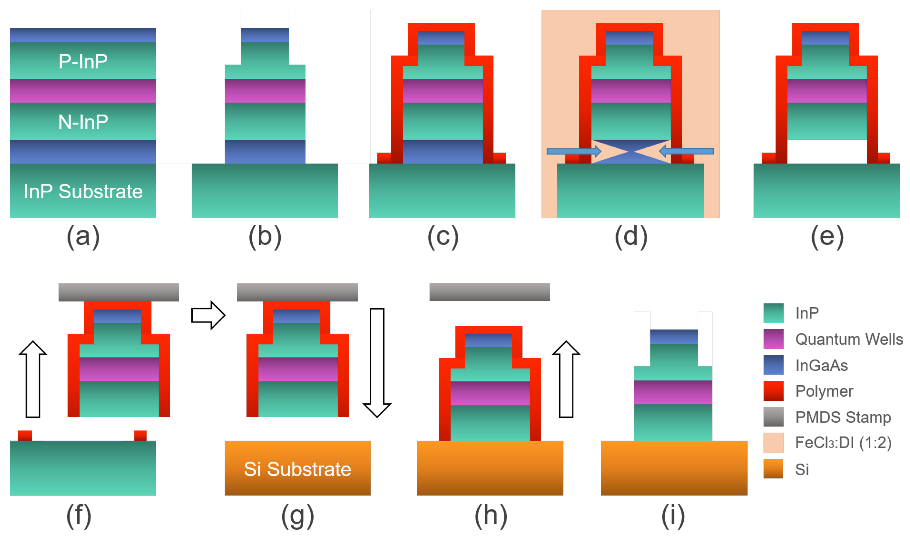
4.2. Micro-Transfer Printing

Through FCB many different state-of-the-art III–V-on-Si lasers have been demonstrated based on die-to-wafer bonding techniques, the problem of material wastage is still a concern, which is related to the millimeter-scale minimum die size for handling purposes. This introduces a limit on the density of possible device integration. One possible solution under investigation in recent years is Micro-transfer-printing (MTP) [54,55]. MTP presents itself as an alternative to FCB as an effective way to integrate III–V opto-electronic components onto a silicon photonic integrated circuit [56,57].
In MTP optical components are densely produced on their native III–V substrate which allows the minimization of waste of III–V material, providing cost savings to the process. The III–V epitaxial structure is grown with a thin sacrificial release layer which can be etched away at the completion of the III–V processing steps allowing the manipulation of micron-sized thin films devices on coupon structures, such that they can be printed in a massively parallel way to the designated target substrate such as Silicon and patterned Silicon on Insulator (SOI). The sacrificial release layer used in the case of InP-based epitaxy can be either InGaAs or InAlAs [58].
Devices or material coupons are patterned on the III–V source wafer and are covered with a photoresist encapsulation, with local openings to access the release layer. The release layer can then be selectively etched. This selective etching agent uses FeCl3:H2O for InP-based epitaxy [56]. Small polymer tether-like structures remain after the release etch to prevent immediate disconnection of the coupons from their native substrate. Using a polydimethylsiloxane (PDMS) stamp these coupons can then be individually or massively parallel lifted from the native substrate. Manipulation of the stamp’s impact parameters allows it to pick up the coupons and break the tethers holding the coupon to the substrate. These coupons can be subsequently “printed” on a Silicon target wafer with high alignment accuracy (+/−1.5 μ m 3 σ [59]) again through manipulation of the PDMS stamp. MTP has demonstrated successful lasers on Silicon [16,60]. The main process flow for micro-transfer printing is shown in Figure 4 [61].
Transfer printing offers a convenient method of integrating laser gain material on silicon. The usefulness of transfer printing does not end there however. Vanackere et al. demonstrates the successful transfer printing of a LN MZI achieving a modulation efficiency of V π L = 5.5 V·cm [62].

5. Creating Transfer Printable EAM Devices

With the growing improvements in micro-transfer printing (MTP) technology the options for Silicon compatible III–V modulators grows. To this end, the Integrated Photonics Group (IPG) at Tyndall National Institute have been developing a MTP-compatible III–V modulator for use in Silicon photonics. This modulator consists of a III–V laser and EAM to form an Externally Modulated Laser (EML). The benefit to transfer printing an EML compared to its individual components is the reduction in coupling losses due to the misalignment of separate components.
To monolithically integrate these two optical components a unique InP-based Multi-Quantum Well (MQW) epitaxy was designed for the fabrication of a monolithically integrated EML. The goal of this structure is to balance the MQW requirements of the laser, whose performance is optimal using a lower number of smaller quantum wells, typically 5, and the requirements of the EAM, whose performance is optimal using a higher number of wider quantum wells, typically >10. To determine the ideal balance point between these two structures simulations were completed to determine the effect the MQW structure on the performance of a Fabry Perot (FP) laser, shown in Figure 5. These simulations were completed in PICWAVE and HAROLD, software licensed from Photon Design. The effect of the MQW structure on the EAM was also simulated using software provided by the Integrated Photonics Group.
The material produced was then combined with a unique EAM pattern designed to minimize the parasitic capacitance typically found in lumped EAM devices. S11 measurements of the EAMs fabricated show a parasitic contact pad capacitance of 15 fF. The data from these S11 measurements was used to simulate the S21 performance of the EAM as shown in Figure 6 below. These measurements bode well for future prospects of high-speed Si-compatible EAMs. Further work continues on the optimization of device designs using this material, with a focus on BPSK and PAM-4 modulation.

6. Hybrid Silicon Modulators beyond III–V

EAMs have also been shown through the combination of germanium with silicon. Tensile strained germanium grown on silicon has been shown to enhance the Franz-Keldysh effect of germanium, causing it to behave more similarly to a direct bandgap material [63]. The Franz-Keldysh effect serves as a bulk material’s answer to the QCSE observed in quantum well materials. Both represent the change in optical absorption through the application of an external electric field to a material. Fujikata et al. showcases a GeSi EAM capable of operating in the C-band with a 56-Gbps NRZ and 56-Gbaud PAM4 high speed with 2.5-Vpp applied voltage [64].
More exotic materials have also been investigated with the intentions of creating an integrated silicon modulator. Sorianello et al. explores the usage of graphene-on-silicon modulators [65]. Graphene, a single-atom-thick layer of carbon atoms arranged in a hexagonal lattice, possesses many unique and valuable electronic properties. Graphene’s combination of zero-bandgap and ultra-broadband tunable optical absorption make it a prime candidate for usage in photonics. Thus far, single layer graphene (SLG) on silicon modulators with an on-off keying have shown modulation speeds up of 1, 10, and 20 Gb/s [66,67,68]. Dual layer graphene (DLG) on silicon modulators have also been demonstrated, thought the difficulty in depositing the second layer while leaving the first undamaged has led to few devices capable of operating in the GHz regime [69,70,71]. Sorianello demonstrates the first dual layer graphene on silicon EAM capable of operating at 50 Gb/s in [65].
Lihtium Niobate (LN) has also been a subject of interest in recent years due to its excellent electro-optic performance, owing to the Pockels effect [72]. LN modulators offer high-baud-rate multilevel signals well suited for long-haul links but are conventionally bulky and do not exhibit attractive modulation efficiency ( V π L > 10 V·cm) due to weak optical confinement. New techniques have been researched over the years, however, which use lithium-niobate membranes on insulator (LNOI) materials to create high confinement waveguides [73]. This discovery has facilitated an alternate use of lithium niobate through the hybrid integration of LN membranes onto silicon. Mercante et al. demonstrates a thin LiNbO3 layer on silicon and a novel RF tuning technique to achieve speeds from DC to 110 GHz [74]. Mingbo et al. has demonstrated a hybrid silicon-lithium-niobate MZM that uses vertical adiabatically coupled hybrid waveguides. This device has been shown to achieve on-off-keying modulation speeds of up to 100 Gb/s and PAM-4 speeds of 112 Gb/s [75].
Barium titanate has also been a thin film material of interest for monolithic integration with silicon due to its large Pockels coefficient even in thin film form [76]. Eltes et al. made use of this feature to fabricate an MZM with good modulation efficiency V π L = 0.2 V·cm capable of operating at a speed of 25 GHz with low power consuming tunability < 100 nW [77].

6.1. Plasmonics

In recent years, new modulators have been demonstrated utilizing plasmonics instead of photonics. In plasmonics, light strikes the interface between a metal and an insulator at a shallow angle, creating plasmons; waves of electron density that travel along the surface of the metal. Plasmons are capable of travelling along a waveguide that is narrower than the light that creates it. The high field confinement of plasmons is owed to a combination of the benefits of optical waves with the high localization of electronic waves, which can be exploited to develop novel plasmonic devices with footprints on the order of μ m 2 . Original studies of plasmonics limited themselves to noble metals such as silver and gold however their ability to contaminate some semiconductor materials can make them unattractive for CMOS integration. Alternative CMOS compatible metals have been subsequently identified to compensate for this shortcoming [78,79,80]. Modern plasmonics mainly focuses on aluminium [81], titanium nitride [82], and copper [83,84].
Kock et al. has demonstrated the monolithic integration of plasmonic MZMs on the silicon platform via a bipolar CMOS (BiCMOS) technology which has been shown to be capable of achieving high-speed data transmission, with symbol rates surpassing 100 GBd on a footprint of 29 × 6 μ m 2 [85]. Koch achieves this feat through the monolithic integration of a BiCMOS electronic-plasmonic transmitter. The electronic layer offers a BiCMOScircuit for 4:1 power multiplexing for simulating on-off keying to the plasmonic layer above which contains a compact, high bandwidth MZM. Hoessbacher et al. utilises organic layer plasmon assisted MZMs to achieve 100 Gbd non-return-to-zero (NRZ) operation and 60 Gbd PAM-4 operation [86]. The main shortcoming of plasmonics originates with ohmic losses due to the heat generated by electron movement. Haffner et al. showcase a device which proposes a method of overcoming this loss through a technique coined as “resonant switching”. Haffner et al. exhibit this technique to produce a plasmonic electro-optic ring modulator with low losses and operation over 100 GHz [87]. The field of plasmonics continues to bloom as a competitive candidate for silicon photonics in the regime of compact, high-speed communication technologies.

6.2. Epsilon-Near-Zero (ENZ) Modulators

Another approach of interest appearing under the umbrella of plasmonic research into electro-optic modulators takes aim at transparent conductive oxides (TCOs). TCOs have garnered increased research interest in recent years due to their unique electrical and optical properties [80,88,89]. TCOs act as wide-bandgap semiconductors with notable tunability of optical permittivity from its free carrier concentration [88]. The optical properties of TCOs can be varied from metal behaviour to dielectric behaviour via a gate voltage. In transition, the absolute permittivity of the material reaches a “near-zero” value, thus earning the moniker; Epsilon-near-zero (ENZ) [90]. Indium-Tin-Oxide (ITO) and Indium Oxide (IO) have been the most notable materials of study for this reason. Fast carrier dynamics, high absorption under bias and a large change in refractive index are some of ITOs useful properties for modulation [91,92,93].
The first high-speed demonstration of a compact ENZ EAM is accredited to Keeler et al. in 2017 [94]. The modulator shows a modulator 4 μ m in length with an extinction of 6 dB over a wavelength range of 1530–1590 nm. The modulator speed was tested up to 2.5 Gb/s. Gao et al. also demonstrate an ITO ENZ modulator with ultra high modulation strengths of 1.5 dB/ μ m [95]. The modulator demonstrates a uniform electro-optic modulation with 70 nm optical bandwidth from 1530–1600 nm at a dynamic modulation speed of 40 MHz.
Overall, the benefits of ENZ modulators are their ultra-small footprint due to their high absorption and their ultra-wide operation bandwidth however the speeds of these devices are lacking compared to their more established photonic counterparts.

7. Conclusions

In this paper we have analysed structures most commonly used in the fabrication of silicon modulators and the method behind their operation, the results of which are summarised in Table 1. Research continues to produce pure silicon devices which push the speeds and performance of modulators to new heights. We also explored the integration of silicon with III–V and other materials which allows the wealth of research performed on those materials to be married into the silicon photonics platform. Direct bonding methods and transfer printing are proving popular not just for the integration of modulators onto silicon, but also for integrating laser light sources, which is a highly desired feature in the silicon photonics suite. The authors of this paper explore the possibility of a monolithically integrated EML suitable for micro-transfer printing with the intention of bringing a monolithic optical switch onto the silicon platform. Currently the devices produced via the integration of III–V devices on silicon lag behind their pure silicon or pure III–V counterparts however research continues to show improvement on this front.
We also explore hybrids beyond III–V by looking at germanium, graphene, lithium niobate, and barium titanate. Herein, lithium niobate already shows impressive performance however the usage of graphene here is relatively new, and thus the performance of graphene-silicon modulators is particularly impressive in terms of performance and will likely continue to improve in coming years and the implementation of dual layer graphene matures and becomes more reliable. Finally we explored the blossoming fields of plasmonics and epsilon-near-zero modulators. Plasmonics continues to showcase excellently performing modulators and as the research continues, if the achievements noted in this paper can be combined then the field of plasmonics could become a primary competitor in the field of high speed communication technologies. ENZ devices are a relatively new form of modulator, with the first high speed ENZ EAM only appearing in 2017. Nevertheless their small footprint and high absorption will no doubt make them a subject of interest in the coming years.

Funding

This research was funded by Science Foundation Ireland (SFI) through the Irish Photonic Integration Centre (IPIC) under SFI-12/RC/2276_P2.

Institutional Review Board Statement

Not applicable.

Informed Consent Statement

Not applicable.

Data Availability Statement

No new data were created or analyzed in this study. Data sharing is not applicable to this article.

Conflicts of Interest

The authors declare no conflict of interest.

References

  1. Wang, X.; Weigel, P.; Zhao, J.; Ruesing, M.; Mookherjea, S. Achieving beyond-100-GHz large-signal modula-tion bandwidth in hybrid silicon photonics Mach Zehnder modulators using thin film lithium niobate. APL Photonics 2019, 4, 096101. [Google Scholar] [CrossRef] [Green Version]
  2. Bogaerts, W.; Taillaert, D.; Luyssaert, B.; Dumon, P.; Campenhout, J.; Bienstman, P.; Thourhout, D.; Baets, R.; Wiaux, V.; Beckx, S. Basic structures for photonic integrated circuits in Silicon-on-insulator. Opt. Express 2004, 12, 1583. [Google Scholar] [CrossRef] [PubMed]
  3. Luyssaert, B.; Vandersteegen, P.; Taillaert, D.; Dumon, P.; Bogaerts, W.; Bienstman, P.; Van Thourhout, D.; Wiaux, V.; Beckx, S.; Baets, R. A compact photonic horizontal spot-size converter realized in silicon-on-insulator. IEEE Photonics Technol. Lett. 2005, 17, 73–75. [Google Scholar] [CrossRef] [Green Version]
  4. Dumon, P.; Bogaerts, W.; Wiaux, V.; Wouters, J.; Beckx, S.; Van Campenhout, J.; Taillaert, D.; Luyssaert, B.; Bienstman, P.; Van Thourhout, D.; et al. Low-Loss SOI Photonic Wires and Ring Resonators Fabricated With Deep UV Lithography. IEEE Photonics Technol. Lett. 2004, 16, 1328–1330. [Google Scholar] [CrossRef] [Green Version]
  5. Doylend, J.K.; Knights, A.P. The evolution of silicon photonics as an enabling technology for optical interconnec-tion. Laser Photonics Rev. 2012, 6, 504–525. [Google Scholar] [CrossRef]
  6. Liu, A.; Jones, R.; Liao, L.; Samara-Rubio, D.; Rubin, D.; Cohen, O.; Nicolaescu, R.; Paniccia, M. A high-speed silicon optical modulator based on a metal-oxide-semiconductor capacitor. Nature 2004, 427, 615–618. [Google Scholar] [CrossRef] [PubMed]
  7. Marris-Morini, D.; Le Roux, X.; Vivien, L.; Cassan, E.; Pascal, D.; Halbwax, M.; Maine, S.; Laval, S.; Fédéli, J.M.; Damlencourt, J.F. Optical modulation by carrier depletion in a silicon PIN diode. Opt. Express 2006, 14, 10838–10843. [Google Scholar] [CrossRef] [PubMed]
  8. Xu, Q.; Schmidt, B.; Pradhan, S.; Lipson, M. Micrometrescale silicon electro-optic modulator. Nature 2005, 435, 325–327. [Google Scholar] [CrossRef] [PubMed]
  9. Green, W.M.J.; Rooks, M.J.; Sekaric, L.; Vlasov, Y.A. Ultracompact, low RF power, 10 Gb/s silicon Mach-Zehnder modulator. Opt. Express 2007, 15, 17106–17113. [Google Scholar] [CrossRef]
  10. Manipatruni, S.; Xu, Q.; Schmidt, B.; Shakya, J.; Lipson, M. High speed carrier injection 18 Gb/s silicon micro-ring electro-optic modulator. In Proceedings of the LEOS 2007-IEEE Lasers and Electro-Optics Society Annual Meeting Conference Proceedings Lasers and Electro-Optics Society, Lake Buena Vista, FL, USA, 21–25 October 2007; pp. 537–538. [Google Scholar]
  11. Liao, L.; Liu, A.; Rubin, D.; Basak, J.; Chetrit, Y.; Nguyen, H.; Cohen, R.; Izhaky, N.; Paniccia, M. 40 Gbit/s silicon optical modulator for highspeed applications. Electron. Lett. 2007, 43, 1196–1197. [Google Scholar] [CrossRef]
  12. Liu, A.; Liao, L.; Rubin, D.; Basak, J.; Chetrit, Y.; Nguyen, H.; Cohen, R.; Izhaky, N.; Paniccia, M. Recent development in a high-speed silicon optical modulator based on reverse-biased pn diode in a silicon waveguide. Semicond. Sci. Technol. 2008, 23, 064001. [Google Scholar] [CrossRef]
  13. Rosenberg, J.C.; Green, W.M.J.; Assefa, S.; Schow, C.L.; Rylyakov, A.V.; Gill, D.M.; Lee, B.G.; Jahnes, C.; Barwicz, T.; Shank, S.M.; et al. High-speed and low-power microring modulators for silicon photonics. In Proceedings of the IEEE Photonic Society 24th Annual Meeting, Arlington, VA, USA, 9–13 October 2011; pp. 256–257. [Google Scholar]
  14. Sun, J.; Kumar, R.; Sakib, M.; Driscoll, J.; Jayatilleka, H.; Rong, H. A 128 Gb/s PAM4 Silicon Microring Modulator With Integrated Thermo-Optic Resonance Tuning. J. Light. Technol. 2019, 37, 110–115. [Google Scholar] [CrossRef]
  15. Bogaerts, W.; De Heyn, P.; Van Vaerenbergh, T.; De Vos, K.; Kumar Selvaraja, S.; Claes, T.; Dumon, P.; Bienstman, P.; Van Thourhout, D.; Baets, R. Silicon microring resonators. Laser Photonics Rev. 2011, 6, 47–73. [Google Scholar] [CrossRef]
  16. Soref, R.; Bennett, B. Electrooptical effects in silicon. IEEE J. Quantum Electron. 1987, 23, 123–129. [Google Scholar] [CrossRef] [Green Version]
  17. Timurdogan, E.; Sorace-Agaskar, C.M.; Sun, J.; Hosseini, E.S.; Biberman, A.; Watts, M.R. An ultralow power athermal silicon modulator. Nat. Commun. 2014, 5, 4008. [Google Scholar] [CrossRef] [PubMed] [Green Version]
  18. Preston, K.; Sherwood-Droz, N.; Levy, J.S.; Lipson, M. Performance guidelines for WDM interconnects based on silicon microring resonators. In Proceedings of the CLEO: 2011-Laser Science to Photonic Applications, Baltimore, MD, USA, 1–6 May 2011; pp. 1–2. [Google Scholar]
  19. Dinu, M.; Quochi, F.; Garcia, H. Third-order nonlinearities in silicon at telecom wavelengths. Appl. Phys. Lett. 2003, 82, 2954–2956. [Google Scholar] [CrossRef]
  20. Almeida, V.R.; Lipson, M. Optical bistability on a silicon chip. Opt. Lett. 2004, 29, 2387–2389. [Google Scholar] [CrossRef] [PubMed]
  21. Xu, Q.; Lipson, M. Carrier-induced optical bistability in silicon ring resonators. Opt. Lett. 2006, 31, 341–343. [Google Scholar] [CrossRef] [Green Version]
  22. Johnson, T.J.; Borselli, M.; Painter, O. Self-induced optical modulation of the transmission through a high-Q silicon microdisk resonator. Opt. Express 2006, 14, 817–831. [Google Scholar] [CrossRef] [PubMed]
  23. Koyama, F.; Iga, K. Frequency chirping in external modulators. J. Light. Technol. 1988, 6, 87–93. [Google Scholar] [CrossRef]
  24. Gnauck, A.H.; Winzer, P.J. Optical phase-shift-keyed transmission. J. Light. Technol. 2005, 23, 115–130. [Google Scholar] [CrossRef]
  25. Winzer, P.J.; Essiambre, R. Advanced Optical Modulation Formats. Proc. IEEE 2006, 94, 952–985. [Google Scholar] [CrossRef]
  26. Kikuchi, K. Coherent transmission systems. In Proceedings of the 2008 34th European Conference on Optical Communication, Brussels, Belgium, 21–25 September 2008; pp. 1–39. [Google Scholar] [CrossRef]
  27. Reed, G.T.; Mashanovich, G.; Gardes, F.Y.; Thomson, D.J. Silicon optical modulators. Nature Photonics 2010, 4, 518–526. [Google Scholar] [CrossRef] [Green Version]
  28. Liow, T.Y.; Ang, K.W.; Fang, Q.; Song, J.F.; Xiong, Y.Z.; Yu, M.B.; Lo, G.Q.; Kwong, D.L. Silicon Modulators and Germanium Photodetectors on SOI: Monolithic Integration, Compatibility, and Performance Optimization. IEEE J. Sel. Top. Quantum Electron. 2010, 16, 307–315. [Google Scholar] [CrossRef]
  29. Damas, P.; Le Roux, X.; Le Bourdais, D.; Cassan, E.; Marris-Morini, D.; Izard, N.; Maroutian, T.; Lecoeur, P.; Vivien, L. Pockels effect study in Strained Silicon Mach-Zenhder Interferometer. In Proceedings of the 11th International Conference on Group IV Photonics (GFP), Paris, France, 27–29 August 2014; pp. 243–244. [Google Scholar] [CrossRef]
  30. Reed, G.T.; Mashanovich, G.Z.; Gardes, F.Y.; Nedeljkovic, M.; Hu, Y.; Thomson, D.J.; Li, K.; Wilson, P.R.; Chen, S.W.; Hsu, S.S. Recent breakthroughs in carrier depletion based silicon optical modulators. Nanophotonics 2014, 3, 229–245. [Google Scholar] [CrossRef] [Green Version]
  31. Webster, M.; Gothoskar, P.; Patel, V.; Piede, D.; Anderson, S.; Tummidi, R.; Adams, D.; Appel, C.; Metz, P.; Sunder, S.; et al. An efficient MOS-capacitor based silicon modulator and CMOS drivers for optical transmitters. In Proceedings of the 11th International Conference on Group IV Photonics (GFP), Paris, France, 27–29 August 2014; pp. 1–2. [Google Scholar] [CrossRef]
  32. Reed, G.; Thomson, D.; Gardes, F.; Hu, Y.; Fedeli, J.; Mashanovich, G. High-speed carrier-depletion silicon Mach-Zehnder optical modulators with lateral PN junctions. Front. Phys. 2014, 2, 77. [Google Scholar] [CrossRef] [Green Version]
  33. Xiao, X.; Xu, H.; Li, X.; Li, Z.; Chu, T.; Yu, Y.; Yu, J. High-speed, low-loss silicon Mach–Zehnder modulators with doping optimization. Opt. Express 2013, 21, 4116–4125. [Google Scholar] [CrossRef] [PubMed]
  34. Ackermann, D.A.; Johnson, J.E.; Ketelsen, L.J.P.; Eng, L.E.; Kiely, P.A.; Mason, T.G.B. Telecommunication lasers. In Optical Fiber Telecommunications IV; Kaminow, I., Li, T., Eds.; Academic Press: New York, NY, USA, 2002; pp. 587–665. [Google Scholar]
  35. Jeong, U.; Lee, D.H.; Lee, K.; Park, J.H. Monolithic 1 × 8 DWDM Silicon Optical Transmitter Using an Arrayed-Waveguide Grating and Electro-Absorption Modulators for Switch Fabrics in Intra-Data-Center Interconnects. Micromachines 2020, 11, 991. [Google Scholar] [CrossRef]
  36. Li, Q.; Ho, C.P.; Takagi, S.; Takenaka, M. Efficient optical modulator by reverse-biased III–V/ Si hybrid MOS capacitor based on FK effect and carrier depletion. In Proceedings of the 2019 Optical Fiber Communications Conference and Exhibition (OFC), San Diego, CA, USA, 3–7 March 2019. [Google Scholar]
  37. Li, Q.; Ho, C.P.; Takagi, S.; Takenaka, M. Optical phase modulators based on reverse-biased III–V/Si hybrid metal-oxide-semiconductor capacitors. IEEE Photonics Technol. Lett. 2020, 32, 345–348. [Google Scholar] [CrossRef]
  38. Li, Q.; Ho, C.; Takagi, S.; Takenaka, M. Si racetrack modulator with III–V/Si hybrid MOS optical phase shifter. In Proceedings of the 45th European Conference on Optical Communication (ECOC 2019), Dublin, Ireland, 22–26 September 2019. [Google Scholar]
  39. Ohno, S.; Li, Q.; Sekine, N.; Fujikata, J.; Noguchi, M.; Takahashi, S.; Toprasertpong, K.; Takagi, S.; Takenaka, M. Taper-less III–V/Si hybrid MOS optical phase shifter using ultrathin InP membrane. In Proceedings of the Optical Fiber Communication Conference, San Diego, CA, USA, 8–12 March 2020. [Google Scholar]
  40. Tang, Y.; Peters, J.D.; Bowers, J.E. Over 67 GHz bandwidth hybrid silicon electro-absorption modulator with asymmetric segmented electrode for 1.3 μm transmission. Opt. Express 2012, 20, 11529–11535. [Google Scholar] [CrossRef] [Green Version]
  41. Tang, Y.; Chen, H.W.; Jain, S.; Peters, J.D.; Westergren, U.; Bowers, J.E. 50 Gb/s hybrid silicon traveling-wave electro-absorption modulator. Opt. Express 2011, 19, 5811–5816. [Google Scholar] [CrossRef] [PubMed]
  42. Bruns, J.; Mitze, T.; Zimmermann, L.; Voigt, K.; Schnarrenberger, M.; Petermann, K. An optical board approach based on SOI (silicon-on-insulator). In Proceedings of the 9th International Conference on Transparent Optical Networks (ICTON 2007), Rome, Italy, 1–5 July 2007; pp. 179–182. [Google Scholar]
  43. Roelkens, G.; Brouckaert, J.; Thourhout, D.V.; Baets, R.; Notzel, R.; Smit, M. Adhesive bonding of InP/InGaAsP dies to processed silicon-on-insulator wafers using DVS-bis-benzocyclobutene. J. Electrochem. Soc. 2006, 153, G1015–G1019. [Google Scholar] [CrossRef] [Green Version]
  44. Soganci, I.; La Porta, A.; Offrein, B. Flip-chip optical couplers with scalable I/O count for silicon photonics. Opt. Express 2013, 21, 16075. [Google Scholar] [CrossRef] [PubMed]
  45. Shu, J.; Qiu, C.; Zhang, X.; Xu, Q. Efficient coupler between chip-level and board-level optical waveguides. Opt. Lett. 2011, 36, 3614–3616. [Google Scholar] [CrossRef] [PubMed] [Green Version]
  46. Fonstad, C.G.; Rumpler, J.J.; Barkley, E.R.; Perkins, J.M.; Famenini, S. Recess integration of microcleaved laser diode platelets with dielectric waveguides on silicon-art. no. 69090O. In Proceedings of the Conference on Novel inPlane Semiconductor Lasers VII, San Jose, CA, USA, 19–24 January 2008; p. O9090. [Google Scholar]
  47. Jokerst, N.; Royal, M.; Palit, S.; Luan, L.; Dhar, S.; Tyler, T. Chip scale integrated microresonator sensing systems. J. Biophotonics 2009, 2, 212–226. [Google Scholar] [CrossRef] [PubMed]
  48. Roelkens, G.; Van Campenhout, J.; Brouckaert, J.; Van Thourhout, D.; Baets, R.; Romeo, P.; Regreny, P.; Kazmierczak, A.; Seassal, C.; Letartre, X. III–V/Si photonics by die-to-wafer bonding. Mater. Today 2007, 10, 36–43. [Google Scholar] [CrossRef]
  49. Niklaus, F.; Stemme, G.; Lu, J. and Gutmann, R. Adhesive wafer bonding. J. Appl. Phys. 2006, 99, 031101. [Google Scholar] [CrossRef]
  50. Tong, Q.-Y.; Gösele, U. Semiconductor Wafer Bonding; Wiley-VCH: Berlin, Germany, 1999. [Google Scholar]
  51. Roelkens, G.; Abassi, A.; Cardile, P.; Dave, U.; de Groote, A.; de Koninck, Y.; Dhoore, S.; Fu, X.; Gassenq, A.; Hattasan, N. III–V-on-Silicon Photonic Devices for Op-tical Communication and Sensing. Photonics 2015, 2, 969–1004. [Google Scholar] [CrossRef] [Green Version]
  52. Liang, D.; Roelkens, G.; Baets, R.; Bowers, J. Hybrid Integrated Platforms for Silicon Photonics. Materials 2010, 3, 1782–1802. [Google Scholar] [CrossRef] [Green Version]
  53. Han, J.; Takenaka, M.; Takagi, S. Extremely high modulation efficiency III–V/si hybrid mos optical modulator fabricated by direct wafer bonding. In Proceedings of the 2016 IEEE International Electron Devices Meeting (IEDM), San Francisco, CA, USA, 3–7 December 2016; pp. 25.5.1–25.5.4. [Google Scholar] [CrossRef]
  54. Zhang, J.; Haq, B.; O’Callaghan, J.; Gocalinska, A.; Pelucchi, E.; Trindade, A.; Corbett, B.; Morthier, G.; Roelkens, G. Transfer-printing-based integration of a III–V-on-silicon distributed feedback laser. Opt. Express 2018, 26, 8821–8830. [Google Scholar] [CrossRef]
  55. De Groote, A.; Cardile, P.; Subramanian, A.; Fecioru, A.; Bower, C.; Delbeke, D.; Baets, R. and Roelkens, G. Transfer-printing-based integration of single-mode waveguide-coupled III–V-on-silicon broadband light emitters. Opt. Express 2016, 24, 13754–13762. [Google Scholar] [CrossRef] [PubMed] [Green Version]
  56. Zhang, J.; Groote, A.D.; Abbasi, A.; Loi, R.; O’Callaghan, J.; Corbett, B.; Trindade, A.J.; Bower, C.A.; Roelkens, G. Sili-con photonics fiber-to-the-home transceiver array based on transfer-printing-based integration of III–V photodetectors. Opt. Express 2017, 25, 14290–14299. [Google Scholar] [CrossRef] [PubMed] [Green Version]
  57. O’Callaghan, J.; Loi, R.; Mura, E.E.; Roycroft, B.; Trindade, A.J.; Thomas, K.; Gocalinska, A.; Pelucchi, E.; Zhang, J.; Roelkens, R.; et al. Comparison of InGaAs and InAlAs sacrificial layers for release of InP-based de-vices. Opt. Express 2017, 7, 4408–4414. [Google Scholar] [CrossRef] [Green Version]
  58. Han, J.H.; Boeuf, F.; Fujikata, J.; Takahashi, S.; Takagi, S.; Takenaka, M. Efficient low-loss InGaAsP/Si hybrid MOS optical modulator. Nat. Photonics 2017, 11, 486–490. [Google Scholar] [CrossRef]
  59. Hiraki, T.; Aihara, T.; Hasebe, K.; Takeda, K.; Fujii, T.; Kakitsuka, T.; Tsuchizawa, T.; Fukuda, H.; Matsuo, S. Heterogeneously integrated III–V/Si MOS capacitor Mach–Zehnder modulator. Nat. Photonics 2017, 11, 482–485. [Google Scholar] [CrossRef]
  60. Haq, B.; Rahimi Vaskasi, J.; Zhang, J.; Gocalinska, A.; Pelucchi, E.; Corbett, B.; Roelkens, G. Mi-cro-transfer-printed III–V-on-silicon C-band distributed feedback lasers. Opt. Express 2020, 28, 32793. [Google Scholar] [CrossRef] [PubMed]
  61. Loi, R.; O’Callaghan, J.; Roycroft, B.; Robert, C.; Fecioru, A.; Trindade, A.; Gocalinska, A.; Pelucchi, E.; Bower, C.; Corbett, B. Transfer Printing of AlGaInAs/InP Etched Facet Lasers to Si Substrates. IEEE Photonics J. 2016, 8, 1–10. [Google Scholar] [CrossRef]
  62. Vanackere, T.; Billet, M.; de Beeck, C.O.; Poelman, S.; Roelkens, G.; Clemmen, S.; Kuyken, B. Micro-Transfer Printing of Lithium Niobate on Silicon Nitride. In Proceedings of the 2020 European Conference on Optical Communications (ECOC), Brussels, Belgium, 6–10 December 2020. [Google Scholar]
  63. Liu, J.; Beals, M.; Pomerene, A.; Bernardis, S.; Sun, R.; Cheng, J.; Kimerling, L.; Michel, J. Wave-guide-integrated, ultralow-energy GeSi electro-absorption modulators. Nat. Photonics 2008, 2, 433–437. [Google Scholar] [CrossRef]
  64. Fujikata, J.; Noguchi, M.; Kawashita, K.; Katamawari, R.; Takahashi, S.; Nishimura, M.; Ono, H.; Shimura, D.; Takahashi, H.; Yaegashi, H.; et al. High-speed Ge/Si electro-absorption optical modu-lator in C-band operation wavelengths. Opt. Express 2020, 28, 33123. [Google Scholar] [CrossRef] [PubMed]
  65. Sorianello, V.; Contestabile, G.; Romagnoli, M. Graphene on Silicon Modulators. J. Light. Technol. 2020, 38, 2782–2789. [Google Scholar] [CrossRef] [Green Version]
  66. Liu, M.; Yin, X.; Ulin-Avila, E.; Geng, B.; Zentgraf, T.; Ju, L.; Wang, F.; Zhang, X. A graphene-based broadband optical modulator. Nature 2011, 474, 64–67. [Google Scholar] [CrossRef] [PubMed]
  67. Hu, Y.; Pantouvaki, M.; Van Campenhout, J.; Brems, S.; Asselberghs, I.; Huyghebaert, C.; Absil, P.; Van Thourhout, D. Broadband 10 Gb/s operation of graphene electroabsorption modulator on silicon. Laser Photonics Rev. 2016, 10, 307–316. [Google Scholar] [CrossRef] [Green Version]
  68. Alessri, C.; Asselberghs, I.; Ban, Y.; Brems, S.; Huyghebaert, C.; Van Campenhout, J.; Van Thourhout, D.; Pantouvaki, M. Broadband 20 Gbit/s Graphene-si Electro-Absorption Modulator. In Proceedings of the 2018 European Conference on Optical Communication (ECOC), Rome, Italy, 23–27 September 2018. [Google Scholar]
  69. Liu, M.; Yin, X.; Zhang, X. Double-layer Graphene optical modulator. Nano Lett. 2012, 12, 1482–1485. [Google Scholar] [CrossRef] [PubMed]
  70. Phare, C.T.; Lee, Y.D.; Cardenas, J.; Lipson, M. Graphene electro-optic modulator with 30 GHz bandwidth. Nat. Photonics 2015, 9, 511–514. [Google Scholar] [CrossRef]
  71. Dalir, H.; Xia, Y.; Wang, Y.; Zhang, X. Athermal broadband grapheneoptical modulator with 35 GHz speed. ACS Photon. 2016, 3, 1564–1568. [Google Scholar] [CrossRef]
  72. Chen, A. Broadband Optical Modulators: Science, Technology, and Applications; CRC Press: Boca Raton, FL, USA, 2011. [Google Scholar]
  73. Boes, A.; Corcoran, B.; Chang, L.; Bowers, J.; Mitchell, A. Status and potential of lithium niobate on insulator (LNOI) for photonic integrated circuits. Laser Photon. Rev. 2018, 12, 1700256. [Google Scholar] [CrossRef]
  74. Mercante, A.; Yao, P.; Shi, S.; Schneider, G.; Murakowski, J.; Prather, D. 110 GHz CMOS compatible thin film LiNbO3 modulator on silicon. Opt. Express 2016, 24, 15590. [Google Scholar] [CrossRef] [PubMed]
  75. He, M.; Xu, M.; Ren, Y.; Jian, J.; Ruan, Z.; Xu, Y.; Gao, S.; Sun, S.; Wen, X.; Zhou, L.; et al. High-performance hybrid silicon and lithium niobate Mach–Zehnder modulators for 100 Gbit/s and beyond. Nat. Photonics 2019, 13, 359–364. [Google Scholar] [CrossRef]
  76. Abel, S.; Eltes, F.; Ortmann, J.E.; Messner, A.; Castera, P.; Wagner, T.; Urbonas, D.; Rosa, A.; Gutierrez, A.M.; Tulli, D.; et al. Large Pockels Effect in Micro- and Nanostructured Barium Titanate Integrated on Silicon. Nat. Mater. 2019, 18, 42–47. [Google Scholar] [CrossRef] [PubMed]
  77. Eltes, F.; Mai, C.; Caimi, D.; Kroh, M.; Popoff, Y.; Winzer, G.; Petousi, D.; Lischke, S.; Ortmann, J.; Czornomaz, L. A BaTiO3-Based Electro-Optic Pockels Modulator Monolithically Inte-grated on an Advanced Silicon Photonics Platform. J. Light. Technol. 2019, 37, 1456–1462. [Google Scholar] [CrossRef] [Green Version]
  78. West, P.R.; Ishii, S.; Naik, G.V.; Emani, N.K.; Shalaev, V.M.; Boltasseva, A. Searching for better plasmonic materials. Laser Photon. Rev. 2010, 4, 795–808. [Google Scholar] [CrossRef] [Green Version]
  79. Boltasseva, A.; Atwater, H.A. Low-loss plasmonics metamaterials. Science 2011, 331, 290–291. [Google Scholar] [CrossRef]
  80. Naik, G.V.; Shalaev, V.M.; Boltasseva, A. Alternative plasmonic materials: Beyond gold and silver. Adv. Mater. 2013, 25, 3264–3294. [Google Scholar] [CrossRef] [PubMed]
  81. Zektzer, R.; Desiatov, B.; Mazurski, N.; Bozhevolnyi, S.I.; Levy, U. Experimental demonstration of cmoscompatible long-range dielectric loaded surface plasmon waveguides (lr-dlsppws). Opt. Express 2014, 22, 22009–22017. [Google Scholar] [CrossRef] [PubMed]
  82. Kinsey, N.; Ferrera, G.V.; Naik, M.; Babicheva, V.E.; Shalaev, V.M.; Boltasseva, A. Experimental demonstration of titanium nitride interconnects. Opt. Express 2014, 22, 12238–12247. [Google Scholar] [CrossRef] [PubMed] [Green Version]
  83. Delacour, C.; Blaize, S.; Grosse, P.; Fedeli, J.-M.; Bruyant, A.; Salas-Montiel, R.; Lerondel, G.; Chelnokov, A. Efficient directional coupling between silicon and copper plasmonic nanoslot waveguides: Toward metal-oxidesilicon nanophotonics. Nano Lett. 2010, 10, 2922–2926. [Google Scholar] [CrossRef] [PubMed]
  84. Fedyanin, D.Y.; Yakubovsky, D.I.; Kirtaev, R.V.; Volkov, V.S. Ultralow-loss cmos copper plasmonic waveguides. Nano Lett. 2016, 16, 362–366. [Google Scholar] [CrossRef] [PubMed]
  85. Koch, U.; Uhl, C.; Hettrich, H.; Fedoryshyn, Y.; Hoessbacher, C.; Heni, W.; Baeuerle, B.; Bitachon, B.; Josten, A.; Ayata, M.; et al. A monolithic bipolar CMOS electronic–plasmonic high-speed transmitter. Nat. Electron. 2020, 3, 338–345. [Google Scholar] [CrossRef]
  86. Hoessbacher, C.; Josten, A.; Baeuerle, B.; Fedoryshyn, Y.; Hettrich, H.; Salamin, Y.; Heni, W.; Haffner, C.; Kaiser, C.; Schmid, R.; et al. Plasmonic modulator with >170 GHz bandwidth demonstrated at 100 GBd NRZ. Opt. Express 2017, 25, 1762–1768. [Google Scholar] [CrossRef] [PubMed]
  87. Haffner, C.; Chelladurai, D.; Fedoryshyn, Y.; Josten, A.; Baeuerle, B.; Heni, W.; Watanabe, T.; Cui, T.; Cheng, B.; Saha, S.; et al. Low-loss plasmon-assisted electro-optic modulator. Nature 2018, 556, 483–486. [Google Scholar] [CrossRef] [PubMed]
  88. Naik, G.V.; Kim, J.; Boltasseva, A. Oxides and nitrides as alternative plasmonic materials in the optical range [invited]. Opt. Mater. Express 2011, 1, 1090–1099. [Google Scholar] [CrossRef] [Green Version]
  89. Ma, Z.; Li, Z.; Liu, K.; Ye, C.; Sorger, V.J. Indium-tin-oxide for high-performance electro-optic modulation. Nanophotonics 2015, 4, 198–213. [Google Scholar] [CrossRef]
  90. Liberal, I.; Engheta, N. Near-zero refractive index photonics. Nat. Photonics 2017, 11, 149–158. [Google Scholar] [CrossRef]
  91. Kuang, Y.; Liu, Y.; Tian, L.; Han, W.; Li, Z. A Dual-Slot Electro-Optic Modulator Based on an Epsilon-Near-Zero Oxide. IEEE Photonics J. 2019, 11, 1–12. [Google Scholar] [CrossRef]
  92. Kim, J.; Kim, J. Silicon electro-optic modulator based on an ITO-integrated tunable directional coupler. J. Phys. Appl. Phys. 2016, 49, 075101. [Google Scholar] [CrossRef]
  93. Vasudev, A.; Kang, J.; Park, J.; Liu, X.; Brongersma, M. Electro-optical modulation of a silicon waveguide with an “epsilon-near-zero” material. Opt. Express 2013, 21, 26387. [Google Scholar] [CrossRef] [PubMed]
  94. Keeler, G.A.; Geib, K.M.; Serkland, D.K.; Parameswaran, S.; Luk, T.S.; Griñe, A.J.; Ihlefeld, J.; Campione, S.; Wendt, J.R. Multi-gigabit operation of a compact, broadband modulator based on ENZ confinement in indium oxide. In Proceedings of the 2017 Optical Fiber Communications Conference and Exhibition (OFC), Los Angeles, CA, USA, 19–23 March 2017. [Google Scholar]
  95. Gao, Q.; Li, E.; Wang, A. Ultra-compact and broadband electro-absorption modulator using an epsilon-near-zero conductive oxide. Photonics Res. 2018, 6, 277. [Google Scholar] [CrossRef]
Figure 1. Ring modulator schematic with (a) Top down view showing the ring and the coupling waveguide (b) the diode embedded in the cross section (c) The effect biasing has on the transmission of the ring.
Photonics 09 00040 g001
Figure 2. (a) Schematic of Si racetrack resonator with III–V/Si hybrid MOS optical phase shifter. (b) Numerically calculated transmission of a MZI modulator and a racetrack resonator.
Photonics 09 00040 g002
Figure 3. III–V on Silicon bonding process flow.
Photonics 09 00040 g003
Figure 4. Devices are fabricated on an InP wafer including an InGaAs release layer at the bottom of the epitaxial structure (a,b). An anchor system made of polymer (resist) keeps the devices in place (c) during the undercut while allowing the etchant to penetrate underneath the mesas through some openings (d,e). Finally, the devices are picked up (f) and transfer-printed onto the new substrate using a Polydimethylsiloxane (PDMS) stamp (gi).
Photonics 09 00040 g004
Figure 5. Quantum well width and number vs. (a) Fabry Perót (FP) Laser Threshold (b) FP slope efficiency. (c) Quantum well width vs. Extinction Ratio (ER) divided by Insertion Loss (IL) (d) Quantum well number vs. ER.
Photonics 09 00040 g005
Figure 6. Simulated S21 measurements extracted from experimental S11 measurements of EAM devices with length 50 μ m and width 25 μ m with impedance (a) 50 Ω (b) 25 Ω .
Photonics 09 00040 g006
Table 1. A comparison table of noted figures of merit for the various state of the art devices researched for this paper. NA indicates that the desired quantity was not made available. * indicates the the value was simulated but not yet experimentally verified.
Modulator TypeSpeed Achieved (Gb/s)Bandwidth (GHz)Footprint ( μ m 2 )Loss (dB)Figure of Merit
LiN MZM [1]20>100NA7.7 dB/cmNA
Si MZM [6]11>25006.7 V π · L = ∼8 V·cm
Si Phase Modulator [7]NANANANA V π · L = 3.1 V·cm
Si MRM [8]1.5NA>1154NA
Si MRM [10]18NA>450NANA
Si MZM [11]4030NA<4 V π · L = <4 V·cm
Si MZM [12]4030>NA∼7 V π · L = ∼4 V·cm
Si MRM [13]30NA>300NA V π · L = ∼0.65 V·cm
Si MRM [14]12850>3002.9–4.2 V π · L = 0.52 V·cm
Si MRM [17]25–4435>1829 dB/cmNA
Si MZM [31]28–40NANA6.5 dB/mm V π · L = 2 V·mm
Si MZM [32]52NANA51.4–1.9 V/cm
Si MZM [33]6027.7NA3.5 V π · L = 2 V·cm
Si EAM [35]4 GHz1542–1558 nmNA51NA
III–V Si MOS [36]NANANANA V π · L = 0.11 V·cm
III–V Si MOS [37]NA100 expectedNA28 dB/cm V π · L = 0.12–0.17 V·cm
III–V Si MRM [38]38 GHz50NANA V π · L = 0.059–0.064 V·cm
III–V Si MZM [39]NANANANA V π · L = 0.1 V·cm
III–V Si EAM [40]5074NA4.9NA
III–V Si EAM [41]5042NA>15NA
III–V Si MZM [53]NANANANA V π · L = 0.047 V·cm
LN Si MZM [62]NANA240,0007 V π · L = 5.5 V·cm
GeSi EAM [63]10 GHz1539–1553 nm30–200>5ER/IL = 10/3.7
GeSi EAM [64]56NA∼4004ER/IL = 0.1–0.8
DLG on Si [65]50NANA20ER/IL = 3/20
SLG on Si [66]1.2 GHz1.35–1.6 μ m25NANA
SLG on Si [67]10NA5002.8ER/IL = 3.5/2.8
SLG on Si [68]2070 nmNA7.7ER/IL = 4.4/7.7
DLG on Si [69]1 GHzNA>80NANA
DLG on Si [70]22NANANA f m a x D d B / ( V s w i n g I L d B ) = 3.75 GHz/V
DLG on Si [71]35 GHz1500–1640 nm180.9ER/IL = 2/0.9
L i N b 0 3 on Si [74]110 GHzNANA15DC- V π = 9.4 V
LN MZM [75]100–112 * expectedNANA2.5 V π = 5.1 V
BTO MZM [77]25NANA5.8 dB/cm V π · L = 0.2 V·cm
Plasmonic MZM [85]100NANA27ER/IL = 10/27
Plasmonic MZM [86]100NANA8NA
Plasmonic Ring [87]72NANA2.5ER/IL = 10/2.5
ENZ EAM [94]2.570 nmNANANA
ITO ENZ [95]40 MHz70 nmNANANA
Publisher’s Note: MDPI stays neutral with regard to jurisdictional claims in published maps and institutional affiliations.

