3. Results and Discussion
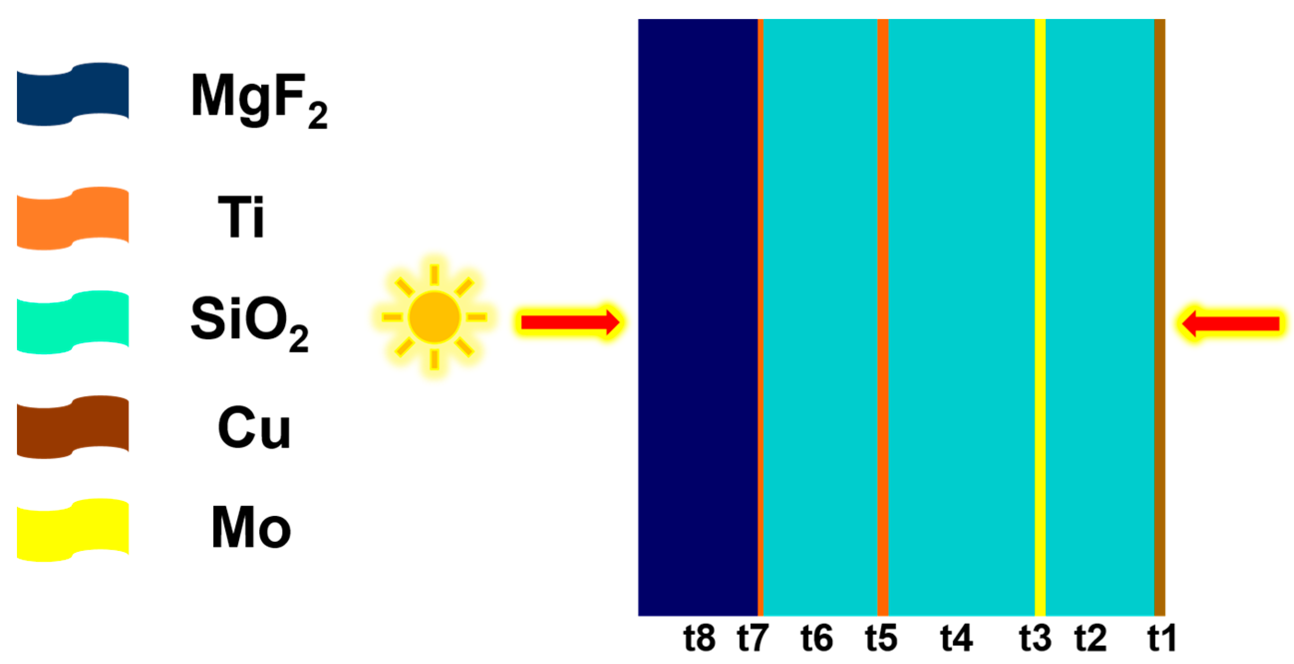
To verify the optimized thickness of the materials in each layer in our proposed structure, we conducted experiments wherein we varied the thickness of each layer’s material individually, while keeping the thicknesses of other layers constant.
Figure 2 (for t8 MgF
2 layer) and
Figure 3 (for t7–t3 layers) demonstrate the changes in absorptivity for the different layers of the designed absorber when the thickness of each layer’s material was altered. This method serves as the basis for determining the optimal parameters of the investigated absorber, which exhibits ultra-broadband absorption and high absorptivity.
Figure 2 and
Figure 3 depict the changes in the absorptivity of the designed absorber that result from altering the thickness of a single layer while keeping the other layers unchanged, as presented in
Figure 1. The optimizations of thicknesses were performed across a wavelength range of 280 to 3000 nm. The results presented in
Figure 2 and
Figure 3 clearly indicate significant variations in absorptivity based on the thicknesses of different layers, demonstrating the notable influence of layer thickness on the numerical outcome of absorptivity.
The absorption spectra of the absorber being studied were numerically simulated to demonstrate the anti-reflection effect of the MgF
2 layer. Two scenarios were considered: one without the MgF
2 layer (represented by the 0 nm curve), and the other with varying thicknesses of the MgF
2 layer (ranging from 90 to 120 nm). The simulations were conducted under normal incident light. The results, as depicted in
Figure 2, clearly indicate that the absorber without the MgF
2 layer exhibited an apparent absorption peak at 460 nm and two unapparent absorption peaks at 755 and 1520 nm. Additionally, the absorptivity of the absorber exceeded 90.0% within the wavelength ranges of 425–945 nm and 1075–1875 nm, and the maximum absorptivity achieved an impressive value of 98.1% at 460 nm. However, the results shown in
Figure 3 clearly illustrate that the absorber with the anti-reflection MgF
2 layer exhibits significantly higher absorptivity compared to the absorber without the anti-reflection MgF
2 layer across the entire absorption spectrum.
As the thicknesses of MgF2 layer were 90, 100, 110, and 120 nm, the ranges in which the absorptivity of the investigated absorber exceeded 90.0% were 410–2220 nm, 410–2250 nm, 410–2280 nm, and 415–2310 nm, and the average absorptivities within these ranges were 96.1%, 96.6%, 97.0%, and 96.8%, respectively. The graph additionally indicates the existence of a prominent absorption peak at 430 nm. Furthermore, when the thickness of the MgF2 layer was set to 110 nm, three relatively less pronounced absorption peaks were observed at approximately 665, 880, and 150 nm. Notably, these three less prominent absorption peaks demonstrated a redshift as the thickness of the MgF2 layer increased, which suggests that these absorption peaks’ locations are caused by the localized surface plasmon resonance (LSPR); this will be explained in the next paragraph. Hence, the observation of redshift in the three less prominent absorption peaks suggests that their peak wavelengths shifted towards longer wavelengths as the thickness of the MgF2 layer was increased. This phenomenon provides valuable insights into the interaction between the MgF2 layer thickness and the absorber’s spectral response.
There are two main types of surface plasmon resonance (SPR): LSPR and propagating surface plasmon resonance (PSPR). The position of the LSPR peak depends on the local refractive index and the surrounding medium. The presence of a dielectric film in proximity to metal nanoparticles has a notable impact on the LSPR characteristics. Specifically, the thickness of the dielectric film plays a critical role in determining the wavelength at which LSPR occurs. As the thickness of the film varies, it alters the refractive index affecting the plasmonic nanoparticles, thereby inducing a shift in the LSPR peak. When a dielectric film is placed on or near metal nanoparticles, the wavelength of LSPR generally undergoes a redshift (longer wavelength) or blueshift (shorter wavelength) as the film thickness increases. It is worth noting that the specific relationship between LSPR and dielectric film thickness is intricate, and influenced by various factors. The nature of the shift depends on the refractive index of the dielectric material and its proximity to the nanoparticles. Generally, an increase in film thickness tends to lead to a redshift in the LSPR wavelength. After employing MgF2 as the leftmost layer, noticeable redshift phenomena in absorption peaks become apparent as the subsequent thickness increases. These findings substantiate the versatility of MgF2, which can serve not only as an antireflection layer, but also bestows distinct LSPR characteristics upon the entire multilayer structure.
Notably, the absorptivity within the range of 600–1030 nm exceeded 99%, indicating that the investigated absorber with the anti-reflection MgF
2 layer possesses exceptional absorption properties within these wavelengths, demonstrating perfect absorption characteristics.
Figure 2 also illustrates that with an increase in the thickness of the MgF
2 film from 90 nm to 120 nm, the absorption peaks undergo a red shift, and the absorption band widens. For this study, a thickness of 110 nm was selected for the MgF
2 film. Although this thickness does not provide the maximum bandwidth for the designed absorber, it achieves the highest average absorptivity (of over 90.0%) within the range. Anti-reflection (AR) coatings are commonly used to minimize unwanted reflections and maximize the transmission of light through a surface or interface. Many and various methods have been developed to achieve the effect of anti-reflection:
- (a).
Thin film interference: To minimize reflection, it is possible to utilize a single-layer dielectric film that has a specific thickness and refractive index. By meticulously choosing the optimal values for the film’s thickness and refractive index, it becomes feasible to leverage thin film interference in order to effectively counteract the reflected light.
- (b).
Optical impedance matching: A film of specific thickness can induce a phase shift in the reflected light from the front surface, rendering it out of phase with the reflected light from the back surface. The objective is to generate destructive interference between these two reflected waves, leading to a significant reduction in reflection.
- (c).
Reflected light: By applying a film with a precise thickness, it becomes possible to introduce a phase shift in the reflected light from the front surface, causing it to become out of phase with the reflected light from the back surface. The ultimate goal is to create a situation wherein destructive interference occurs between these two reflected waves, resulting in a substantial reduction in the overall reflection.
- (d).
Quarter-wavelength criterion: The fundamental principle behind designing a highly efficient anti-reflection coating lies in selecting the thickness of the dielectric film to be one quarter of the wavelength (λ/4) of the light at the desired operating wavelength within the material.
- (e).
Refractive index selection: Optimizing the refractive index of the dielectric film between the refractive indices of the two adjacent media it separates is crucial to minimize reflection. This careful selection allows for the optimization of phase shift and interference effects, resulting in a significant reduction in reflected light.
- (f).
Multilayer AR coatings: Optimizing the refractive index of the dielectric film between the refractive indices of the two adjacent media it separates is crucial to minimize reflection. This careful selection allows for the optimization of phase shift and interference effects, resulting in a significant reduction in reflected light.
Clearly, the MgF2 layer exhibits the thin film interference effect mentioned earlier, enabling it to function as an anti-reflection layer. Subsequent results will further demonstrate that the MgF2 layer also possesses the capacity for optical impedance matching.
To verify the optimal parameters for the absorber in this study, we conducted simulations by altering one parameter at a time, while keeping the other parameters constant.
Figure 3a demonstrates the changes in the absorptivity of the designed absorber when only the thickness of the upper Ti layer (t7) is varied from 5 to 30 nm. This analysis was performed on the structure depicted in
Figure 1. As illustrated in
Figure 3a, the expansion of the t7 layer thickness from 5 to 30 nm resulted in a reduction in the range exhibiting an absorptivity exceeding 90%. Specifically, for a t7 value of 5 nm, the designed absorber exhibited a substantial absorptivity within the wavelength range of 410–2300 nm. As shown in
Figure 3b, reducing the t6 layer thickness from 105 to 80 nm led to a decrease in the range in which absorptivity exceeded 90%. However, when the thickness of the upper SiO
2 layer increased from 105 to 120 nm, the reduced range of absorptivity shifted from 410 to 480 nm, resulting in reduced absorptivity in the visible light range. Specifically, for a t6 value of 105 nm, the designed absorber demonstrated significant absorptivity within the wavelength range of 410–2300 nm. Consequently, a thickness of 105 nm was selected for the upper SiO
2 layer.
Figure 3c–e display the changes in absorptivity of the designed absorber resulting from altering the thicknesses of specific layers. These figures specifically show the effects of changing the thicknesses of the lower Ti layer (t5, ranging from 5 to 30 nm), the middle SiO
2 layer (t4, ranging from 120 to 200 nm), and the Mo layer (t3, ranging from 5 to 30 nm). However, the variations in absorptivity caused by adjusting the thicknesses of the lower SiO
2 layer (t2, ranging from 80 to 120 nm) and the Cu layer (t1, ranging from 5 to 30 nm) are not presented in this context. Based on the data presented in
Figure 3c–e, it was observed that the designed absorber exhibited high absorptivity within the range of 410–2300 nm when the thicknesses of specific layers were as follows: t8 (MgF
2)—110 nm, t7 (Ti)—5 nm, t6 (SiO
2)—105 nm, t5 (Ti)—10 nm, t4 (SiO
2)—135 nm, t3 (Mo)—10 nm, t2 (SiO
2)—100 nm, and t1 (Cu)—10 nm. Therefore, these thickness values were chosen as the optimized thicknesses for the respective layers.
Absorptivity, also known as the absorption coefficient, describes the ability of a material to absorb light at a given wavelength. It quantifies the fraction of incident light that is absorbed by the material, typically expressed as a dimensionless quantity between 0 and 1. The value of optical impedance is influenced by several factors, including the characteristics of the medium, the wavelength of light, and the angle at which light waves interact with the medium. Absorptivity is influenced by the wavelength of light and the properties of the material, including its chemical composition and structure. Additionally, specific materials and media exhibit varying optical impedance values at particular wavelengths and angles. Optical impendence finds significant applications in optical design, light sensing, and optical materials, as it helps describe the interaction and energy transmission between light and matter. Optical impedance refers to the impedance encountered by light waves as they propagate through a medium. It comprises two components: the real part (impedance magnitude) and the imaginary part (phase difference). The real part represents the energy loss experienced by the light wave within the medium, typically expressed as the refractive index component of the impedance. The resistance of a medium to light increases as the refractive index difference between the media becomes greater. When a light wave encounters the interface between different media, the change in refractive index causes both refraction and reflection of light. As
Figure 4 shows, the real part of this absorber (depicted as a solid black line) approaches unity, indicating that the speed of light is minimally affected. The imaginary part represents the phase difference of the light wave within the medium, typically referred to as the dissipated part of the impedance. It is associated with absorption and scattering phenomena in the medium. When a light wave is absorbed or scattered within a medium, it induces a change in the phase difference. The imaginary part of this absorber (represented by a solid red line) approaches zero, suggesting minimal energy loss.
A more comprehensive explanation is that optical impedance and absorptivity are interconnected concepts that elucidate the characteristics of light when it interacts with a material [
13,
14]. Optical impedance refers to the degree of resistance exhibited by a material against the passage of an electromagnetic wave, such as light. This resistance determines how effectively the material allows the wave to propagate through it. For instance, when considering different wavelengths of light, a material may exhibit a high absorptivity at specific wavelengths. This indicates that the material strongly absorbs light at those particular wavelengths. On the other hand, the same material may possess low absorptivity at other wavelengths, causing it to be transparent or reflect light instead of absorbing it. The correlation between optical impedance and absorptivity is primarily determined by the complex refractive index of the material. The complex refractive index is expressed as n = n′ + in″, where n′ represents the real part, known as the refractive index, and n″ represents the imaginary part, referred to as the extinction coefficient. The absorptivity (α) is directly associated with the imaginary part of the refractive index (n″), and can be quantified using the following equation:
The provided equation relates the absorptivity (α) to the wavelength of light (λ). It is important to note that this equation assumes that the real part of the refractive index (n′) is approximately equal to 1, which is often true for many materials within the visible spectrum. According to the equation, the absorptivity is directly proportional to the imaginary part of the refractive index (n″). This implies that higher values of n″ correspond to greater absorptivity. In other words, materials exhibiting a larger imaginary part of the refractive index tend to absorb more light at a specific wavelength. The optical impendence mentioned above is determined by exposing light on the MgF2 layer. This demonstrates that MgF2 also exhibits an optical impedance matching effect, thereby enhancing the absorption rate of the device.
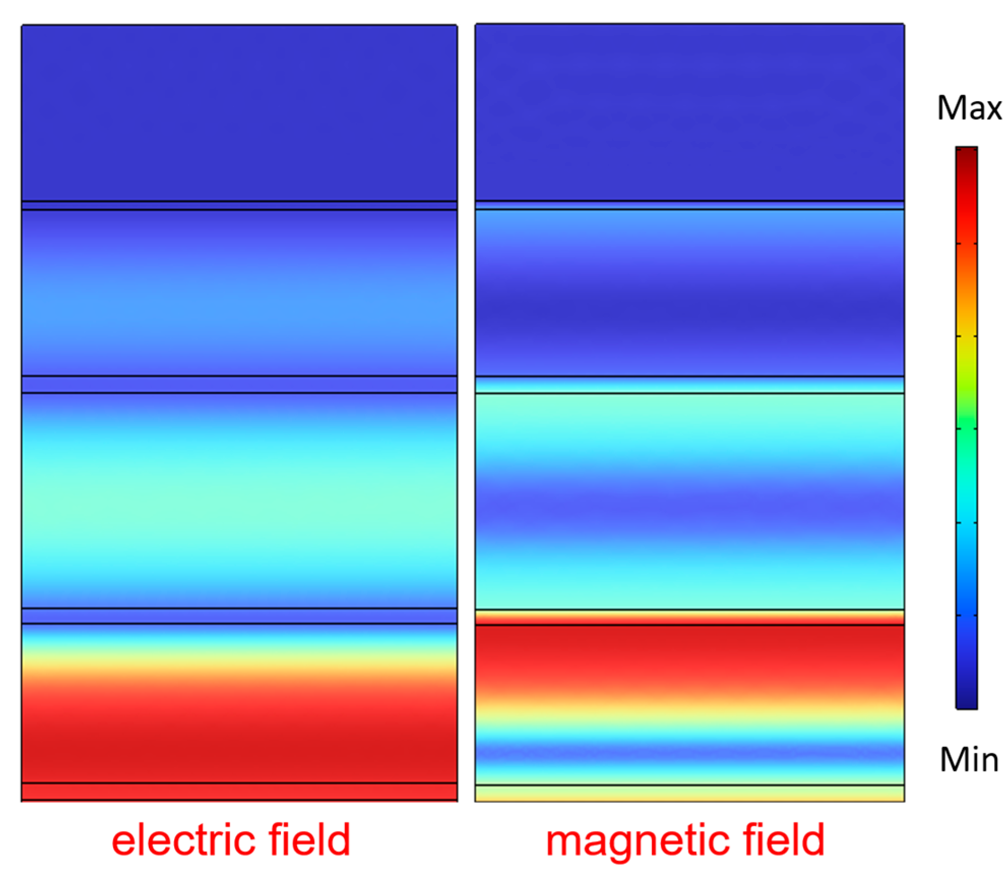
To demonstrate the underlying physical mechanisms responsible for the high absorptivity and ultra-broadband properties observed in the absorber under investigation, simulations were conducted to analyze the distributions of electric field intensities, as shown in
Figure 5a, and magnetic field intensities, as shown in
Figure 5b, in the x-z plane. The incident light used for exciting the absorber was TE-polarized and directed normally, with wavelengths of 430, 665, 880, and 1510 nm. These specific wavelengths were selected because they correspond to the absorption peaks displayed in the absorption spectrum of
Figure 3. These peaks indicate resonance reactions occurring within the material or structure being studied. Specifically, each absorption peak corresponds to a particular resonance mode at a specific wavelength, where the material or structure exhibits a significant enhancement of either the electric field or magnetic field at the specific wavelength. At these specific wavelengths, the electric field within the material or structure can become highly intensified, resulting in resonance. This amplified electric field can be effectively utilized to enhance the interaction between light and materials. Similarly, magnetic field analysis can be utilized to observe the distribution of the magnetic field at the wavelength wherein absorption peaks occur. At these wavelengths, the magnetic field associated with a structure or material may exhibit significant enhancement, leading to the formation of a resonance. This intensified magnetic field can be leveraged to augment light absorption or manipulate the characteristics of magnetic field-sensitive materials.
SPR is a remarkable phenomenon that arises in a thin metal sheet when it is illuminated by light at a precise angle, and SPR has the potential to be used as a technique for sensing or detecting specific substances (analytes). For example, SPR biosensors have been developed to detect various important biomarkers. The distinction between LSPR and PSPR primarily lies in the nature of the excitation and the range of the response. PSPR refers to the plasma oscillation caused by the interaction between light waves propagating through the metal surface and the electrons on the metal surface. It is an electromagnetic wave that propagates along a metal surface, and energy transfer occurs between the metal surface and a medium (usually a liquid). PSPR typically occurs on metal thin films or metal nanostructures, such as the interaction of light waves on metal thin films with metal/liquid interfaces. LSPR refers to the plasmonic oscillation caused by the interaction between light and electrons on the surface of metal nanoparticles or other nanostructures. Unlike PSPR, LSPR occurs locally, and its excitation is determined by the geometry, size, and composition of the nanostructure. LSPR typically results in strong absorption and scattering at the surface of metal nanoparticles, leading to characteristic absorption peaks in the visible spectral range. Therefore, it can be observed that the design primarily relies on LSPR for the absorption.
When incident light interacts with the surfaces of thin-film materials with alternating positive and negative permittivity, it initiates a phenomenon known as plasmon-induced transparency (PSP) resonance. This resonance is caused by the resonant oscillations of conduction electrons that take place at the interface of these materials. TE-polarized light at normal incidence was employed as the incident light to excite the investigated absorber at wavelengths of 430, 665, 880, and 1510 nm. These specific wavelengths were selected based on the absorption peaks of the absorption spectra observed in
Figure 2. As depicted in
Figure 5a, the distributions of electric field intensities resulting from normal incident TE-polarized light of various wavelengths exhibit coupling effects along the edge of the first MgF
2 layer. PSPR is the phenomenon wherein incident light couples to surface plasmons propagating along the interface of a metal film and a dielectric medium. Thus, the intensity of LSPR generally increases with film thickness up to a certain point, beyond which it either saturates or starts to decrease. This behavior occurs because thicker films can support more plasmon modes, resulting in enhanced light scattering or absorption. However, when the film exceeds a critical thickness, destructive interference between multiple plasmon modes can cause a reduction in LSPR intensity.
Figure 5a demonstrates that strong electric fields were present not only on the MgF
2 layer but also beneath the eight continuous films. The results shown in
Figure 6 confirm that across the incident light wavelengths of 430, 665, 880, and 1510 nm, the electric fields were primarily distributed throughout the entire absorber.
Furthermore,
Figure 5b presents magnetic field distributions corresponding to excitation wavelengths of 430, 665, 880, and 1510 nm. The results depicted in
Figure 5b distinctly indicate that the magnetic fields associated with various excitation wavelengths were distributed within the MgF
2 layer, top Ti layer, and top SiO
2 dielectric layer. The resonance of the Fabry–Perot (FP) cavity within an absorber can be achieved by incorporating two parallel flat semi-transparent metals to act as the reflective mirrors. In the specific absorber being investigated, the layers t7 (Ti), t5 (Ti), t3 (Mo), and t1 (Cu) are separated by dielectric layers made of lossless SiO
2 (t6, t4, and t2 layers). The lossless dielectric layers consist of SiO
2. Consequently, the metal layers t7-t5, t5-t3, and t3-t1, separated by SiO
2 layers, create two distinct FP cavities. The excitation wavelengths of 430, 665, 880, and 1510 nm satisfy the FP cavity resonance condition.
Figure 5b illustrates that the intensities of the magnetic field distributions, which originate from the FP cavity resonances occurring within the three SiO
2 cavity layers, exhibit variations corresponding to different excitation wavelengths. When normal incident light interacts with the absorber, it undergoes either constructive or destructive interference with the reflected light, leading to distinct patterns of magnetic field distribution. These magnetic distribution patterns provide clear evidence of the presence of FP cavity resonance within the SiO
2 dielectric layers. The magnetic field patterns depicted in
Figure 5b demonstrate that as the excitation wavelengths were set at 430, 665, 880, and 1510 nm, the plasmon-enhanced surface plasmon resonance (PSPR) was indeed excited in the MgF
2, upper Ti, and upper SiO
2 layers.
The calculated results demonstrate that the absorption characteristics of the studied absorber are significantly superior to those of the absorber with the eight-layer continuous plane films. This improvement can be attributed to the enhancements in the plasmon-induced PSPR and FP cavity resonances within the analyzed wavelength range.
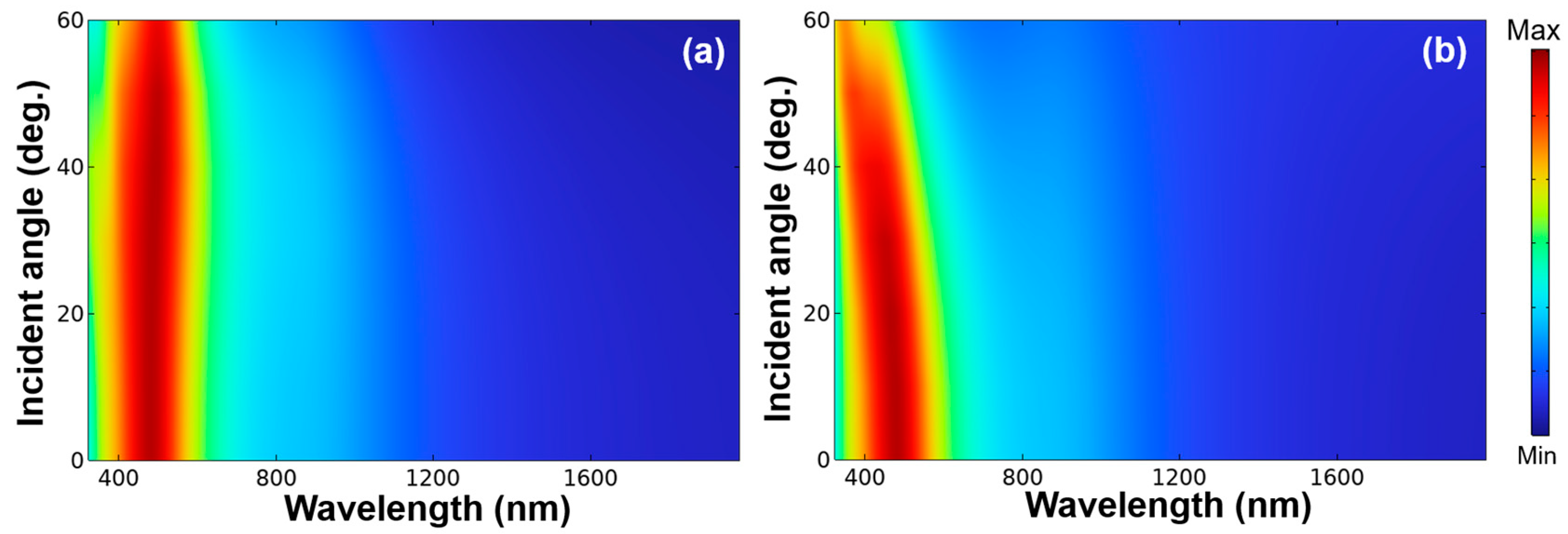
Figure 6 illustrates the evolution of absorption performance for incident light with angles ranging from 0 to 90 degrees, considering both TE and TM polarizations. The dotted line shown in
Figure 6 represents the approximate variation curve depicting absorptivity exceeding 90% for different incident angles and wavelengths. It is worth noting that when the absorber was stimulated under TE polarization and the wavelength ranged from 410 to 3000 nm, the absorber exhibited an absorptivity exceeding 90% for incident light angles between 0 degrees and approximately 45° to 65°. On the other hand, when the absorber was stimulated under TM polarization and the wavelength varied from 410 to 900 nm, the absorptivity exceeding 90% gradually decreased from around 60 degrees to approximately 50 degrees. Furthermore, as the wavelength surpassed 2000 nm and increased to 2400 nm, the absorptivity exceeding 90% experienced a decline from 50 degrees to 0 degrees. In particular, what is remarkable is that for both TE and TM polarizations, there is a situation wherein the absorptivity exceeds 90% between 85 and 90 degrees. These findings also indicate that the designed absorber possesses the characteristic of being insensitive to incident angles. Moreover, the absorber demonstrates excellent absorption performance, which is independent of polarization due to its highly symmetrical structure.
Next, we will examine the impact of different right metal materials on the absorptivity of the absorber designed in this study; the results are presented in
Figure 7. The materials compared in this study were Cu, Ni, Al, and Au, and it could be observed that there was minimal variation in absorption spectra among them. In other words, the choice of different metal materials for the right layer has virtually no effect on the absorption spectrum of the absorber designed in this study.
Figure 5 displays the distributions of electric field intensities and magnetic field intensities, illustrating that the right metal (Cu in
Figure 1) has limited influence on the absorptivity. Hence, no significant disparities in absorbance spectra were observed when utilizing different materials such as Cu, Ni, Al, and Au as substrates (all of the signal lines are overlapping, making it nearly impossible to distinguish each individual line clearly). However, our subsequent findings will demonstrate that the absorption spectrum and absorptivity of the excited light are greatly influenced by different metal materials when the light is excited from the direction of the right metal. The reasons for these results will be thoroughly discussed and substantiated.
To investigate the absorptive properties of the solar energy absorber, it is crucial to analyze its absorption of solar radiation.
Figure 8 depicts the calculated absorption of solar energy by the simulated absorber across the AM1.5 spectrum (from 280 nm to 4000 nm). A comparison of the absorption rates at different wavelength ranges can be found in
Table 1. Notably,
Table 1 illustrates that in the near-infrared range, the absorption rate reaches an impressive 99.32%. Within the absorption band spanning from 400 nm to 700 nm, from 700 nm to 1400 nm, and from 1400 nm to 3000 nm, the designed absorber can absorb 97.45%, 99.32%, and 99.26% of AM1.5G solar energy. The designed absorber exhibits a favorable absorption capacity under the AM1.5 solar spectrum, achieving an absorption rate of 94.76% within the absorption band spanning from 280 nm to 4000 nm. These findings indicate the efficiency of the designed absorber in absorbing solar energy across the visible, near-infrared, and mid-infrared ranges. Such absorption properties hold substantial value for solar-related applications, contributing significantly to solar conversion and energy harvesting endeavors. These results indicate that the designed absorber demonstrates nearly ideal wideband absorption across the visible and near-infrared spectrum. The wavelength range with high absorption aligns with the high-energy portion of the primary solar radiation.
Figure 9 depicts the absorption spectra of excitation of our specially designed multilayer film by illuminating it with light from the underlying metal’s direction. Through simulation, the absorption spectra of various light wavelengths can be analyzed in the multilayer composite film. When simulating different metal materials, the multilayer composite film exhibits varying characteristics of the absorption spectra. Analyzing the spectral performance of the absorber reveals distinct absorption curves for different metals. In particular, Cu presented a narrower peak in its absorption curve, indicating a higher absorptivity as compared to other metals. As
Figure 9 shows, when Cu is used as the metal, the remarkable 95.66% absorptivity within the 480 nm band suggests a robust LSPR effect. However, when Au, Al, and Ni were used as the metal, the absorption peaks were located at 495, 475, and 360 nm, and maximum absorptivity values were 93.0%, 91.3%, and 67.5%, exhibiting a noticeable decrease. Among the four metals considered, Au and Al exhibited slightly smaller absorption peaks than Cu, while Ni showed significantly smaller absorption peaks compared to these three metals. The detailed reasons for these variations will be discussed in the following paragraphs.
When a device has an absorption peak at 480 nm, it can potentially be used as a sensor for detecting or measuring light at that specific wavelength. The absorption peak indicates that the device strongly absorbs light with a wavelength of 480 nm. Based on this information, it is likely that the device in question is designed as a photodetector [
15].
Figure 10 shows that the analyses of both the electric field and magnetic field process at a wavelength of 480 nm. This observation indicates the presence of an LSPR reaction on the surface of the copper film. When light with a wavelength of 480 nm interacts with the copper surface, it excites the free electrons within the copper, leading to a resonant oscillation. On the copper surface, when the light wavelength is 480 nm, the free electrons in the copper are excited by the light, resulting in resonant oscillation. This resonant oscillation leads to a strong electric field enhancement effect on the copper surface, which in turn affects the light absorption, scattering, and coupling behavior. Specifically, at this wavelength, the electric field on the copper surface may be enhanced, creating regions of high electric field.
The relationship between these properties of absorptivity and conductivity of a material is very complex and can be influenced by various factors [
16,
17]. Thus, herein, we only discuss the relationship between the absorptivity and conductivity of a material. Absorptivity is a quantifiable metric representing the extent to which a material absorbs incident electromagnetic radiation. This parameter serves as a gauge for assessing the efficacy of the material in converting incoming radiation into internal energy. Absorptivity is measured on a scale from 0 to 1, with a value of 1 denoting the complete absorption of the incident radiation. Conversely, conductivity is a metric used to evaluate a material’s capacity to conduct electric current. It characterizes the material’s aptitude for facilitating the flow of electric charges, thereby determining its electrical conductivity. Conductivity is commonly represented by the symbol σ and is typically expressed in units of siemens per meter (S/m) or its inverse, resistivity (ρ), in ohm meters (Ω·m). When considering a metal film, the correlation between absorptivity and conductivity is influenced by the behavior of the metal’s free electrons. Metals exhibit excellent electrical conductivity due to their high concentration of free electrons, which can freely traverse the material. These free electrons are capable of interacting with incoming electromagnetic radiation, leading to energy absorption. When light or any other form of electromagnetic radiation interacts with a metal film, it undergoes various processes: reflection, transmission, and absorption.
The absorptivity of the metal film is determined by the interplay among these processes. Generally, as conductivity increases, the absorptivity also increases. This is because higher conductivity enables a more efficient interaction between the incident radiation and the free electrons within the metal film, resulting in enhanced absorption. As a result, highly conductive metals such as gold or silver are commonly employed in applications that necessitate high absorptivity, such as solar cells or heat absorbers. Nevertheless, it is crucial to recognize that the correlation between absorptivity and conductivity is not a simple linear relationship. Other factors, such as the thickness of the metal film, the wavelength of the incident radiation, and the presence of surface features or coatings, can also impact the absorption characteristics. The ρ (resistivity) values of Cu, Au, Al, and Ni are 1.68 × 10⁻⁸ Ω·m, 2.44 × 10⁻⁸ Ω·m, 2.65 × 10⁻⁸ Ω·m, and 6.99 × 10⁻⁸ Ω·m, respectively. Comparing the characteristics of these metals, it is evident that higher conductivity in a metal corresponds to a significantly larger absorptivity at 480 nm. This outcome demonstrates that when a metal is employed as the incident layer for light waves in an absorber, greater conductivity leads to improved performance. Therefore, while a higher conductivity generally leads to higher absorptivity in metal films.
Figure 11 presents the response of our designed multilayer film when illuminated from the direction of the copper metal. Only around the band of 480 nm wavelength range does the real part (depicted by the black solid line) of this absorber approach unity, indicating minimal impact on the speed of light propagation. The imaginary part (shown by the red solid line) of the 480 nm band approaches zero, suggesting reduced energy loss in this range. Furthermore, the results in
Figure 11 reaffirm the crucial role of optical impedance in determining absorptivity.
Figure 12 shows the absorptivity of TE-polarized light and TM-polarized light with normal direction and various oblique incidence angles for the application of a narrowband sensor. In the absorption diagrams for with angles ranging from 0 to 60 degrees and TM with angles ranging from 0 to 50 degrees, there is strong absorption at 480 nm. This suggests that the designed device does not significantly affect the absorption properties with respect to the angle of incidence. In other words, regardless of the incident angle, the absorption effect remains consistent.


