Crystalline Flat Surface Recovered by High-Temperature Annealing after Laser Ablation

 , , and
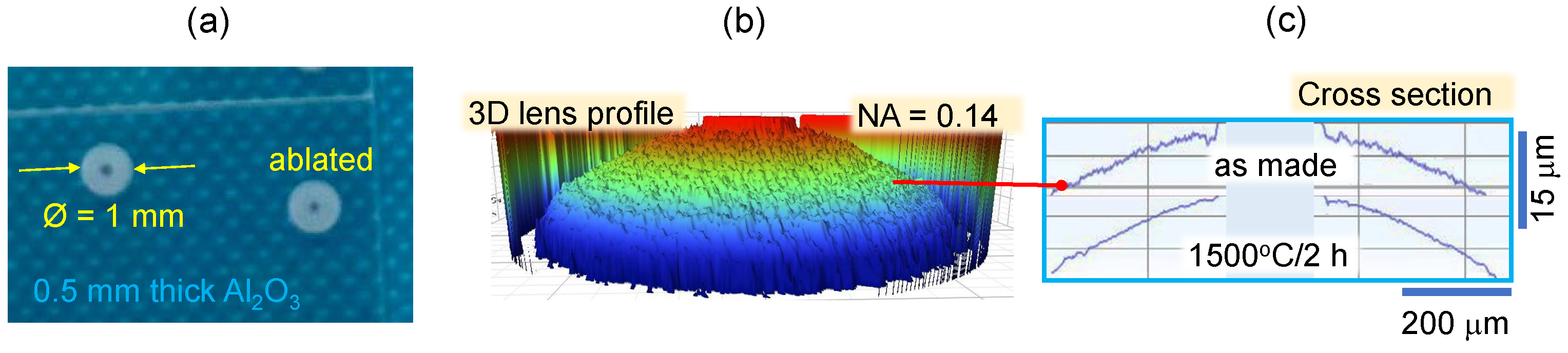
Abstract
:1. Introduction: High Intensity > TW/cm Crystal Processing
2. Samples and Methods
2.1. Sapphire
2.2. Laser Ablation Conditions
2.3. High-Temperature Annealing
3. Results and Discussion
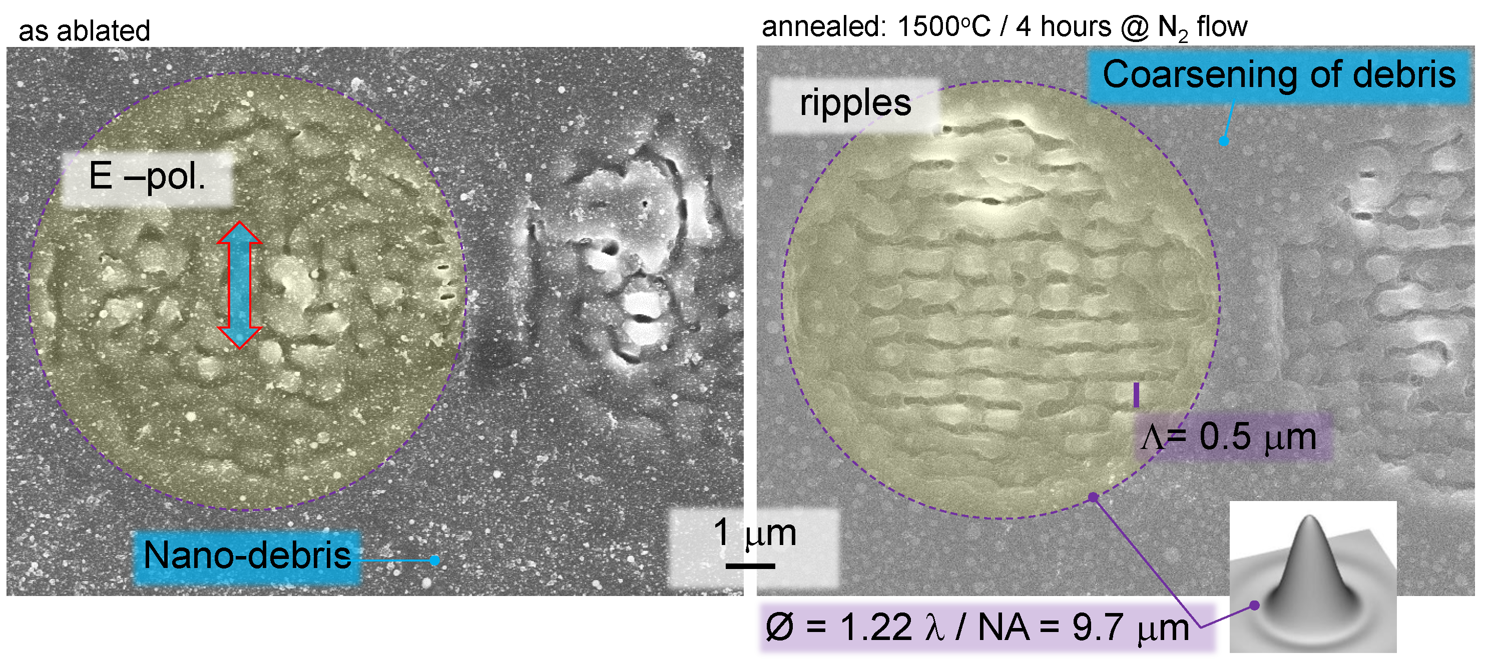
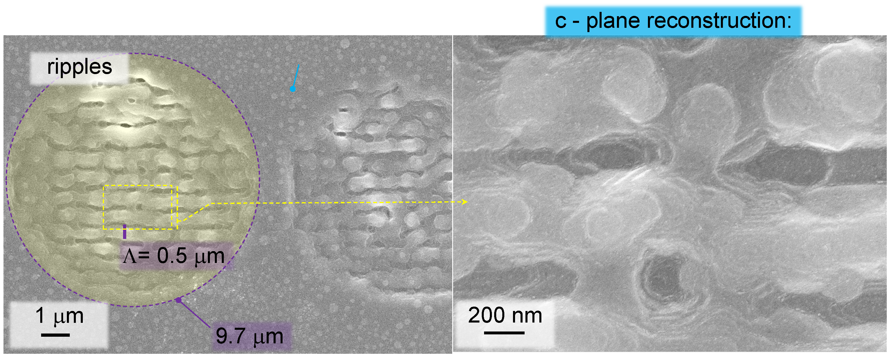
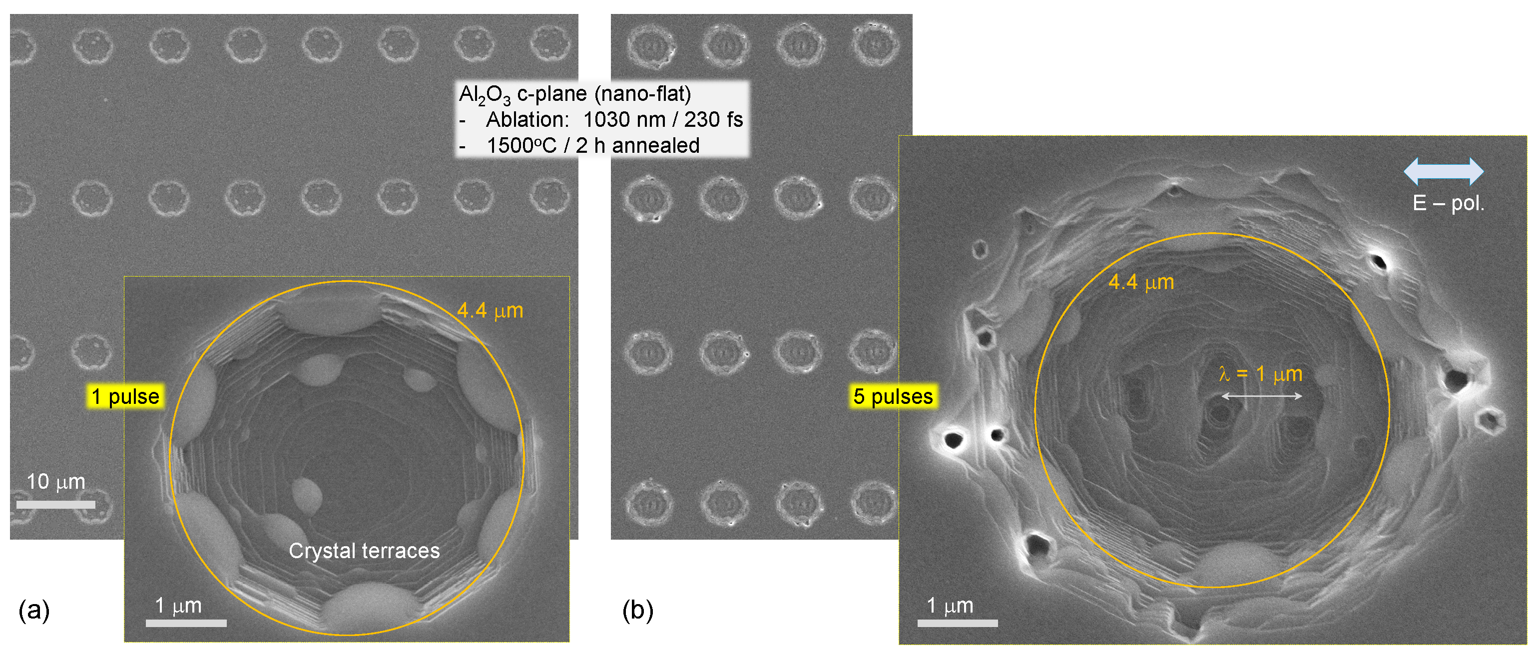
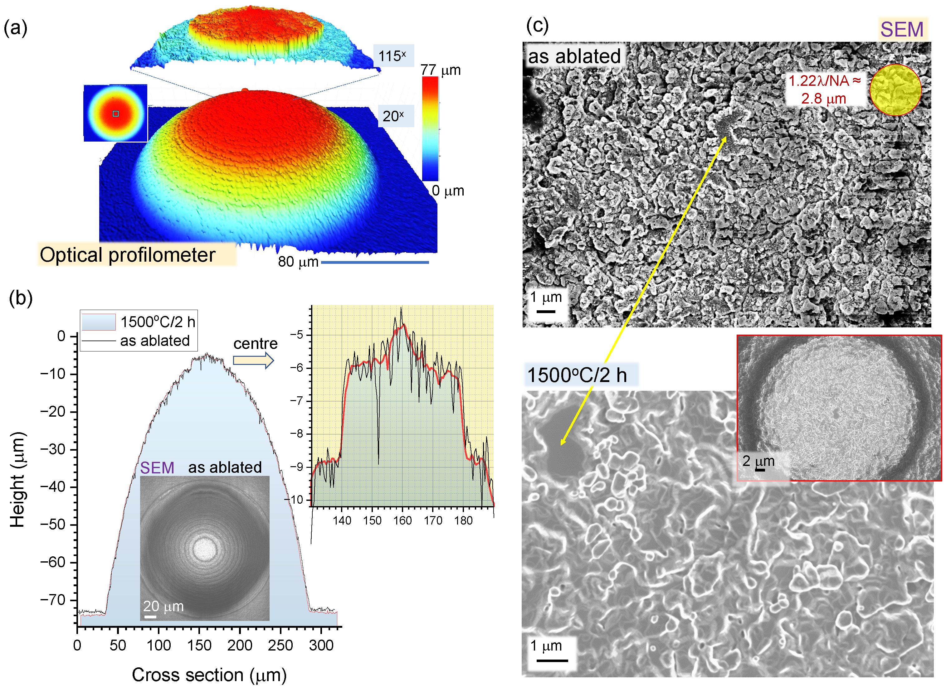
3.1. Roughness Reduction of Ablated Sapphire Surfaces
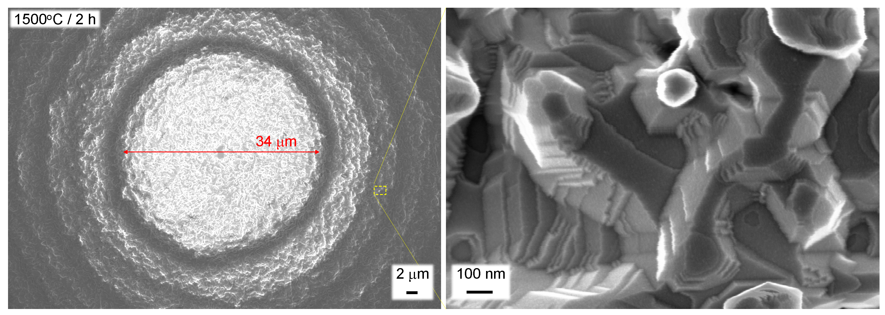
3.2. Recovery of Crystalline Smooth Surface on Ablated Sapphire
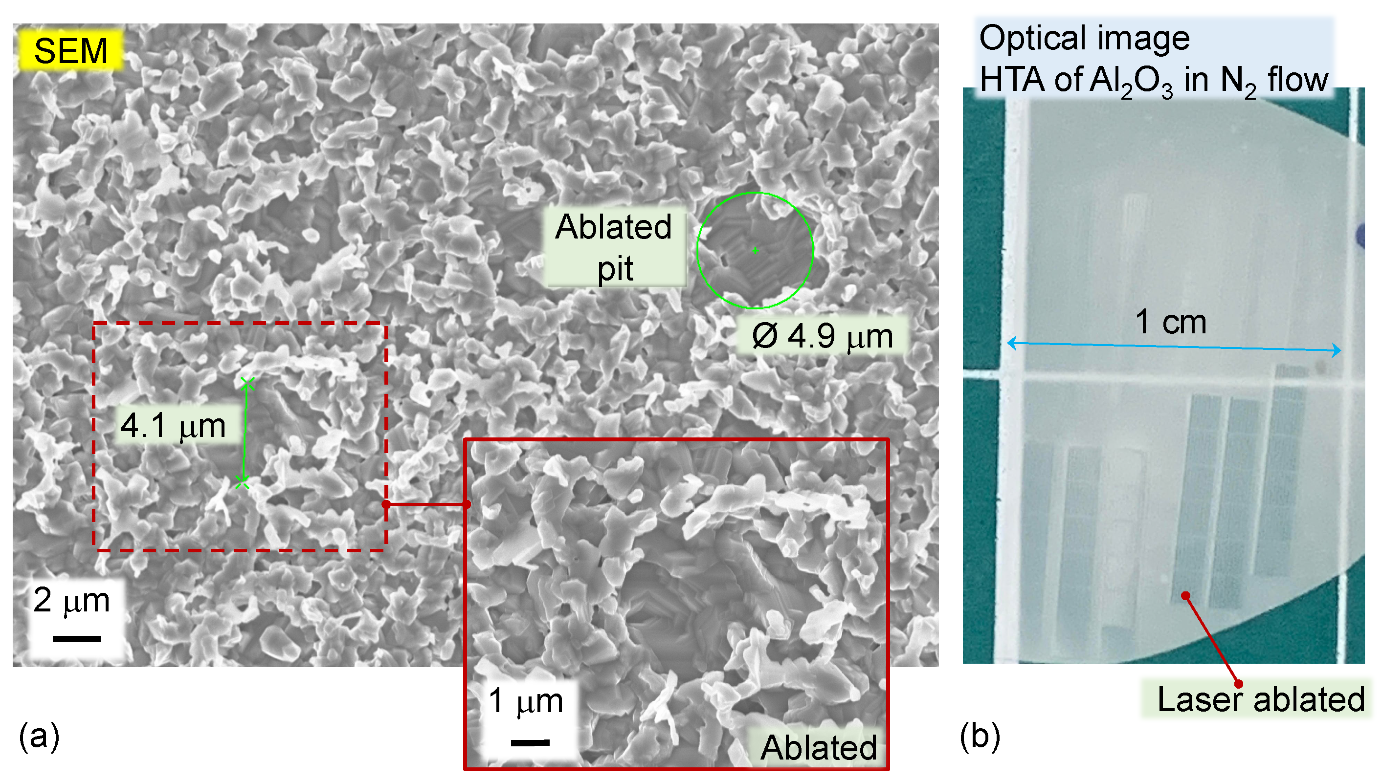
3.3. HTA Treatment of Back-Side Ablated Al2O3
4. Conclusions and Outlook
Author Contributions
Funding
Institutional Review Board Statement
Informed Consent Statement
Data Availability Statement
Conflicts of Interest
Appendix A. HTA of Al2O3 in N2

References
- Batani, K.; Batani, D.; He, X.; Shigemori, K. Recent progress in matter in extreme states created by laser. Matter Radiat. Extrem. 2022, 7, 013001. [Google Scholar] [CrossRef]
- Juodkazis, S.; Nishimura, K.; Tanaka, S.; Misawa, H.; Gamaly, E.E.; Luther-Davies, B.; Hallo, L.; Nicolai, P.; Tikhonchuk, V. Laser-Induced Microexplosion Confined in the Bulk of a Sapphire Crystal: Evidence of Multimegabar Pressures. Phys. Rev. Lett. 2006, 96, 166101. [Google Scholar] [CrossRef] [PubMed]
- Vailionis, A.; Gamaly, E.G.; Mizeikis, V.; Yang, W.; Rode, A.; Juodkazis, S. Evidence of super-dense Aluminum synthesized by ultra-fast micro-explosion. Nat. Commun. 2011, 2, 445. [Google Scholar] [CrossRef] [PubMed]
- Zelovich, Y.B.; Raizer, Y.P. Physics of Shock Waves and High-Temperature Hydrodynamic Phenomena; Dover, Dover Books on Physics: New York, NY, USA, 2002. [Google Scholar]
- Campanella, B.; Legnaioli, S.; Pagnotta, S.; Poggialini, F.; Palleschi, V. Shock waves in laser-induced plasmas. Atoms 2019, 7, 57. [Google Scholar] [CrossRef]
- Juodkazis, S.; Nishimura, K.; Misawa, H.; Ebisui, T.; Waki, R.; Matsuo, S.; Okada, T. Control over the State of Crystallinity: Sapphire. Adv. Mat. 2006, 18, 1361–1364. [Google Scholar] [CrossRef]
- Huang, H.H.; Juodkazis, S.; Gamaly, E.; Nagashima, T.; Yonezawa, T.; Hatanaka, K. Spatio-temporal control of THz emission. Commun. Phys. 2022, 5, 134. [Google Scholar] [CrossRef]
- Juodkazis, S.; Misawa, H.; Gamaly, E.G.; Luther-Davis, B.; Hallo, L.; Nicolai, P.; Tikhonchuk, V. Is the nano-explosion really microscopic? J. Non-Crystall. Solids 2009, 355, 1160–1162. [Google Scholar] [CrossRef]
- Nath, G. Approximate analytical solution for the propagation of shock waves in self-gravitating perfect gas via power series method: Isothermal flow. J. Astrophys. Astron. 2020, 41, 21. [Google Scholar] [CrossRef]
- Sharova, Y.S.; Glazyrin, S.I.; Gasilov, V.A. Study of the Influence of the Background Neutral Component on the Dynamics of the Envelope in Supernova Remnants. Astron. Lett. 2021, 47, 746–753. [Google Scholar] [CrossRef]
- Petruk, O.; Kuzyo, T.; Orlando, S.; Pohl, M.; Brose, R. Magneto-hydrodynamic simulations of young supernova remnants and their energy-conversion phase. Mon. Not. R. Astron. Soc. 2021, 505, 755–770. Available online: https://academic.oup.com/mnras/article-pdf/505/1/755/39549986/stab1319.pdf (accessed on 1 May 2023). [CrossRef]
- Hirashima, K.; Moriwaki, K.; Fujii, M.; Hirai, Y.; Saitoh, T.; Makino, J. Predicting the Expansion of Supernova Shells Using Deep Learning toward Highly Resolved Galaxy Simulations. Proc. Int. Astron. Union 2020, 16, 209–214. [Google Scholar] [CrossRef]
- Hua, J.G.; Liang, S.Y.; Chen, Q.D.; Juodkazis, S.; Sun, H.B. Free-Form Micro-Optics Out of Crystals: Femtosecond Laser 3D Sculpturing. Adv. Func. Mat. 2022, 32, 2200255. [Google Scholar] [CrossRef]
- Marupalli, B.C.; Adhikary, T.; Sahu, B.; Mitra, R.; Aich, S. Effect of annealing temperature on microstructure and mechanical response of sputter deposited Ti-Zr-Mo high temperature shape memory alloy thin films. Appl. Surf. Sci. Adv. 2021, 6, 100137. [Google Scholar] [CrossRef]
- Shklyaev, A.; Latyshev, A. Surface Morphology Transformation Under High-Temperature Annealing of Ge Layers Deposited on Si(100). Nanoscale Res. Lett. 2016, 11, 366. [Google Scholar] [CrossRef] [PubMed]
- Woo, S.; Jeong, H.; Lee, S.; Seo, H.; Lacotte, M.; David, A.; Kim, H.; Prellier, W.; Kim, Y.; Choi, W.S. Surface properties of atomically flat poly-crystalline SrTiO3. Sci. Rep. 2015, 5, 8822. [Google Scholar] [CrossRef]
- Gailevicius, D.; Padolskyte, V.; Mikoliunaite, L.; Sakirzanovas, S.; Juodkazis, S.; Malinauskas, M. Additive-manufacturing of 3D glass-ceramics down to nanoscale resolution. Nanoscale Horiz. 2019, 4, 647–651. [Google Scholar] [CrossRef]
- Acosta-Alba Pablo, E.; Kononchuk, O.; Gourdel, C.; Claverie, A. Surface self-diffusion of silicon during high temperature annealing. J. Appl. Phys. 2014, 115, 134903. [Google Scholar] [CrossRef]
- Liu, M.; Zhou, H.; Zhu, H.; Yue, Z.; Zhao, J. Microstructure and dielectric properties of glass/Al2O3 composites with various low softening point borosilicate glasses. J. Mater. Sci. Mater. Electron. 2012, 23. [Google Scholar] [CrossRef]
- Uwaha, M.; Saito, Y. Kinetic smoothing and roughening of a step with surface diffusion. Phys. Rev. Lett. 1992, 68, 224–227. [Google Scholar] [CrossRef]
- Zaluska-Kotur, M.A.; Krzyzewski, F.; Krukowski, S.; Czernecki, R.; Leszczynski, M. Structures Built by Steps Motion during Sublimation from Annealed GaN(0001) Surface. Cryst. Growth Des. 2013, 13, 1006–1013. [Google Scholar] [CrossRef]
- Kazantsev, D.; Akhundov, I.; Rudaya, N.; Kozhukhov, A.; Alperovich, V.; Latyshev, A. Thermal roughening of GaAs surface by unwinding dislocation-induced spiral atomic steps during sublimation. Appl. Surf. Sci. 2020, 529, 147090. [Google Scholar] [CrossRef]
- Kazantsev, D.; Akhundov, I.; Karpov, A.; Shwartz, N.; Alperovich, V.; Terekhov, A.; Latyshev, A. Monte Carlo simulation of GaAs(001) surface smoothing in equilibrium conditions. Appl. Surf. Sci. 2015, 333, 141–146. [Google Scholar] [CrossRef]
- Mundschau, M.; Bauer, E.; Telieps, W.; Swieh, W. Atomic steps on Si100 and step dynamics during sublimation studied by low-energy electron microscopy. Surf. Sci. 1989, 223, 413–423. [Google Scholar] [CrossRef]
- Sheglov, D.V.; Sitnikov, S.V.; Fedina, L.I.; Rogilo, D.I.; Kozhukhov, A.S.; Latyshev, A.V. From Self-Organization of Monoatomic Steps on the Silicon Surface to Subnanometer Metrology. Optoelectron. Instrum. Data Process. 2020, 56, 533–544. [Google Scholar] [CrossRef]
- Readey, D.; Kuczynski, G. Sublimation of Aluminum Oxide in Hydrogen. J. Am. Ceram. Soc. 2006, 49, 26–29. [Google Scholar] [CrossRef]
- Andre, P.; Abbaoui, M.; Augeard, A.; Desprez, P.; Singo, T. Study of Condensed Phases, of Vaporization Temperatures of Aluminum Oxide and Aluminum, of Sublimation Temperature of Aluminum Nitride and Composition in an Air Aluminum Plasma. Plasma Chem. Plasma Process. 2016, 36, 1161–1175. [Google Scholar] [CrossRef]
- Gamaly, E.E.; Juodkazis, S.; Nishimura, K.; Misawa, H.; Luther-Davies, B.; Hallo, L.; Nicolai, P.; Tikhonchuk, V. Laser-matter interaction in a bulk of a transparent solid: Confined micro-explosion and void formation. Phys. Rev. B 2006, 73, 214101. [Google Scholar] [CrossRef]
- Hua, J.G.; Ren, H.; Huang, J.; Luan, M.L.; Chen, Q.D.; Juodkazis, S.; Sun, H.B. Laser-Induced Cavitation-Assisted True 3D Nano-Sculpturing of Hard Materials. Small 2023, 2207968. [Google Scholar] [CrossRef]
- Liu, X.Q.; Zhang, Y.L.; Li, Q.K.; Zheng, J.X.; Lu, Y.M.; Juodkazis, S.; Chen, Q.D.; Sun, H.B. Biomimetic sapphire windows enabled by inside-out femtosecond laser deep-scribing. PhotoniX 2022, 3, 1. [Google Scholar] [CrossRef]
- Mahesh, J.Y.; Aravindan, S.; Rao, P.V.; Yogita, M.; Singh, J.P. Surface morphology evolution of C-plane sapphire during multi-step thermal annealing. Surf. Topogr. Metrol. Prop. 2022, 10, 045015. [Google Scholar] [CrossRef]
- Prosvirnin, D.V.; Kolmakov, A.G.; Larionov, M.D.; Prutskov, M.E.; Alikhanyan, A.S.; Samokhin, A.V.; Lysenkov, A.S.; Titov, D.D. Effect of sintering methods and temperatures on porosity of the ceramics from aluminum oxinitride. IOP Conf. Ser. Mater. Sci. Eng. 2018, 347, 012030. [Google Scholar] [CrossRef]
- Kudrius, T.; Šlekys, G.; Juodkazis, S. Surface-texturing of sapphire by femtosecond laser pulses for photonic applications. J. Phys. D: Appl. Phys. 2010, 43, 145501. [Google Scholar] [CrossRef]
- Buividas, R.; Aharonovich, I.; Seniutinas, G.; Wang, X.W.; Rapp, L.; Rode, A.V.; Juodkazis, S. Photoluminescence from voids created by femtosecond-laser pulses inside cubic-BN. Opt. Lett. 2015, 40, 5711–5713. [Google Scholar] [CrossRef] [PubMed]
- Hsu, W.H.; Masim, F.; Balcytis, A.; Juodkazis, S.; Hatanaka, K. Dynamic position shifts of X-ray emission from a water film induced by a pair of time-delayed femtosecond laser pulses. Opt. Express 2017, 25, 24109–24118. [Google Scholar] [CrossRef]
- Gamaly, E.G.; Rode, A.V. Ultrafast re-structuring of the electronic landscape of transparent dielectrics: New material states (Die-Met). Appl. Phys. A 2018, 124, 278. [Google Scholar] [CrossRef]
- Ng, S.; Juodkazis, S. Nanoscale Plasmonic Printing in Ultrafast Laser Nanostructuring: The Pursuit of Extreme Scales; Stoian, R., Bonse, J., Eds.; Springer Series in Optical Science; Springer: Berlin/Heidelberg, Germany, 2023; Volume 239, Chapter 25. [Google Scholar]
- Buividas, R.; Mikutis, M.; Juodkazis, S. Surface and bulk structuring of materials by ripples with long and short laser pulses: Recent advances. Prog. Quantum Electron. 2019, 38, 119–156. [Google Scholar] [CrossRef]
- Vanagas, E.; Kudryashov, I.; Tuzhilin, D.; Juodkazis, S.; Matsuo, S.; Misawa, H. Surface nanostructuring of borosilicate glass by femtosecond nJ energy pulses. Appl. Phys. Lett. 2003, 82, 2901–2903. [Google Scholar] [CrossRef]
- Bach, H.; Krause, D. Technical Glasses—Physical and Technical Properties. In Technical Report; SCHOTT AG: Mainz, Germany, 2020. [Google Scholar]


Disclaimer/Publisher’s Note: The statements, opinions and data contained in all publications are solely those of the individual author(s) and contributor(s) and not of MDPI and/or the editor(s). MDPI and/or the editor(s) disclaim responsibility for any injury to people or property resulting from any ideas, methods, instructions or products referred to in the content. |
© 2023 by the authors. Licensee MDPI, Basel, Switzerland. This article is an open access article distributed under the terms and conditions of the Creative Commons Attribution (CC BY) license (https://creativecommons.org/licenses/by/4.0/).
Share and Cite
Smith, D.; Ng, S.H.; Tang, A.; Katkus, T.; Moraru, D.; Juodkazis, S. Crystalline Flat Surface Recovered by High-Temperature Annealing after Laser Ablation. Photonics 2023, 10, 594. https://doi.org/10.3390/photonics10050594
Smith D, Ng SH, Tang A, Katkus T, Moraru D, Juodkazis S. Crystalline Flat Surface Recovered by High-Temperature Annealing after Laser Ablation. Photonics. 2023; 10(5):594. https://doi.org/10.3390/photonics10050594
Chicago/Turabian StyleSmith, Daniel, Soon Hock Ng, Amanda Tang, Tomas Katkus, Daniel Moraru, and Saulius Juodkazis. 2023. "Crystalline Flat Surface Recovered by High-Temperature Annealing after Laser Ablation" Photonics 10, no. 5: 594. https://doi.org/10.3390/photonics10050594