Article

A Novel Isolated Intelligent Adjustable Buck-Boost Converter with Hill Climbing MPPT Algorithm for Solar Power Systems

1
Department of Electrical Engineering, National Taiwan University of Science and Technology, Taipei 106, Taiwan
2
Department of Electrical Engineering, National Chin-Yi University of Technology, Taichung 411, Taiwan
3
Undergraduate Program of Vehicle and Energy Engineering, National Taiwan Normal University, Taipei 106, Taiwan
4
Department of Electrical Engineering, ZHCET, Aligarh Muslim University, Aligarh 202002, India
5
Graduate Institute of Manufacturing Technology, National Taipei University of Technology, Taipei 106, Taiwan
*
Author to whom correspondence should be addressed.
Processes 2023, 11(4), 1010; https://doi.org/10.3390/pr11041010
Submission received: 5 March 2023 / Revised: 23 March 2023 / Accepted: 25 March 2023 / Published: 27 March 2023

Abstract

:
This study proposes a new isolated intelligent adjustable buck-boost (IIABB) converter with an intelligent control strategy that is suitable for regenerative energy systems with unsteady output voltages. It also serves as a reliable voltage source for loads such as battery systems, microgrids, etc. In addition, the hill climbing (HC) maximum power point tracking (MPPT) algorithm can be utilized with this innovative IIABB converter to capture the MPP and then enhance system performance. In this converter, five inductors (LA, LB, LC, LD, and LE) and four power MOSFETs (SA, SB, SC, and SD) are used in the proposed novel isolated intelligent adjustable buck-boost (IIABB) converter to adjust the applied voltage across the load side. It also has a constant, stable output voltage. The new IIABB converter is simulated and verified using MATLAB R2021b, and the performances of the proposed IIABB converter and conventional SEPIC converter are compared. The solar photovoltaic module output voltages of 20 V, 30 V, and 40 V are given as inputs to the proposed IIABB converter, and the total output voltage of the proposed converter is 48 V. In the new IIABB converter, the duty cycle of the power MOSFET has a small variation. The proposed IIABB converter has an efficiency of 92~99%. On the other hand, in the conventional SEPIC converter, the duty cycle of a power MOSFET varies greatly depending on the relationship between the output and input voltage, which deteriorates the efficiency of the converter. As a result, this research contributes to the development of a novel type of IIABB converter that may be employed in renewable energy systems to considerably increase system performance and reduce the cost and size of the system.

1. Introduction

Today, the need for electricity generation from renewable sources is rising for both residential and industrial purposes. Power generation from fossil fuels results in the emission of hazardous substances into the atmosphere. These fossil fuels are declining in the environment over time. Solar energy is one of the most abundant, eco-friendly, and pollution-free renewable energy sources. Using the photovoltaic (PV) effect, a solar cell converts sunlight into electricity. Once a solar energy system is installed, it should be able to operate for an extended period and save money and overall maintenance costs. As a result of its adaptable nature, solar energy can be utilized for a variety of power applications, ranging from little torches to satellites. Conventional energy sources are under imminent threat of extinction. As a result, the new electrical technology is more dependent on non-conventional or renewable energy sources. In the absence of the consistent and continuous output of nonconventional power sources (solar PV, wind turbines, fuel cells, and hybrid PV/fuel cell/wind turbines), power cannot be sent directly to the load (such as a DC microgrid, a DC home, an electric vehicle, or HVDC transmission, etc.). For charging applications, a high-efficiency and continuous DC–DC power converter is employed to address these disadvantages of renewable energy sources. In addition to PV panels, solar PV systems use power electronic converters to connect their output to the grid or to local loads. DC–DC converters and DC–AC inverters are commonly used power electronics converters. With the MPPT algorithm integrated with the DC–DC converter, the DC–DC converter steps up/down the input voltage of the solar PV array to maximize the power output. Whenever power semiconductor devices are used as switches, electrical interference and power loss are introduced due to the internal resistance of the switches and inductors. It results in a decrease in efficiency and power quality due to these problems. It is imperative to create efficient DC-DC converters and effective MPPT algorithms to mitigate these issues. This paper proposes an isolated intelligent adjustable buck-boost (IIABB) with a coupled inductor wound on a single core for battery charging, which leads to a reduction in the size of the whole setup and hence reduces the current ripple, as discussed in detail. Some applications of the proposed (IIABB) converter are shown in Figure 1.
Various converters exist to satisfy the aforementioned demand; some are discussed here. In a study [1], the author uses a single-ended primary inductance converter (SEPIC) with a passive component in PV systems that require regulated output voltage. The result shows that SEPIC converters are well suited for smooth induction motor speed control. Adaptive nonlinear methods are proposed in [2] for tracking a SEPIC’s maximum power point (MPP) and regulating its output voltage. Work [3] employs the bridgeless SEPIC converter for battery charging applications. This system can rectify and convert DC to DC with an improved power factor and low harmonics. In [4], a current sensor-based maximum power point tracking (MPPT) algorithm with adaptive step size is proposed for a solar photovoltaic system based on a SEPIC. Because power is less sensitive to current perturbation than voltage is, the author [5] proposes a high voltage gain SEPIC structure for use in renewable energy applications; such a scheme is seen as a novel SEPIC structure. This shows that the modified SEPIC converter has a higher voltage gain than a conventional SEPIC or the recently discussed single-controlled switch converter. The study [6] presents a novel non-isolated single switch quadratic modified SEPIC converter with high voltage gain. To achieve the suggested, the converter combines a modified SEPIC converter with a boosting module to attain a large voltage gain at a low duty ratio [7], which presents the theory of a new DC-DC power converter’s theoretical assessment and numerical simulations of the SEPIC topology. A three-port dual boost SEPIC converter is described in this article [8] for use in a hybrid PV/battery electric vehicle to enhance the efficiency and capability of the power conversion stage. In this work [9], the perturb and observe (P&O) and incremental conductance (IC) algorithms are used to determine the duty cycle of the SEPIC’s pulse width modulation (PWM), which is used to control the system’s operation point. The study [10] is centered on the dimensioning and modeling of a continuous conduction mode SEPIC converter. In work [4], the efficiency of standard Boost and SEPIC converters was evaluated and compared to the updated SEPIC converter. This article [11] proposes a simple soft-switching structure adaptable to the various configurations of the modified SEPIC converter, thereby lowering switching losses and diode reverse recovery current. Article [12] utilizes a DC-DC converter with the Cuk-SEPIC configuration, resulting in increased power efficiency and cost savings, especially when used with unnecessary filters. Using a constructed model and a simulink model, this paper [13] compares the conventional SEPIC and cascaded boost–SEPIC converters in detail. This study suggested a new global maximum power point tracking (global-MPPT) method [14]. Under partial shading conditions, the algorithm avoids the P&O technique disturbance problem caused by power points trapped at the local peak point. The work [15] proposes an extendable triple-port SEPIC (TPS) converter as a compact and efficient multiport interface with fewer components for integrating renewable energy sources in a microgrid system. In this publication [16], a PID controller for the SEPIC converter was developed, and the system’s performance was investigated when the reference voltage output changed. This study demonstrates that coupling a PID controller to a SEPIC converter is effective in terms of design, analysis, and convenience, as it acts as a step-up and step-down voltage regulator. This article [17] discusses the integration topology of a DC-DC SEPIC converter with a full-bridge DC-AC inverter. The proposed topology can convert the low DC voltage to a higher AC voltage by connecting the circuits in parallel. According to this article [18], the PWM method is used to implement a safe adaptive controller for a non-minimum phase SEPIC converter based on robust adaptive control. The article [19] discusses the comparison of the recently proposed multilevel inverter (MLI). An analysis is conducted in this paper [20] of two proposed models with two distinct modified SEPIC converters, with and without magnetic windings for increased output voltage. In [21], a highly recommended novel maximum power point tracking method is introduced for PV applications derived from the proposed method with the help of the secant incremental gradient method, which is based on the Newton–Rapson method. The moth frame optimizer-perturb and observe method [22] is used to implement the MPPT problem in the PV system. In [23], a hybrid method based on the gray wolf optimizer-crow search algorithm is proposed. This control strategy can efficiently capture the maximum power point under partially shaded and fast-changing irradiance level conditions. The optimization of photovoltaic systems in partial shading conditions is solved with TFWO [24], which is based on the formation of whirlpools in a turbulent flow of water. In order to maximize the power extracted from the photovoltaic system, the optimal duty cycle is determined using the TFWO.
To meet requirements for a constant output voltage from the converter and increase system performance, there needs to be a reduction in the cost and size of the system. A novel type of isolated intelligent adjustable buck-boost (IIABB) converter is introduced.
This paper has been categorized into five sections. The introduction has been discussed in Section 1. Section 2 introduces the conventional SEPIC converter. Section 3 provides a description of the new IIABB converter and HC algorithm. Our simulation and experimental results are presented in Section 4, and in the last section of this paper, conclusions and future directions are presented.

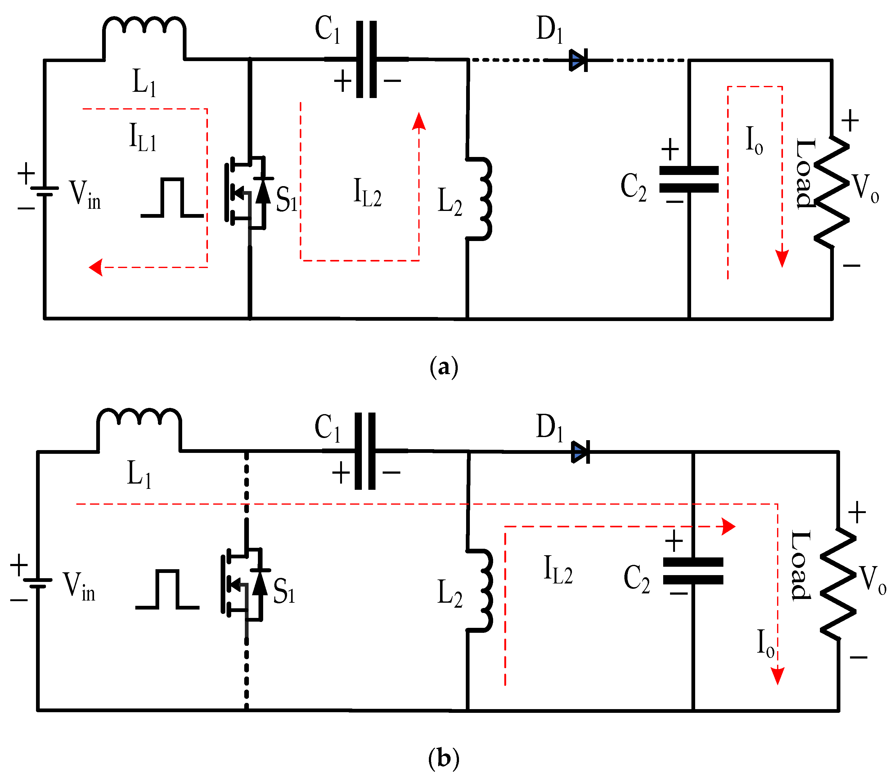
2. Conventional SEPIC Converter

To step down or up the input voltage, such types of converters are used in a buck-boost topology (as shown in Figure 2). The SEPIC produces an output voltage that either exceeds or falls below the input voltage without reversing the polarity. The SEPIC converter provides the regulated output voltage regardless of whether the input voltage is higher or lower than the constant output voltage. Conventional DC-DC converters are unable to achieve high voltage gain due to their high duty cycles, switching frequencies, transformer requirements, and system size [1,2,3,4,5]. To feed a grid-connected inverter, the low voltage from renewable energy sources must be boosted. The main aim of this paper is to introduce the proposed converters, which are the extended form of this conventional topology.
It is primarily dependent on the duty cycle and parasitic elements in the circuit that determine how much the SEPIC converter steps up or down the level of voltage. The output voltage VO of the SEPIC converter can be calculated.
V O = D V i 1 D
where Vi represents the input voltage and D represents the duty cycle.
However, it doesn’t contain any parasitic losses such as diode drop losses. Therefore, the equation is as follows:
V O + V D = D V i 1 D
This becomes the following:
D = V O + V D V i + V O + V D
For the continuous conduction mode (CCM) of operation, the computation value of the inductor L1 = L2 is represented by the equation below:
L 1 = L 2 = V i m i n + D m a x Δ i o m a x + f s w
where, Vimin is the absolute minimum voltage that can be fed into the converter, Dmax represents the maximum duty cycle, fsw represents switching frequency, and Δ i o m a x represents an acceptable output current ripple.
The SEPIC converter is similar to the buck-boost converter, but it has the advantage of having a non-inverting output voltage. A series capacitor is used to transfer energy from a source to a load and is capable of true shutdown. The equivalent circuit of a SEPIC converter, as shown in Figure 2, is as follows: When the switch S1 is ON, the current IL2 starts increasing, and the current across inductor L1, which comes from the instantaneous voltage source, is approximately equivalent to the input voltage Vin, the diode D1 is opened, the input capacitor C1 supplies the energy, and it operates according to the waveform during time 0–t0 as shown in Figure 3. When S1 is OFF, the current across the capacitor C1 becomes equal to the IL1, therefore the inductor does not allow instantaneous changes in current. The current flows across the inductor L2 in a negative direction. This is because if the switch is closed long enough for a half cycle of resonance with inductor L2, the potential (voltage) across capacitor C1 will remain the same, which can be seen clearly with the help of the waveform during time t0–t1 as shown in Figure 3. Two inductors, L1 and L2, a diode D1, a power MOSFET S1, an output capacitor C2, and a coupling capacitor C1 are used in the converter. Due to the presence of a coupling capacitor with negative polarity, diode D1 is reverse biased upon activation. When the coupling capacitor discharges, both the inductors L1 and L2 get charged. During this time, the diode is turned off, and it becomes forward biased. Inductor L1 transfers energy to the coupling capacitor, while inductor L2 delivers energy to the output terminal. The L1 and L2 inductors can be coiled on a single core, and they can receive the same switching period voltage. A coupled inductor minimizes the size of the whole circuitry and the overall cost of the system.
Figure 3 demonstrates the converter switching waveforms. Vin is the input voltage across the power MOSFET S1 when it is turned on and off. IS1 represents current across the power MOSFET S1, IC1 represents current across the coupling capacitor, and IL1 and IL2 inductor currents build linearly. ID1 is the diode current, IC1 is the current through the coupling capacitor, and IC2 is the current through the output capacitor.

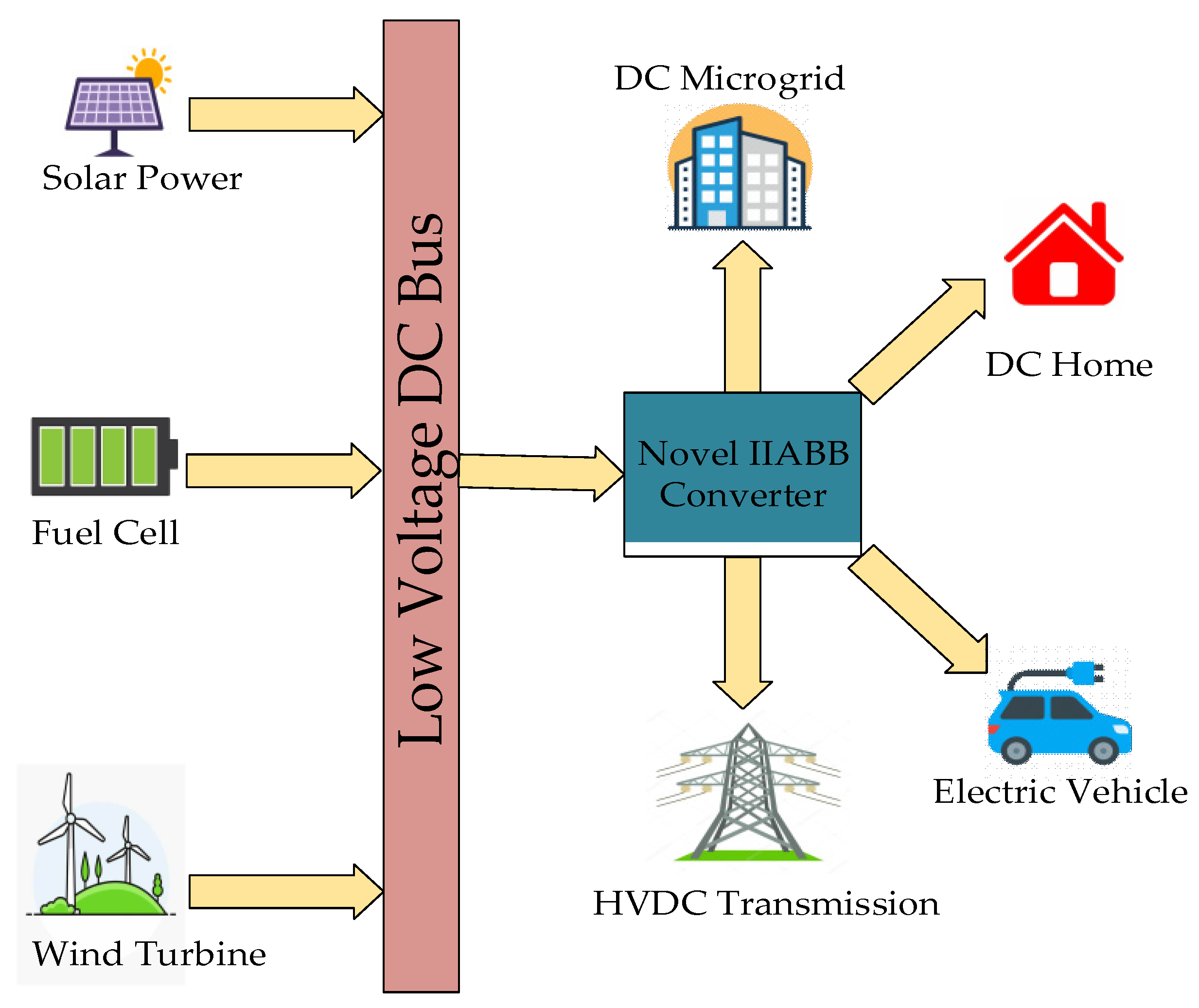
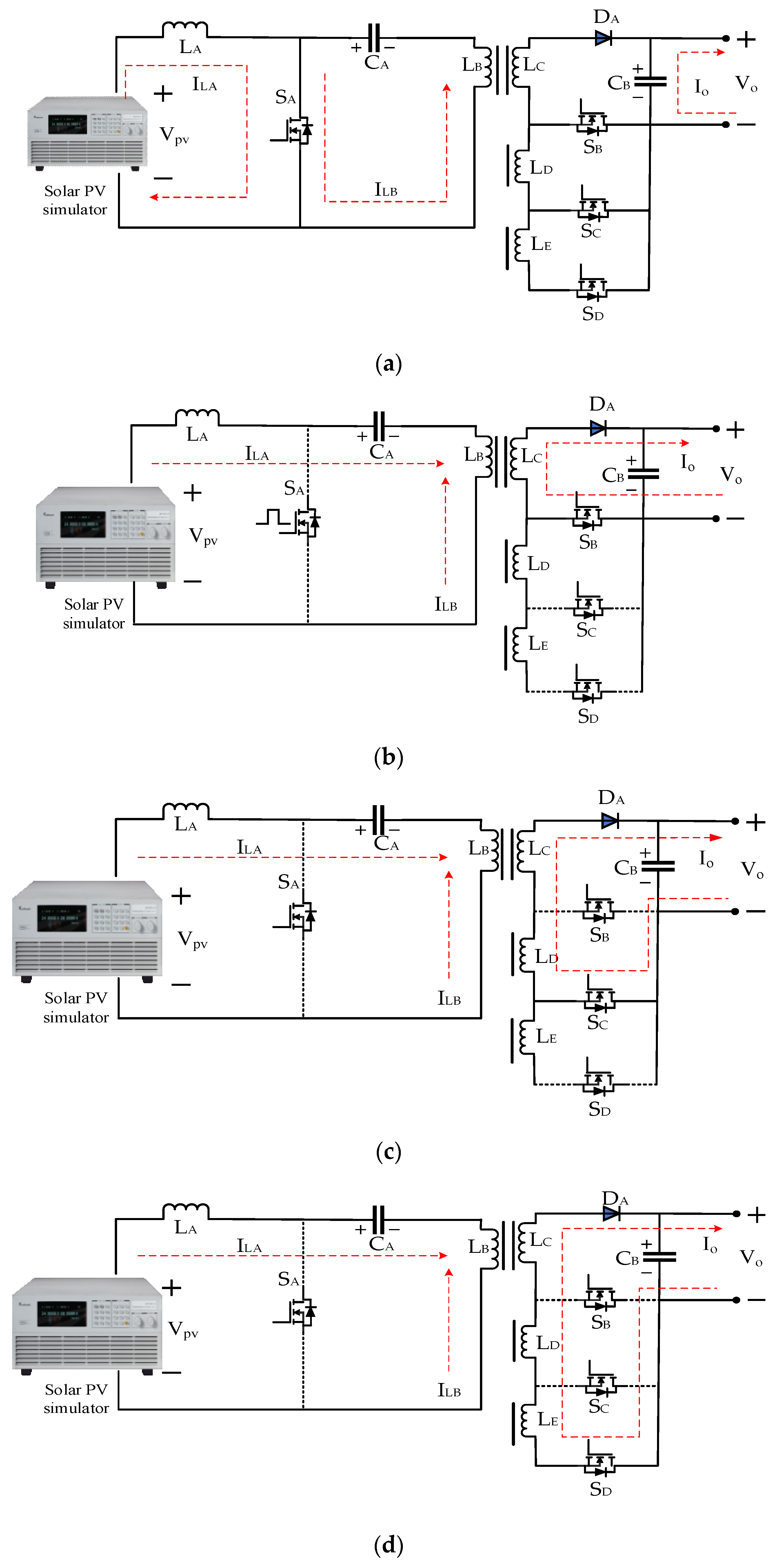
3. An Isolated Intelligent Adjustable Buck-Boost Converter Is Proposed

To increase the efficiency of the converter, a modified SEPIC converter is combined with five inductors; in this case, the five inductors are wound on the same core as the coupling design. To reduce ripple current and improve the system’s efficiency, and also considering that a high voltage or current can reduce the performance of the SEPIC converter. Five inductors (LA, LB, LC, LD, and LE) and four power MOSFETs (SA, SB, SC, and SD) are used in the proposed novel isolated intelligent adjustable buck-boost (IIABB) converter to adjust the applied voltage across the load side. Its advantage is that this IIABB converter has an intelligent control strategy so that the power MOSFETs (SB, SC, and SD) will not perform high-frequency switching caused by switching loss caused by those power MOSFETs (SB, SC, and SD) only for long ON or OFF times. As a result, the circuit has a different output power. To get the different output, further research can be performed on this design. In the proposed IIABB converter, the power MOSFET SA stores the output energy of the solar photovoltaic (PV) simulator in the inductor(s) LA, LB, LC, LD, and LE. When SA is ON, the inductor(s) LA, LB, LC, LD, and LE energy is transferred to the load side, which actuates the power MOSFETs SB, SC, and SD to further change the output voltage in order to stabilize the output power, as shown in Figure 4; the parameters for the proposed IIABB converter are given in Table 1.
The rising and falling of the output voltage of a conventional SEPIC converter depends on the duty cycle, the input voltage Vpv, the diode voltage VDA, the output voltage Vo, and the relationship between the number of connected inductors N and the turn ratio n (taking the turn ratio of 1:1) as expressed by Equation (5) below:
V o = D V pv V D A ( 1 D ) 1 D N · n
The circuit diagram of the proposed IIABB converter is shown in Figure 4. The solar PV simulator has an output voltage Vpv of 20 V, 30 V, and 40 V and a 48 V constant output voltage, which provides a consistent charging voltage for the various loads.

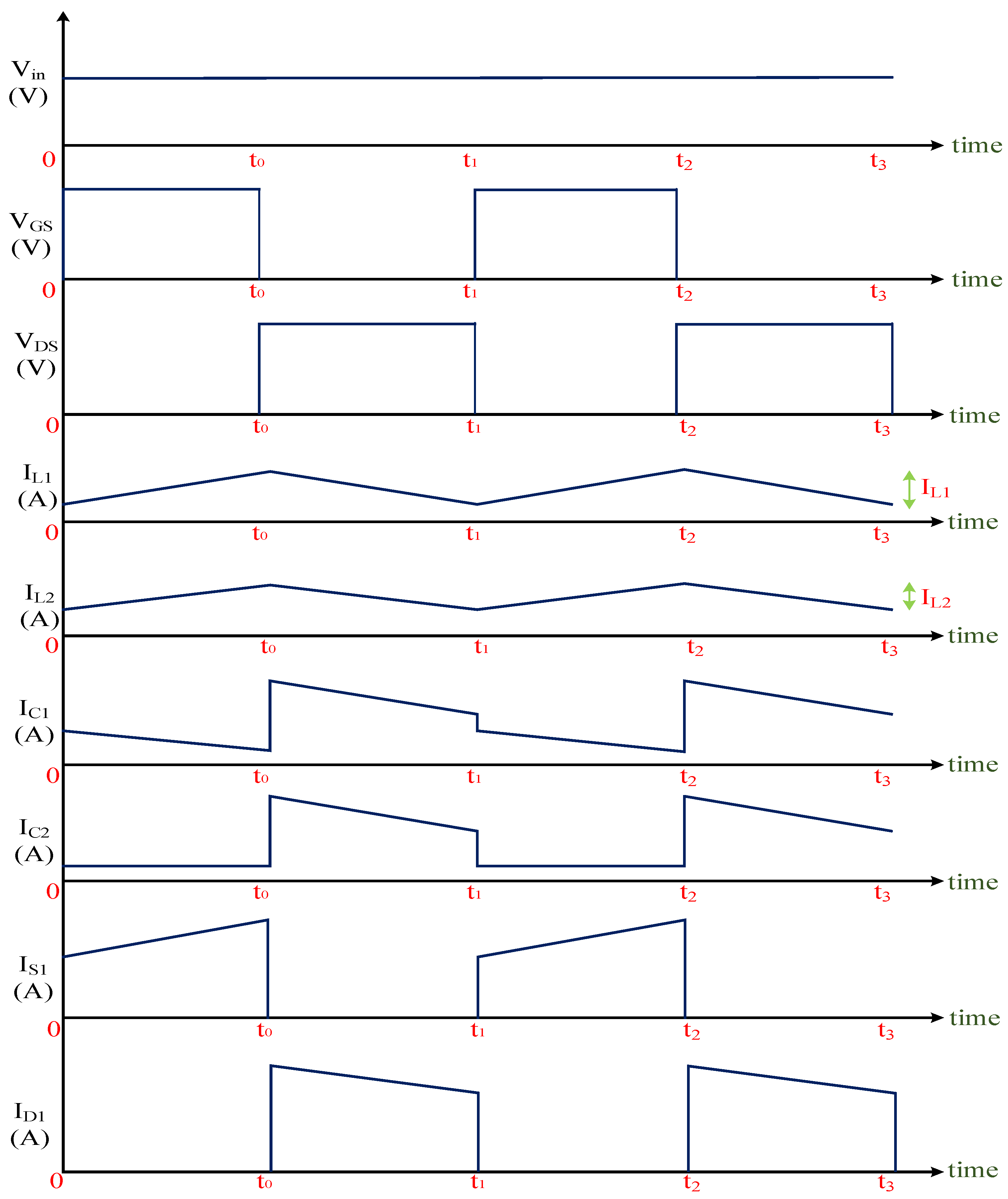
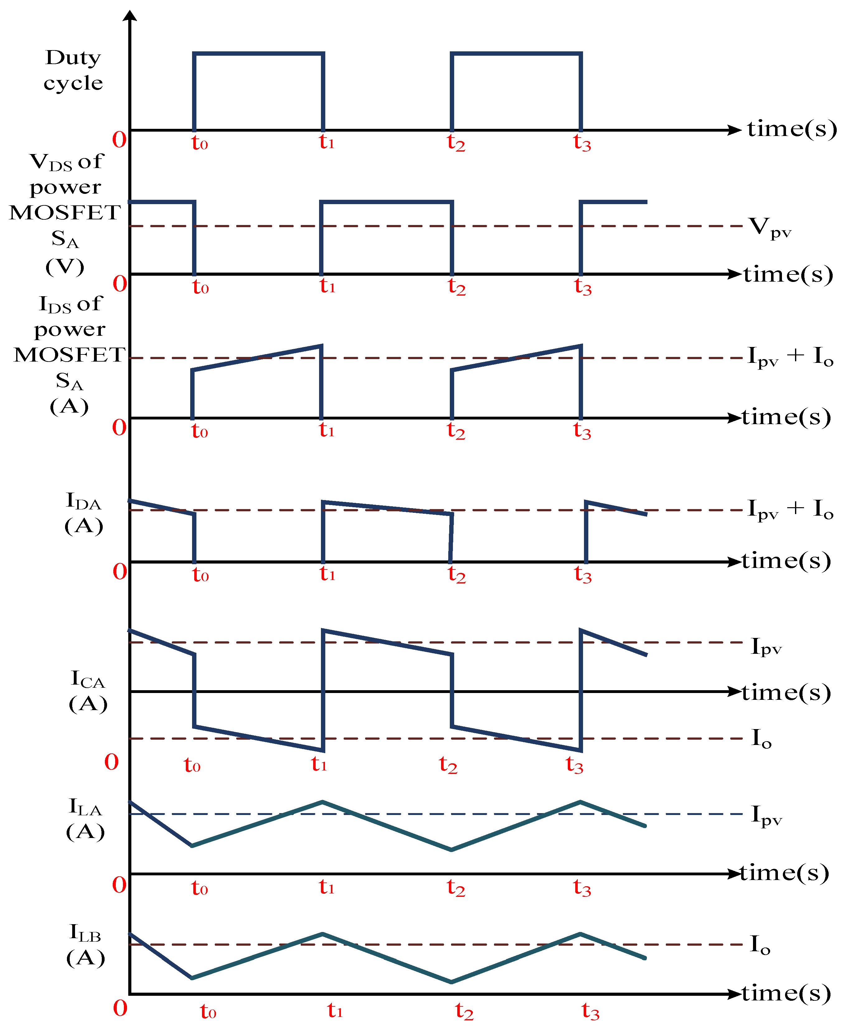
3.1. Topology Analysis and Intelligent Control Strategy

In this section, various modes of converter have been discussed at different conditions (mode 1, mode 2, and mode 3, respectively) at various duty cycles and numbers of inductors, which are calculated from the output gain Equation (5). The proposed IIABB converter has three working modes described below:
In mode 1 of the proposed IIABB converter combined with an intelligent control strategy, the switch SA is conducting and the output diode DA is reverse biased, and no currents will be conducting during this time. The magnetizing inductor LMA from inductor LA is subjected to a voltage, and its current rises according to Equation (6).
I LMA ( t ) =   V pv ( t 1 t 0 ) L MA + I LMA ( 0 )
The power MOSFET SA is ON and power MOSFETs SB, SC, and SD are OFF (as shown in Figure 4a), and the proposed IIABB converter operates according to the waveform during time t0–t1 as shown in Figure 5. In the next interval of the proposed IIABB converter, the power MOSFET SB is ON and the power MOSFETs SA, SC, and SD are OFF (as shown in Figure 4b), and the proposed IIABB converter operates according to the waveform during the time t1–t2, as shown in Figure 5. In mode 1, the Vo Equation (7) is as follows:
V o = D V pv V D A ( 1 D ) 1 D 1 · n
Equation (8) also applies to the magnetizing inductor LMB from inductor LB, whose current begins to increase when VCA is applied.
I LMB ( t ) =   V pv ( t 1 t 0 ) L MB + I LMB ( 0 )
It is during this mode that the load current is supplied by the output capacitor.
From the time t21–t2, the switch SA is not conducting a rectifying diode, and a coupled inductor will convert the energy stored in LMA and LMB into an output. According to Equations (9) and (10) below, the current on LMA and LMB will decrease when the voltage polarity is reversed on them.
I LMA ( t ) = I LMA ( t 1 ) V DS V CA L MA ( t 2 t 1 )
I LMB ( t ) = I LMB ( t 1 ) V DS V CA L MB ( t 2 t 1 )
One operating period ends, and a similar one begins in the time interval t2. Figure 5 illustrates the key waveforms of the proposed IIABB converter.
In mode 2, the power MOSFET SA is ON and the power MOSFETs SB, SC, and SD are OFF (as shown in Figure 4a), and the proposed IIABB converter operates according to the waveform during time t0–t1 as shown in Figure 5. In the next interval of the proposed IIABB converter, the power MOSFET SC is ON and the power MOSFETs SA, SB, and SD are OFF (as shown in Figure 4c), and the proposed IIABB converter operates according to the waveform during time t1–t2 as shown in Figure 5. The output voltage Vo can be calculated with the help of Equation (11) below:
V o = D V pv V D A ( 1 D ) 1 D 2 · n
Similarly, in mode 3, the power MOSFET SA is ON. The rest of the switches SB, SC, and SD are turned OFF (as shown in Figure 4a), and the proposed IIABB converter operates according to the waveform during time t0–t1 (Figure 5). In the next interval of the proposed IIABB converter, the power MOSFET SD is ON and the power MOSFETs SA, SB, and SC are OFF (as shown in Figure 4d), and the proposed IIABB converter operates according to the waveform during time t1–t2 (as shown in Figure 5). The output voltage Vo can be calculated with the help of Equation (12) below:
V o = D V pv V D A ( 1 D ) 1 D 3 · n

3.2. Topology Analysis

The proposed IIABB converter scheme is shown in Figure 4. The converter is at steady state, which implies that all currents and voltages are of a periodic nature, starting and ending at the same points over the whole switching period, and operating in current conduction mode (CCM).
The solar PV simulator output voltage Vpv and the DC blocking capacitor CA are considered constants. D is the duty ratio of the switch, DT is the period in which the switch is closed, and (1 − D)T is the period during which it is open.
Take ideal conditions into account: when the switch SA is open, the diode is ON, and Kirchhoff’s voltage law applies as follows:
VLA = Vpv
V CA V o N · n = 0
V CA = V o N · n
When the switch SA is closed, the diode is OFF. The voltage across LA for the interval DT is as follows:
V pv V LA V o N · n = 0
Kirchhoff’s voltage law around the path containing Vpv, VLA, and VCA gives the following:
V pv V LA + V CA V o N · n = 0
V LA = V pv + V CA V o N · n = 0
V LMA = V CA
V LMA = V o N · n
V pv D + ( V pv + V CA V o N · n ) ( 1 D ) = 0
V pv + V CA ( 1 D ) = V o N · n ( 1 D ) = 0
V CA ( 1 D ) + V o N · n ( 1 D ) 2 = 0
V CA ( 1 D ) + V o N · n · D ( 1 D ) 2 = 0
V CA ( 1 D ) = V o N · n · D ( 1 D ) 2
V pv V o N · n · D ( 1 D ) 2 = V o N · n · D ( 1 D )
V pv = V o N · n · D ( 1 D ) 2 + V o N · n · D ( 1 D )
V pv = V o ( 1 D ) 2 + V o ( 1 D ) N · n · D
V pv ( 1 D ) = V o ( 1 D ) + V o D N · n · D
Equation (30) for voltage gain switch voltage stress is as follows:
V o = D V pv 1 D N · n
where D is the duty cycle of the switch and ‘n’ is the turn ratio considered to be (1:1).

3.3. Hill-Climbing Algorithm

The hill-climbing (HC) algorithm is the MPPT algorithm often used in solar power systems. This is because of the HC algorithm’s simple control structure and low design cost. The HC algorithm is suitable for a uniform sunlight environment, and this algorithm is compared according to the output power of solar PV modules to control the actuating point and then catch the MPP. This algorithm’s disadvantages [25,26,27] are as follows:
(1)
With its disturbance characteristics, it will cause power loss and lower the system’s performance.
(2)
It is not suitable for partially shaded environments; it will operate at the local maximum power point, resulting in low system efficiency.
This study proposes an IIABB converter combined with the HC algorithm. The proposed IIABB converter is verified to be suitable for the MPPT algorithm under actual measurements so that the solar power generation system can capture MPP and improve system performance.

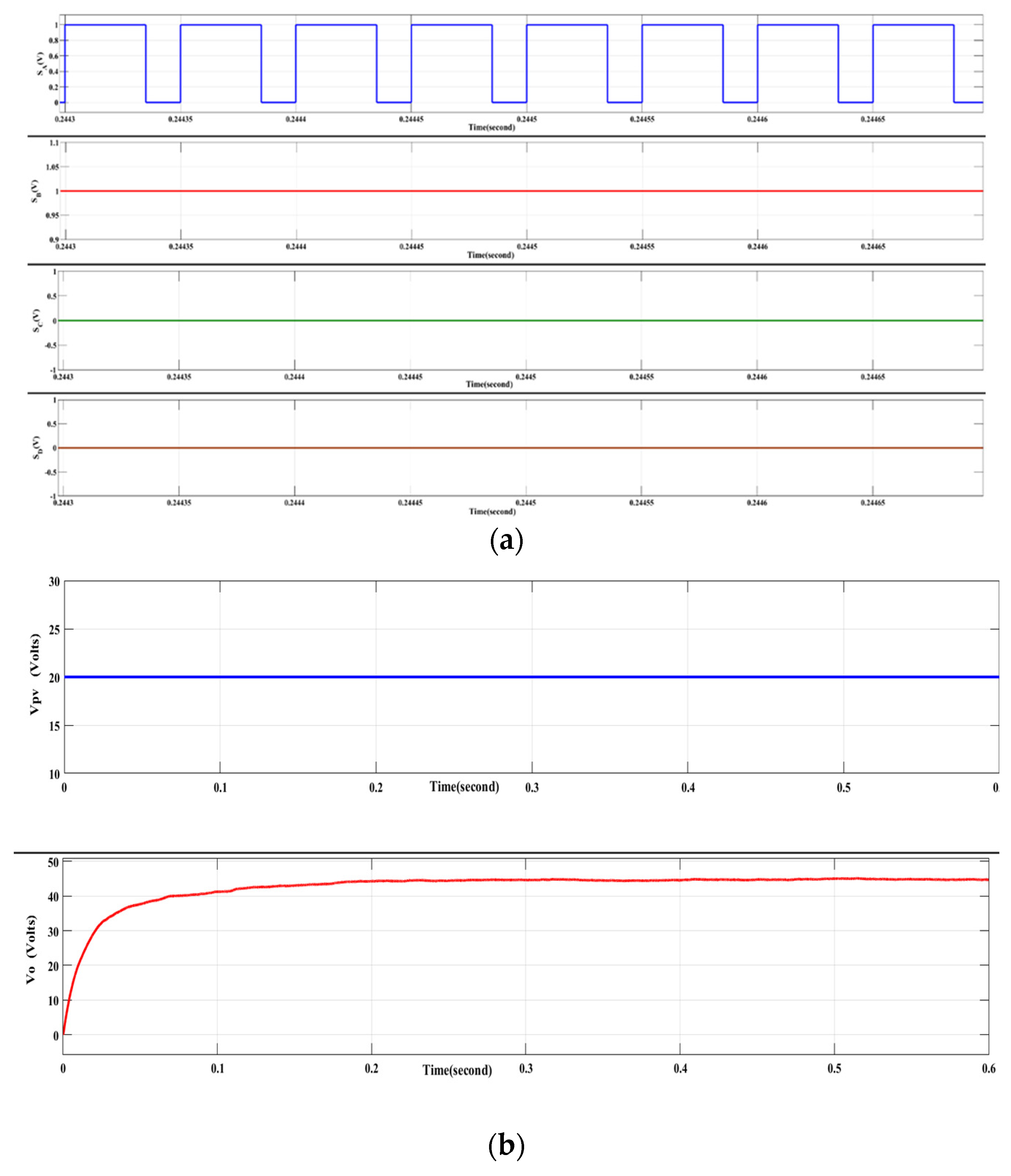
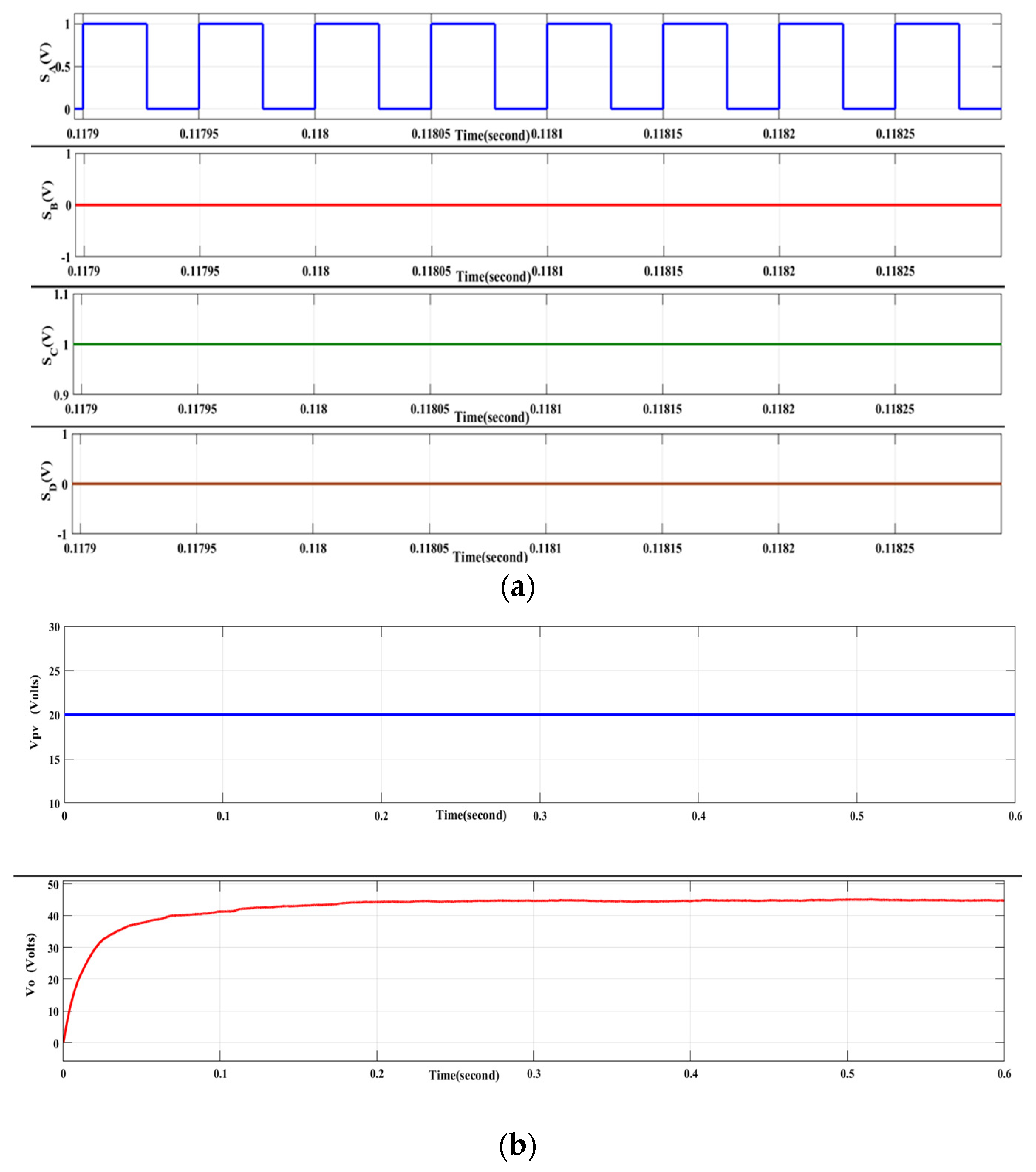
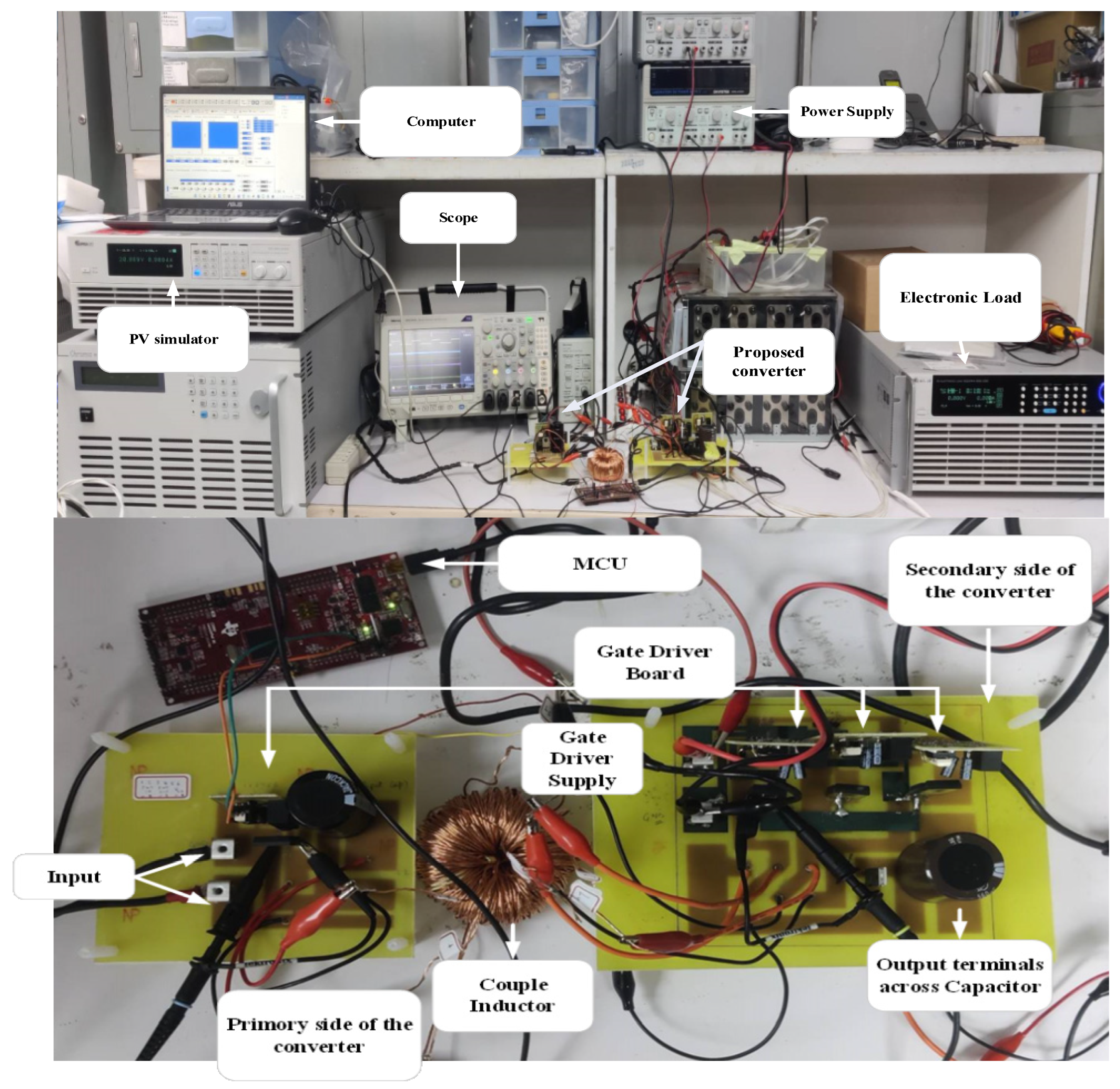
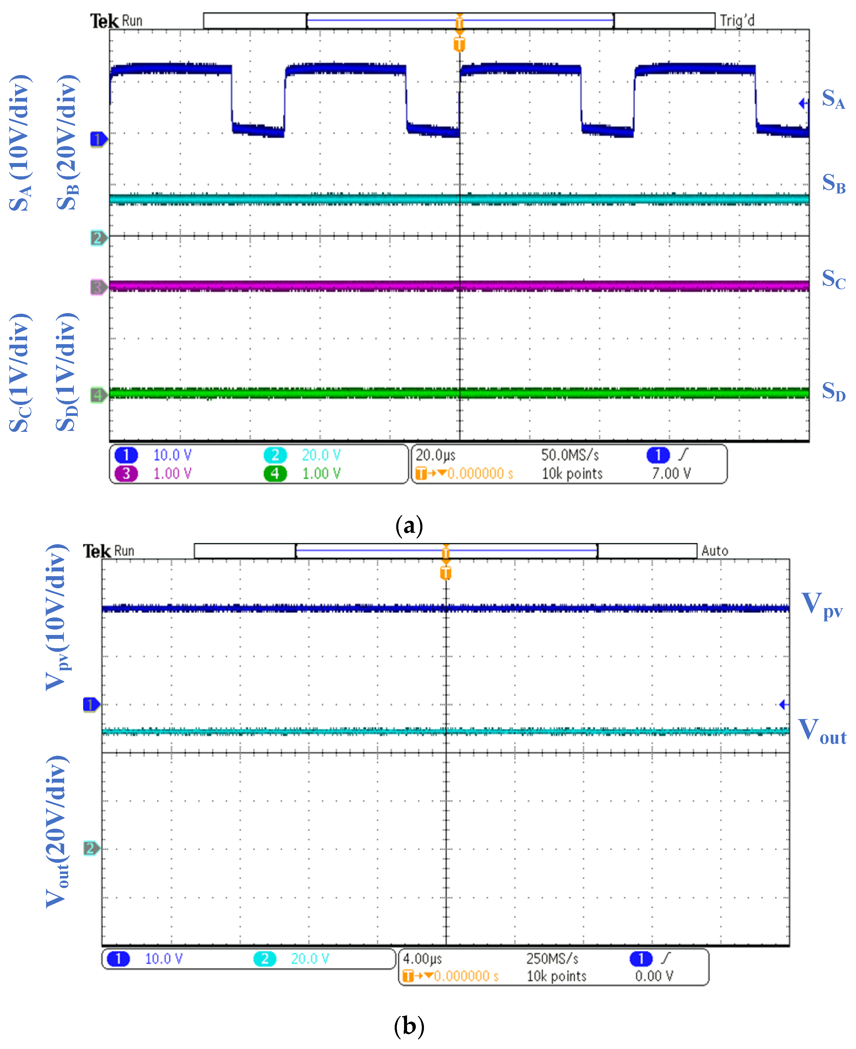
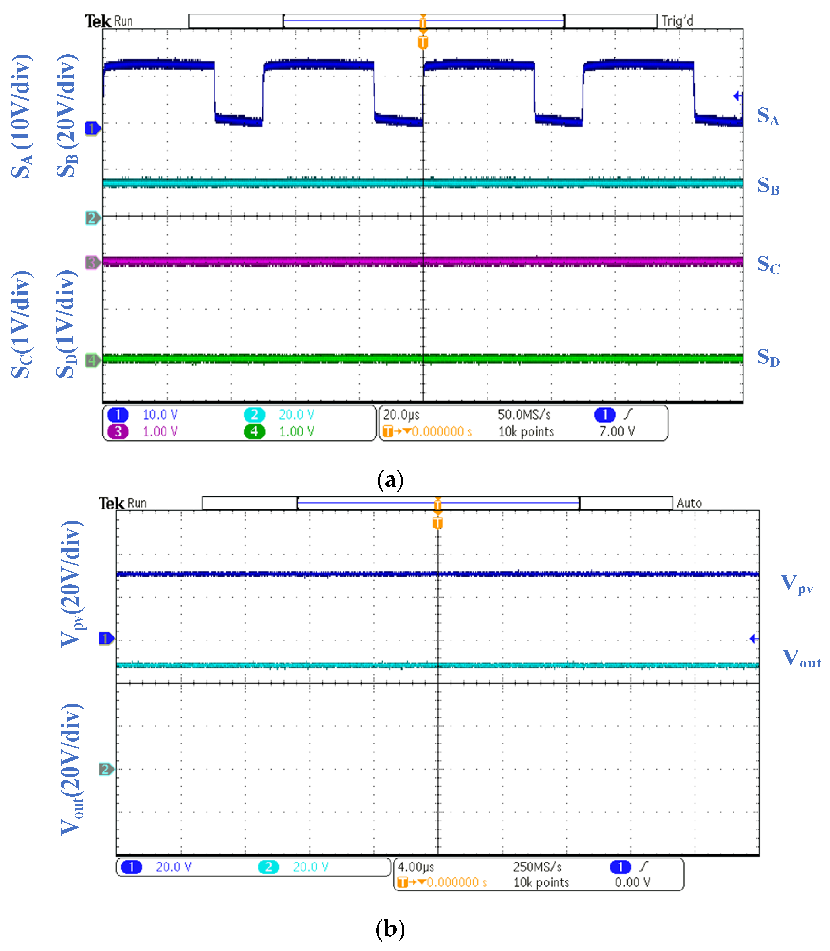
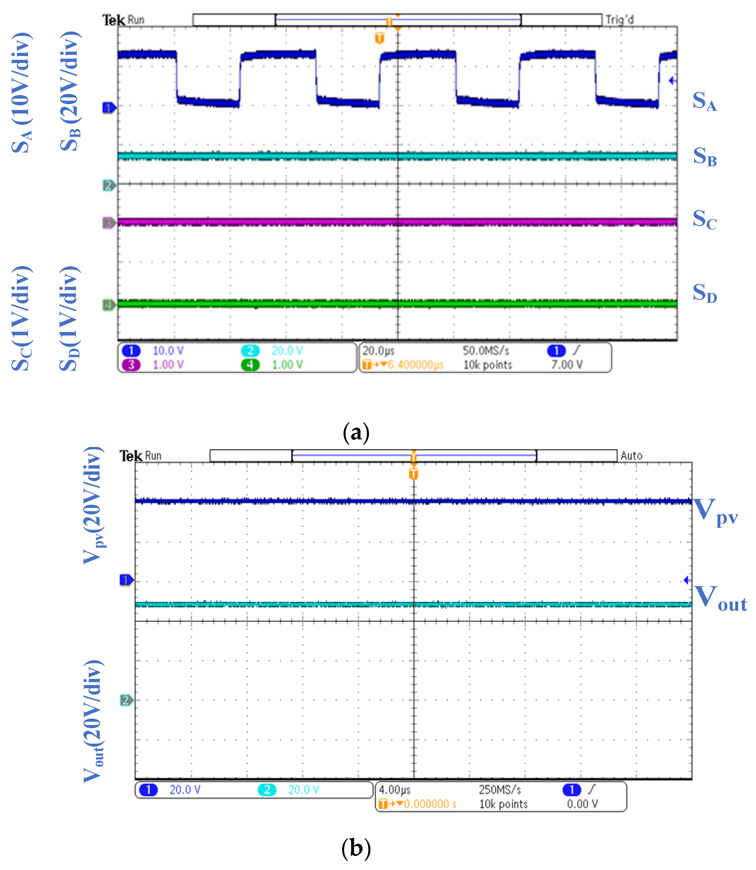
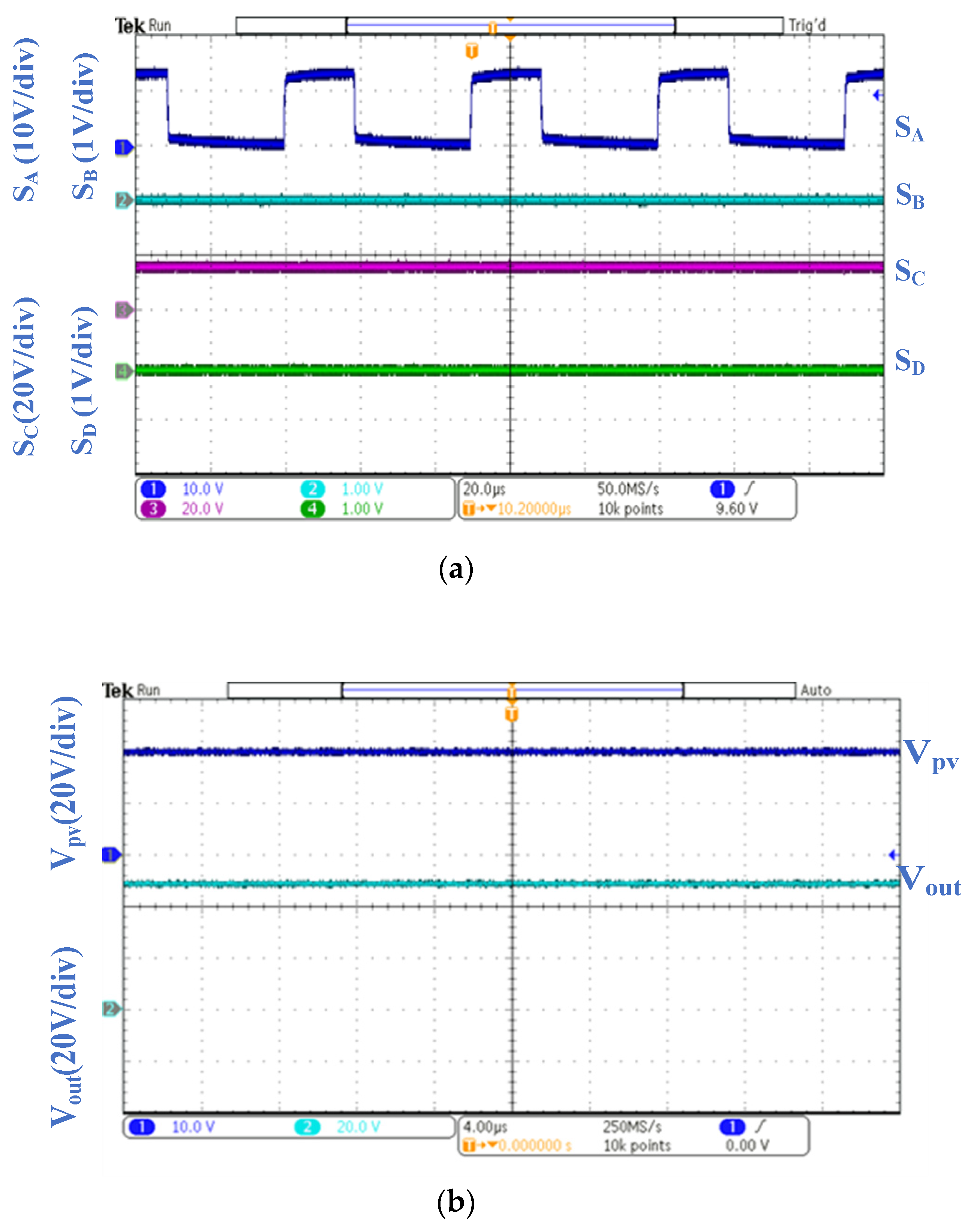
4. Simulation and Experimental Results

Simulation Result

The proposed IIABB converter is simulated in MATLAB R2021b at different input voltages, and the results are being compared with the conventional SEPIC converter. The parameters/components specifications used in MATLAB for the novel SEPIC converter are shown in Table 1. The proposed IIABB converter gives a constant output voltage Vo, irrespective of the solar PV module output voltage Vpv.
Some of the conditions are discussed below:
Condition 1:
Figure 6 shows the simulation waveform of the proposed IIABB converter for solar PV module output voltage Vpv of 20 V and N = 1. Figure 6a shows the switching modulation of the gate pulse of four switches by showing that switches SA and SB are in conduction mode whereas SC and SD are not conducting, and the duty cycle of the power MOSFET SA is calculated to be 0.7 by choosing the value of N = 1 with the help of Equation (7).
When the solar PV module output voltage of Vpv 20 V is applied with a duty cycle of 0.7, an output voltage of 48 V is achieved, as shown in Figure 6b for the use of battery charge.
Condition 2:
Figure 7 shows the simulation results of the proposed IIABB converter for Vpv of 20 V and N = 2. Figure 7a shows the switching modulation of the gate pulse of four switches with switches SA and SC in conduction mode, whereas SB and SD are not conducting, and the duty cycle of the power MOSFET SA is calculated to be 0.55 by choosing the value of N = 2 with the help of Equation (11). When Vpv = 20 V is applied with a duty cycle of 0.55, an output voltage of 48 V is achieved, as shown in Figure 7b for the use of battery charge.
Condition 3:
Figure 8 depicts the simulation results of the proposed IIABB converter for Vpv of 30 V and N = 3. Figure 8a shows the switching modulation of the gate pulse of four switches with switches SA and SD in conduction mode, whereas SB and SC are not conducting, and the duty cycle of the power MOSFET SA is calculated to be 0.35 by choosing the value of N = 3 with the help of Equation (12). When Vpv = 30 V is applied with a duty cycle of 0.35, an output voltage of 48 V is achieved, as shown in Figure 8b.
Table 2 illustrates the proposed topology compared with conventional SEPIC and boost converters, previous non-coupled inductor SEPIC-based converters [27,28], and other previous converters that employ the same topology. With reference to the other literature, this comparison compares the voltage gain capability of the proposed converter. It can be seen from the table that the voltage gain of the proposed converter is higher than those in [27,28,29] and also than the SEPIC and boost converters, both used in classical electronics. A continuous input current is also provided by the converter. Consequently, renewable energy applications will be easier to implement. Accordingly, the proposed converter has the advantages of coupled inductor converters and also has a high voltage gain, low voltage stress on the elements, a continuous input current, a positive output, and is capable of handling more power in comparison with the converters with near voltage gains in [28,30]. With the help of Table 2, it becomes clear that with a low duty ratio, the gain will be high and hence more efficient when compared to other topologies.
For the purpose of verifying the theoretical analysis and effectiveness of the proposed IIABB converter, a laboratory prototype of the converter is implemented and tested in conjunction with the previous section. The proposed IIABB converter specification is shown in Table 1. The above simulation results were verified by hardware implementation. Figure 9 illustrates the experimental setup of the proposed converter. For controlling the novel converter, the Texas DSP TMS320F28379D is used as a pulse width modulation IC. In Table 3, the solar PV simulator specifications are under an irradiance level of 1000 W/m2 and a temperature of 25 °C; we have taken 50 V and 5.5 A for the open circuit voltage and short circuit current, respectively, and 200 W as the maximum power achieved.
Table 4 illustrates the hardware results for the proposed IIABB converter by varying the number of inductors (N) along with the solar PV simulator output voltage Vpv and the constant output voltage variation because a battery charger requires constant output voltage with various advantages. As the number of inductors increases, the current ripple of the proposed converter reduces, providing high gain with a low duty ratio when compared to a conventional SEPIC converter. Moreover, the coupled inductor reduces the size of the whole circuitry.
Figure 10 shows the experimental waveform of the proposed IIABB converter for a Vpv of 20 V and number of inductors N = 1. Figure 11a displays the switches SA and SB are operating, while SC and SD are not operating, and the switches work via an intelligent control strategy. Figure 11b shows the waveform of Vpv = 20 V and an output voltage of Vout = 48 V at a duty cycle of 0.7 according to Equation (5). Figure 11 shows the experimental waveform of the proposed IIABB converter for a Vpv of 30 V and N = 1. Figure 12a displays the switches SA and SB are operating; the switches SC and SD are not operating via an intelligent control strategy. Figure 12b shows the waveform of Vpv = 20 V and an output voltage of Vout = 48 V at a duty cycle of 0.62 according to Equation (5), as shown in Table 4.
Figure 12, Figure 13 and Figure 14 show an irradiance level of 1000 W/m2 and a temperature of 25 °C, the experimental waveform of the proposed IIABB converter, and N = 1, 2, and 3, respectively. In these cases, the proposed IIABB converter has an intelligent control strategy and HC algorithm. First, switch SA works by the HC algorithm. Second, switches SB, SC, and SD work via an intelligent control strategy. Finally, Vpv = 40 V, i.e., the HC algorithm, catches the maximum power point voltage Vmpp, and Vout = 48 V can offer battery charging, as shown in Table 4.

5. Conclusions

This study has presented a detailed description and circuit design, as well as step-by-step design equations for the proposed IIABB converter for a solar power system. The proposed converter has a constant output voltage and can be utilized with an intelligent control strategy and HC MPPT algorithm to capture the MPP. With the help of MATLAB R2021, the performance of the innovative IIABB converter is compared and verified with the performance of the conventional SEPIC converter. Instead of a transformer, a coupled inductor is designed, which significantly reduces the input current ripple of the converter and hence reduces the cost and size of the converter. Simulation results and experimental results revealed that the proposed converter is more efficient than conventional DC–DC converters at various input voltage levels and gives high efficiency at low duty cycles. In addition, we use the HC algorithm for MPPT control, which improves the system’s performance. The proposed IIABB converter efficiency is ~92–99%. In this case, we have taken an electronic load in CC (constant current) mode. When the load changes, the load current will change, and output can control voltage level from the load terminal.
This research has contributed to the development of a novel IIABB converter that may be employed in renewable energy systems. The constant output voltage of the novel converter can be used for battery charging and for inverter applications; therefore, the proposed converter is suitable for various conditions.
In the future, we can increase the number of components in the proposed IIABB converter so that it can be used for high-power applications, such as for large industrial purposes and numerous PV applications; moreover, by making some minor changes in the circuitry, a new form of DC–AC inverter can also be proposed with the help of this same idea.

Author Contributions

Conceptualization, B.S., H.-D.L. and C.-H.L.; Formal analysis, B.S. and H.-D.L.; Investigation, B.S. and H.-D.L.; Methodology, B.S., H.-D.L. and C.-H.L.; Supervision, H.-D.L.; Writing—original draft, B.S., H.-D.L., C.-H.L., S.-D.L., A.S. and L.-Y.H.; Writing—review & editing, B.S., H.-D.L., C.-H.L., S.-D.L., A.S. and L.-Y.H. All authors provided critical feedback and helped with the research and analysis of the manuscript. All authors have read and agreed to the published version of the manuscript.

Funding

This research was funded by the National Science and Technology Council, Taiwan, R.O.C., grant number MOST 111-2221-E-003-012. This work was also supported by the National Taiwan Normal University Subsidy Policy for International Collaboration and Research Projects and the Innovation-Oriented Trilateral Proposal for Young Investigators of NTU SYSTEM.

Data Availability Statement

Not applicable.

Conflicts of Interest

The authors declare no conflict of interest.

References

  1. Meena Devi, R.; Geetha, V.; Meenakshi, V. Speed Control of SEPIC Converter-Based Induction Motor Drive System. In Emerging Solutions for e-Mobility and Smart Grids; Springer: Singapore, 2021; pp. 15–23. [Google Scholar] [CrossRef]
  2. Nguimfack-Ndongmo, J.D.D.; Kenné, G.; Kuate-Fochie, R.; Tchouani Njomo, A.F.; Mbaka Nfah, E. Adaptive neuro-synergetic control technique for SEPIC converter in PV systems. Int. J. Dyn. Control 2022, 10, 203–216. [Google Scholar] [CrossRef]
  3. Sivamani, D.; Ramkumar, R.; Ali, A.N.; Shyam, D. Design and implementation of highly efficient UPS charging system with single-stage power factor correction using SEPIC converter. Mater. Today Proc. 2021, 45, 1809–1819. [Google Scholar] [CrossRef]
  4. Faizan, M.; Sabir, B.; Tahir, M.; Rahman, K.; Ashraf, I. Analysis of Five Level H-Bridge Inverter Using Bipolar Switching Schemes. In Proceedings of the 2021 International Conference on Computer Communication and Informatics (ICCCI), Coimbatore, India, 27–29 January 2021; pp. 1–6. [Google Scholar] [CrossRef]
  5. Maroti, P.K.; Padmanaban, S.; Holm-Nielsen, J.B.; Bhaskar, M.S.; Meraj, M.; Iqbal, A. A new structure of high voltage gain SEPIC converter for renewable energy applications. IEEE Access 2019, 7, 89857–89868. [Google Scholar] [CrossRef]
  6. Maroti, P.K.; Esmaeili, S.; Iqbal, A.; Meraj, M. High step-up single switch quadratic modified SEPIC converter for DC microgrid applications. IET Power Electron. 2020, 13, 3717–3726. [Google Scholar] [CrossRef]
  7. Mosconi Ewerling, M.V.; Brunelli Lazzarin, T.; Illa Font, C.H. Proposal of an Isolated Two-Switch DC-DC SEPIC Converter. In Proceedings of the 2019 IEEE 15th Brazilian Power Electronics Conference and 5th IEEE Southern Power Electronics Conference (COBEP/SPEC), Santos, Brazil, 1–4 December 2019; pp. 1–6. [Google Scholar] [CrossRef]
  8. Natchimuthu, S.; Chinnusamy, M.; Mark, A.P. Experimental investigation of PV based modified SEPIC converter fed hybrid electric vehicle (PV-HEV). Int. J. Circ. Theor. Appl. 2020, 48, 980–996. [Google Scholar] [CrossRef]
  9. Majstorović, M.; Mršević, D.; Đurić, B.; Milešević, M.; Stević, Z.; Despotović, Ž.V. Implementation of MPPT Methods with SEPIC Converter. In Proceedings of the 2020 19th International Symposium INFOTEH-JAHORINA (INFOTEH), East Sarajevo, Bosnia and Herzegovina, 18–20 March 2020; pp. 1–6. [Google Scholar] [CrossRef]
  10. Mouslim, S.; Kourchi, M.; Ajaamoum, M. Simulation and analyses of SEPIC converter using linear PID and fuzzy logic controller. Mater. Today Proc. 2020, 27, 3199–3208. [Google Scholar] [CrossRef]
  11. Kravetz, F.I.; Gules, R. Soft-Switching High Static Gain Modified SEPIC Converter. IEEE J. Emerg. Sel. Top. Power Electron. 2021, 9, 6739–6747. [Google Scholar] [CrossRef]
  12. Sivaramkrishnan, M.; Marthanda, A.V.G.A.; Prasad, K.L.; Mujeer, S.A.; Durairaj, U.; Salim, M. Simulation of PV and WECS using CUK and SEPIC converter. In Proceedings of the 2021 5th International Conference on Intelligent Computing and Control Systems (ICICCS), Madurai, India, 6–8 May 2021; pp. 1–7. [Google Scholar] [CrossRef]
  13. Kumari, R.; Pandit, M.; Sherpa, K. Modelling and Comparison of Conventional SEPIC Converter with Cascaded Boost–SEPIC Converter. J. Inst. Eng. India Ser. B 2021, 102, 99–109. [Google Scholar] [CrossRef]
  14. Lu, S.-D.; Lin, C.-H.; Huang, L.-Y.; Lee, Y.-L.; Liu, H.-D.; Liao, P.-C.; Gao, G.-J.; Hsu, C.-M. Novel Global-MPPT Control Strategy Considering the Variation in the Photovoltaic Module Output Power and Loads for Solar Power Systems. Processes 2022, 10, 367. [Google Scholar] [CrossRef]
  15. Balaji, C.; Anuradha, C.; Chellammal, N.; Bharadwaj, R. An extendable high-efficiency triple-port SEPIC–SEPIC converter with continuous input currents for DC microgrid applications. Int. Trans. Electr. Energy Syst. 2021, 31, e13121. [Google Scholar] [CrossRef]
  16. Alili, A.; Camara, M.B.; Dakyo, B. Vienna Rectifier-Based Control of a PMSG Wind Turbine Generator. Processes 2022, 10, 413. [Google Scholar] [CrossRef]
  17. Zunnurain, I.A.; Yumi, K.M.; Faisal, M.H. Performance Analysis of Single-Phase Inverter Using SEPIC Converter. In Proceedings of the 6th International Conference on Electrical, Control and Computer Engineering; Md. Zain, Z., Sulaiman, M.H., Mohamed, A.I., Bakar, M.S., Ramli, M.S., Eds.; Lecture Notes in Electrical Engineering; Springer: Singapore, 2022; Volume 842. [Google Scholar] [CrossRef]
  18. Ghamari, S.M.; Gholizadeh-Narm, H.; Khavari, F. Robust Adaptive Controller Design for DC-DC SEPIC Converter in Photo Voltaic Application. In Proceedings of the 2019 6th International Conference on Control, Instrumentation and Automation (ICCIA), Sanandaj, Iran, 30–31 October 2019; pp. 1–6. [Google Scholar] [CrossRef]
  19. Islam, N.; Mohammad, K.; Khan, R.A.; Sarwer, Z.; Sarwar, A. Symmetrical and Asymmetrical Multilevel Inverter Topologies with Reduced Device Count: A Review. In Proceedings of the 2nd International Conference for Emerging Technology (INCET), Belagavi, India, 21–23 May 2021; pp. 1–6. [Google Scholar] [CrossRef]
  20. Yadav, A.; Verma, A. Modeling and Analysis of Modified SEPIC Converter Fed by Solar PV System. In Proceedings of the 2nd International Conference on Advances in Computing, Communication Control and Networking, Greater Noida, India, 18–19 December 2020; pp. 633–638. [Google Scholar] [CrossRef]
  21. Nowdeh, S.A.; Moghaddam, M.J.H.; Babanezhad, M.; Davoodkhani, I.F.; Kalam, A.; Ahmadi, A.; Abdelaziz, A.Y. A novel maximum power point tracking method for photovoltaic application using secant incremental gradient based on Newton Raphson. In Solar Photovoltaic Power Plants: Advanced Control and Optimization Techniques; Springer: Singapore, 2019; pp. 71–96. [Google Scholar]
  22. Arabi Nowdeh, S.; Moghaddam, M.J.H.; Nasri, S.; Abdelaziz, A.Y.; Ghanbari, M.; Faraji, I. A new hybrid moth flame optimizer-perturb and observe method for maximum power point tracking in photovoltaic energy system. In Modern Maximum Power Point Tracking Techniques for Photovoltaic Energy Systems; Springer: Cham, Switzerland, 2020; pp. 401–420. [Google Scholar]
  23. Davoodkhani, F.; Nowdeh, S.A.; Abdelaziz, A.Y.; Mansoori, S.; Nasri, S.; Alijani, M. A New Hybrid Method Based on Gray Wolf Optimizer-Crow Search Algorithm for Maximum Power Point Tracking of Photovoltaic Energy System. In Modern Maximum Power Point Tracking Techniques for Photovoltaic Energy Systems; Springer: Cham, Switzerland, 2019; pp. 421–438. [Google Scholar]
  24. Nasri, S.; Nowdeh, S.A.; Davoudkhani, I.F.; Moghaddam, M.J.H.; Kalam, A.; Shahrokhi, S.; Zand, M. Maximum power point tracking of photovoltaic renewable energy system using a new method based on turbulent flow of water-based optimization (TFWO) under Partial Shading Conditions. In Fundamentals and Innovations in Solar Energy; Springer: Singapore, 2021; pp. 285–310. [Google Scholar]
  25. Lee, Y.-L.; Liu, H.-D. A Novel MPPT Heating Control Strategy Applied to the Induction Heating System. Processes 2022, 10, 1151. [Google Scholar] [CrossRef]
  26. Liu, H.-D.; Lu, S.-D.; Lee, Y.-L.; Lin, C.-H. A Novel Photovoltaic Module Quick Regulate MPPT Algorithm for Uniform Irradiation and Partial Shading Conditions. Processes 2021, 9, 2213. [Google Scholar] [CrossRef]
  27. Gules, R.; Santos, W.M.D.; Reis, F.A.D.; Romaneli, E.F.R.; Badin, A.A. A modified SEPIC converter with high static gain for renewable applications. IEEE Trans. Power Electron. 2014, 29, 5860–5871. [Google Scholar] [CrossRef]
  28. Banaei, M.R.; Sani, S.G. Analysis and implementation of a new SEPIC-based single switch buck-boost dc-dc converter with continuous input current. IEEE Trans. Power Electron. 2018, 33, 10317–10325. [Google Scholar] [CrossRef]
  29. Banaei, M.R.; Ardi, H.; Farakhor, A. Analysis and implementation of a new single-switch buck–boost DC/DC converter. IET Power Electron. 2014, 7, 1906–1914. [Google Scholar] [CrossRef] [Green Version]
  30. Banaei, M.R.; Bonab, H.A.F. A novel structure for singleswitch nonisolated transformerless buck–boost DC–DC converter. IEEE Trans. Ind. Electron. 2017, 64, 198–205. [Google Scholar] [CrossRef]
Figure 1. Various applications of the novel IIABB converter.
Processes 11 01010 g001
Figure 2. SEPIC Converter’s operate mode: (a) power MOSFET S1 during the ON state, (b) power MOSFET S1 during the OFF state.
Processes 11 01010 g002
Figure 3. Current and voltage waveforms of a conventional SEPIC converter.
Processes 11 01010 g003
Figure 4. Operation of the proposed IIABB converter with an intelligent control strategy: (a) the power MOSFET SA is ON and the power MOSFETs SB, SC, and SD are OFF, (b) the power MOSFET SB is ON and the power MOSFETs SA, SC, and SD are OFF, (c) the power MOSFET SC is ON and the power MOSFETs SA, SB, and SD are OFF, and (d) the power MOSFET SD is ON and the power MOSFETs SA, SB, and SC are OFF.
Processes 11 01010 g004
Figure 5. Voltage and current waveforms show VDS, IDS, IDA, ICA, ILA, and ILB along with the duty cycle of the proposed IIABB converter.
Processes 11 01010 g005
Figure 6. Simulation result of the proposed IIABB converter for solar PV module input voltage Vpv of 20 V and corresponding output voltage Vo = 48 V and number of connected inductors N = 1 with duty cycle 0.7 (a) gate pulse waveform where SA and SB are in operating condition and SC and SD are not operating, and (b) the Vpv and output voltage Vo.
Processes 11 01010 g006
Figure 7. Simulation result of the proposed IIABB converter for solar PV module input voltage Vpv of 20 V and corresponding output voltage Vo = 48 V and number of connected inductors N = 2 with duty cycle 0.55 (a) gate pulse waveform where SA and SC are in operating condition and SB and SD are not operating, and (b) the Vpv and output voltage Vo.
Processes 11 01010 g007
Figure 8. Simulation result of the proposed IIABB converter for solar PV module input voltage Vpv of 30 V and corresponding output voltage Vo = 48 V and number of connected inductors N = 3 with duty cycle 0.35 (a) gate pulse waveform where SA and SD are in operating condition and SB and SC are not operating, and (b) the Vpv and output voltage Vo.
Processes 11 01010 g008
Figure 9. Hardware prototype of the proposed IIABB converter.
Processes 11 01010 g009
Figure 10. Experimental waveforms of the proposed IIABB converter for Vpv of 20 V and N = 1: (a) experimental waveforms of switches SA and SB are operating; SC and SD are not operating; and (b) waveforms of Vpv = 20 V and output voltage Vout = 48 V via an intelligent control strategy at a duty cycle of 0.7.
Processes 11 01010 g010
Figure 11. Experimental waveforms of the proposed IIABB converter for Vpv of 30 V and N = 1: (a) experimental waveforms of switches SA and SB that are operating; SC and SD are not operating; and (b) waveforms of Vpv = 30 V and output voltage Vout = 48 V via an intelligent control strategy at a duty cycle of 0.62.
Processes 11 01010 g011
Figure 12. Experimental waveforms of the proposed IIABB converter for Vpv of 40 V and N = 1: (a) experimental waveforms of switches SA and SB are operating; SC and SD are not operating; and (b) waveforms of Vpv = 40 V and output voltage Vout = 48 V via an intelligent control strategy and HC MPPT algorithm at a duty cycle of 0.55.
Processes 11 01010 g012
Figure 13. Experimental waveforms of the proposed IIABB converter for Vpv of 40 V and N = 2: (a) experimental waveforms of switches SA and SC are operating; SB and SD are not operating; and (b) waveforms of Vpv = 40 V and output voltage Vout = 48 V via an intelligent control strategy and HC MPPT algorithm at a duty cycle of 0.38.
Processes 11 01010 g013
Figure 14. Experimental waveforms of the proposed IIABB converter for Vpv of 40 V and N = 3: (a) experimental waveforms of switches SA and SD are operating; SB and SC are not operating; and (b) waveforms of Vpv = 40 V and output voltage Vout = 48 V via an intelligent control strategy and HC MPPT algorithm at a duty cycle of 0.3.
Processes 11 01010 g014
Table 1. The parameters of the proposed IIABB converter.
Component/ParameterSpecificationQuantity
Solar PV simulator output voltage (Vpv)20–40 V--
Switching frequency20 kHz--
Rated power200 W--
Capacitor (CA, CB)220 µF, 500 µF2
Inductors (LA, LB, LC, LD, LE)1 mH5
Output voltage (Vo)48 V--
Table 2. Comparison between the proposed converter and some other converters.
ReferencesParameters
Voltage GainNumber of SwitchesNumber of DiodesNumber of InductorsContinous Input Current
Proposed D V pv 1 D N · n 425Yes
SEPIC D 1 D 122Yes
Boost D 1 D 111Yes
[27] 1 + D 1 D 122Yes
[28] 3 D 1 D 122Yes
[29] 2 D 1 D 122No
[30] 3 D 1 D 133No
Table 3. The solar PV simulator specification.
ParametersSpecification
Open circuit voltage (Voc)50 V
Short circuit current (Isc)5.5 A
Maximum power point voltage (Vmpp)40 V
Maximum power point current (Impp)5 A
Maximum power point (Pmpp)200 W
Table 4. Hardware results for the proposed IIABB converter for battery charger application.
Number of InductorsVpvVoDEfficiency
N = 120 V48 V0.7092%
30 V48 V0.6294%
40 V48 V0.5596%
N = 220 V48 V0.5596%
30 V48 V0.4798%
40 V48 V0.3899%
N = 320 V48 V0.4598%
30 V48 V0.3599%
40 V48 V0.3099%
Disclaimer/Publisher’s Note: The statements, opinions and data contained in all publications are solely those of the individual author(s) and contributor(s) and not of MDPI and/or the editor(s). MDPI and/or the editor(s) disclaim responsibility for any injury to people or property resulting from any ideas, methods, instructions or products referred to in the content.

