Article

Numerical Analysis and Structure Optimization of Concentric GST Ring Resonator Mounted over SiO2 Substrate and Cr Ground Layer

1
Department of Electrical Engineering, College of Engineering, Jouf University, Sakaka 72388, Saudi Arabia
2
Department of Information and Communication Technology, Marwadi University, Rajkot 360003, India
3
Department of Electrical Engineering, Marwadi University, Rajkot 360003, India
4
Department of Computer Engineering, Marwadi University, Rajkot 360003, India
*
Authors to whom correspondence should be addressed.
Mathematics 2023, 11(5), 1257; https://doi.org/10.3390/math11051257
Submission received: 13 February 2023 / Revised: 28 February 2023 / Accepted: 2 March 2023 / Published: 5 March 2023
(This article belongs to the Special Issue Computational Methods and Applications for Numerical Analysis)

Abstract

:
Since the introduction of Metal-Insulator-Metal (MIM) absorbers, most of the structures demonstrated a narrowband absorption response which is not suitable for potential applications in photovoltaic systems, as it requires higher energy to enhance its performance. Very little research is being conducted in this direction; to address this issue, we exhibit a broadband solar absorber designed using a concentric GST ring resonator placed upon a silicon dioxide substrate layer with chromium used as a ground plane. It was analyzed using the finite element method. The design is also optimized by using a nonlinear parametric optimization algorithm. Comparatively less work has been focused on solar absorbers designed with the help of GST material, and here we have compared the effect of two different phases of GST, i.e., amorphous (aGST) and crystalline (cGST); the results indicate the higher performance of aGST phase. Parametric optimization has been adapted to identify the optimal design to attain high performance at minimal resources. The absorption response is angle insensitive for 0 to 60 degrees, and at the same time for both TE and TM modes, the design provides identical results, indicating the polarization-insensitive properties. The electric field intensity changes at the six peak wavelengths are also demonstrated for the authentication of the high performance. Thus, the proposed concentric GST ring resonator solar absorber can present a higher solar energy absorption rate than other solar structure designs. This design can be applied for improving the performance of photovoltaic systems.

1. Introduction

Nowadays, many appliances are used to ease our daily lives, but the power supplies for these appliances need to be considered, as they contribute significantly towards the major issues of climate change and global warming. To solve this problem, solar energy plays an important role [1]. Photonics defines the technology of light, and the main function of photonic technology is to encompass generating, manipulating, amplifying, guiding, and detecting light [2]. Moreover, it can be used in our phones, such as lasers, cameras, optical fibers, and screens. Optical tweezers and lighting are also used in cars, homes, TVs, and computers [3]. Photonic devices are used in the medical field and for a large generation of power in the industrial field [4]. Photonic devices play an important role in our daily lives; therefore, by studying photonic technology, we can improve many other science fields, such as optical, microwave, wireless communication, solar energy systems, and so on [5]. One of the main reasons to develop the solar energy system is to reduce the damage to our natural environment and stop the toxic gases produced by large industries [6]. The solar energy system intends to reduce the greenhouse effect we have been facing for the last decade [7]. Several numerical algorithms have also been employed for photovoltaic cell analysis [8,9].
Engineers have developed many techniques to improve the absorption rate of photovoltaic cells, including a multi-layer structure with several types of layers using various types of suitable materials [10]. Using a multi-layer structure provides better results than other structures and can produce better energy absorption output [11]. Before designing a good solar absorber, engineers need to consider the properties of the metamaterials that will be used in the developed solar absorbers [12,13,14,15,16]. The greater the number of solar absorber layers, the greater the absorption rate [17,18]. The number of solar absorber layers is directly proportional to the absorption rate. Nevertheless, the three-layer solar absorber type is the most popular because of its efficiency and cost [19]. According to Wang and co-authors, at a frequency between 20.59 GHz and 43.73 GHz, the metamaterial absorber can provide an absorption rate of over 83% and an absorption rate of 79.5% in full width. Moreover, a metamaterial absorber is ultra-thin at the center frequency and has only 10% of the wavelength [20]. John and co-authors found that under the visible region between 450 THz and 750 THz, a novel circular ring resonator solar energy absorber has a more suitable operating range in the polarization insensitive property for solar cells [21]. Zhao’s theory optimized that a three-layer coating solar absorber has an absorptance value of 0.97 at 2.5 μm [22]. Wu and co-author proposed an ultra-broadband solar absorber with an absorption above 90% ranging between 685 and 4071 nm by a split-ring resonator design [23]. The average absorption rate is above 94.3 between the wavelength range 600 and 4200 nm [24]. Yu observed that the absorption rate is over 90% by using surface plasmon resonance at 1759 nm [25]. Wanger and co-authors found that metallic chromium (Cr) and chromium oxide (Cr2O3) absorptance values are more than 90.0% by XRD, resulting in diffraction peaks [26]. To date, many materials have been employed for solar absorber designs for solar thermophotovoltaic (STPV) applications. Naveed et al. reported a MIM structure with a SiO2 insulator and nickel ground and resonator layer. The resonator was a combination of multiple hexagonal structures, and the authors achieved an overall absorption of 80% in the entire solar spectrum [27]. The authors also varied the metallic layers in the range of Al, Au, Cr, Ag, W, and Ni, and the highest performing material was Ni. Shafique and co-authors proposed a vanadium-nitride-inspired MIM absorber for STPV application and achieved >98% absorptance in UV and visible regions [28]. Kondaiah and investigators reported an Al2O3/TaC/Ti-based structure for a solar thermal absorber which is stable for 2 h at 500 °C [29]. A tungsten-nanowire-assisted MIM structure is presented for subwavelength domain with near perfect absorption in UV, and 85% in visible range is observed [30].
The available structures of solar absorbers either depict the single band or multiband response, which is not feasible for several solar energy harvesting related applications, and for this specific need, we require a broadband solar absorber that can absorb the solar energy under the whole solar spectrum. Hence, the objective of this study is to design a solar absorber which can absorb the solar energy over the whole solar spectrum from UV to MIR with large angular and polarization-independent characteristics. Furthermore, the objective is to obtain an optimal structure by applying parametric optimization and comparing the absorption response for various phases of GST. This work is among the few works which have utilized GST materials for a solar absorber structure and achieved the broadband absorption response, and here resides the novelty of this work. We examined the GST material for this study, which makes this work interesting, as previously, most of the GST-based works are reported in the IR band.
The proposed structure is designed with three layers, including a ground layer, the substrate layer, and the resonator to overcome the narrowband absorption response and achieve the broadband absorption response. We used the structure with a concentric ring designed to obtain a high absorption rate and good quality [31]. At the ground layer, we used Cr, and at the substrate layer, we used SiO2 and GST resonators, respectively. The proposed GST ring structure can provide a high absorption rate compared to other designs because of its concentric ring resonators [32]. In this paper, we are going to demonstrate the changes in absorption rates in the ultraviolet (UV) regions, visible (V) regions, and infrared (IR) regions. The electromagnetic spectrum in the ultraviolet region starts from 10 nm to 400 nm and is shorter than the visible region [33]. The visible region is the region that the electromagnetic spectrum in the range the human eye can see, and the wavelength range is between 380 and 700 nm [34]. The IR wavelength is longer than visible light, generally from around 1 mm [35]. The developed design will show the average absorption rates for the TE and TM modes. The TE mode is the propagation of the direction of the electric field traveled concerning the normal direction of a magnetic field [36]. The TM mode is the propagation of the direction of the magnetic field traveled concerning the normal direction of a magnetic field [37]. The section below discusses the design and parameters of construction, the results and discussion of the proposed design absorption rate, and the comparison of average absorption rates between the developed design and the formerly published works.

2. Methodology

This section discusses the design and modeling of the proposed structure. The materials used for designing the proposed structure, parameters, and the structure optimization process are discussed in detail. The optical properties of the utilized materials are discussed to demonstrate their advantage in the proposed structure. The structure is first designed by introducing every layer. The importance of those layers is demonstrated for obtaining the ultrawideband absorption. The structure optimization is then carried out to identify the best parameters to achieve the highest possible broadband absorption response with the help of the proposed structure. The ideal characteristics, including angular and polarization insensitivity, are investigated to demonstrate the absorber’s response similar to an ideal absorber. At last, the proposed absorber structure is compared with available designs to depict its high performance compared to those structures.

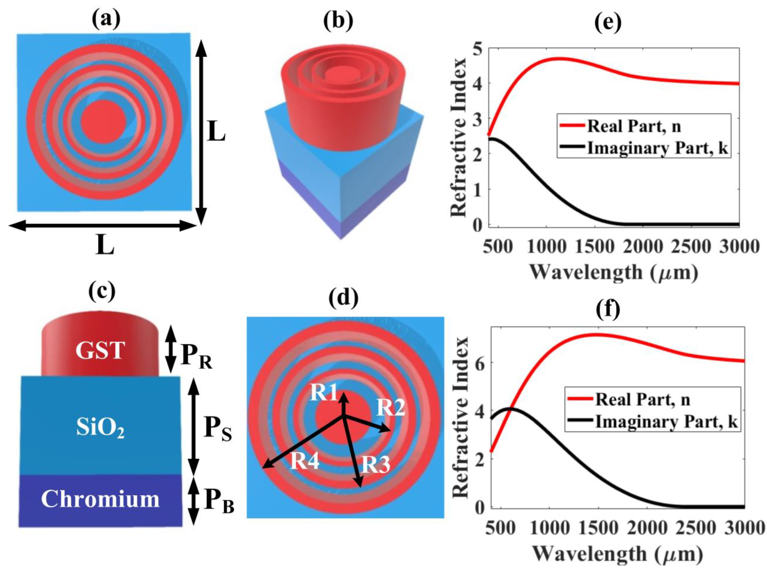
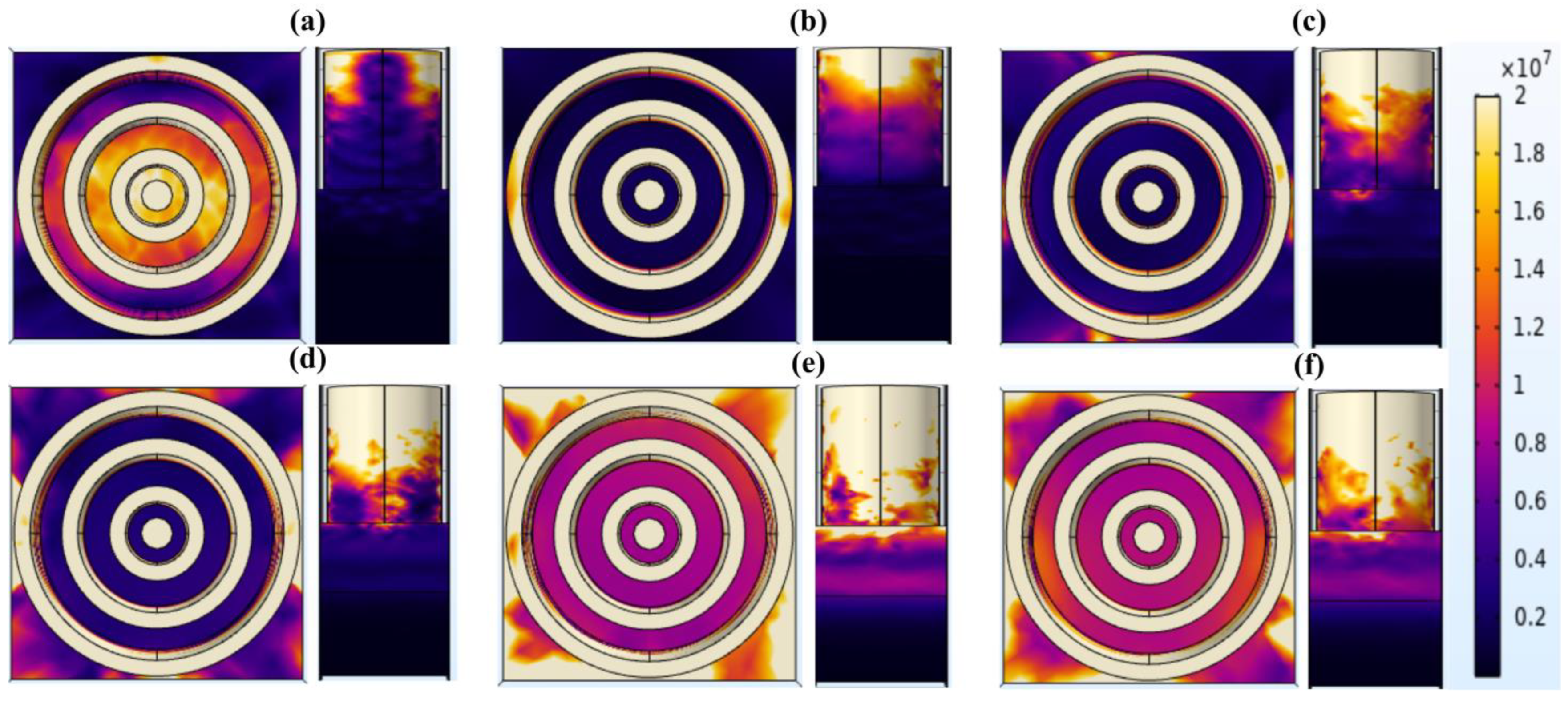
2.1. Design and Modeling

The design and modeling process of the proposed broadband solar absorber is described through a flowchart in Figure 1. Figure 2a shows the top view for the GST ring resonator. Figure 2b represents the 3D shape of the concentric GST ring resonator-based solar absorber. Figure 2c represents the front view for the GST ring resonator with the respective parameters such as the structure length L = 500 nm; the ground layer thickness, PB is 500 nm; the substrate layer thickness, PS is 600 nm; and the GST ring resonator thickness, PR is also 500 nm. Figure 2d shows the radius of the rings, respectively. The radius of the central circle R1 is 25 nm. The first ring radius R2 is 50 nm, the second ring radius R3 is 125 nm, and the third ring radius R4 is 200 nm. To investigate the concentric ring resonator design, we used COMSOL Multiphysics software [38]. The refractive index of Cr is 3.212 and the silicon dioxide SiO2 refractive index is 1.5175 [39]. The proposed design is developed with a SiO2 substrate layer over the Cr ground layer and a GST ring resonator is placed over the SiO2 layer. Figure 2e,f represent the refractive index output for aGST and cGST with real and imaginary parts, respectively. A SiO2 material as a substrate is chosen due to its dielectric properties [40,41]. Due to its remarkable optical properties and high melting point, chromium metal is selected as the ground layer [39].

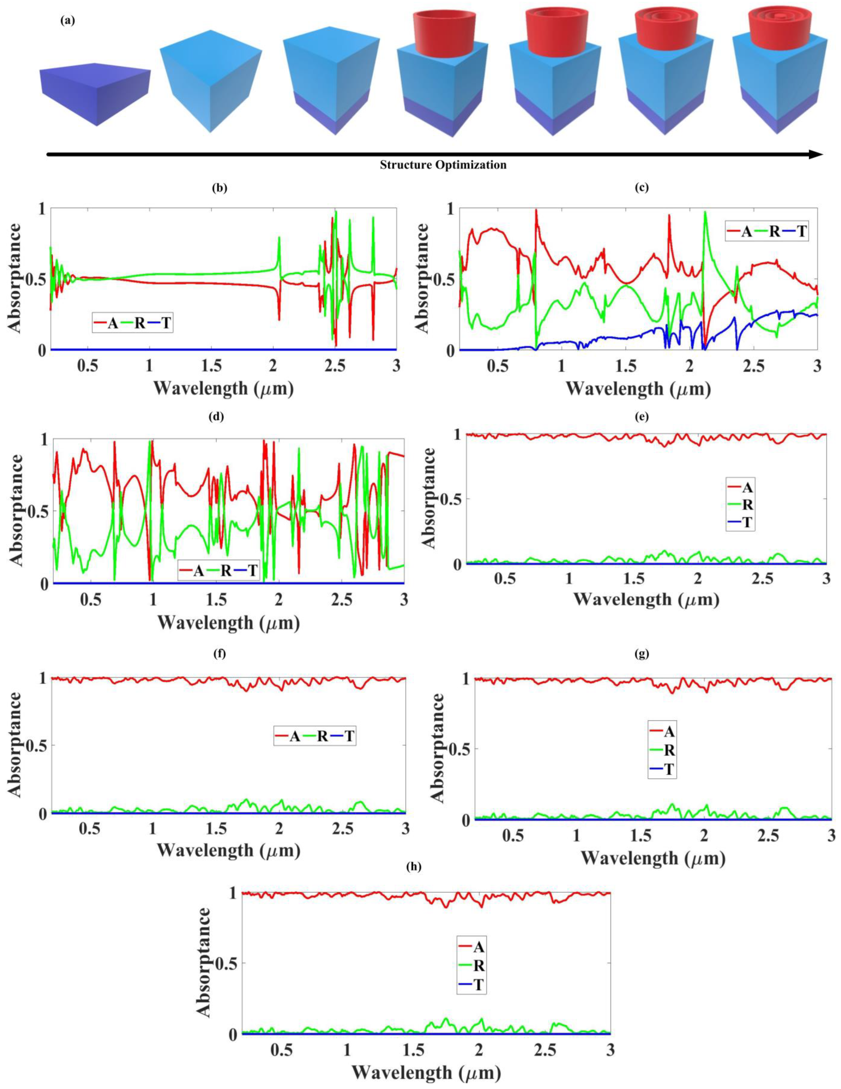
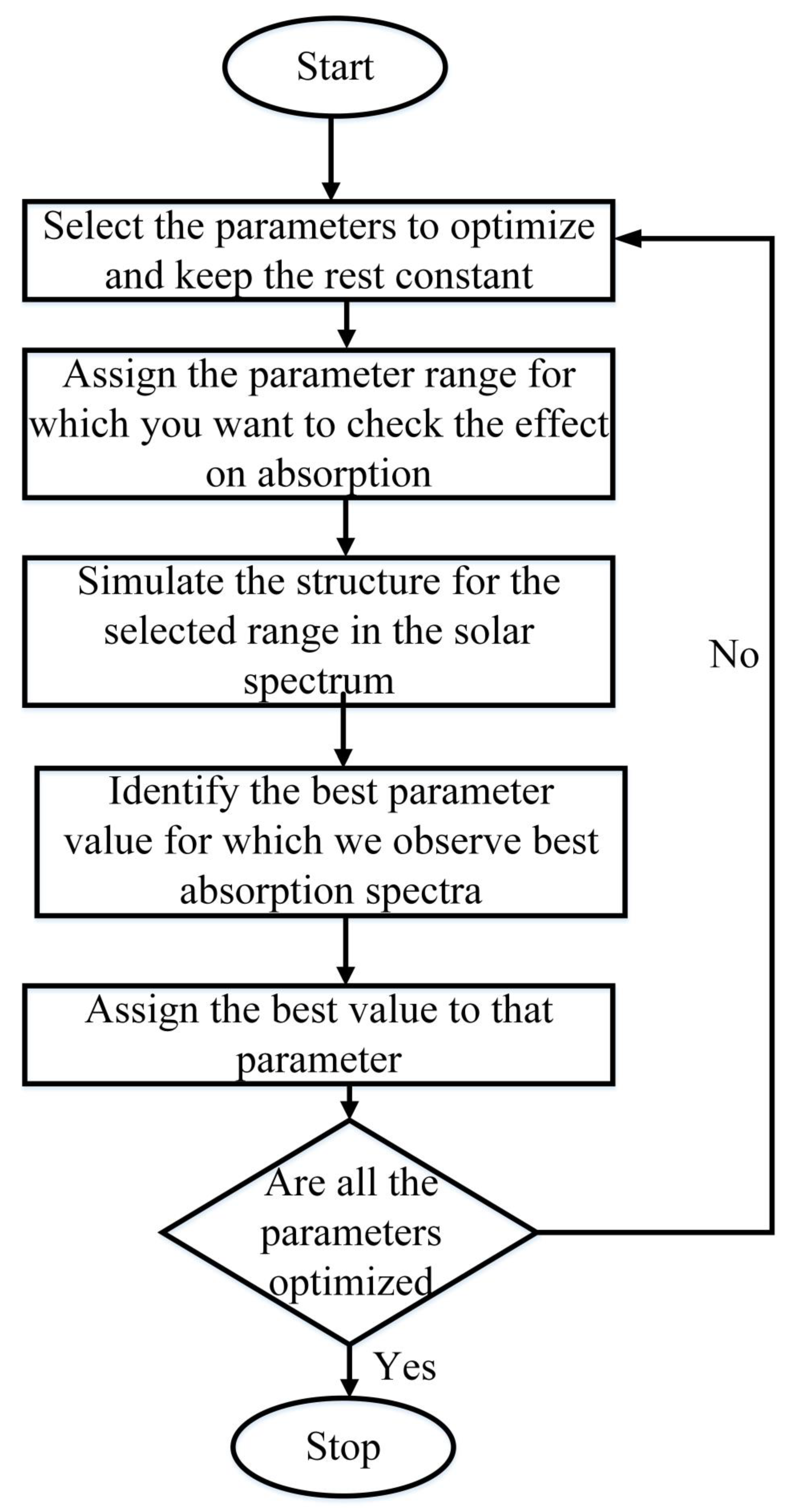
2.2. Structure Optimization

The main importance and novelty of the proposed concentric ring resonator is its symmetrical shape, which in return gives the polarization insensitive response which is a necessity for a solar absorber. Furthermore, the material used to fabricate ring resonators is less compared to circular resonators, and it is also easy to fabricate with the help of photolithography. Figure 3a presents the process of optimizing a developed structure by simulating and checking the importance of each layer and how they contribute towards improving the absorption response step by step. First, we built a Cr ground layer. On the Cr ground layer, we placed a SiO2 layer, and we constructed the ring resonator over the SiO2 layer. Then, the second ring resonator, third ring resonator, and finally the one cylinder were constructed concentrically. Figure 3b–h represents the situations of absorptance, reflectance, and transmittance of the developed designs of Figure 3a. The average absorption rates of the various structures were calculated by the FEM method [42].
In Figure 3b, the average absorption rate of the Cr ground layer in UV, V, NIR, and MIR regions is presented. The absorption rates are 48.28%, 50.45%, 46.41%, and 45.76% in the mentioned ranges, respectively, with an overall absorption rate of 46.96%. Figure 3c examines the average absorption rate of the SiO2 substrate layer in UV, V, NIR, and MIR regions, and the absorption rates are 70.77%, 77.53%, 54.79%, and 53.83%, respectively, with the overall absorption rate of 58.16%. The absorption rate of the design comprised both the Cr ground layer and SiO2 substrate layer and is shown in Figure 3d. In this figure, the absorption rates are 68.24%, 78.66%, 60.77%, and 62.27% in UV, V, NIR, and MIR regions, respectively, and the overall average absorption rate is 63.48%. Then, we continued to develop the GST ring resonator with the first ring, and the absorption rate is shown in Figure 3e. In this figure, the average absorption rate is significantly higher than the previous structures with 98.52%, 98.47%, 96.92%, and 97.44% in UV, V, NIR, and NIR, respectively. The overall average absorption rate is also increased to 97.3%. The second ring resonator is then included, and the absorption rates are 98.49%, 98.43%, 96.18%, and 97.38% in UV, V, NIR, and MIR, respectively, and the overall absorption rate mentioned is 97.32%, as shown in Figure 3f. The absorption results of the third ring structure are presented in Figure 3g including 98.47%, 98.44%, 97.97%, and 97.58% in UV, V, NIR, and MIR regions, respectively, and the average overall rate is 97.35%. In Figure 3h, the overall design is developed, and the absorption results are 98.52%, 98.45%, 97.15%, and 97.45% in UV, V, NIR, and MIR regions, respectively. The overall average absorption rate is 97.36%, so the average absorption rate gets higher when we develop the new layers in the proposed design. One interesting trend that we observed is when we removed the ground plane, the transmittance started to increase, as we can observe in Figure 3c; this is since the ground layer transmits back the electromagnetic (EM) waves and in absence of this, the EM waves are reflected. The flowchart presented in Figure 4 describes the process of optimizing the structural parameters used for the proposed study.

3. Results and Discussion

In this part, the effect of various structural parameters and the phases of GST are investigated, with the corresponding results discussed in detail. Figure 5a shows the absorptance (A), reflectance (R), and transmittance (T) of the aGST concentric ring resonator solar absorber. For the wavelength range between 0.2 and 1.59 µm, the absorption rate is above 97% with a bandwidth of 1390 nm; the average absorption is 98.18% for this particular bandwidth. The absorption rate is also above 97% in the wavelength between 1.84 and 3 µm with a bandwidth of 1160 nm and a mean absorption of 97.14%. The overall wavelength ranges between 0.2 and 3 µm from UV to MIR and shows an absorption rate above 95% with a bandwidth of 2800 nm. We can assign six peak wavelengths (in micrometers) to show the unity absorption rate of the aGST ring resonator solar absorbers such as λ1 = 0.25, λ2 = 0.61, λ3 = 1.24, λ4 = 1.84, λ5 = 2.53, and λ6 = 2.91. Figure 5b presents the average absorptance, reflectance, and transmittance for the cGST concentric ring resonator solar absorber with the same parameters as aGST. We can see the decreased absorption rate and increased reflectance rate in the cGST compared to the aGST results. Therefore, the absorption rate in the ring resonator solar absorber using aGST is better than cGST.
Figure 5c shows the comparison data flow chart of the average absorption rate of aGST and cGST in UV, V, NIR, MIR, and overall ranges. In the data plot, the absorption rate of aGST is represented by the color green and cGST is represented by the color yellow. The average absorption rate in aGST is decreased compared to the cGST in the UV region; however, the average absorption rate in aGST is increased compared to the cGST consisting of V, NIR, MIR, and overall regions. In the UV region, the absorption rate of aGST is 96.33% and cGST is 96.99%, which is a very slight difference. In V, NIR, and MIR regions, the absorption rate of aGST is 94.48%, 94.51%, and 97.71%, respectively; on the other hand, the decreased absorption rate of cGST is 93.59%, 91.55%, and 95.95%, respectively. Therefore, we can observe that the overall average absorption rate in cGST is slightly decreased compared to the aGST in the data plot.
The proposed aGST concentric ring resonator solar absorber can be examined by the AM1.5 radiation systems mentioned in Figure 5d. In this figure, the AM1.5 section is in red, the absorption section under the solar radiation region is in yellow, and the regions of missed solar energy are in blue. By using Equation (1), we can obtain the numerical values of the absorption section and missed solar energy [43]. To develop the good efficiency and higher absorption rate of the proposed aGST concentric ring resonator solar absorber, we need to improve the absorbed solar energy under the solar radiation region and reduce the missed solar energy nearly to zero for all the ranges from ultraviolet to MIR regions [44]. To calculate the amount of solar energy radiated from the sun, we need to use the following AM1.5 equation [45].
η A = λ m i n λ m a x 1 R ω . I A M 1.5 ω . d ω λ m i n λ m a x I A M 1.5 ω . d ω
From the above equation, the ultra-broadband absorption rate under normal solar radiation conditions is assigned by A, IAM for an air mass 1.5 irradiances, and the reflectance of solar energy is denoted by R [46].
The difference between the conventional and proposed optimization technique is as follows:
There are two main methods for optimization used by researchers based on their behavior [47].
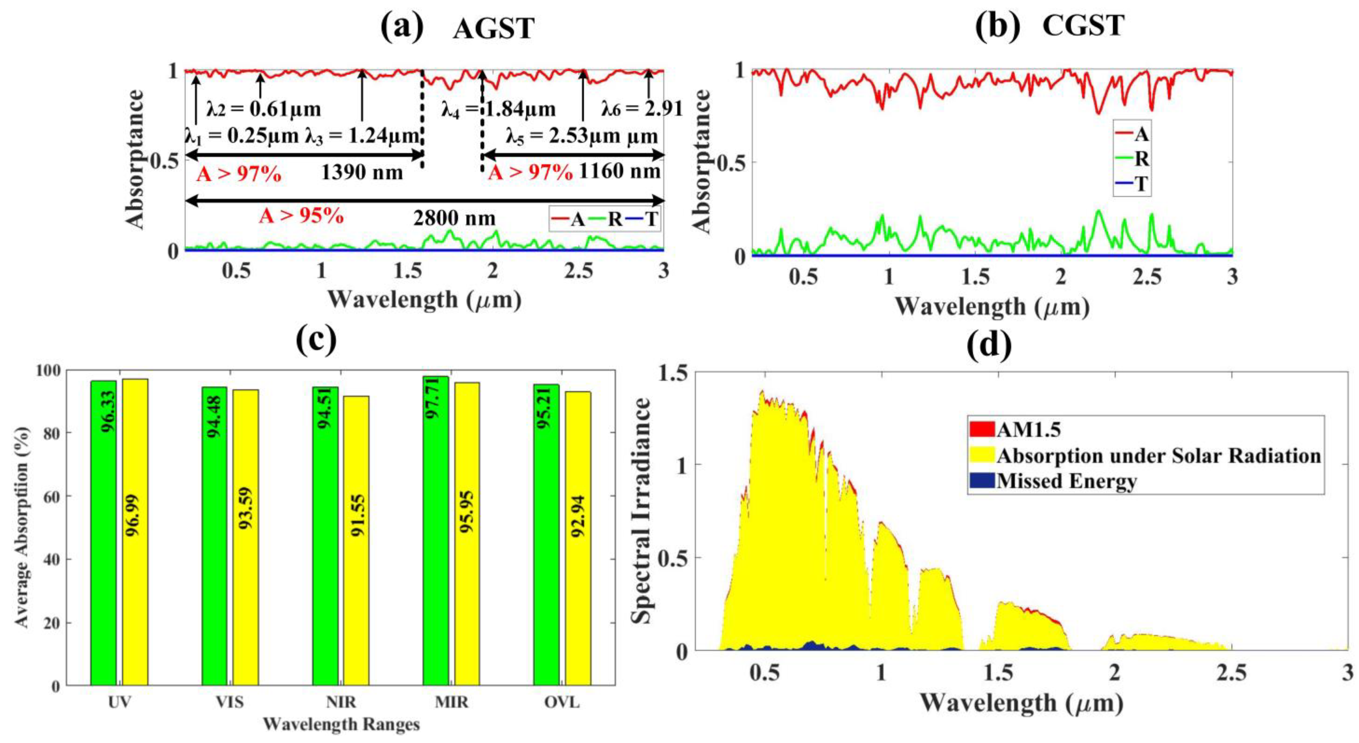
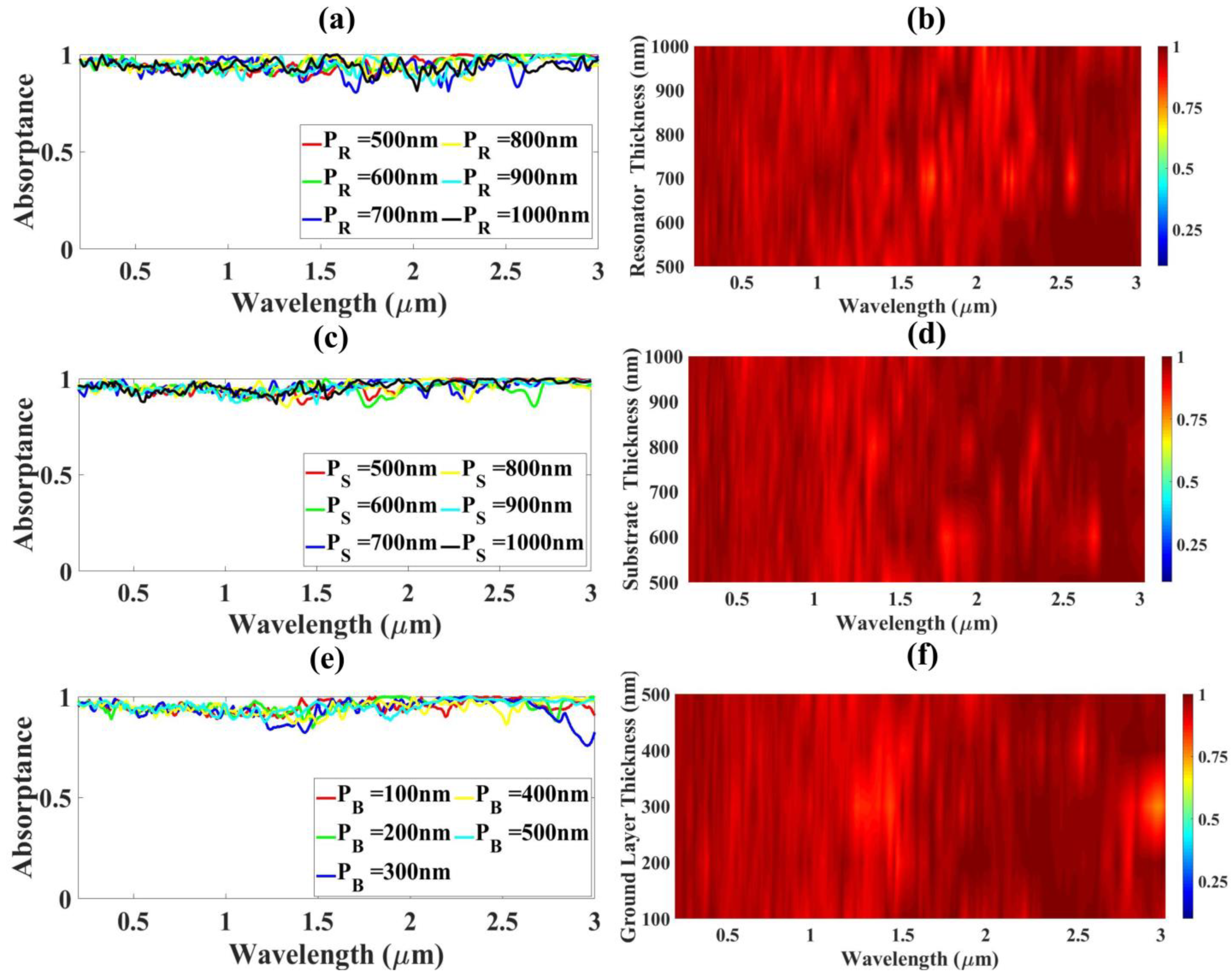
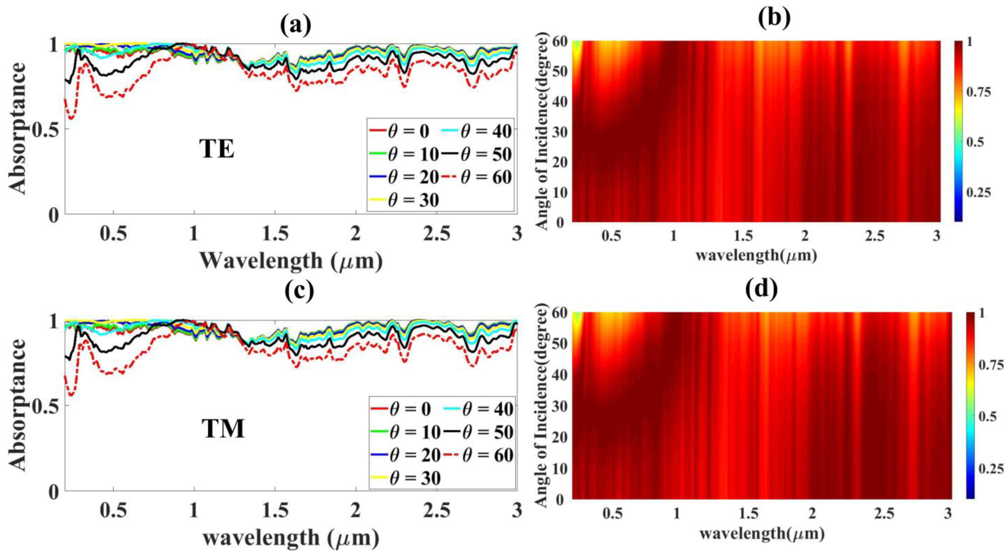
  • Linear Parametric Optimization
  • Nonlinear Parametric Optimization
As our response has behaved nonlinearly with wavelength, we have used the nonlinear parametric optimization technique for optimizing our structural parameters, such as GST concentric ring resonator thickness, substrate thickness, and Cr ground layer thickness.
We can analyze the absorption rate of the developed ultra-broadband GST ring resonator design by changing the numerous parameters of the GST resonator thickness, SiO2 substrate layer, and Cr ground layer as shown in Figure 6. The output of the absorption rate changes by increasing the GST resonator thickness from 500 nm to 1000 nm, shown in Figure 6a,b with the help of line plots as well as the fermi plot. At the first peak wavelength λ1, the average absorption rate increases from 96.48% to 97.79% by changing the aGST resonator thickness from 500 nm to 1000 nm. For the next three peak wavelengths λ2, λ3, and λ4, the absorption rate also increases from 91.01%, 88.88%, and 93.61% to 96.93%, 97.62%, and 97.47% when the aGST resonator thickness changes to between 500 nm and 1000 nm, respectively. The absorption rate of the last two peak wavelengths λ5 and λ6 decreases from 99.58% and 99.92% to 98.54% and 98.85%, respectively. So, the overall ranges of aGST resonator thickness from 500 nm to 1000 nm decreases from 95.47% to 94.05%, and also slightly decreases in the ultraviolet, violet, NIR, and MIR regions. The fermi plot of the absorption rate changes by the GST resonator thickness from 500 to 1000 nm is shown in Figure 6b.
The output of the absorption rates by the substrate thickness changes between 500 nm and 1000 nm at the six peak wavelength ranges between 0.2 and 3 µm is shown in Figure 6c,d, shown by the fermi plot. The increased average absorption rate of the substrate thickness from 500 nm to 1000 nm at the first four wavelengths λ1, λ2, λ3, and λ4 is 96.67%, 92.78%, 91.28%, and 98.32% from 96.48%, 91.01%, 88.88%, and 93.61%, respectively. The absorption rate of the substrate thickness decreased from 99.58% and 99.92% to 96.43% and 99.63% at the λ5 and λ6, respectively. When we increased the substrate thickness from 500 nm to 1000 nm, the overall absorption rate showed just a little change from 95.47% to 95.92%; this was also the same situation in the UV, V, NIR, and MIR regions.
When we increased the ground layer thickness between 500 nm and 900 nm at the six peak wavelength ranges between 0.2 and 3 µm, the output of the absorption rate changes is shown in Figure 6e, and the fermi plot is shown in Figure 6f. At the first peak wavelength λ1, the absorption rate is increased from 95.96% to 96.74% when the ground layer thickness changes between 100 nm and 500 nm. On the other hand, the absorption rates decreased from 94.88%, 91.04%, 93.27%, 98.46, and 97.14% to the absorption rates 92.55%, 90.36%, 91.68%, 96.35%, and 96.37%, respectively, when we changed the ground layer thickness from 100 nm to 500 nm at another five peak wavelengths λ2, λ3, λ4, λ5, and λ6. The overall absorption rate is equal to the absorption rate of 95.2%, and the absorption rates at the UV, V, NIR, and MIR regions are also equal at the increased ground layer thickness between 100 nm and 500 nm with the six peak wavelengths ranging between 0.2 and 3 µm. The fermi plot of the absorption rate changes when we increased the ground layer thickness from 100 nm to 500 nm is presented in Figure 6f.
To develop the ultra-broadband GST ring solar absorber with a good average absorption rate, we need to analyze some sections such as GST resonator, SiO2 substrate layer thickness, Cr ground layer thickness, and incidence angles in (TE) and (TM) modes by changing the structural parameters numerically [48]. The absorption rate of the concentric GST ring solar absorber in the TE mode with the angle of incidence changes from 0 to 60 degrees at the wavelength range from 0.2 to 3 µm is presented in Figure 7a and by the fermi plot in Figure 7b. The five peak wavelengths λ1, λ2, λ4, λ5, and λ6 (all except λ3) show decreased absorption rates from 95.96%, 93.24%, 89.97%, 96.99%, and 97.62% to 67.49%, 73.52%, 91.79%, 87.41%, and 84.71%, respectively.
Only one wavelength λ3 shows an increased absorption rate from 89.97% to 91.79%. The absorption rate of the concentric GST ring solar absorber in TE mode by the fermi plot is presented in Figure 7b. The average absorption rate of the concentric GST ring solar absorber in TM mode with the angle of incidence changes from 0 to 60 degrees at the wavelength range from 0.2 to 3 µm is shown in Figure 7c and by the fermi plot in Figure 7d. The results of the absorption rates in the TE mode also changed, as in the TM mode. In the TM mode, the output of five peak wavelengths λ1, λ2, λ4, λ5, and λ6 (all except λ3) show decreased absorption rates from 95.96%, 93.24%, 96.15%, 98.32%, and 98.53% to 67.49%, 73.52%, 82.77%, 89.43%, and 83.42%, respectively. Only one wavelength, also λ3, shows an increased absorption rate from 90.01% to 91.83%. The absorption rate of the concentric GST ring solar absorber in TM mode by the fermi plot is exhibited in Figure 7d. From the comparison of the TE and TM modes, we can see the overall absorption rates do not have many changes in percentages. For the TE mode, the overall absorption rate significantly decreased from 94.45% to 83.19%. For the TM mode, the overall absorption rate significantly also decreased from 94.78% to 83.31%. In the ultraviolet region for both TE and TM modes, the absorption rate decreased from 96.04% to 73.27%. In the TE mode, the absorption rate of V, NIR, and MIR decreased from 94.9%, 93.71%, and 96.28% to 85.8%, 83.89%, and 83.9%, respectively. Comparing the TE mode to the TM mode, the absorption rates in V, NIR, and MIR also decreased from 94.9%, 94.03%, and 96.99% to 86.08%, 83.59%, and 83.6%, respectively. Therefore, in both the TE mode and TM mode, the absorption rate is above 95% in the UV and MIR regions and above 90% in the V and NIR regions by changing the angle of incidences (degrees) from 0 to 60 with the wavelength range of 0.2–3 µm. In Table 1, we can express the absorption rate in percentages with the respective bandwidth by changing the angle insensitive in the UV, V, NIR, and MIR regions with a wavelength range of 0.2 to 3 µm. The proposed structure demonstrates an almost identical response for 0 to 60 degrees, after which the response gets affected and the absorption decreases after 60 degrees. This limitation can be avoided by creating a platform to place a solar absorber structure to avoid solar energy coming from more than 60 degrees of the incidence angle.
The situations of electric field intensity changes in the concentric ring aGST resonator for the six peak wavelengths in micrometers (µm) such as λ1 = 0.25, λ2 = 0.61, λ3 = 1.24, λ4 = 1.84, λ5 = 2.53, and λ6 = 2.91 are exhibited in Figure 8a–f, respectively. The amount of the electric field intensity is also important for developing the absorption rate of the GST ring resonators in UV, V, NIR, and MIR. The electric field intensity changes in the x-y and x-z planes are mentioned in Figure 8a,b. At the first peak wavelength λ1 = 0.25 µm, the amount of the electric field intensity is better at the inner part of the ring resonator and at the top of the absorber layer, as shown in Figure 8a in both the x-y and x-z planes, and the absorption rate is 96.74%. At the second peak wavelength λ2 = 0.61 µm, the amount of electric field intensity is better at the resonator rings compared to the other parts of the proposed broadband design, and the top absorber layer is presented in Figure 8b in both the x-y and x-z planes, and the absorption rate is 92.55%. At the wavelengths of λ3 = 1.24 µm and λ4 = 1.84 µm, the decreased amount of the electric field intensity to the other wavelengths of the proposed design is presented in Figure 8c,d in both the x-y and x-z planes, and the absorption rate is 90.36% and 91.68%, respectively. In Figure 8e,f, the amount of electric field intensity is significantly increased at the ring resonators and gives the higher absorption rate of 96.35% and 96.37% at the wavelengths of λ5 = 2.53 µm and λ6 = 2.91 µm in the UV, V, NIR, and MIR ranges, respectively. In Table 1, we have compared the proposed design’s absorption rate to the other published papers, and it can be found that the developed GST ring resonator design can provide better results than the other published paper’s results. Therefore, the proposed concentric GST ring resonator design can be used to develop many photonic devices with a higher absorption rate. The absorption characteristics depend on the electromagnetic field, as discussed in Figure 5 above. To better understand the best factors affecting absorption, we analyzed the significance of the angles of incidence (IAS) for both the TE and TM modes.

4. Conclusions

A MIM solar energy absorber has been simulated, designed, and theoretically proven and is achieving an optimal average absorption response of 96.52% in the visible region and a maximum absorptivity of 99.98%. Chromium metal is utilized as the ground layer because of its transmittance blocking properties; the substrate layer of SiO2 dielectric insulator is used since it provides lossless resonance characteristics, and the concentric ring resonator is made of GST, as it has good impedance matching characteristics. The proposed aGST ring resonator solar absorber represents a good absorption rate over the wavelength range from 0.2 to 3 µm. For the bandwidth range of 2550 nm, the solar absorption rate is located above 97% between the wavelength range 0.2 and 1.59 µm and 1.84 to 3 µm, and the average absorption rate is 98.18%, and 97.14%, respectively. The overall wavelength between 0.2 and 3 µm from UV to MIR regions shows an absorption rate above 95% with a bandwidth of 2800 nm. A broadband absorption response is achieved, which is the combination of multiple near-perfect absorption peaks that can be validated by the electric field distribution plots. We have developed a good quality structural design with a higher absorption rate with wide angle and polarization insensitiveness, a lower reflectance rate, and zero transmittance. This design can be applied for improving the performance of thermoelectric photovoltaic systems.

Author Contributions

Conceptualization, S.K.P. and K.A.; methodology, B.B.H. and J.S.; software, B.B.H., J.S. and K.A.; validation, B.B.H., M.A. and A.A.; formal analysis, K.A., M.A., A.A. and J.S.; investigation, K.A., S.K.P., J.S. and A.A.; resources, A.A. and B.B.H.; writing—original draft preparation, All Authors; writing—review and editing, K.A., S.K.P. and J.S.; visualization, B.B.H. and J.S.; supervision, S.K.P. and K.A. All authors have read and agreed to the published version of the manuscript.

Funding

This research received no external funding.

Institutional Review Board Statement

Not applicable.

Informed Consent Statement

Not applicable.

Data Availability Statement

The data will be made available at a reasonable request to corresponding author.

Conflicts of Interest

The authors declare no conflict of interest.

References

  1. Lønborg, C.; Carreira, C.; Jickells, T.; Álvarez-Salgado, X.A. Impacts of Global Change on Ocean Dissolved Organic Carbon (DOC) Cycling. Front. Mar. Sci. 2020, 7, 466. [Google Scholar] [CrossRef]
  2. Gamon, J.A.; Huemmrich, K.F.; Wong, C.Y.S.; Ensminger, I.; Garrity, S.; Hollinger, D.Y.; Noormets, A.; Peñuelask, J. A remotely sensed pigment index reveals photosynthetic phenology in evergreen conifers. Proc. Natl. Acad. Sci. USA 2016, 113, 13087–13092. [Google Scholar] [CrossRef] [PubMed] [Green Version]
  3. Park, Y.; Kim, J.; Roh, Y.G.; Park, Q.H. Optical slot antennas and their applications to photonic devices. Nanophotonics 2018, 7, 1617–1636. [Google Scholar] [CrossRef]
  4. Fang, T.; Gao, X.; Wang, X.; Liu, J. Design of gate-tunable graphene electro-optical reflectors based on an optical slot-antenna coupled cavity. J. Phys. Photonics 2021, 3, 045003. [Google Scholar] [CrossRef]
  5. Zhou, J.; Leaño, J.L.; Liu, Z.; Jin, D.; Wong, K.L.; Liu, R.S.; Bünzli, J.C.G. Impact of Lanthanide Nanomaterials on Photonic Devices and Smart Applications. Small 2018, 14, 1801882. [Google Scholar] [CrossRef]
  6. Liu, Z.; Zhang, H.; Fu, G.; Liu, G.; Liu, X.; Yuan, W.; Xie, Z.; Tang, C. Colloid templated semiconductor meta-surface for ultra-broadband solar energy absorber. Sol. Energy 2020, 198, 194–201. [Google Scholar] [CrossRef]
  7. Krumme, J.-P.; Hack, R.A.A.; Raaijmakers, I.J.M.M.; Cazzaniga, A.; Crovetto, A.; Ettlinger, R.B.; Canulescu, S.; Hansen, O.; Pryds, N.; Schou, J.J.; et al. Photovoltaic Energy Conversion, 2003. Proceedings of 3rd World Conference on. Thin Solid Films 2011, 3, 1–4. [Google Scholar]
  8. Jalal, R.; Shihab, S.; Alhadi, M.A.; Rasheed, M. Spectral Numerical Algorithm for Solving Optimal Control Using Boubaker-Turki Operational Matrices. J. Phys. Conf. Ser. 2020, 1660, 012090. [Google Scholar] [CrossRef]
  9. Rasheed, M.; Mohammed, O.Y.; Shihab, S.; Al-Adili, A. A comparative Analysis of PV Cell Mathematical Model. J. Phys. Conf. Ser. 2021, 1795, 012042. [Google Scholar] [CrossRef]
  10. Ding, F.; Cui, Y.; Ge, X.; Jin, Y.; He, S. Ultra-broadband microwave metamaterial absorber. Appl. Phys. Lett. 2012, 100, 103506. [Google Scholar] [CrossRef] [Green Version]
  11. Nuru, Z.Y.; Arendse, C.J.; Muller, T.F.; Khamlich, S.; Maaza, M. Thermal stability of electron beam evaporated AlxO y/Pt/AlxOy multilayer solar absorber coatings. Sol. Energy Mater. Sol. Cells 2014, 120, 473–480. [Google Scholar] [CrossRef]
  12. Zaversky, F.; Aldaz, L.; Sánchez, M.; Ávila-Marín, A.L.; Roldán, M.I.; Fernández-Reche, J.; Füssel, A.; Beckert, W.; Adler, J. Numerical and experimental evaluation and optimization of ceramic foam as solar absorber—Single-layer vs multi-layer configurations. Appl. Energy 2018, 210, 351–375. [Google Scholar] [CrossRef]
  13. Patel, S.K.; Udayakumar, A.K.; Mahendran, G.; Vasudevan, B.; Surve, J.; Parmar, J. Highly efficient, perfect, large angular and ultrawideband solar energy absorber for UV to MIR range. Sci. Rep. 2022, 12, 18044. [Google Scholar] [CrossRef] [PubMed]
  14. Patel, S.K.; Surve, J.; Katkar, V.; Parmar, J. Optimization of Metamaterial-Based Solar Energy Absorber for Enhancing Solar Thermal Energy Conversion Using Artificial Intelligence. Adv. Theory Simul. 2022, 5, 2200139. [Google Scholar] [CrossRef]
  15. Patel, S.K.; Surve, J.; Prajapati, P.; Taya, S.A. Design of an ultra-wideband solar energy absorber with wide-angle and polarization independent characteristics. Opt. Mater. 2022, 131, 112683. [Google Scholar] [CrossRef]
  16. Patel, S.K.; Surve, J.; Parmar, J.; Katkar, V.; Jadeja, R.; Taya, S.A.; Ahmed, K. Graphene-based metasurface solar absorber design for the visible and near-infrared region with behavior prediction using Polynomial Regression. Optik 2022, 262, 169298. [Google Scholar] [CrossRef]
  17. Thomas, N.H.; Chen, Z.; Fan, S.; Minnich, A.J. Semiconductor-based Multilayer Selective Solar Absorber for Unconcentrated Solar Thermal Energy Conversion. Sci. Rep. 2017, 7, 5362. [Google Scholar] [CrossRef] [Green Version]
  18. Patel, S.K.; Surve, J.; Jadeja, R.; Katkar, V.; Parmar, J.; Ahmed, K. Ultra-Wideband, Polarization-Independent, Wide-Angle Multilayer Swastika-Shaped Metamaterial Solar Energy Absorber with Absorption Prediction using Machine Learning. Adv. Theory Simul. 2022, 5, 2100604. [Google Scholar] [CrossRef]
  19. AL-Rjoub, A.; Rebouta, L.; Costa, P.; Vieira, L.G. Multi-layer solar selective absorber coatings based on W/WSiAlNx /WSiAlOyNx/SiAlOx for high temperature applications. Sol. Energy Mater. Sol. Cells 2018, 186, 300–308. [Google Scholar] [CrossRef]
  20. Xin, W.; Binzhen, Z.; Wanjun, W.; Junlin, W.; Junping, D. Design and characterization of an ultrabroadband metamaterial microwave absorber. IEEE Photonics J. 2017, 9, 1–13. [Google Scholar] [CrossRef]
  21. Du John, H.V.; Jose, T.; Jone, A.A.A.; Sagayam, K.M.; Pandey, B.K.; Pandey, D. Polarization Insensitive Circular Ring Resonator Based Perfect Metamaterial Absorber Design and Simulation on a Silicon Substrate. Silicon 2022, 14, 9009–9020. [Google Scholar] [CrossRef]
  22. Niranjan, K.; Kondaiah, P.; Biswas, A.; Kumar, V.P.; Srinivas, G.; Barshilia, H.C. Spectrally selective solar absorber coating of w/walsin/sion/sio2 with enhanced absorption through gradation of optical constants: Validation by simulation. Coatings 2021, 11, 334. [Google Scholar] [CrossRef]
  23. Wu, B.; Liu, Z.; Du, G.; Shi, L.; Liu, X.; Liu, M.; Zhan, X. Ultra-broadband electromagnetic wave absorber based on split-ring resonators. J. Opt. Soc. Am. B 2019, 36, 3573. [Google Scholar] [CrossRef]
  24. IEEE MTT-S International Microwave and RF Conference 2014, IMaRC 2014—Collocated with Intemational Symposium on Microwaves, ISM 2014. 2015, p. 406. Available online: https://www.scimagojr.com/journalsearch.php?q=21100379733&tip=sid&clean=0 (accessed on 12 February 2023).
  25. Yu, P.; Yang, H.; Chen, X.; Yi, Z.; Yao, W.; Chen, J.; Yi, Y.; Wu, P. Ultra-wideband solar absorber based on refractory titanium metal. Renew. Energy 2020, 158, 227–235. [Google Scholar] [CrossRef]
  26. Wu, P.; Wei, K.; Xu, D.; Chen, M.; Zeng, Y.; Jian, R. Ultra-wideband and wide-angle perfect solar energy absorber based on titanium and silicon dioxide colloidal nanoarray structure. Nanomaterials 2021, 11, 2040. [Google Scholar] [CrossRef]
  27. Naveed, M.A.; Bilal, R.M.H.; Baqir, M.A.; Bashir, M.M.; Ali, M.M.; Rahim, A.A. Ultrawideband fractal metamaterial absorber made of nickel operating in the UV to IR spectrum. Opt. Express 2021, 29, 42911–42923. [Google Scholar] [CrossRef]
  28. Shafique, A.; Naveed, M.A.; Ijaz, S.; Zubair, M.; Mehmood, M.Q.; Massoud, Y. Highly efficient Vanadium Nitride based metasurface absorber/emitter for solar-thermophotovoltaic system. Mater. Today Commun. 2023, 34, 105416. [Google Scholar] [CrossRef]
  29. Kondaiah, P.; Niranjan, K.; John, S.; Barshilia, H.C. Tantalum carbide based spectrally selective coatings for solar thermal absorber applications. Sol. Energy Mater. Sol. Cells 2019, 198, 26–34. [Google Scholar] [CrossRef]
  30. Bilal, R.M.H.; Baqir, M.A.; Choudhury, P.K.; Naveed, M.A.; Ali, M.M.; Rahim, A.A. Ultrathin broadband metasurface-based absorber comprised of tungsten nanowires. Results Phys. 2020, 19, 103471. [Google Scholar] [CrossRef]
  31. Zhang, Z.; Yang, J.; He, X.; Zhang, J.; Huang, J.; Chen, D.; Han, Y. Plasmonic refractive index sensor with high figure of merit based on concentric-rings resonator. Sensors 2018, 18, 116. [Google Scholar] [CrossRef] [Green Version]
  32. Liu, P.; Yan, S.; Ren, Y.; Zhang, X.; Li, T.; Wu, X.; Shen, L.; Hua, E. A mim waveguide structure of a high-performance refractive index and temperature sensor based on fano resonance. Appl. Sci. 2021, 11, 10629. [Google Scholar] [CrossRef]
  33. Rio, Y.; Rodríguez-Morgade, M.S.; Torres, T. Modulating the electronic properties of porphyrinoids: A voyage from the violet to the infrared regions of the electromagnetic spectrum. Org. Biomol. Chem. 2008, 6, 1877–1894. [Google Scholar] [CrossRef] [PubMed]
  34. Stauber, T.; Peres, N.M.R.; Geim, A.K. Optical conductivity of graphene in the visible region of the spectrum. Phys. Rev. B Condens. Matter Mater. Phys. 2008, 78, 085432. [Google Scholar] [CrossRef] [Green Version]
  35. Rio, Y.; Rodriguez-Morgade, M.S.; Torres, T. ChemInform Abstract: Modulating the Electronic Properties of Porphyrinoids: A Voyage from the Violet to the Infrared Regions of the Electromagnetic Spectrum. Org. Biomol. Chem. 2008, 39. [Google Scholar] [CrossRef]
  36. Amiri, M.; Tofigh, F.; Shariati, N.; Lipman, J.; Abolhasan, M. Wide-angle metamaterial absorber with highly insensitive absorption for TE and TM modes. Sci. Rep. 2020, 10, 13638. [Google Scholar] [CrossRef] [PubMed]
  37. Volke-Sepulveda, K.; Ley-Koo, E. General construction and connections of vector propagation invariant optical fields: TE and TM modes and polarization states. J. Opt. A Pure Appl. Opt. 2006, 8, 867–877. [Google Scholar] [CrossRef] [Green Version]
  38. COMSOL Multiphysics®, Version 6.0; COMSOL, Inc.: Stockholm, Sweden, 2021.
  39. Rakić, A.D.; Djurišić, A.B.; Elazar, J.M.; Majewski, M.L. Optical properties of metallic films for vertical-cavity optoelectronic devices. Appl. Opt. 1998, 37, 5271. [Google Scholar] [CrossRef] [PubMed]
  40. Ramesh, S.; Kim, H.S.; Lee, Y.J.; Hong, G.W.; Jung, D.; Kim, J.H. Synthesis of cellulose-L-tyrosine-SiO2/ZrO2 hybrid nanocomposites by sol-gel process and its potential. Int. J. Precis. Eng. Manuf. 2017, 18, 1297–1306. [Google Scholar] [CrossRef]
  41. Azad, M.M.; Ejaz, M.; Shah, A.u.R.; Afaq, S.K.; Song, J. A bio-based approach to simultaneously improve flame retardancy, thermal stability and mechanical properties of nano-silica filled jute/thermoplastic starch composite. Mater. Chem. Phys. 2022, 289, 126485. [Google Scholar] [CrossRef]
  42. Zhou, Y.; Li, H.; Li, L.; Cai, Y.; Zeyde, K.; Han, X. Efficient HIE-FDTD method for designing a dual-band anisotropic terahertz absorption structure. Opt. Express 2021, 29, 18611. [Google Scholar] [CrossRef]
  43. Khare, P.; Wadhvani, R.; Shukla, S. Missing Data Imputation for Solar Radiation Using Generative Adversarial Networks. In Proceedings of International Conference on Computational Intelligence: ICCI 2020; Springer: Singapore, 2022; pp. 1–14. [Google Scholar]
  44. Li, Y.; Zhang, L.; Torres-Pardo, A.; González-Calbet, J.M.; Ma, Y.; Oleynikov, P.; Terasaki, O.; Asahina, S.; Shima, M.; Cha, D.; et al. Cobalt phosphate-modified barium-doped tantalum nitride nanorod photoanode with 1.5% solar energy conversion efficiency. Nat. Commun. 2013, 4, 2566. [Google Scholar] [CrossRef] [Green Version]
  45. Zhao, B.; Hu, M.; Ao, X.; Pei, G. Performance analysis of enhanced radiative cooling of solar cells based on a commercial silicon photovoltaic module. Sol. Energy 2018, 176, 248–255. [Google Scholar] [CrossRef]
  46. Rana, A.S.; Zubair, M.; Danner, A.; Mehmood, M.Q. Revisiting tantalum based nanostructures for efficient harvesting of solar radiation in STPV systems. Nano Energy 2021, 80, 105520. [Google Scholar] [CrossRef]
  47. Kler, A.M.; Zharkov, P.V.; Epishkin, N.O. Parametric optimization of supercritical power plants using gradient methods. Energy 2019, 189, 116230. [Google Scholar] [CrossRef]
  48. Radhakrishnan, S.; Kumar, D.S.; Raja, G.T. Design and Simulation Analysis on TM–Pass GST-Assisted Asymmetric Directional Coupler-Based Polarizer. Silicon 2022, 14, 6351–6362. [Google Scholar] [CrossRef]
  49. Liu, Z.; Liu, G.; Huang, Z.; Liu, X.; Fu, G. Ultra-broadband perfect solar absorber by an ultra-thin refractory titanium nitride meta-surface. Sol. Energy Mater. Sol. Cells 2018, 179, 346–352. [Google Scholar] [CrossRef]
  50. Liu, Z.; Liu, G.; Liu, X.; Wang, Y.; Fu, G. Titanium resonators based ultra-broadband perfect light absorber. Opt. Mater. 2018, 83, 118–123. [Google Scholar] [CrossRef]
  51. Gao, H.; Peng, W.; Chu, S.; Cui, W.; Liu, Z.; Yu, L.; Jing, Z. Refractory ultra-broadband perfect absorber from visible to near-infrared. Nanomaterials 2018, 8, 1038. [Google Scholar] [CrossRef] [PubMed] [Green Version]
  52. Soydan, M.C.; Ghobadi, A.; Yildirim, D.U.; Erturk, V.B.; Ozbay, E. All Ceramic-Based Metal-Free Ultra-broadband Perfect Absorber. Plasmonics 2019, 14, 1801–1815. [Google Scholar] [CrossRef] [Green Version]
  53. Tian, X.; Li, Z.-Y. Visible-near infrared ultra-broadband polarization-independent metamaterial perfect absorber involving phase-change materials. Photonics Res. 2016, 4, 146. [Google Scholar] [CrossRef] [Green Version]
  54. Yu, P.; Chen, X.; Yi, Z.; Tang, Y.; Yang, H.; Zhou, Z.; Duan, T.; Cheng, S.; Zhang, J.; Yi, Y. A numerical research of wideband solar absorber based on refractory metal from visible to near infrared. Opt. Mater. 2019, 97, 109400. [Google Scholar] [CrossRef]
Figure 1. Flowchart describing the design process of the proposed broadband solar absorber.
Mathematics 11 01257 g001
Figure 2. Structure of the concentric GST ring resonator-based solar absorber. (a) the top view for the ring resonator, (b) the 3D view for the solar absorber, (c) the front view for the solar absorber with the respective parameters, (d) top view with ring parameters, (e) real (n) and imaginary (k) parts of refractive index for aGST, (f) real (n) and imaginary (k) parts of refractive index for cGST.
Mathematics 11 01257 g002
Figure 3. (a) Construction for the GST ring resonator configuration process step by step, (b) absorptance (A), reflectance (R), and transmittance (T) lines for the Cr ground layer, (c) A, R, and T lines for the SiO2 layer, (d) A, R, and T lines of the construction of both the Cr ground layer and SiO2 layer, (eh) A, R, and T lines by inserting the first GST ring resonator, second GST ring resonator, third GST ring resonator, and the cylinder constructed on the Cr ground layer, and SiO2 layer respectively.
Mathematics 11 01257 g003
Figure 4. Flowchart describing the process of structural parameter optimization.
Mathematics 11 01257 g004
Figure 5. (a) The absorption rate of aGST concentric ring resonator solar absorber between 0.2 and 3 µm, (b) The absorptance, transmittance, and reflectance of cGST, (c) The comparison data plot of absorption rate between aGST in green color and cGST in yellow color for UV, V, NIR, MIR, and overall ranges, (d) aGST absorption under solar radiation missed solar energy concerning AM1.5.
Mathematics 11 01257 g005
Figure 6. The proposed concentric GST ring resonator solar absorber’s absorption rate (a) absorption rate of concentric GST ring resonator solar absorber by increasing the GST ring structural height, PR, (b) absorption rate of concentric GST ring resonator solar absorber by increasing the GST ring structural height, PR demonstrated by fermi plot, (c) absorption rate of concentric GST ring resonator solar absorber by increasing the SiO2 substrate layer thickness, PS, (d) absorption rate of concentric GST ring resonator solar absorber by increasing the SiO2 substrate layer thickness, PS demonstrated by fermi plot, (e) absorption rate of concentric GST ring resonator solar absorber by increasing the Cr ground layer thickness, PB, (f) absorption rate of concentric GST ring resonator solar absorber by increasing the Cr ground layer thickness, PB, demonstrated by the color plot.
Mathematics 11 01257 g006
Figure 7. Concentric GST ring solar absorber’s absorption rates (a) the absorption rate changes of concentric GST ring solar absorber between 0 and 60 degrees in TE mode, (b) the absorption rate changes of concentric GST ring solar absorber between 0 and 60 degrees in TE mode demonstrated by the fermi plot, (c) the absorption rate changes of concentric GST ring solar absorber between 0 and 60 degrees in TM mode, (d) the absorption rate changes of concentric GST ring solar absorber between 0 and 60 degrees in TM mode demonstrated by the fermi plot.
Mathematics 11 01257 g007
Figure 8. The amount of electric field strength in x-y and x-z planes of GST ring resonators at six peak wavelengths in micrometers (µm). (a) λ1 = 0.25, (b) λ2 = 0.61, (c) λ3 = 1.24, (d) λ4 = 1.84, (e) λ5 = 2.53, and (f) λ6 = 2.91.
Mathematics 11 01257 g008
Table 1. Proposed Absorber’s Performance comparison with the available literature.
MIM
Absorber Design
Overall Absorption RateBandwidth (Absorption > 95%)Bandwidth (Absorption > 97%)Angle InsensitivePolarization Insensitive
Ni/SiO2/Ni inspired structure [27]More than 80%-1700 nm0° to 60°Yes
Refractory metal VN based structure [28]-->98% (500 nm)-Yes
W/SiO2/W structure [30]85% (visible)-Near perfect in UV region0° to 60°Yes
TiN & TiO2 disk arrays on SiO2 layer [49]More than 90%1110 (>90%)-0° to 40°Yes
Ti/Silica/Ti double lattice structure [50]91.4%1007 (>90%)-0° to 45°-
Multilayer structure of SiO2/Ti/SiO2/Ti (elliptical nanodisc of Ti) [51]93.26%1650 (>90%)-0° to 70°Yes
All ceramic structure [52]More than 90%1310 (>90%)-0° to 60°Yes
Phase change material based structure [53]More than 90%1000 (>90%)--Yes
TiO2/TiN resonator with SiO2 and TiN as a substrate and ground plane [54]More than 90%1264 (>90%)-0° to 45°-
Proposed concentric GST ring inspired structure95.21%2800 nm2550 nm0° to 60°Yes
Disclaimer/Publisher’s Note: The statements, opinions and data contained in all publications are solely those of the individual author(s) and contributor(s) and not of MDPI and/or the editor(s). MDPI and/or the editor(s) disclaim responsibility for any injury to people or property resulting from any ideas, methods, instructions or products referred to in the content.

