Heterogeneous Integration of GaN and BCD Technologies


Abstract
:1. Introduction
2. Materials and Methods
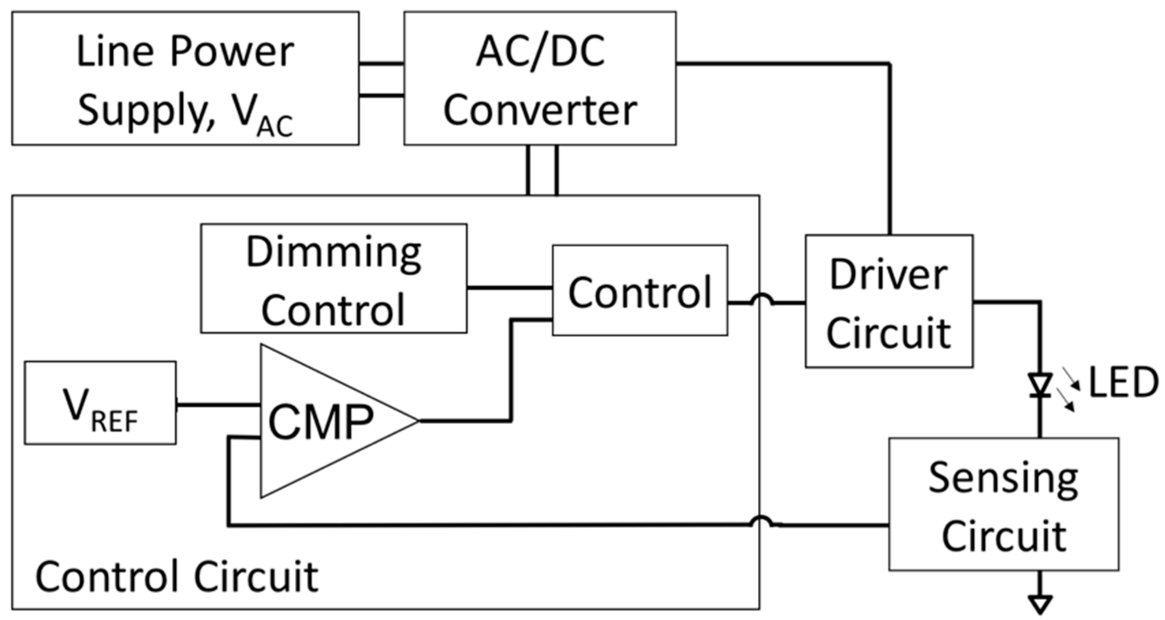
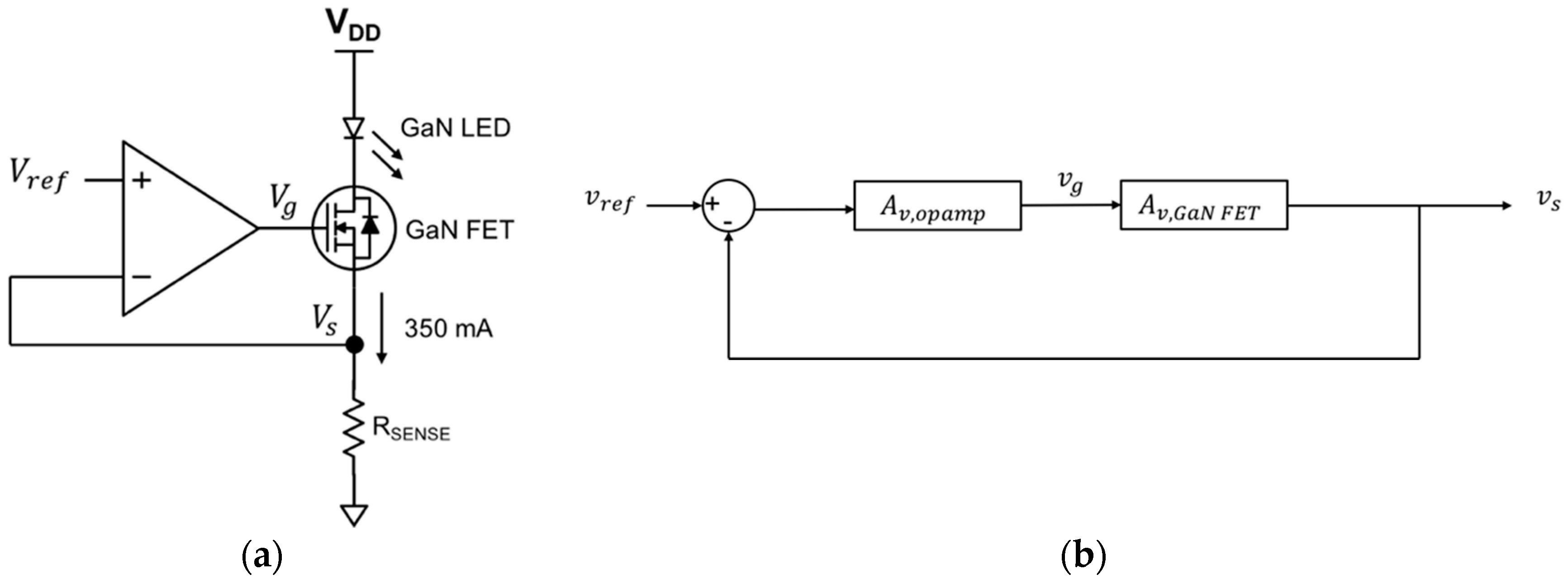
2.1. LED Driver Design
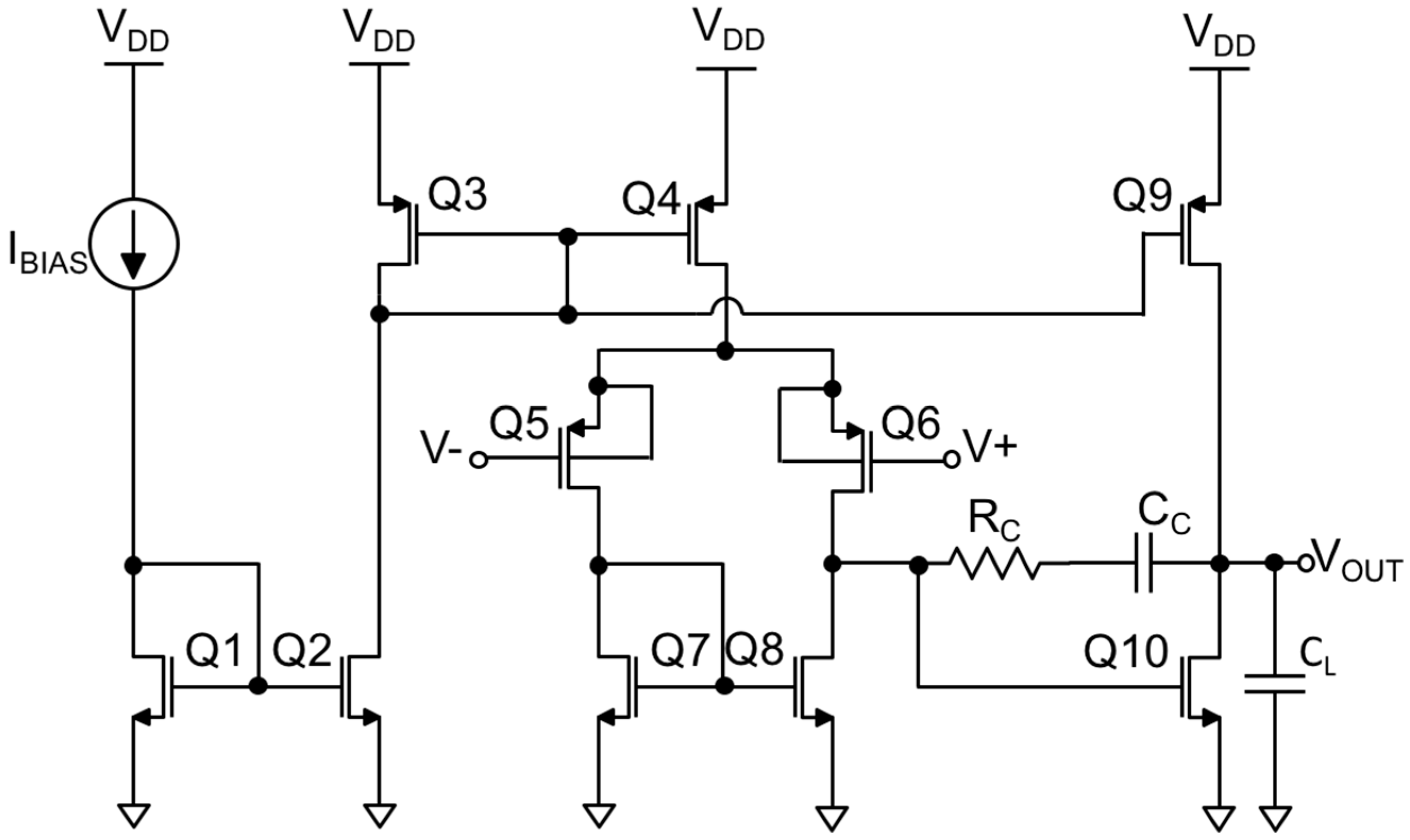
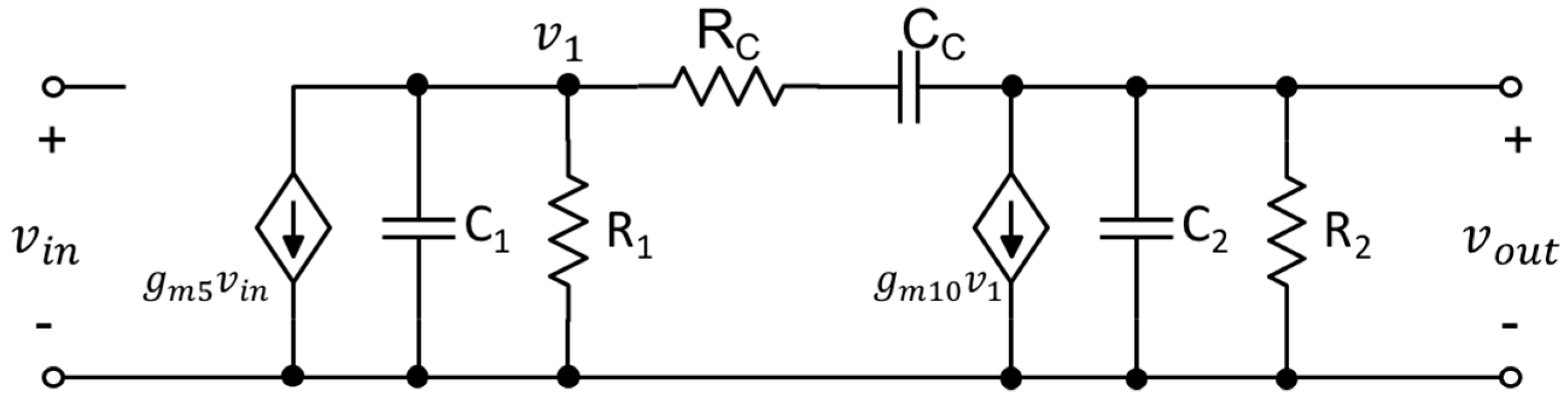
2.1.1. Two-Stage Operational Amplifier (opamp)
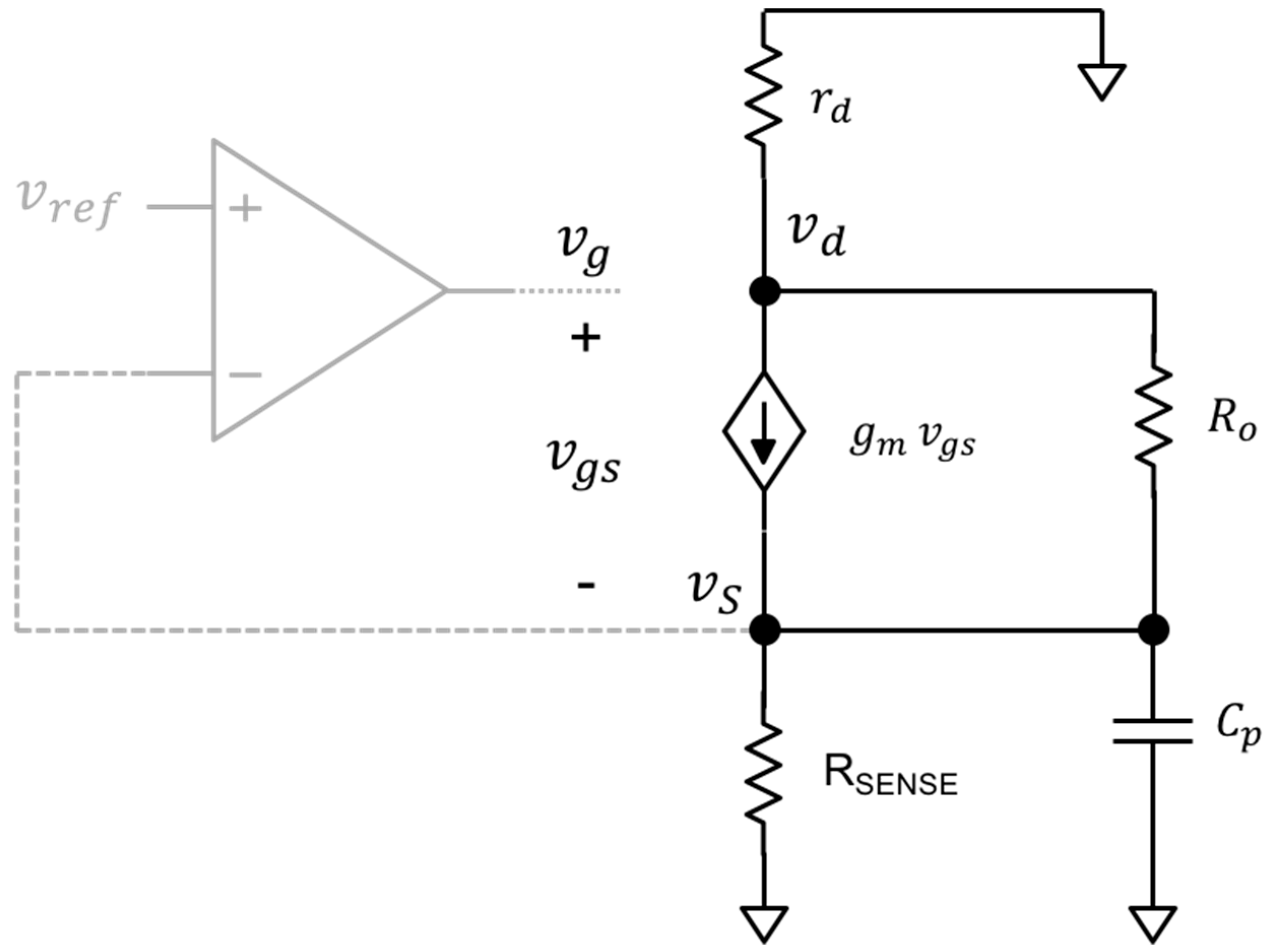
2.1.2. GaN FET Common Drain Stage
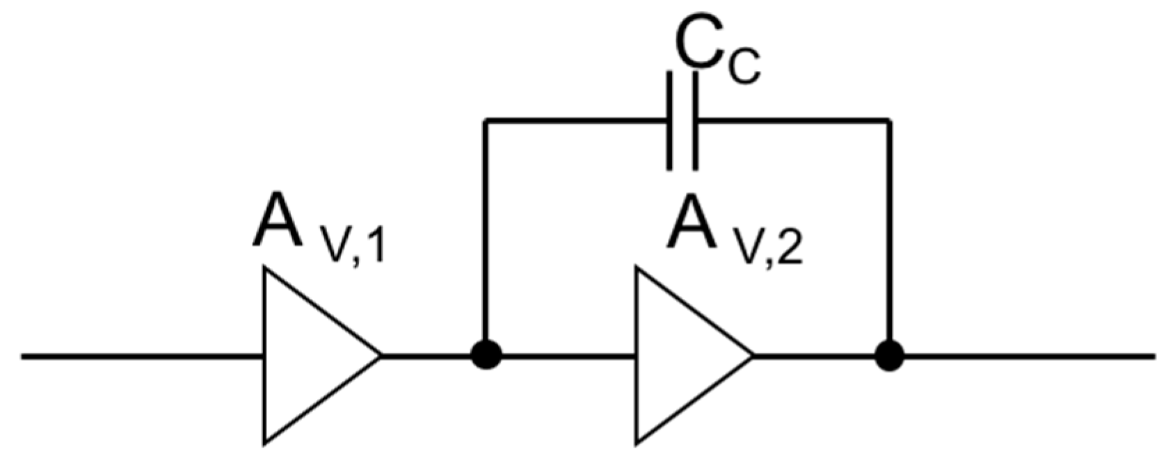
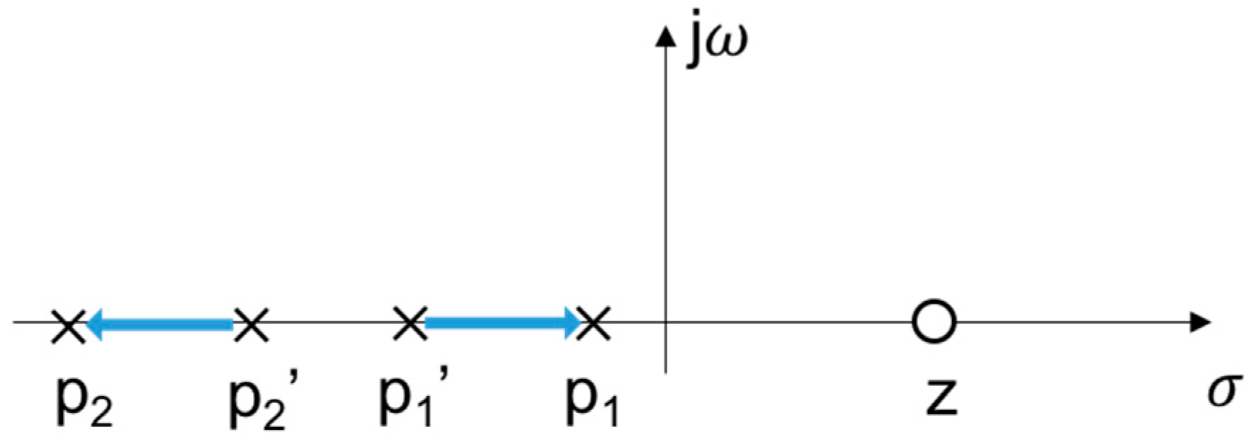
2.1.3. Stability Analysis
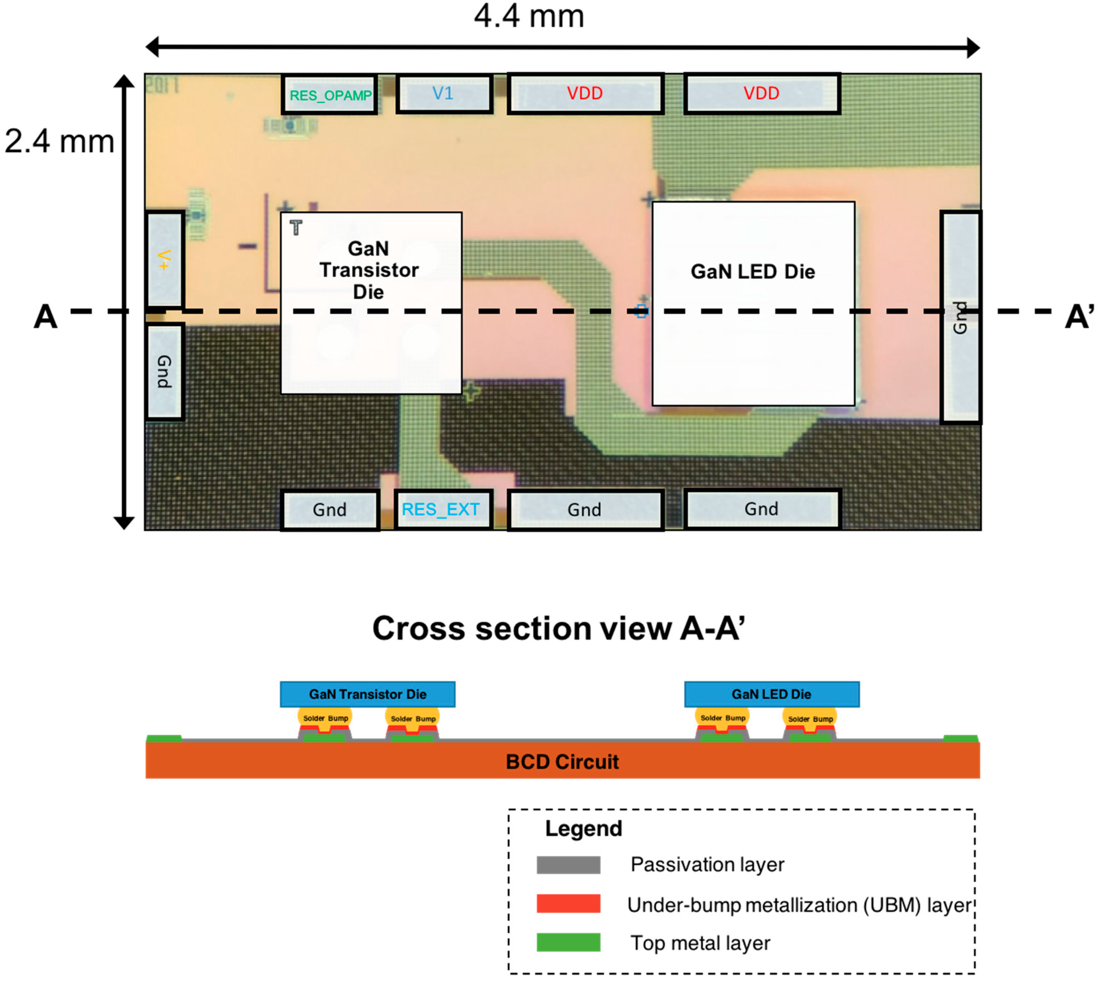
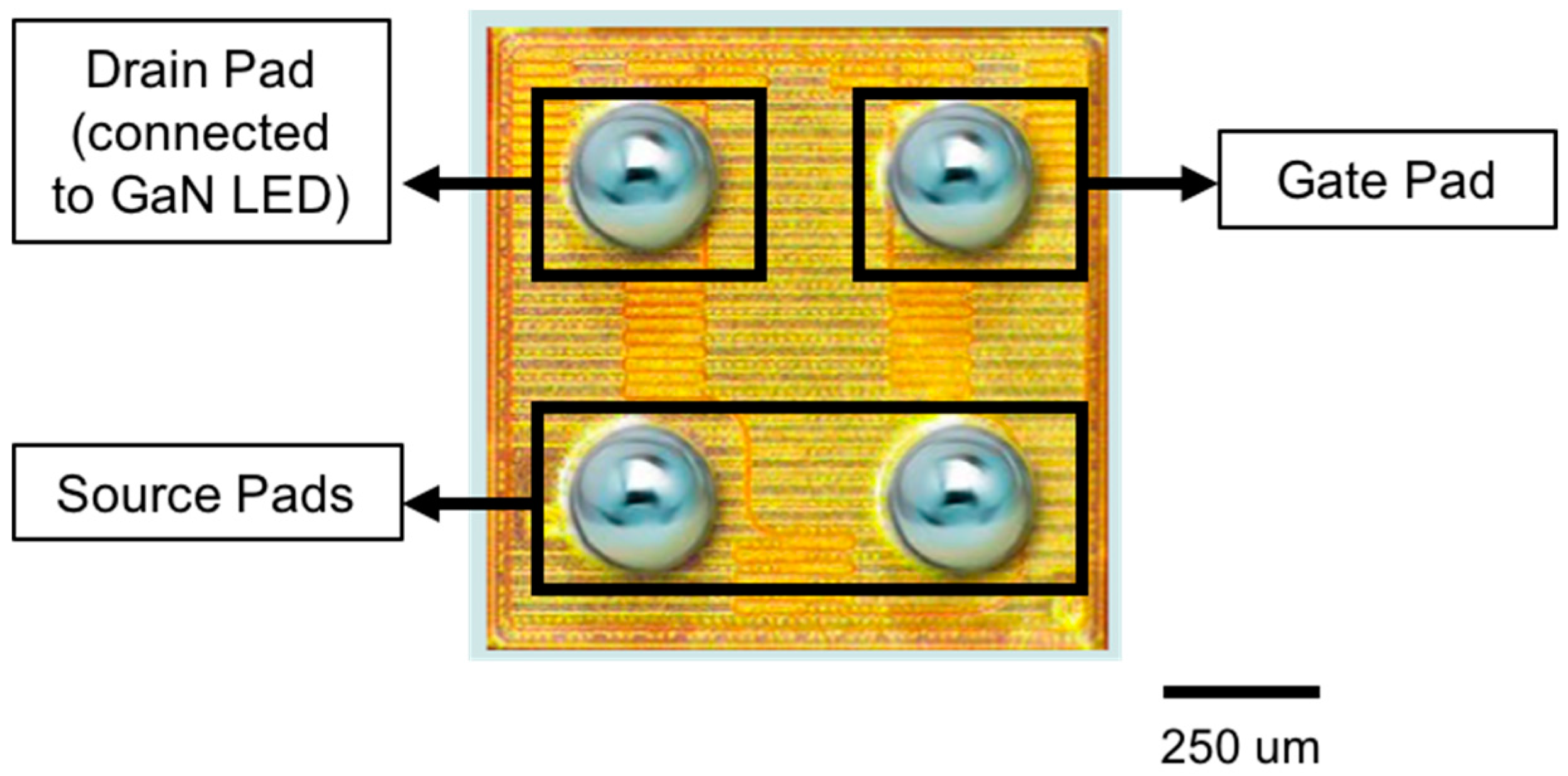
2.2. Assembly of GaN Transistor
2.3. Fabrication and Assembly of Custom GaN LED
2.4. Physical Implementation of Driver IC Using BCD Technology
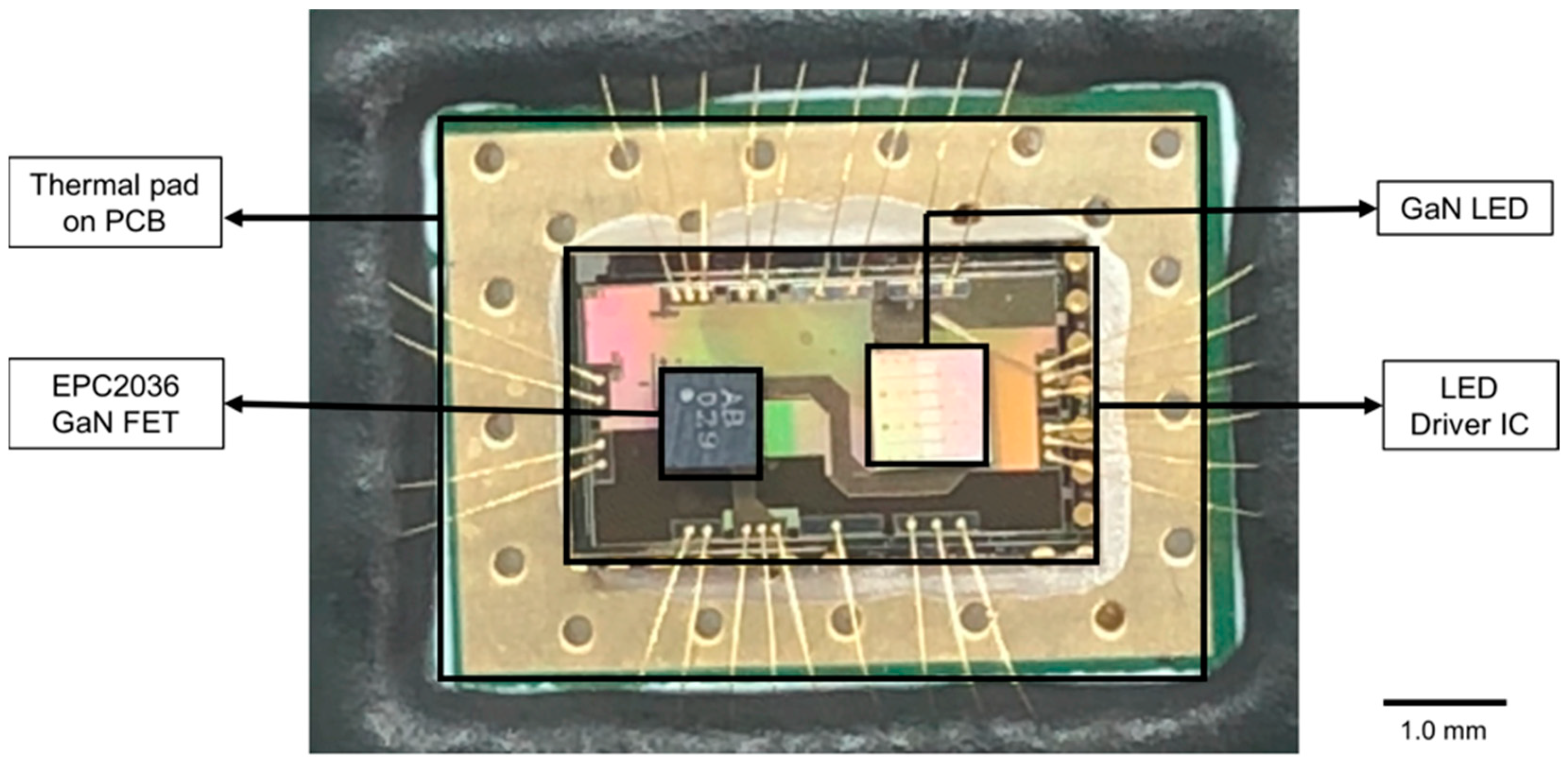
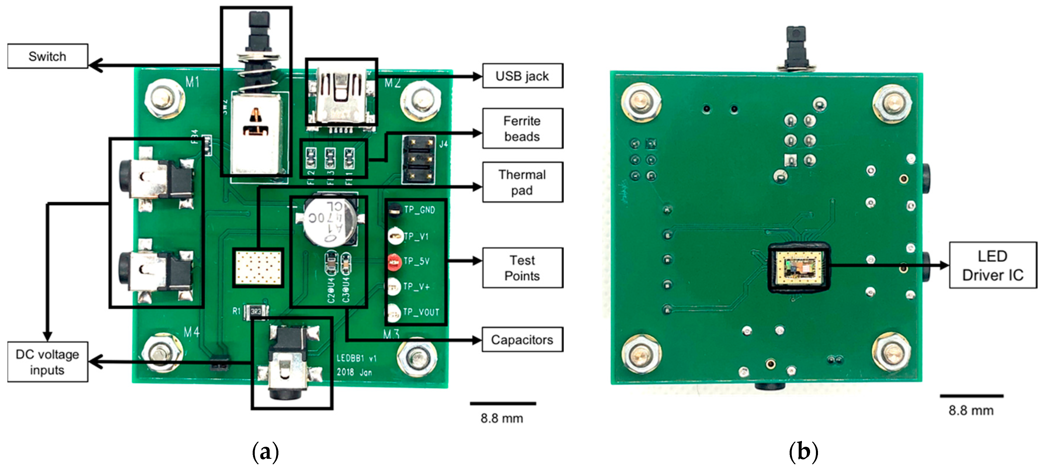
2.5. PCB Design and Prototype
3. Results
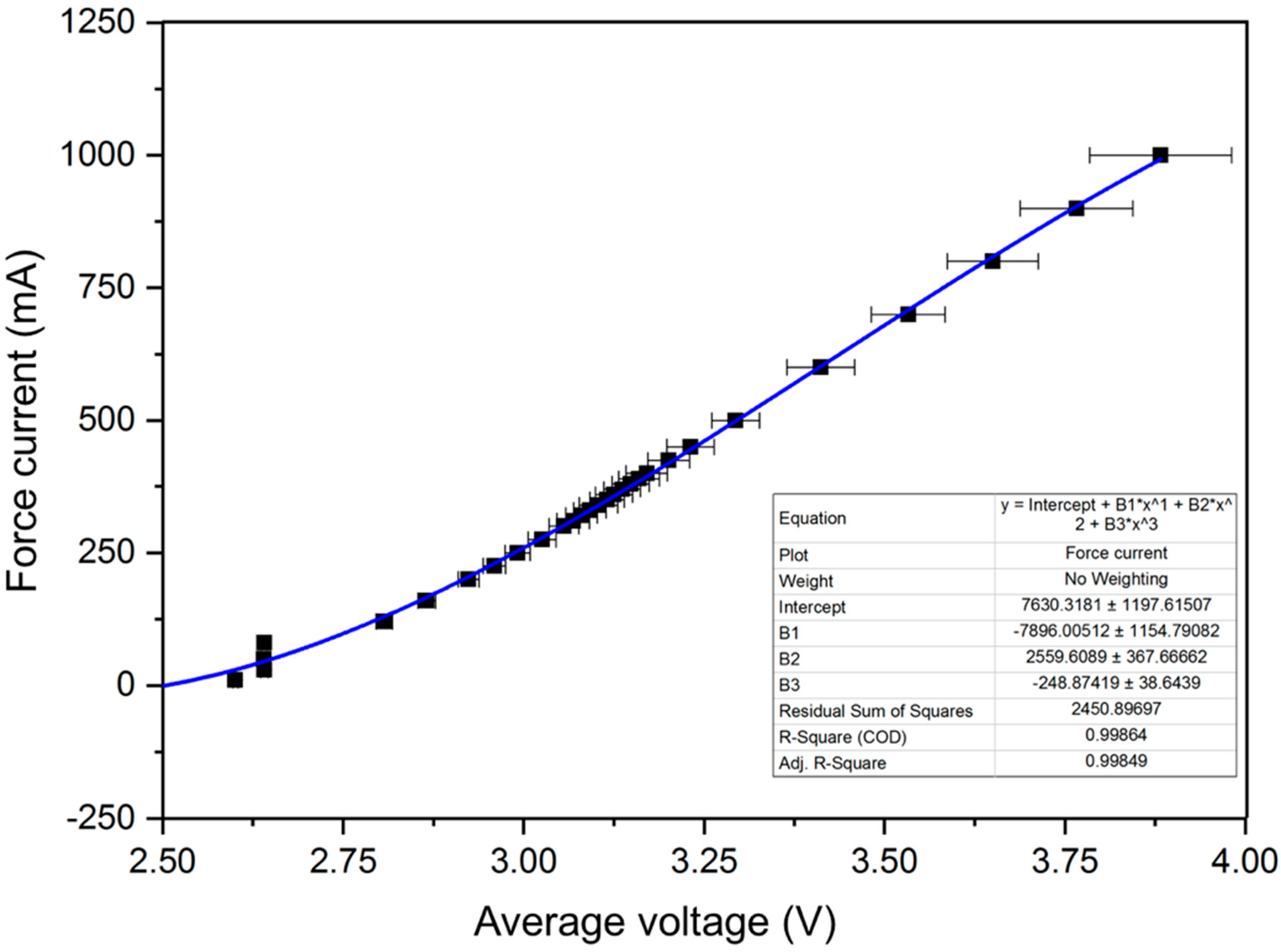
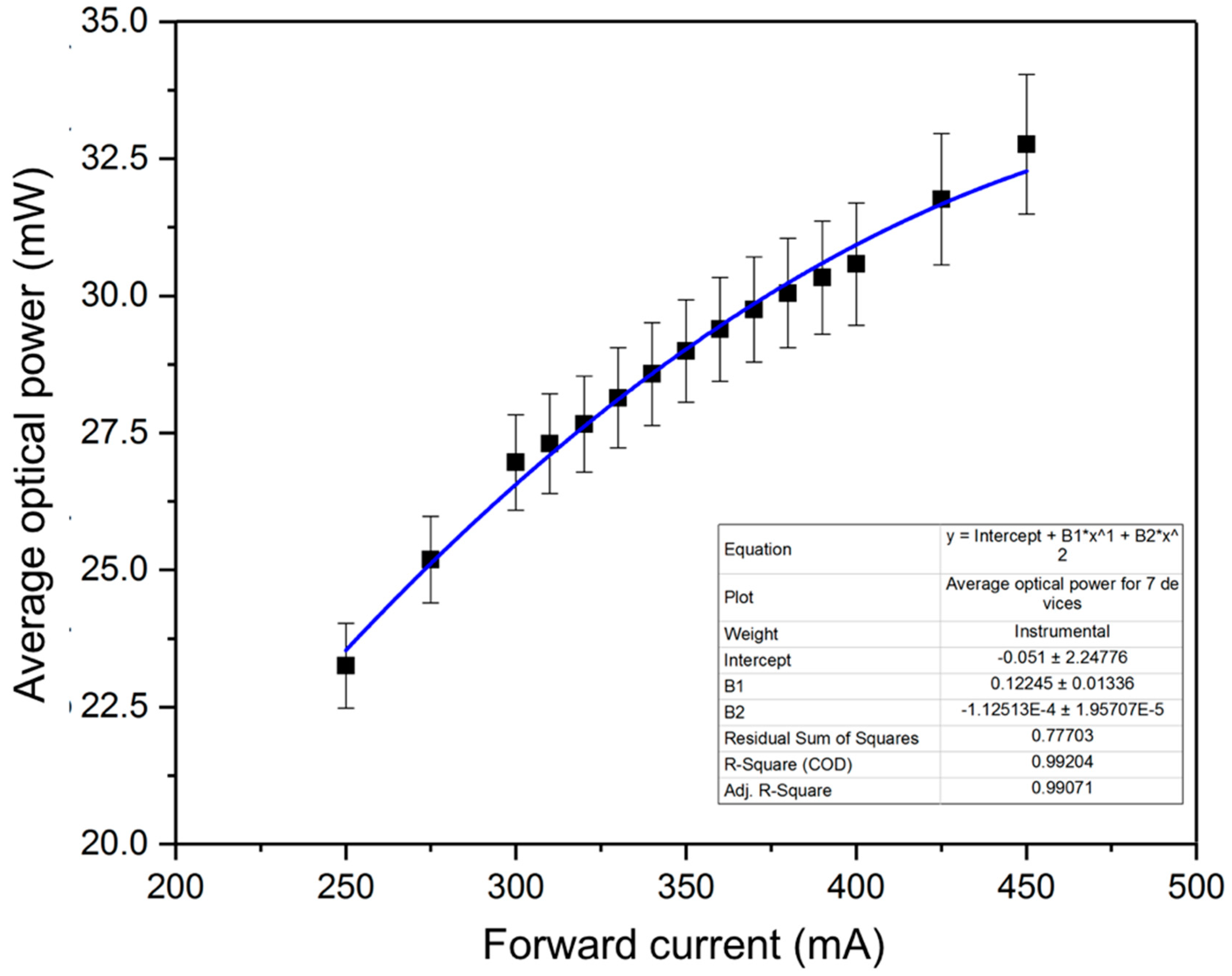
3.1. Functionality
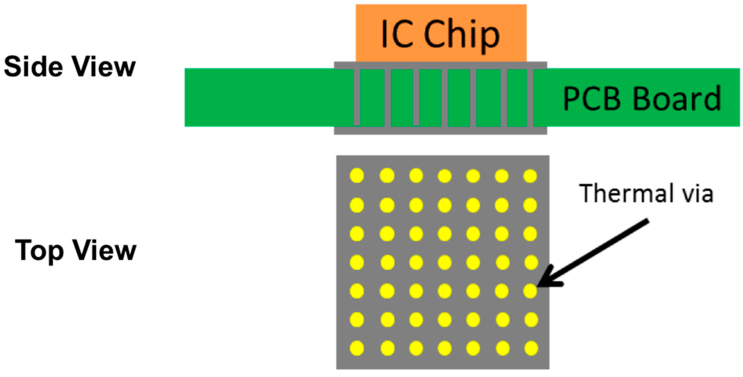
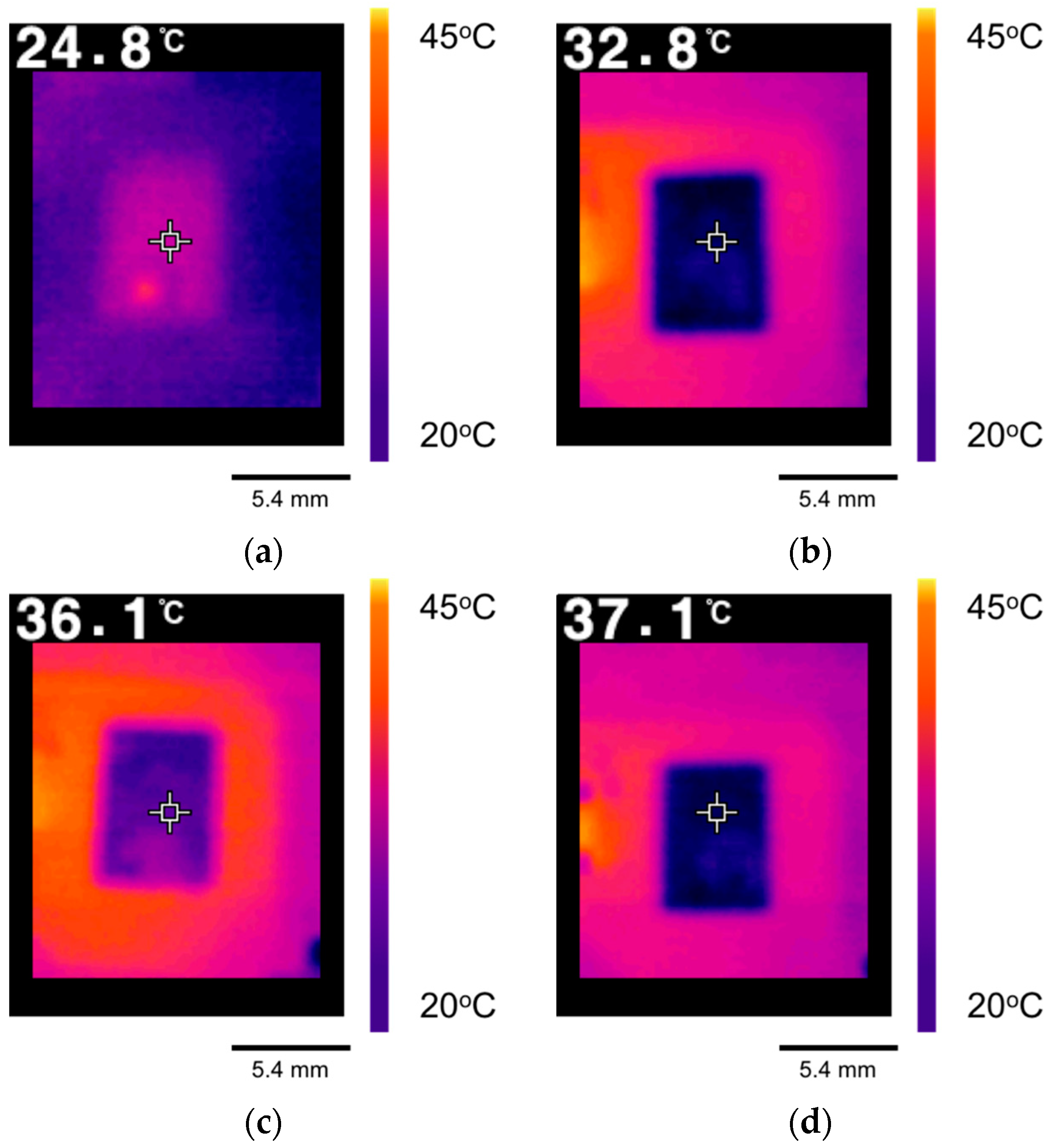
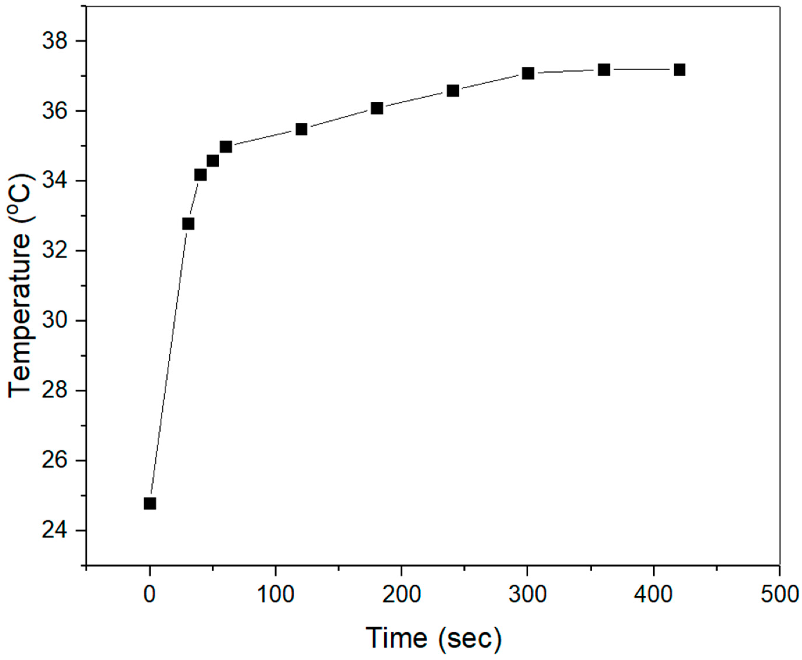
3.2. Thermal Testing
4. Discussion
5. Conclusions
Author Contributions
Funding
Acknowledgments
Conflicts of Interest
Abbreviations
| BCD | Bipolar CMOS DMOS |
| BEOL | Back End of Line |
| CFL | Compact Fluorescent Lights |
| CMOS | Complementary Metal Oxide Semiconductor |
| DAHI | Diverse Accessible Heterogeneous Integration |
| DARPA | Defense Advanced Research Projects Agency |
| DMOS | Double-Diffused Metal Oxide Semiconductor |
| FET | Field Effect Transistor |
| EDB | Economic Development Board |
| IC | Integrated Circuits |
| IO | Input/Output |
| IR | Infrared |
| KCL | Kirchhoff’s Current Law |
| LED | Light Emitting Diode |
| MCPCB | Metal-Core Printed Circuit Board |
| NTU | Nanyang Technological University |
| PCB | Printed Circuit Board |
| RF | Radio Frequency |
| SUTD | Singapore University of Technology and Design |
| UBM | Under-Bump Metallization |
References
- How Energy-Efficient Light Bulbs Compare with Traditional Incandescents. Available online: https://www.energy.gov/energysaver/save-electricity-and-fuel/lighting-choices-save-you-money/how-energy-efficient-light (accessed on 23 January 2017).
- Soh, M.Y.; Ng, W.X.; Zou, Q.; Lee, D.; Teo, T.H.; Yeo, K.S. Low-cost Real-time Video Streaming System Using Off-the-Shelf LEDs. In Proceedings of the IEEE Region 10 Conference (TENCON 2018), Jeju, Korea, 28–31 October 2018; pp. 1774–1777. [Google Scholar]
- Soh, M.Y.; Ng, W.X.; Zou, Q.; Lee, D.; Teo, T.H.; Yeo, K.S. Real-Time Audio Transmission Using Visible Light Communication. In Proceedings of the IEEE Region 10 Conference (TENCON 2018), Jeju, Korea, 28–31 October 2018; pp. 2223–2226. [Google Scholar]
- Chen, W.; Yu, C.; Kwok, Y.S.; Chin, F. Video transmission system based on visible light communication. In Proceedings of the 2011 IEEE International Conference on Information Photonics and Optical Communications (IPOC), Jurong West, Singapore, 21–23 October 2011; pp. 1–3. [Google Scholar]
- Khan, L.U. Visible light communication: Applications, architecture, standardization and research challenges. Digit. Commun. Netw. 2017, 3, 78–88. [Google Scholar] [CrossRef] [Green Version]
- Nagdev, J.; Sher, D.; Nathani, R.; Kalwani, G. Wireless Data Transfer Using Light Fidelity. Int. J. Sci. Res. (IJSR) 2013, 2, 106–108. [Google Scholar]
- Ohara, M.; Kawashima, Y.; Kitajima, S.; Mitsuoka, C.; Watanabe, H. Blue light inhibits the growth of skin tumors in the v-Ha-ras transgenic mouse. Cancer Sci. 2003, 94, 205–209. [Google Scholar] [CrossRef] [PubMed] [Green Version]
- Adamskaya, N.; Dungel, P.; Mittermayr, R.; Hartinger, J.; Feichtinger, G.; Wassermann, K.; Redl, H.; van Griensven, M. Light therapy by blue LED improves wound healing in an excision model in rats. Injury 2011, 42, 917–921. [Google Scholar] [CrossRef] [PubMed]
- Rossi, F.; Pini, R.; De Siena, G.; Massi, D.; Pavone, F.S.; Alfieri, D.; Cannarozzo, G. A blue-LED-based device for selective photocoagulation of superficial abrasions: Theoretical modeling and in vivo validation. In Proceedings of the Photonic Therapeutics and Diagnostics VI, San Jose, CA, USA, 23–25 January 2010. [Google Scholar]
- Brezinski, D.J. Portable Phototherapy Device. U.S. Patent 9604072B2, 28 March 2017. [Google Scholar]
- Soh, M.Y.; Teo, T.H.; Ng, W.X.; Yeo, K.S. Review of high efficiency integrated LED lighting. In Proceedings of the 2017 IEEE 12th International Conference on Power Electronics and Drive Systems (PEDS), Honolulu, HI, USA, 12–15 December 2017; pp. 93–97. [Google Scholar]
- Prendergast, P. How to Design a Three-Channel LED Driver. Cypress Perform 2008, 1–9. [Google Scholar]
- Tipirneni, N.; Koudymov, A.; Adivarahan, V.; Yang, J.; Simin, G.; Khan, M.A. The 1.6-kV AlGaN/GaN HFETs. IEEE Electron Device Lett. 2006, 27, 716–718. [Google Scholar] [CrossRef]
- Wu, Y.F.; Kapolnek, D.; Ibbetson, J.P.; Parikh, P.; Keller, B.P.; Mishra, U.K. Very-High Power Density AlGaN/GaN HEMTs. IEEE Trans. Electron Devices 2001, 48, 586–590. [Google Scholar]
- Kaminski, N. State of the art and the future of wide band-gap devices. In Proceedings of the IEEE 13th European Conference on Power Electronics and Applications, Barcelona, Spain, 8–10 September 2009; pp. 1–9. [Google Scholar]
- Wu, Y.F.; Moore, M.; Saxler, A.; Wisleder, T.; Parikh, P. 40-W/mm double field-plated GaN HEMTs. In Proceedings of the 2006 64th Device Research Conference, State College, PA, USA, 26–28 June 2006; pp. 151–152. [Google Scholar]
- Cree’s Silicon Carbide Schottky Diode Chip; CPW2-1200S050; Cree Inc.: Dehan, NC, USA, 2009.
- Green, D.S.; Dohrman, C.L.; Demmin, J.; Zheng, Y.; Chang, T.H. A Revolution on the Horizon from DARPA: Heterogeneous Integration for Revolutionary Microwaven/Millimeter-Wave Circuits at DARPA: Progress and Future Directions. IEEE Microw. Mag. 2017, 18, 44–59. [Google Scholar] [CrossRef]
- Raman, S.; Chang, T.H.; Dohrman, C.L.; Rosker, M.J. The DARPA COSMOS program: The convergence of InP and silicon CMOS technologies for high-performance mixed-signal. In Proceedings of the 2010 International Conference on Indium Phosphide & Related Materials (IPRM), Kagawa, Japan, 31 May–4 June 2010; pp. 1–5. [Google Scholar]
- Liu, M.J.; Hsu, S.S. A Miniature 300-MHz Resonant DC-DC Converter with GaN and CMOS Integrated in IPD Technology. IEEE Trans. Power Electron. 2018, 33, 9656–9668. [Google Scholar] [CrossRef]
- Aklimi, E. Magnetics and GaN for Integrated CMOS Voltage Regulators. Ph.D. Thesis, Columbia University, New York, NY, USA, 2016. [Google Scholar]
- Gutierrez-Aitken, A.; Chang-Chien, P.; Scott, D.; Hennig, K.; Kaneshiro, E.; Nam, P.; Cohen, N.; Ching, D.; Thai, K.; Oyama, B.; et al. Advanced heterogeneous integration of InP HBT and CMOS Si technologies. In Proceedings of the 2010 IEEE Compound Semiconductor Integrated Circuit Symposium (CSICS), Monterey, CA, USA, 3–6 October 2010; pp. 1–4. [Google Scholar]
- Oyama, B.; Ching, D.; Thai, K.; Gutierrez-Aitken, A.; Patel, V.J. InP HBT/Si CMOS-based 13-b 1.33-Gsps digital-to-analog converter with> 70-dB SFDR. IEEE J. Solid-State Circuits 2013, 48, 2265–2272. [Google Scholar] [CrossRef]
- Raman, S.; Dohrman, C.L.; Chang, T.H. The DARPA diverse accessible heterogeneous integration (DAHI) program: Convergence of compound semiconductor devices and silicon-enabled architectures. In Proceedings of the 2012 IEEE International Symposium on Radio-Frequency Integration Technology (RFIT), Singapore, 21–23 November 2012; pp. 1–6. [Google Scholar]
- Aklimi, E.; Piedra, D.; Tien, K.; Palacios, T.; Shepard, K.L. Hybrid CMOS/GaN 40-MHz maximum 20-V input DC–DC multiphase buck converter. IEEE J. Solid-State Circuits 2017, 52, 1618–1627. [Google Scholar] [CrossRef]
- Meng, F.; Disney, D.; Liu, B.; Volkan, B.; Zhou, A.; Liang, Z.; Yi, X.; Selvaraj, L.; Peng, L.; Ma, K.; et al. Heterogeneous Integration of GaN and BCD Technologies and Its Applications to High Conversion-ratio DC-DC Boost Converter IC. IEEE Trans. Power Electron. 2018, 34, 1993–1996. [Google Scholar] [CrossRef]
- Yang, Y.Y.; Wang, S.W.; Hsieh, C.Y.; Huang, T.C.; Lee, Y.H.; Chen, K.H. Power Management With a Low-Ripple High-Conversion-Ratio 80-V Output Voltage Boost Converter for Avalanche Photodiode System. IEEE Trans. Ind. Electron. 2013, 60, 2627–2637. [Google Scholar] [CrossRef]
- Selvaraj, S.L.; Peng, L.; Qiong, Z.; Seng, Y.K.; Disney, D. Heterogeneous Integration of GaN LED on CMOS Driver Circuit for Mobile Phone Applications. In Proceedings of the 2018 IEEE 2nd Electron Devices Technology and Manufacturing Conference (EDTM), Kobe, Japan, 13–16 March 2018; pp. 71–73. [Google Scholar]
- Johns, D.A.; Martin, K. Analog Integrated Circuit Design; John Wiley & Sons: Hoboken, NJ, USA, 2008. [Google Scholar]
- Putra, A.; Teo, T.H.; Rajinder, S. Ultra-Low-Power Low-Voltage Integrated Preamplifier Using Class-AB Op-Amp for Biomedical Sensor Application. In Proceedings of the 2007 International Symposium on Integrated Circuits, Singapore, 26–28 September 2007; pp. 216–219. [Google Scholar]
- Lim, G.K.; Teo, T.H. A Low-Power Low-Voltage Amplifier for Heart Rate Sensor. In Proceedings of the 2006 IEEE Asia Pacific Conference on Circuits and Systems (APCCAS), Singapore, 4–7 December 2006; pp. 502–505. [Google Scholar]
- fficient Power Conversion (EPC) Corporation. EPC2036—Enhancement Mode Power Transistor; EPC Coporation: El Segundo, CA, USA, May 2018. [Google Scholar]
- Li, X.; Wu, L.; Liu, Z.; Hussain, B.; Chong, W.C.; Lau, K.M.; Yue, C.P. Design and characterization of active matrix LED microdisplays with embedded visible light communication transmitter. J. Lightwave Technol. 2016, 34, 3449–3457. [Google Scholar] [CrossRef]
- McKendry, J.J.; Rae, B.R.; Gong, Z.; Muir, K.R.; Guilhabert, B.; Massoubre, D.; Gu, E.; Renshaw, D.; Dawson, M.D.; Henderson, R.K. Individually addressable AlInGaN micro-LED arrays with CMOS control and subnanosecond output pulses. IEEE Photonics Technol. Lett. 2009, 21, 811–813. [Google Scholar] [CrossRef]
- Jang, S.Y.; Wolf, J.; Ehrmann, O.; Gloor, H.; Schreiber, T.; Reichl, H.; Paik, K.W. CrCu based UBM (under bump metallization) study with electroplated Pb/63Sn solder bumps-interfacial reaction and bump shear strength. IEEE Trans. Compon. Packag. Technol. 2003, 26, 245–254. [Google Scholar] [CrossRef]
- VARTA; VARTA Consumer Batteries GmbH Co.; KGaA. V4903 Datasheet—Farnell Element14; VARTA: Ellwangen, Germany, 2005. [Google Scholar]
- Battery Life Calculator|DigiKey Electronics. Available online: https://www.digikey.com/en/resources/conversion-calculators/conversion-calculator-battery-life (accessed on 12 March 2019).
- FLIR. FLIR TG165 Imaging IR Thermometer; FLIR: Wilsonville, OR, USA, January 2017. [Google Scholar]
- Thermocouple Thermometer with Four Type K/J Inputs and Data Logging Model 20250-03. Available online: https://pim-resources.coleparmer.com/instruction-manual/20250-03.pdf (accessed on 12 March 2019).
- Digi-Key. How to Measure the Unknown Thermal Emissivity of Objects/Materials Using the U5855A TrueIR Thermal Imager (Application Note); Digi-Key: Thief River Falls, MN, USA, 2015. [Google Scholar]
- International Electrotechnical Commission. Information Technology Equipment-Safety—Part 1: General Requirements [IEC 60950–1-Ed. 1]; International Electrotechnical Commission: Geneva, Switzerland, 2001. [Google Scholar]
- Shen, J.; Wu, Y.; Liu, T.; Zheng, Q. Constant current LED driver based on flyback structure with primary side control. In Proceedings of the 2011 IEEE Power Engineering and Automation Conference, Wuhan, China, 8–9 September 2011; Volume 1, pp. 260–263. [Google Scholar]
- Fan, Y.H.; Wu, C.J.; Fan, C.C.; Chih, K.W.; Liao, L.D. A simplified LED converter design and implement. In Proceedings of the 9th Joint International Conference on Information Sciences (JCIS-06); Atlantis Press: Paris, France, 2006. [Google Scholar]
- Philips. LED Driver Outdoor 12W/0.35A-33V 230V; Philips: Amsterdam, The Netherlands, 2006. [Google Scholar]
- Horng, R.H.; Hong, J.S.; Tsai, Y.L.; Wuu, D.S.; Chen, C.M.; Chen, C.J. Optimized thermal management from a chip to a heat sink for high-power GaN-based light-emitting diodes. IEEE Trans. Electron Devices 2010, 57, 2203–2207. [Google Scholar] [CrossRef]
- Tabisz, W.A.; Gradzki, P.M.; Lee, F.C. Zero-voltage-switched quasi-resonant buck and flyback converters-experimental results at 10 MHz. IEEE Trans. Power Electron. 1989, 4, 194–204. [Google Scholar] [CrossRef]
- Bandyopadhyay, S.; Neidorff, B.; Freeman, D.; Chandrakasan, A.P. 90.6% Efficient 11 MHz 22 W LED driver Using GaN FETs And Burst-Mode Controller With 0.96 Power Factor. In Proceedings of the 2013 IEEE International Solid-State Circuits Conference Digest of Technical Papers, San Francisco, CA, USA, 17–21 February 2013; pp. 368–369. [Google Scholar]


© 2019 by the authors. Licensee MDPI, Basel, Switzerland. This article is an open access article distributed under the terms and conditions of the Creative Commons Attribution (CC BY) license (http://creativecommons.org/licenses/by/4.0/).
Share and Cite
Soh, M.Y.; Teo, T.H.; Selvaraj, S.L.; Peng, L.; Disney, D.; Yeo, K.S. Heterogeneous Integration of GaN and BCD Technologies. Electronics 2019, 8, 351. https://doi.org/10.3390/electronics8030351
Soh MY, Teo TH, Selvaraj SL, Peng L, Disney D, Yeo KS. Heterogeneous Integration of GaN and BCD Technologies. Electronics. 2019; 8(3):351. https://doi.org/10.3390/electronics8030351
Chicago/Turabian StyleSoh, Mei Yu, T. Hui Teo, S. Lawrence Selvaraj, Lulu Peng, Don Disney, and Kiat Seng Yeo. 2019. "Heterogeneous Integration of GaN and BCD Technologies" Electronics 8, no. 3: 351. https://doi.org/10.3390/electronics8030351