A 2.5 Gbps, 10-Lane, Low-Power, LVDS Transceiver in 28 nm CMOS Technology


Abstract
:1. Introduction
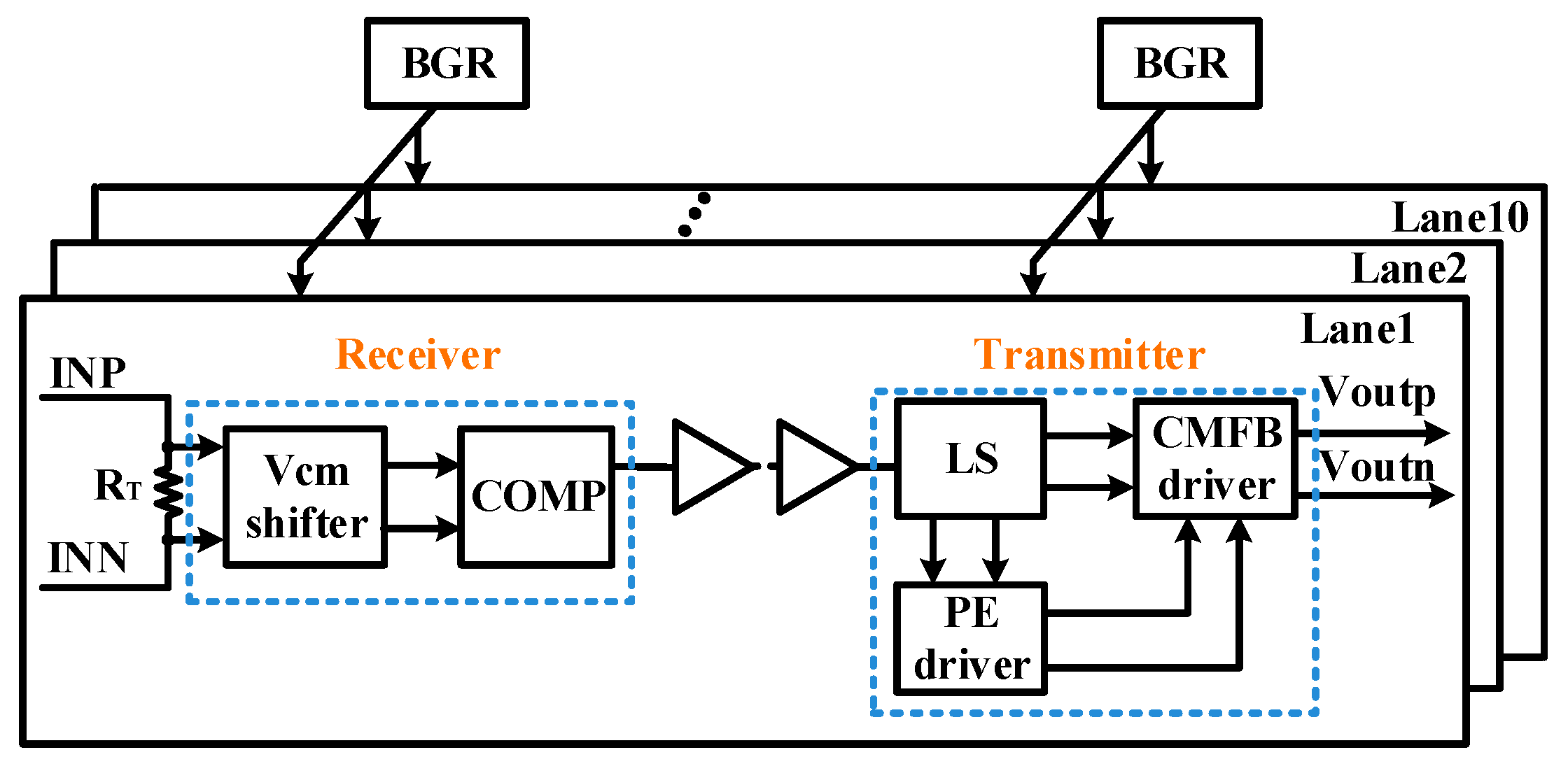
2. Architecture Design
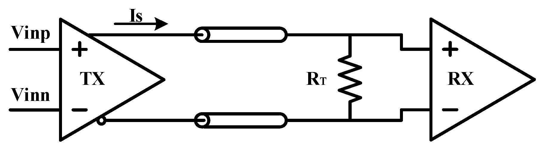
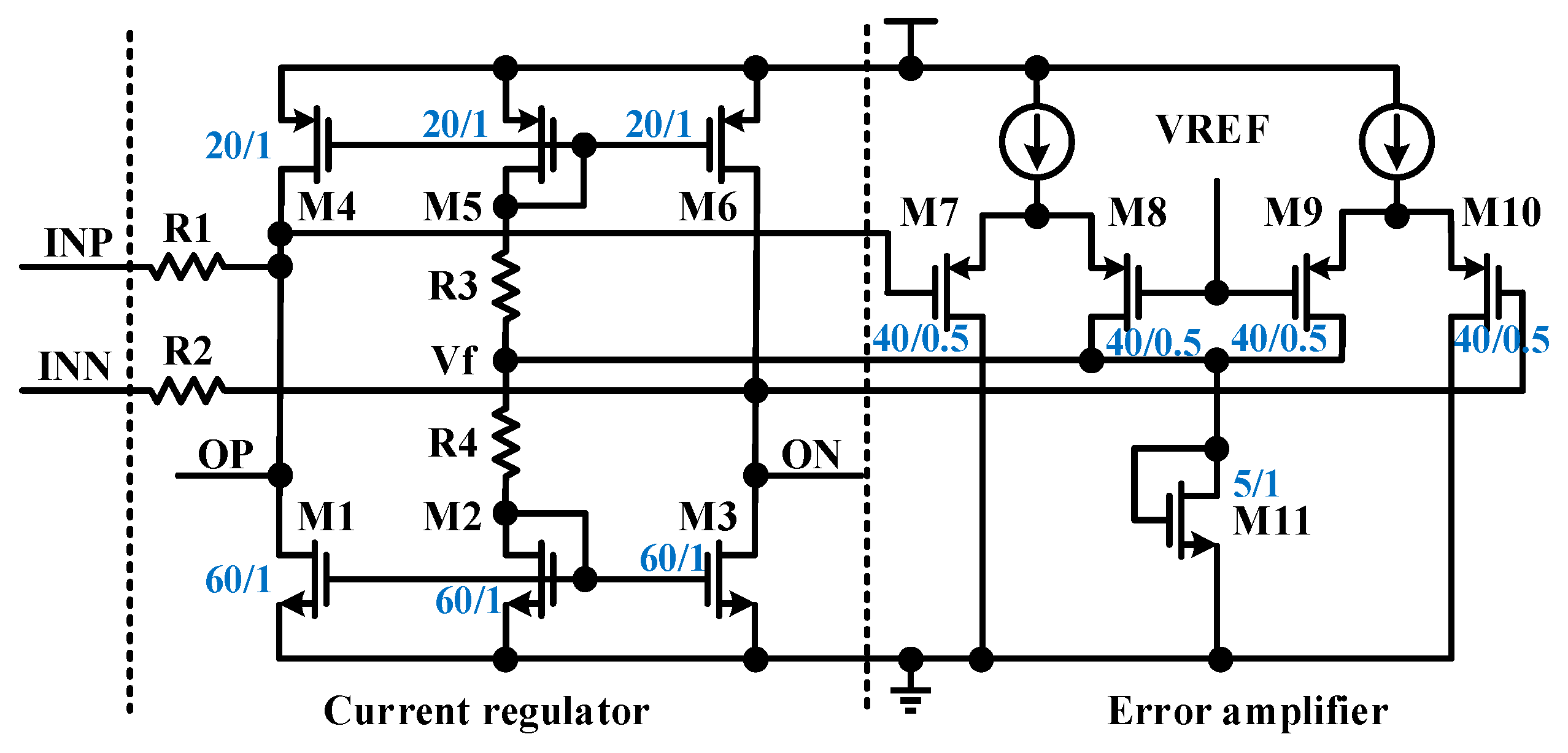
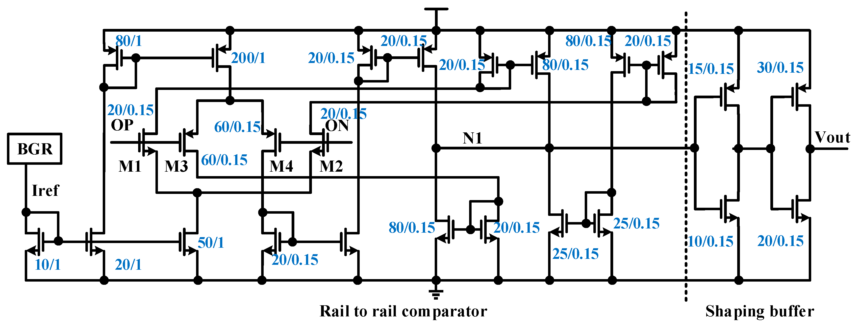
2.1. Receiver
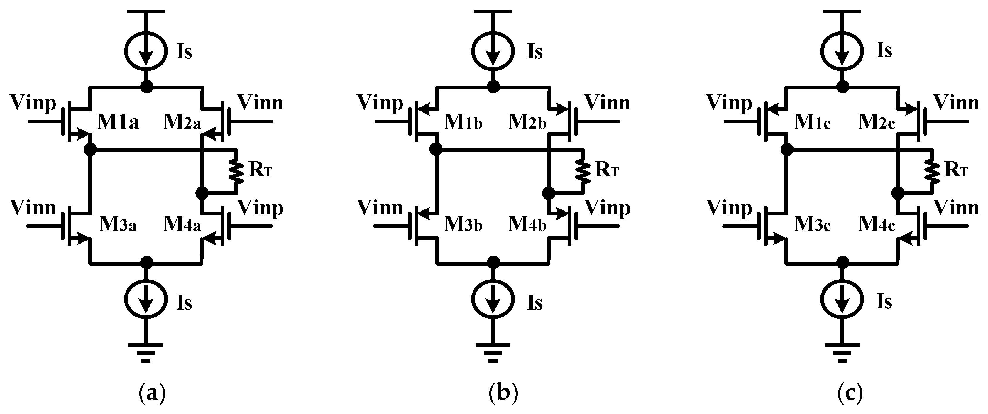
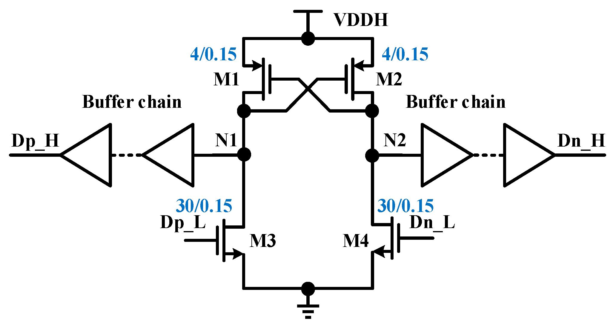
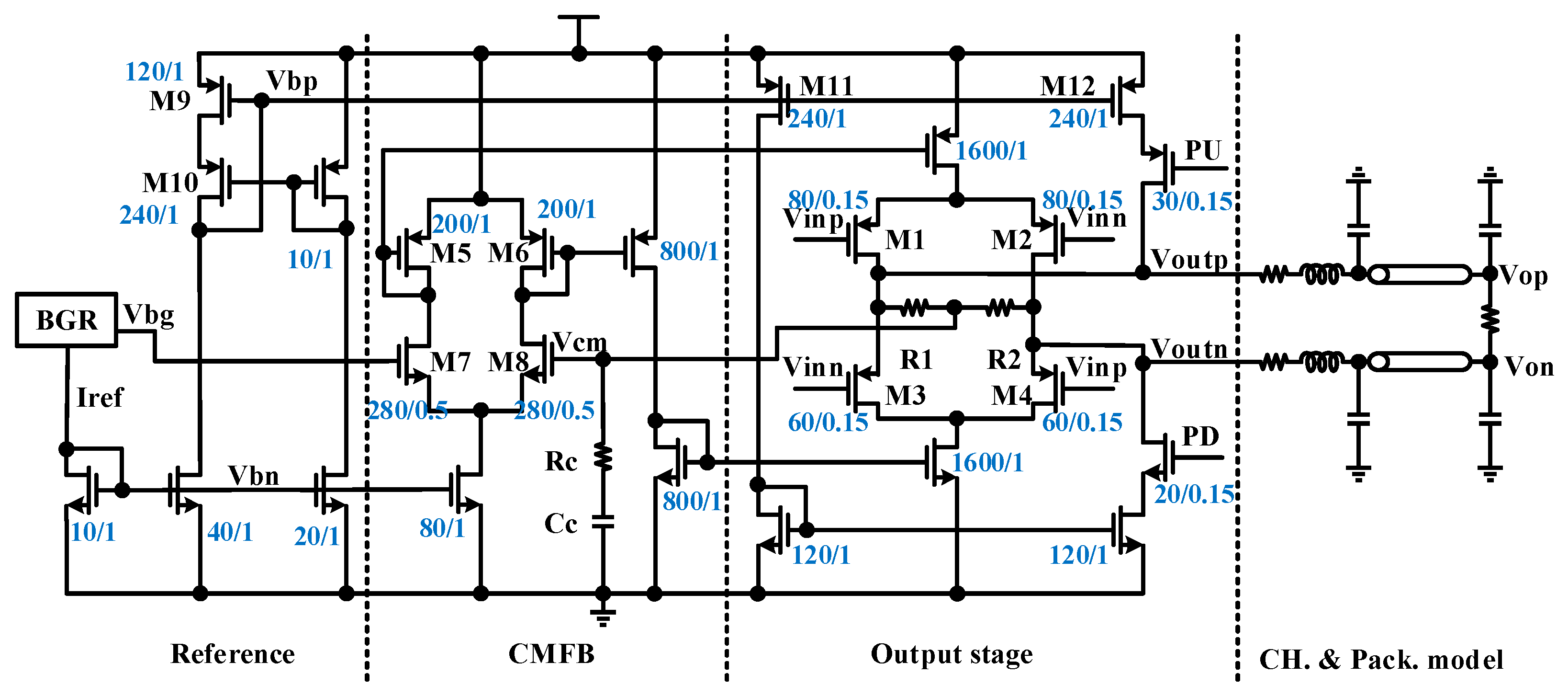
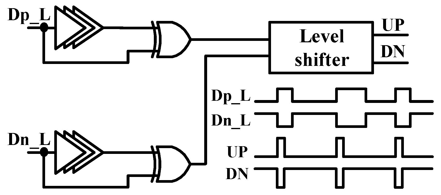
2.2. Transmitter
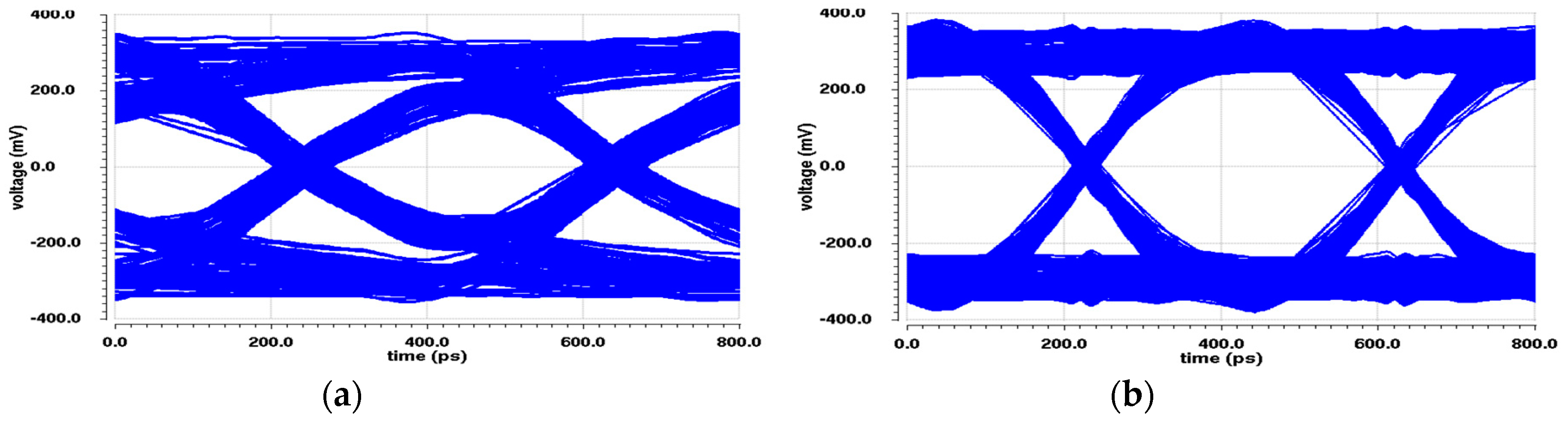
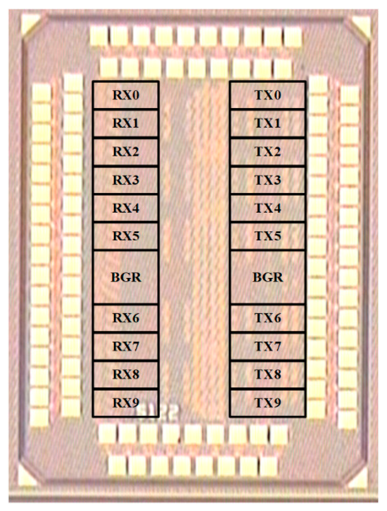
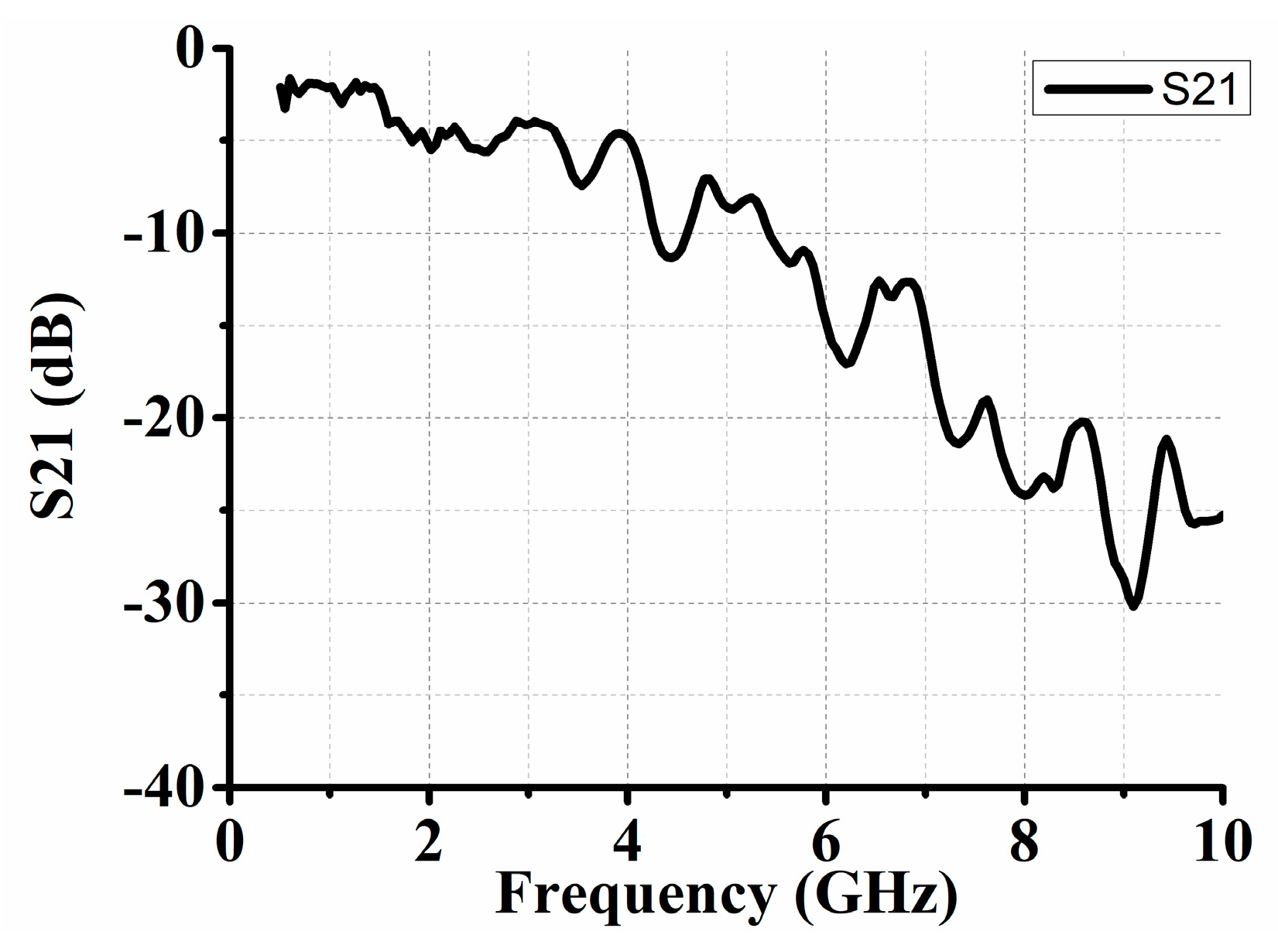
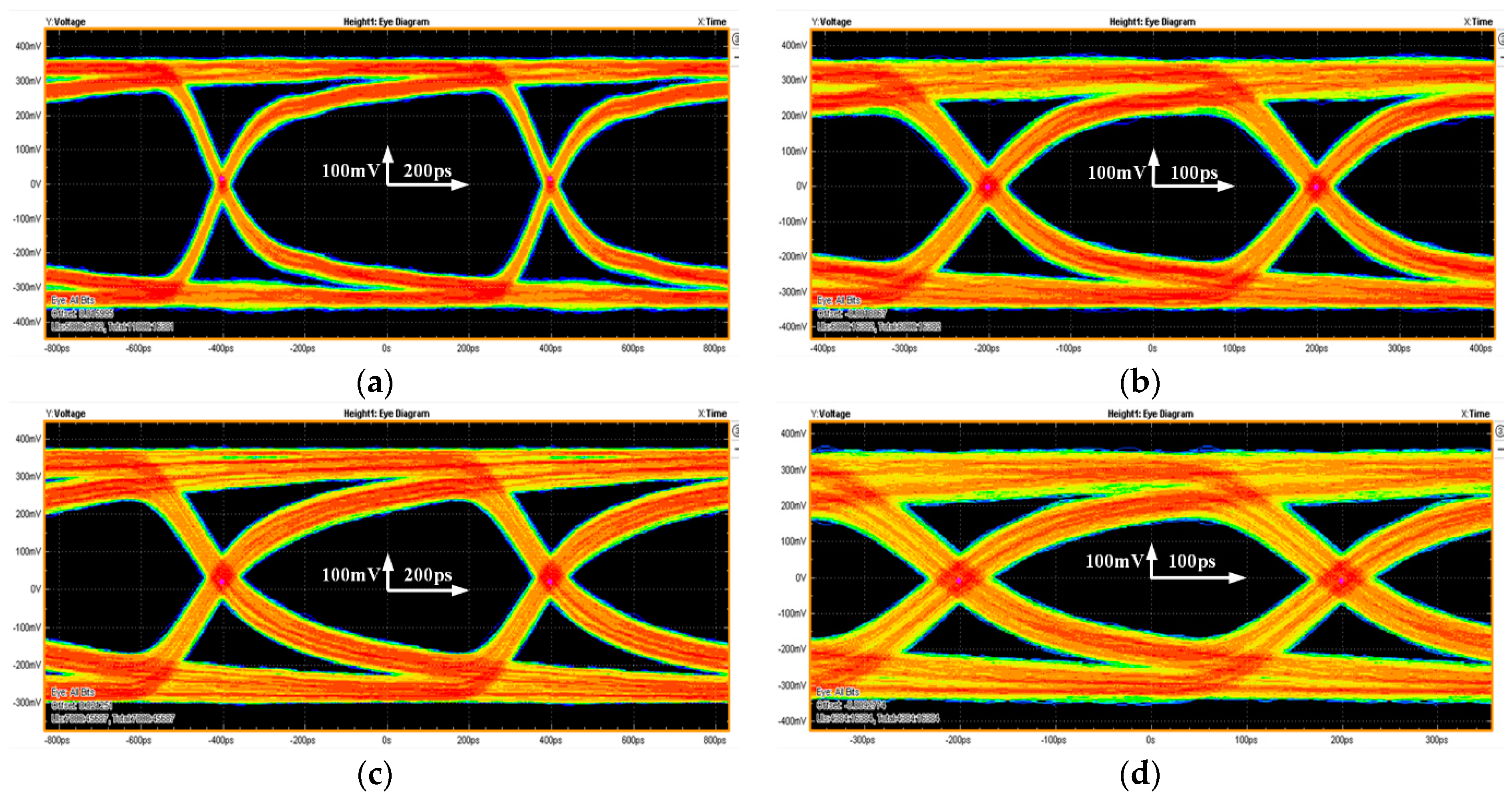
3. Measured Result Analysis and Discussion
4. Conclusions
Author Contributions
Funding
Acknowledgments
Conflicts of Interest
References
- Park, J.; Chae, J.H.; Jeong, Y.U.; Lee, J.W.; Kim, S. A 2.1-Gb/s 12-channel transmitter with phase emphasis embedded serializer for 55-in UHD intra-panel interface. IEEE J. Solid-State Circuits 2018, 53, 2878–2888. [Google Scholar] [CrossRef]
- Yousefzadeh, A.; Jabłoński, M.; Iakymchuk, T.; Linares-Barranco, A.; Rosado, A.; Plana, L.A.; Temple, S.; Serrano-Gotarredona, T.; Furber, S.B.; Linares-Barranco, B. On multiple AER handshaking channels over high-speed bit-serial bidirectional LVDS links with flow-control and clock-correction on commercial FPGAs for scalable neuromorphic systems. IEEE Trans. Biomed. Circuits Syst. 2017, 11, 1133–1147. [Google Scholar] [CrossRef] [PubMed]
- Jiang, B.J.; Pan, Z.B.; Qiu, Y.H. Study on the key technologies of a high-speed CMOS camera. Optik-Int. J. Light Electron Opt. 2017, 129, 100–107. [Google Scholar] [CrossRef]
- Shi, Z.; Tang, Z.A.; Feng, C.; Cai, H. Improvement to the signaling interface for CMOS pixel sensors. Nuclear Instrum. Methods Phys. Res. Sect. A Accel. Spectrometers Detect. Assoc. Equip. 2016, 832, 77–84. [Google Scholar] [CrossRef]
- Jayshree; Verma, S.; Chatterjee, A. A methodology for designing LVDS interface system. In Proceedings of the IEEE Sixth International Symposium on Embedded Computing and System Design, Patna, India, 15–17 December 2016; pp. 284–288. [Google Scholar] [CrossRef]
- Gilbert, A.; Mehmet, R.Y.; Jean-Michel, R. An integrated LVDS transmitter-receiver system with increased self-immunity to EMI in 0.18-μm CMOS. IEEE Trans. Electromagn. Compat. 2016, 58, 231–240. [Google Scholar] [CrossRef]
- Gupta, H.S.; Hari, S.G.; Parmar, R.M.; Dave, R.K. High speed LVDS driver for serdes. In Proceedings of the IEEE International Conference on Emerging Trends in Electronic and Photonic Devices & Systems, Varanasi, India, 22–24 December 2009; pp. 92–95. [Google Scholar] [CrossRef]
- Ning, H.W.; Zhen, G.Y.; Ren, Y.F. An optimal design of LVDS interface. In Proceedings of the IEEE International Conference on Computer Science and Network Technology, Harbin, China, 24–26 December 2011; pp. 2024–2026. [Google Scholar] [CrossRef]
- Graceffe, G.A.; Gatti, U.; Calligaro, C. A 400 Mbps radiation hardened by design LVDS compliant driver and receiver. In Proceedings of the IEEE International Conference on Electronics, Circuits and Systems, Bordeaux, France, 11–14 December 2016; pp. 109–112. [Google Scholar] [CrossRef]
- Sun, Z.Y.; Zhang, D.; Fang, W. A ASIC chip with pipeline ADCs for CCD sensor imaging system. Sens. Actuators A Phys. 2018, 279, 284–292. [Google Scholar] [CrossRef]
- Xu, H.Y.; Wang, J.; Lai, J.M. Design of a power efficient self-adaptive LVDS driver. IEICE Electron. Express 2018, 15. [Google Scholar] [CrossRef]
- Li, S.; Zhang, Q.; Zhao, X.; Liu, S.; Yuan, Z.; Zhang, X. Dynamic data transmission technology for expendable current profiler based on low-voltage differential signaling. Geosci. Instrum. Methods Data Syst. 2017, 6, 263–267. [Google Scholar] [CrossRef] [Green Version]
- Marar, H.W.; Abugharbieh, K.; Al-Tamimi, A.K. A power efficient 3 Gbps 1.8 V PMOS-based LVDS output driver. In Proceedings of the 19th IEEE International Conference on Electronics, Circuits, and Systems, Seville, Spain, 9–12 December 2012; pp. 240–243. [Google Scholar] [CrossRef]
- Traversi, G.; De Canio, F.; Liberali, V.; Stabile, A. Design of LVDS driver and receiver in 28 nm CMOS technology for associative memories. In Proceedings of the IEEE International Conference on Modern Circuits and Systems Technology, Thessaloniki, Greece, 4–6 May 2017; pp. 1–4. [Google Scholar] [CrossRef]
- Lv, J.; Ju, H.; Yuan, L.; Zhao, J.; Zhang, F.; Wu, B.; Jiang, J.; Zhou, Y. A high speed low jitter LVDS output driver for serial links. Analog Intergr. Circuits Signal Process. 2011, 68, 387–395. [Google Scholar] [CrossRef]
- Chen, M.; Silva-Martinez, J.; Nix, M.; Robinson, M.E. Low-voltage low-power LVDS drivers. IEEE J. Solid-State Circuits 2005, 40, 472–479. [Google Scholar] [CrossRef] [Green Version]
- Lee, S.S.; Lee, L.; Kung, F.W.; Saad, A.; Tan, G.H. A fully integrated and high precision 350 mV amplitude regulated LVDS transmitter compensating PVT variations. Microelectron. J. 2018, 81, 192–199. [Google Scholar] [CrossRef]
- Telecommunications Industry Association. Electrical Characteristics of Low Voltage Differential Signaling (LVDS) Interface Circuits; Standard ANSI/TIA/EIA-644-A (2001); Telecommunications Industry Association: Arlington, VA, USA, 1996. [Google Scholar]
- Louis, L.; John, C.; Jeffrey, D. A continuous-time common-mode feedback circuit (CMFB) for high-impedance current-mode applications. IEEE Trans. Circuit Syst. II Analog Digit. Signal Process. 2000, 47, 363–369. [Google Scholar] [CrossRef]
- Divide, M.; Gaetano, P.; Salvatore, P. A new compact low-power high-speed rail-to-rail Class-B buffer for LCD applications. J. Disp. Technol. 2010, 6, 184–190. [Google Scholar] [CrossRef]
- Nagy, L.; Arbet, D.; Kovac, M.; Potocny, M.; Stopjakova, V. Design and performance analysis of ultra-low voltage rail-to-rail comparator in 130 nm CMOS technology. In Proceedings of the IEEE 21st International Symposium on Design and Diagnostics of Electronic Circuits and Systems, Budapest, Hungary, 25–27 April 2018; pp. 51–54. [Google Scholar] [CrossRef]
- Priti, G.; Ujwala, G. Design of voltage level shifter for multi-supply voltage design. In Proceedings of the International Conference on Communication and Signal Processing, Melmaruvathur, India, 6–8 April 2016; pp. 853–857. [Google Scholar] [CrossRef]
- Lanuzza, M.; Corsonello, P.; Perri, S. Low-Power Level Shifter for Multi-Supply Voltage Designs. IEEE Trans. Circuits Syst. II Express Briefs 2012, 59, 922–926. [Google Scholar] [CrossRef]
- Ahmed, N.; Edgar, S.-S.; Jose, S.-M. A fully balanced pseudo-differential OTA with common mode feedback and inherent common mode detector. IEEE J. Solid-State Circuits 2003, 38, 663–668. [Google Scholar] [CrossRef]
- Basu, J.; Mandal, P. Effect of switched-capacitor CMFB on the gain of fully differential OP-Amp for design of integrators. In Proceedings of the IEEE International Symposium on Circuits and System, Florence, Italy, 27–30 May 2018; pp. 1–5. [Google Scholar] [CrossRef]
- Ševčík, B.; Brančík, L. Time-domain pre-emphasis technique based on pulse-width modulation scheme. In Proceedings of the IEEE International Conference on Telecommunications and Signal Processing, Budapest, Hungary, 18–20 August 2011; pp. 483–486. [Google Scholar] [CrossRef]
- Gilbert, A.; Huang, H.Y. Equalization and pre-emphasis based LVDS transceiver. Analog Intergr. Circ. Signal Process. 2013, 75, 109–123. [Google Scholar] [CrossRef]
- Jawed, S.A.; Asghar, A.; Khan, K.; Abbasi, S.; Naveed, M.; Siddiqi, Y.; Siddiqi, W. A configurable 2-Gbps LVDS transceiver in 150-nm CMOS with pre-emphasis, equalization, and slew rate control. Int. J. Circuit Theory Appl. 2017, 45, 1369–1381. [Google Scholar] [CrossRef]
- Xu, Y.; Sun, T.Q.; Zhao, F.; Hu, C. A full-integrated LVDS transceiver in 0.5 μm CMOS technology. In Proceedings of the IEEE Conference on Industrial Electronics and Applications, Hangzhou, China, 9–11 June 2014; pp. 1672–1675. [Google Scholar] [CrossRef]
- Ayyagari, R.; Gopal, K. Low power LVDS transmitter design and analysis. In Proceedings of the IEEE The Asia-Pacific Conference on Communication, Ishigaki, Japan, 1–3 October 2014; pp. 42–45. [Google Scholar] [CrossRef]
- Traversi, G.; De Canio, F.; Liberali, V.; Stabile, A. Characterization of an LVDS link in 28 nm CMOS for multi-purpose pattern recognition. In Proceedings of the IEEE International Symposium on Circuits and Systems (ISCAS), Florence, Italy, 27–30 May 2018; pp. 43–47. [Google Scholar] [CrossRef]


| Ref. | [9] * | [15] ** | [30] * | [31] ** | This Work ** |
|---|---|---|---|---|---|
| Year | 2016 | 2011 | 2014 | 2018 | 2019 |
| Technology (nm) | 28 CMOS | 180 CMOS | 40 CMOS | 28 CMOS | 28 CMOS |
| Supply voltage (V) | 1.8/1 | 2.5 | 1.8/1 | 1.8/1 | 1.8/0.9 |
| Output swing (mV) | 350 | 313 | 320 | 348 | 350 |
| Data rate (Gbps) | 1 | 2 | 1 | 1 | 2.5 |
| RMS jitter (ps) | 2.2 | 7.65 | 4 | 9.8 | 3.65 |
| Power(mW) | 8.7 | 15.41 | 7 | 7.9 | 16.51 |
| Area (mm2) | 0.009 | 0.061 | 0.0168 | 0.085 | 0.0306 |
| FOM # (mW/Gbps) | 8.7 | 7.705 | 7 | 7.9 | 6.60 |
© 2019 by the authors. Licensee MDPI, Basel, Switzerland. This article is an open access article distributed under the terms and conditions of the Creative Commons Attribution (CC BY) license (http://creativecommons.org/licenses/by/4.0/).
Share and Cite
Bai, X.; Zhao, J.; Zuo, S.; Zhou, Y. A 2.5 Gbps, 10-Lane, Low-Power, LVDS Transceiver in 28 nm CMOS Technology. Electronics 2019, 8, 350. https://doi.org/10.3390/electronics8030350
Bai X, Zhao J, Zuo S, Zhou Y. A 2.5 Gbps, 10-Lane, Low-Power, LVDS Transceiver in 28 nm CMOS Technology. Electronics. 2019; 8(3):350. https://doi.org/10.3390/electronics8030350
Chicago/Turabian StyleBai, Xu, Jianzhong Zhao, Shi Zuo, and Yumei Zhou. 2019. "A 2.5 Gbps, 10-Lane, Low-Power, LVDS Transceiver in 28 nm CMOS Technology" Electronics 8, no. 3: 350. https://doi.org/10.3390/electronics8030350