Article

Power Balance Method using Coupled Shunt Inductor and Multiple-Input Transformer for ISOP LLC Converter

1
New Power Plasma Co., Ltd., 1198-7, Baran-ro, Seotan-myeon, Pyeongtaek-si, Gyeonggi-do 17703, Korea
2
Department of Control and Instrumentation Engineering, Korea National University of Transportation, Chungju (KS001) 27469, Korea
*
Author to whom correspondence should be addressed.
Electronics 2019, 8(3), 352; https://doi.org/10.3390/electronics8030352
Submission received: 25 February 2019 / Revised: 18 March 2019 / Accepted: 20 March 2019 / Published: 22 March 2019
(This article belongs to the Special Issue Power Quality in Smart Grids)

Abstract

:
High-capacity power-supply systems using a large input voltage typically improve efficiency and can be miniaturized by dividing the input voltage into multiple small voltages, thereby minimizing the stress on the switching element and thus materializing a fast switching function. When a large input voltage is divided into small voltages in series through a DC link capacitor, power is supplied to each converter and the power of each LLC (Inductor-Inductor-Capacitor) converter can be divided and converted. However, such LLC converters, which are configured by the division of the input voltage, have power imbalance due to the parameter variation between active and passive elements of the power board, which results in an increase in the stress and heat of a particular element. As this problem of power balance necessitates a design for securing a power margin and as the heated element increases its volume, the efficiency and reliability of the LLC converter are degenerated. Accordingly, this study attempted to solve the problem of the power imbalance of LLC converters at each level using a coupled shunt inductor and multiple-input transformers sharing magnetic coupling.

1. Introduction

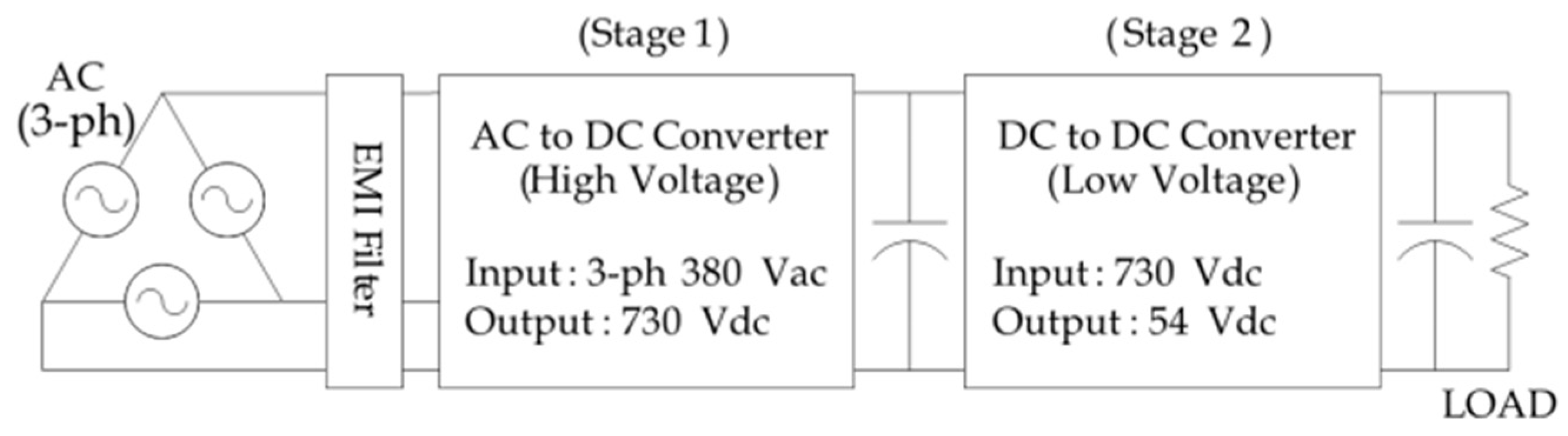
Generally, a power-supply system for communications requires a high power factor and wide bandwidth response characteristics. For this reason, the majority of power-supply systems for communications have a two-stage configuration, as shown in Figure 1, including an AC/DC rectifier with a power-factor correction (PFC) function and a DC/DC converter with insulation between the primary and secondary circuits. The high-capacity power-supply system using a large input voltage usually applies three-phase power. The PFC circuit uses a boost-type two-level pulse-width modulation rectifier or three-level Vienna rectifier. The insulation-type DC/DC converter is typically designed by using a soft-switching topology to consider efficiency and size.
Because a rectifier using three-phase power as an input has a large DC link voltage, a DC/DC converter needs to use a power-switching element with a large breakdown voltage and low conduction loss, like an insulated gate bipolar mode transistor (IGBT). However, as IGBT undergoes a drastic increase in switching loss due to the tail current, it is not appropriate for fast switching. Accordingly, a low switching frequency is generally used to minimize the loss of the switching element, which increases the volumes and capacities of the inductor and capacitor. Furthermore, a high output-to-input voltage ratio causes a large transformer loss. Various studies have attempted to minimize the loss of the transformer by constructing a high-capacity converter. To solve this issue, a Vienna rectifier was used to dissolve a voltage imbalance by controlling the voltage of the center point of the link capacitor in the AC/DC rectifier on the basis of a three-level space-voltage vector [1], and the series-connected DC/DC converter used a metal–oxide–semiconductor field-effect transistor (MOSFET) element for soft switching [
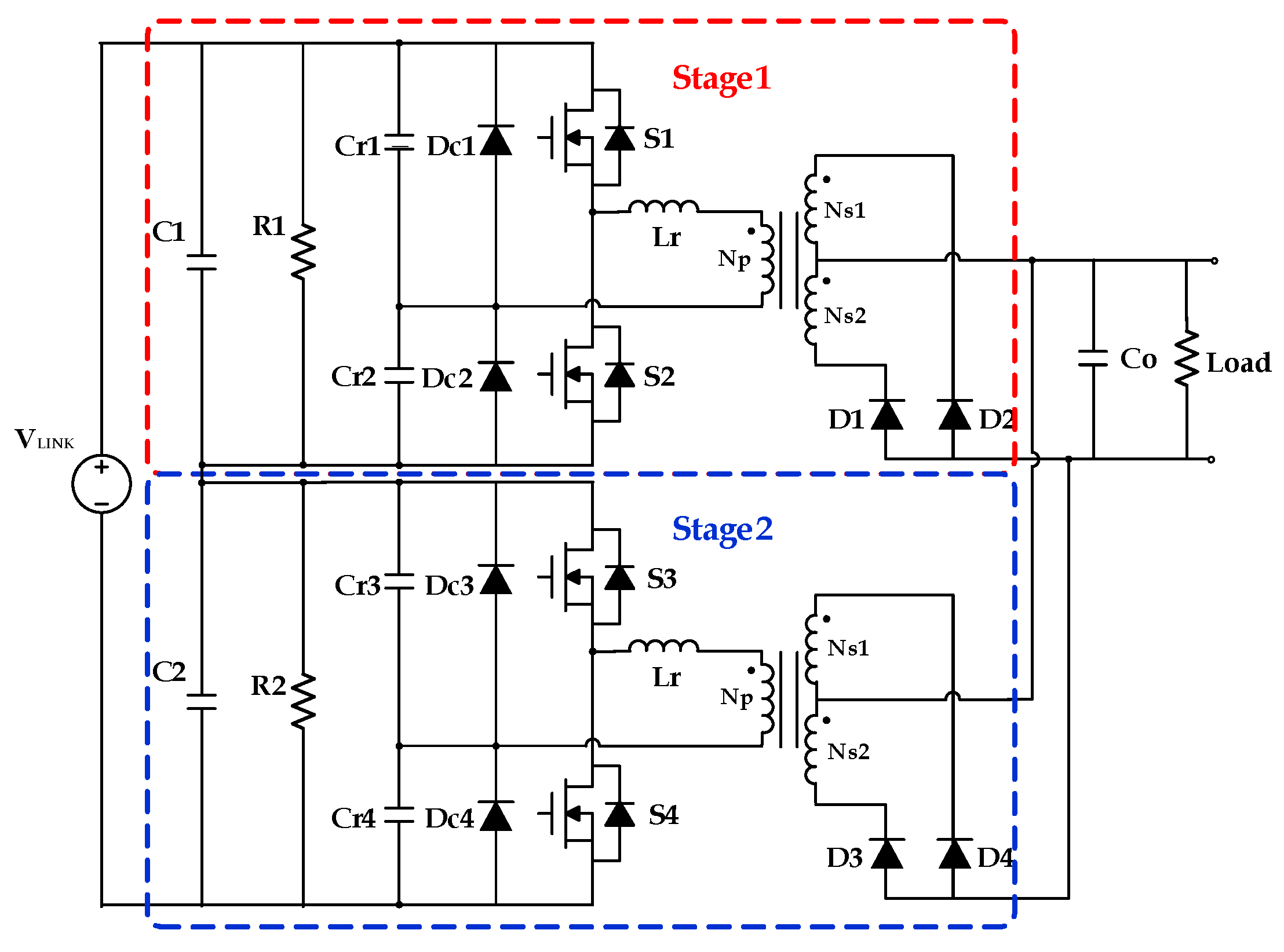
2] so called input series and output parallel (ISOP), which divides a large DC link voltage into smaller voltages and has a low withstand voltage and good switching performance as shown in Figure 2.
In this way, the efficiency was improved and the volume was minimized. Moreover, to solve the problem of miniaturization, converters with the same module were connected by input serial and output parallel (ISOP) topology [3,4,5,6,7,8,9]. However, this method may cause a problem of power imbalance between equivalent modules connected by ISOP. Among representative methods of solving this problem, Reference [3] permits a certain imbalance between ISOP converter modules by permitting an imbalance of DC link voltage which called the auto-balancing method in that patent, and other methods divide the currents by independently controlling DC/DC converters [4,5,6] or utilizing a coupling inductor [7]. Unfortunately, these methods cannot perfectly solve the fundamental problem of power imbalance, which is attributable to complex circuits or control and the difference among elements. Another method used a single multiple-input transformer to solve the problem of power imbalance [8]. However, this method cannot also solve the problem of increasing volume due to the heat concentrated in the transformer. This study proposes a new solution to the power imbalance of the DC/DC converter, which applies a new topology for the magnetic coupling of the transformer. Section 2 analyzes the cause of the power imbalance of LLC resonant DC/DC converter with an ISOP auto-balancing configuration. The power imbalance of each converter is caused by passive elements, active elements, and the control signal. Among these factors, the difference in the magnetic elements is most influential. 
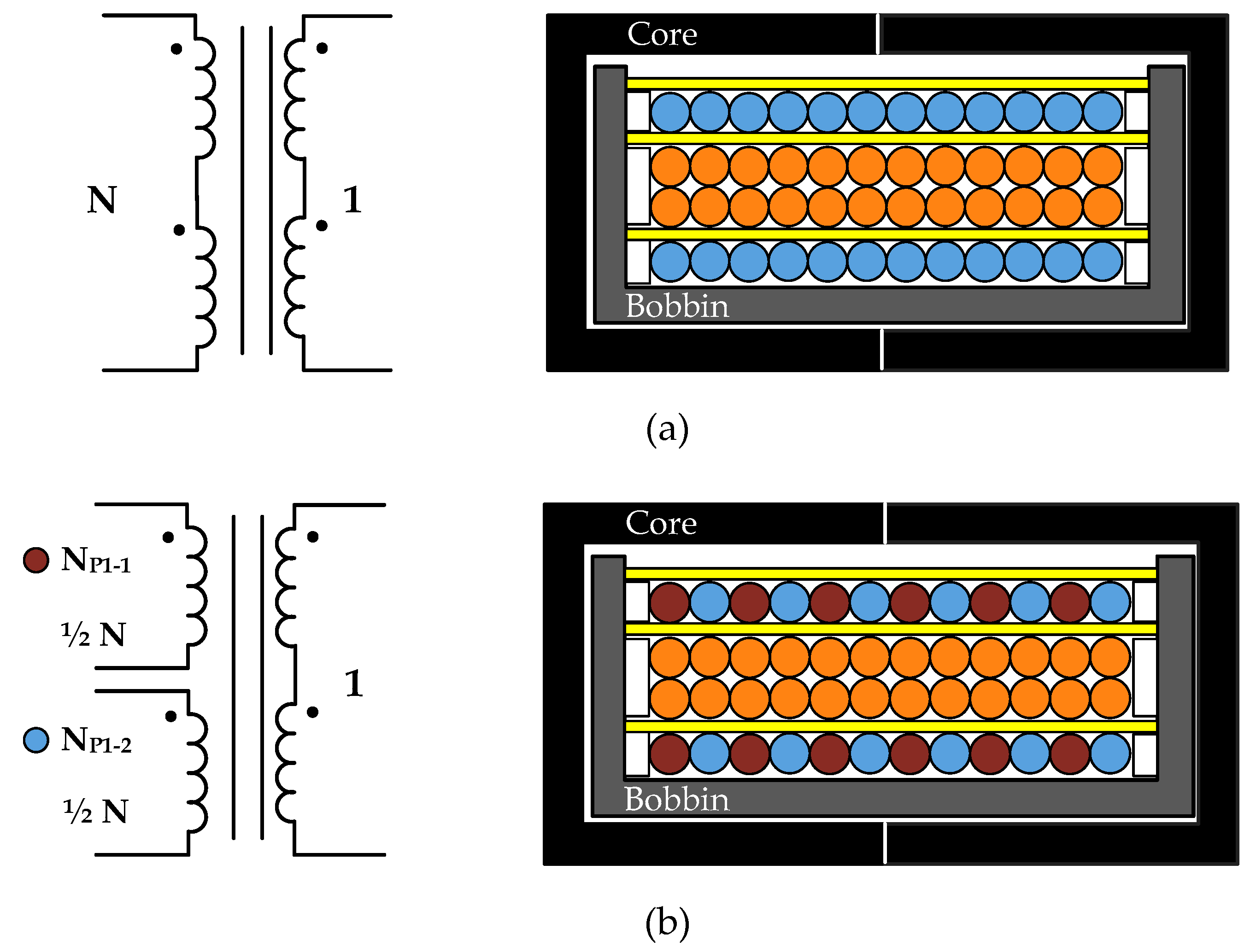
Section 3 proposes a new topology for LLC resonant DC/DC converters, which uses a coupled shunt inductor and multiple-input transformers that share magnetic coupling in order to solve the problems of miniaturization and power imbalance in DC/DC converters. Section 4 presents the proposed winding method for a multi-input transformer. Section 5 applies the design parameters of the proposed LLC resonant DC/DC converter using a coupled shunt inductor and multiple-input transformers sharing magnetic coupling to a PSIM simulation tool to comparatively analyze the power imbalances. Section 6 designs the prototype power-supply system by applying the proposed topology and verifies the effectiveness of the proposed method through simulation and experiment.

2. Power Imbalance Problem of ISOP Auto-balancing Converter

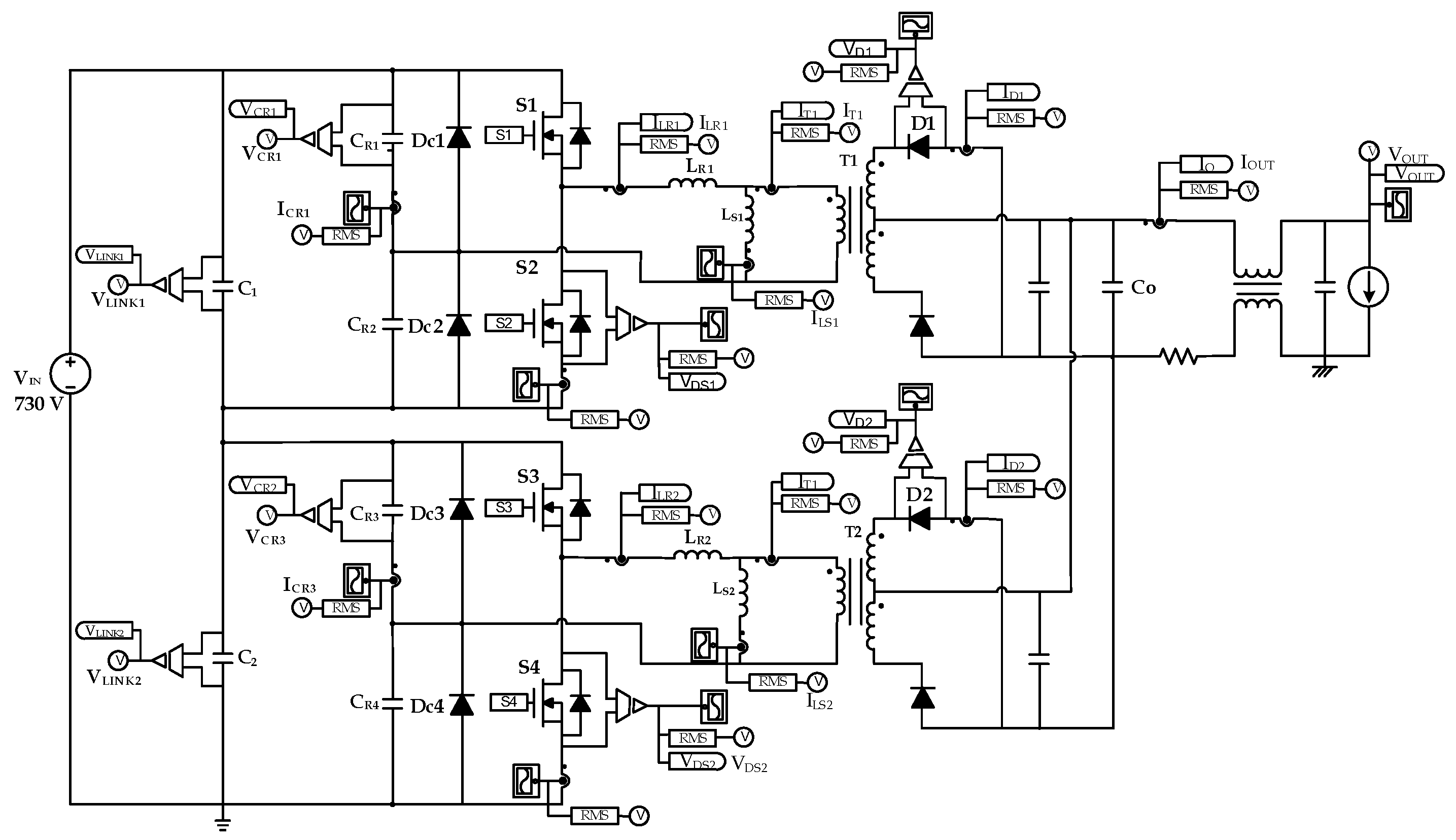
One of the most representative methods for solving the problem of DC/DC converters with a large output-to-input voltage ratio is configuring two DC/DC converters with the ISOP auto-balancing configuration shown in Figure 2. In this figure, resonant capacitors Cr1 and Cr2, and Cr3 and Cr4 are separated, which was reported in References [10,11,12,13]. By this configuration, the voltage of the resonant capacitors with anti-parallel diodes can be limited by the diode clamping feature under the over load condition. As LLC resonant DC/DC converter 1 of stage 1, which is connected in series, and LLC resonant DC/DC converter 2 of stage 2 can be easily controlled by the same control circuit and pulse signal, this method is widely used. The auto-balancing method uses two series-connected DC link capacitors C1 and C2 and two series-connected DC/DC converters to divide a large voltage into smaller ones. The secondary circuit is connected in parallel, while the primary circuit of the DC/DC converter is connected in series. If the load current increases at the DC/DC converter 1 due to power imbalance, the voltage of C1 decreases and that of C2 increases. This reduced voltage of C1 can reduce the load current of the DC/DC converter 1. On the other hand, as the load current increases at DC/DC converter 2 due to power imbalance, the voltage of C2 decreases and this reduced voltage of C2 can reduce the load current of the DC/DC converter 2. In this circular structure, the voltages of C1 and C2 are automatically adjusted according to the power imbalance condition. The power imbalance of each DC/DC converter is attributable to deviations related to passive and active elements and control signals. However, this auto-balancing method cannot solve this imbalance of the DC link voltage, perfectly. Power imbalance results in various problems. Firstly, higher DC link voltage can be generated, causing a high withstand voltage of the link capacitors, thereby selecting a large capacitor voltage rating. When power balancing, the DC link voltage can be exactly divided by 1/2Vdc for every series-connected capacitor C1 and C2, but if power imbalance occurs, a voltage higher than 1/2Vdc is applied to either C1 or C2. Secondly, the DC/DC converter where the high voltage is applied needs to use a switching device having a high voltage and a large capacity because of high power. Thirdly, converters with biased power lead to designs to ensure margins for heat dissipation as losses also increase. This problem of power imbalance increases the overall volume and cost. Another problem of the auto-balancing method can occur when a three-level Vienna rectifier is used as the PFC rectifier. Three-level Vienna rectifier can control the DC link capacitor voltage unbalance [14]. When the DC link voltage unbalance can be controlled, auto-balancing cannot be actively operated.
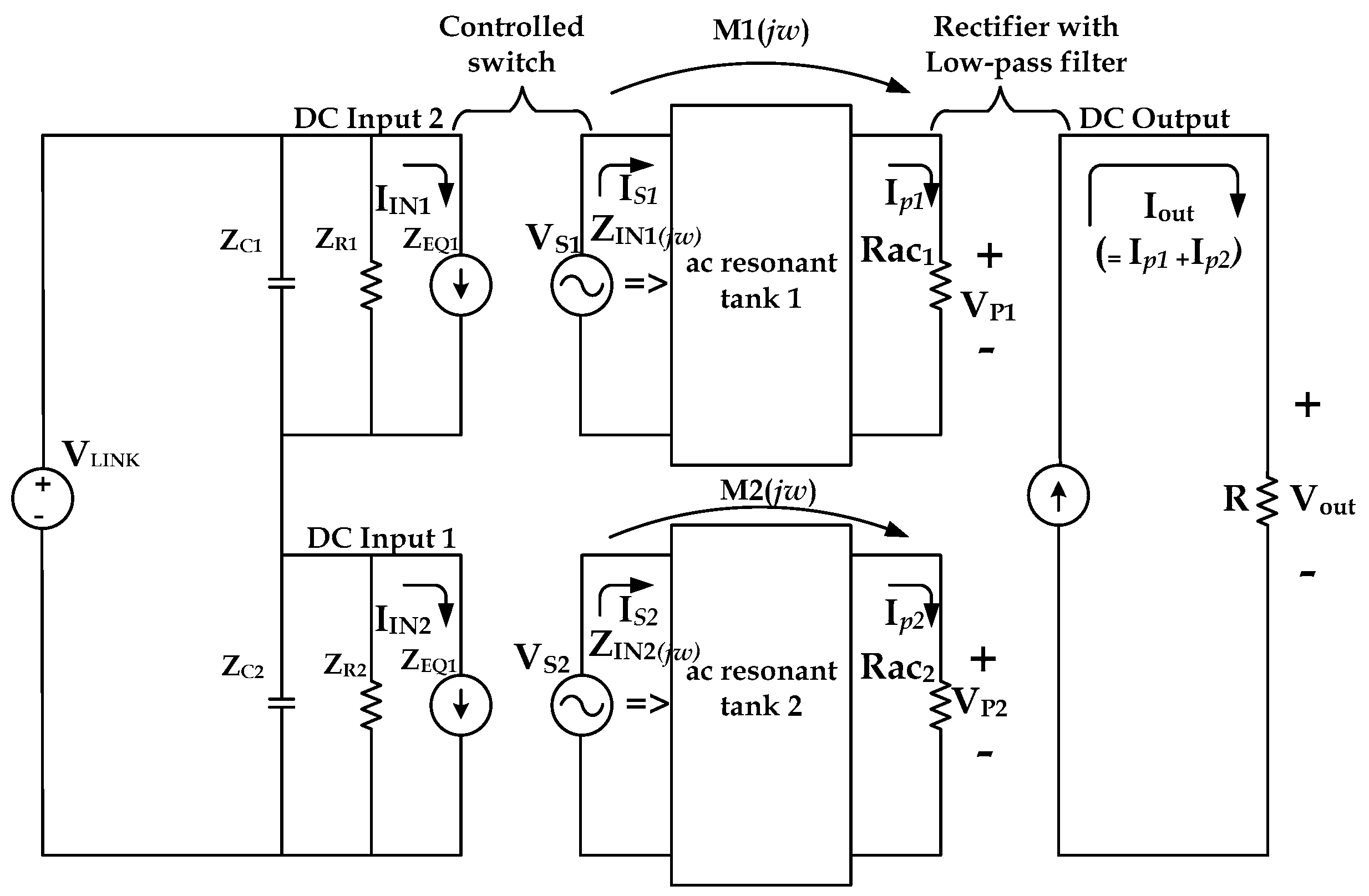
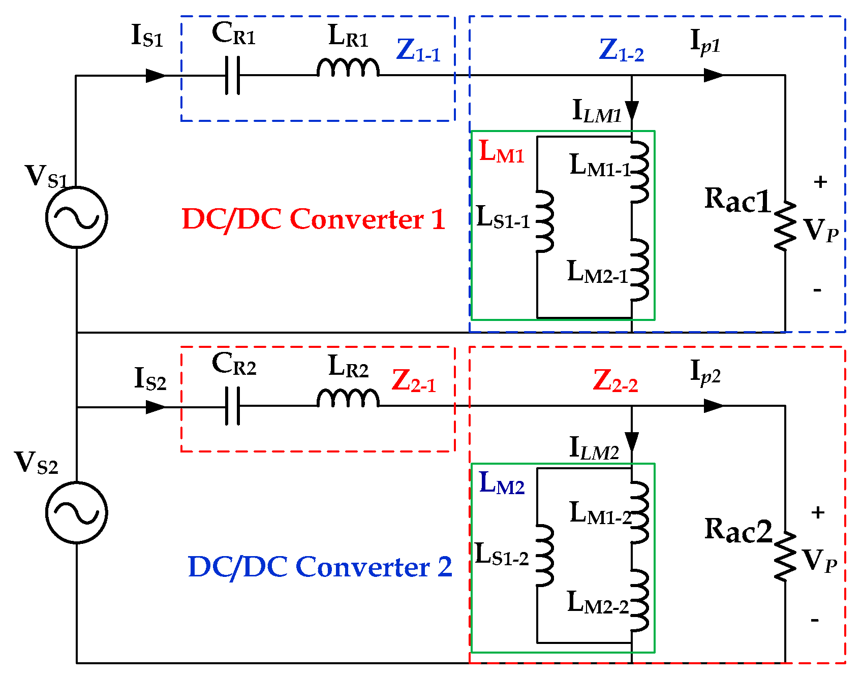
The power imbalance is mainly caused by a leakage inductor deviation, which determines the input impedance of a resonant tank, and a magnetizing inductor deviation of the transformer delivering power. The AL-value of the ferrite core, which determines the leakage and magnetizing inductances, has a maximum deviation of ±25%. For this reason, using two different shunt inductors and a transformer leads to the factor that causes the largest power deviation. An equivalent circuit can be expressed as in Figure 3 [15,16]. In this figure, the circuit of the auto-balancing LLC resonant converter includes DC link capacitors (C1, C2) to divide a large input voltage and balance resistances (R1, R2) to prevent voltage imbalance under no load condition; LLC resonant networks (AC resonant tank) that are independent from each other and a low-pass filter of the parallel structure sharing output can be seen in Figure 2.
In Figure 3, the input impedance Z E Q 1 of DC/DC converter 1 can be defined as follows.
Z E Q = V l i n k 2 I i n
where V l i n k is the DC link voltage and I i n is the input current of DC/DC converter 1 and represented as Equation (2),
I i n = I s .
In this equation, I s represents the primary side current of the DC/DC converter, and the primary side voltage and current are in phase. On the simplified impedance model of the DC link side shown in Figure 3, the condition for power balance can be expressed by Equation (3) below.
Z C 1 | | Z R 1 | | Z E Q 1 = Z C 2 | | Z R 2 | | Z E Q 2 ,
where ZC1 and ZC2 denote the impedances of DC link capacitors; ZR1 and ZR2 are the impedances for preventing imbalance; and ZEQ1 and ZEQ2 are the input impedances of the resonant tanks. In order to obtain the power balance, DC/DC converters 1 and 2 should have the same parallel impedance. However, the power imbalance occurs due to an impedance deviation among these impedance elements. In this article, it is assumed that the DC link capacitance values are exactly the same. Generally, the electrolytic capacitor used as a DC link capacitor has small parameter deviations compared to magnet elements. Besides, if a three-level Vienna rectifier is used as the PFC, the DC link capacitor unbalance can be controlled. So, there is no need to consider the DC link capacitance unbalance problem for the case of using a three-level Vienna rectifier. On the other hand, the impedance (ZR1, ZR2) of the resistances for preventing imbalance are much larger than the input impedances (ZEQ1, ZEQ2) of the resonant tank; they have little influence on power imbalance as shown in Equation (4).
Z R 1 Z E Q 1 = Z R 2 Z E Q 2 .    
As the resistance for preventing imbalance ranges from dozens to hundreds of kilo-ohms depending on voltage, the impedance (ZR) of resistance is also much larger than the equivalent impedance (ZEQ) of the LLC resonant converter.
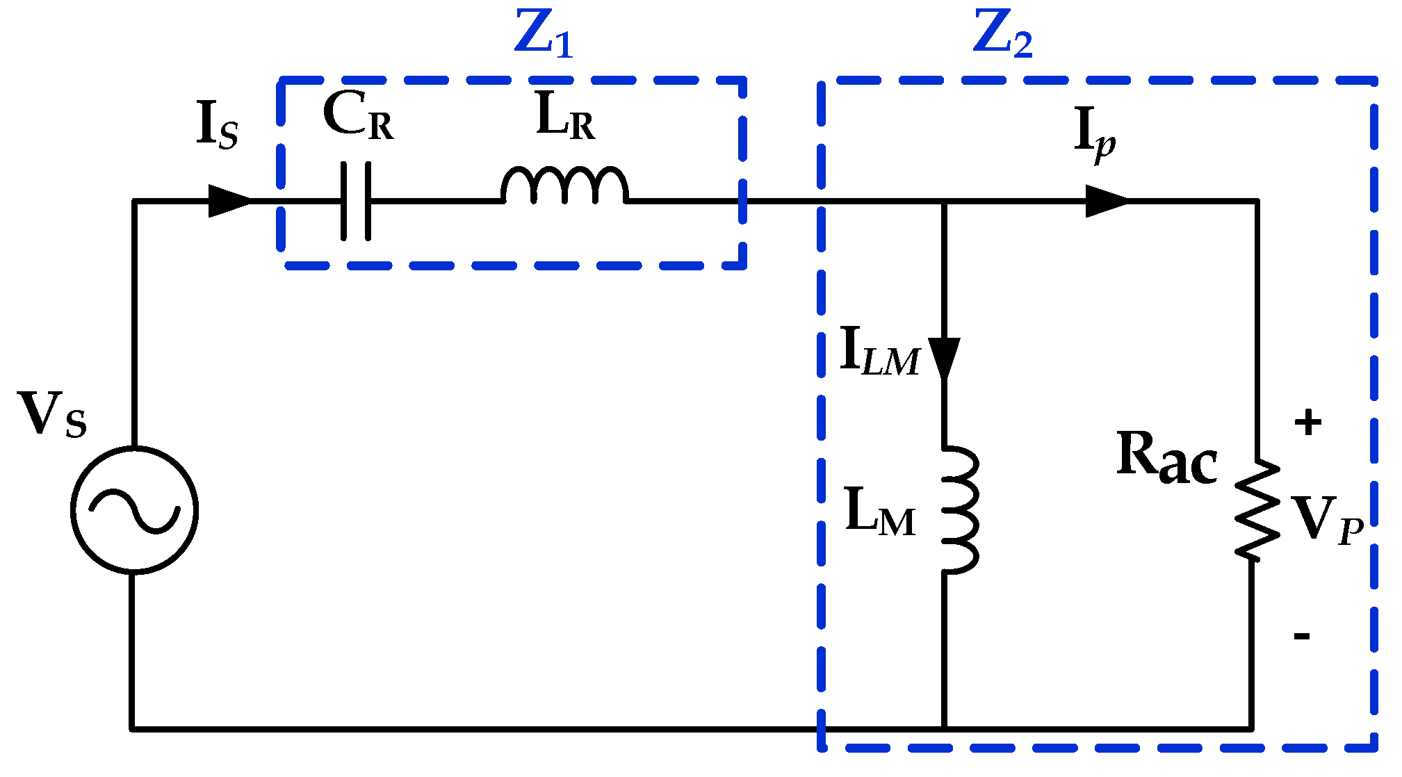
Figure 4 shows the equivalent circuit of the AC resonant tank. If the series impedance of the resonant capacitor (CR) and the resonant inductance (LR) is Z1 and the parallel impedance of the magnetizing inductance (LM) and the AC impedance (Rac) is Z2, the input impedance (ZIN) of the resonant tank can be expressed by the following equation.
Z I N = V s I s = Z 1 + Z 2
where V s represents the AC source voltage of LLC converter and is made by half of the DC link voltage V l i n k 2 ; Z1 and Z2 can be expressed as following:
Z 1 = j ω s L R j 1 ω s C R ,     Z 2 = j ω s L M / / R a c = j ω s R a c L M R a c + j ω s L M .
From Equations (5) and (6), the input impedance of the LLC converter can be expressed as
Z I N = j ω 0 ( ω s ω 0 ) L R j 1 ω 0 ( ω s ω 0 ) C R + j R a c L M R a c ( 1 ω s ) + j ω s L M = j ω n Z O j Z O ω n + j R a c K L R a c Z O ( 1 ω n ) + j K L = Z O ( j ω n j 1 ω n + j ω n K L 1 + j ω n K L Q ) ,
where ω S is the switching frequency of the LLC converter, ω O is the resonant frequency of the resonant inductance (LR) and the resonant capacitance (CR), and Zo is the characteristic impedance of resonant inductance (LR) and resonant capacitance (CR). ω n is a normalized angular frequency indicating the ratio between the switching frequency ( ω s ) and the resonant switching frequency ( ω 0 ), Rac is a load resistance, and KL is the constant indicating the ratio between the resonant inductance (LR) and the magnetizing inductance (LM), as expressed in Equation (8) below.
      K L = L M L R ,   R a c = 8 N 2 π 2 R L ,   ω o = 1 L R C R
Z O = L R C R ,     Q = Z O R a c ,     ω n = ω S ω O = f S f O
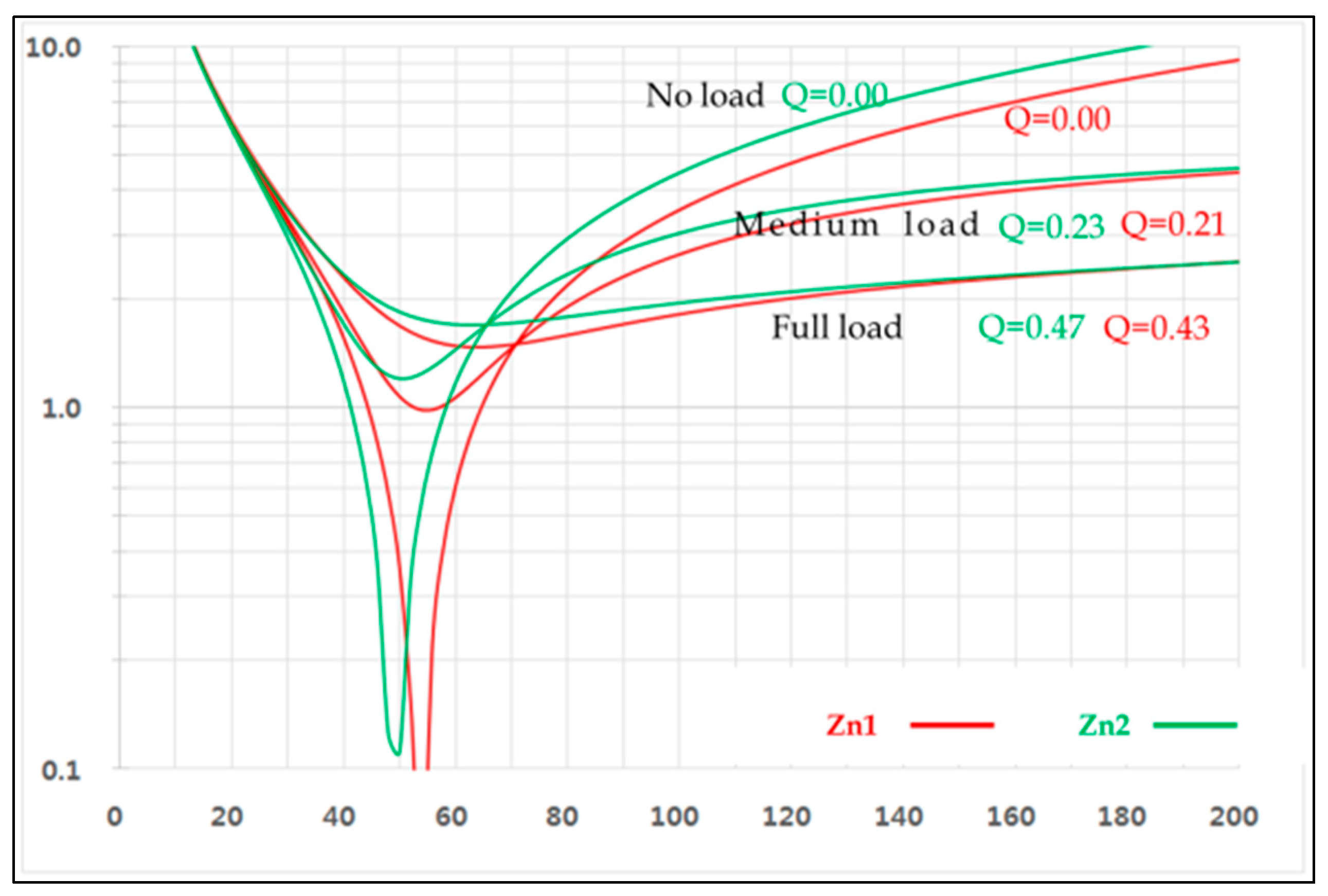
From the input impedance (Z
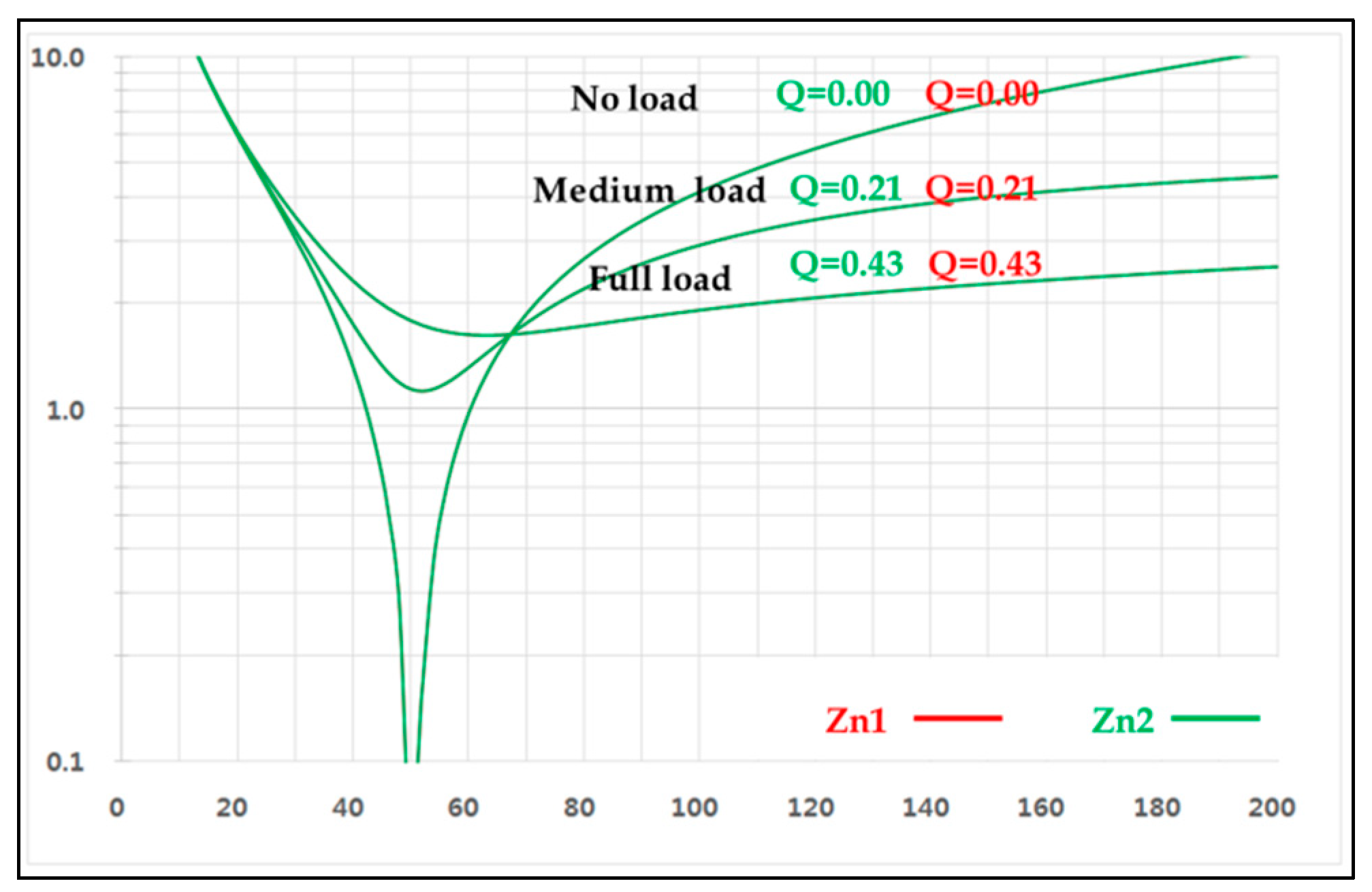
IN) of Equation (7), the normalized impedance (Zn) according to frequency can be obtained as shown in following equation.
Z n = Z I N Z O = j ω n j 1 ω n + j ω n K L 1 + j ω n K L Q   = j ω n j 1 ω n + j ω n K L ( 1 j ω n K L Q ) ( 1 + j ω n K L Q ) ( 1 j ω n K L Q )
| Z n | = | Z I N Z O | = ( ω n 2 K L 2 Q 1 + ω n 2 K L 2 Q 2 ) 2 + ( ω n 1 ω n + ω n K L 1 + ω n 2 K L 2 Q 2 ) 2
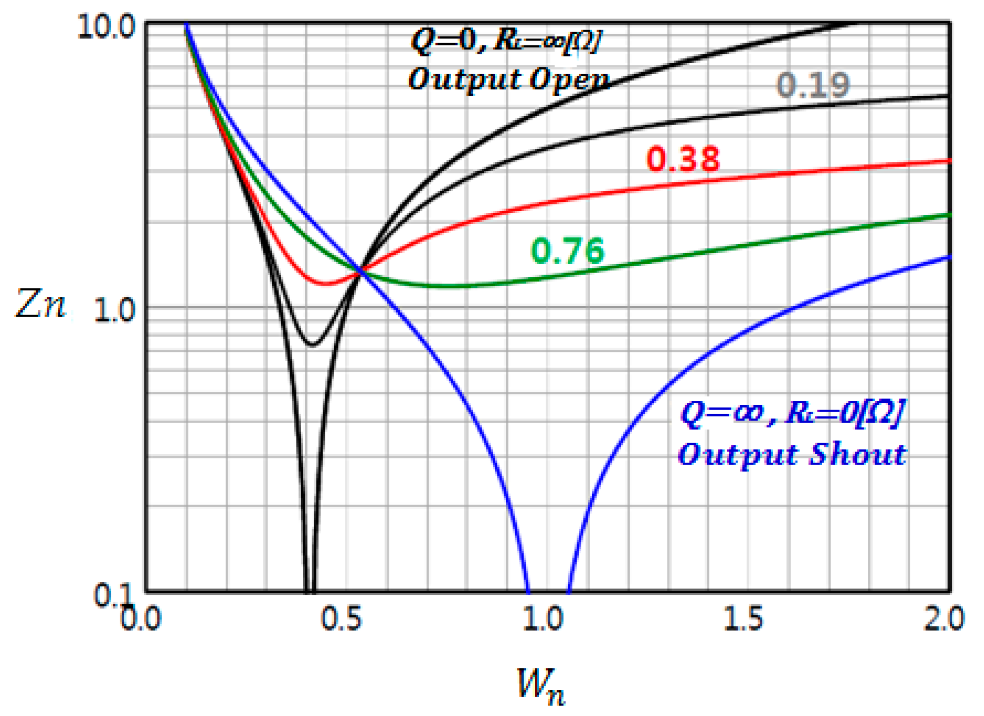
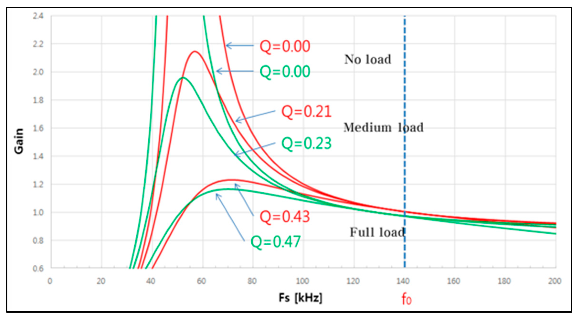
The input impedance characteristics at each switching frequency of the LLC resonant converter can be obtained by varying the switching frequency in Equation (9) under the condition of Q = ∞ (Rac = 0), as described in following Equation (10). The characteristic graph is V-shaped and depicted in blue. In the case of ω n = 1 , the input impedance becomes 0, and when ω n = 0 and ω n = , Z n = .
ω n = 1 ,   | Z n | = | Z I N Z O | = ( 1 2 × K L 2 × 1 + 1 2 × K L 2 × 2 ) 2 + ( 1 1 1 + 1 × K L 1 + 1 2 × K L 2 × 2 ) 2 =   0      
ω n = 1 1 + K L ,   | Z n | = | Z I N Z O | = ( ω n 2 × K L 2 × 1 + ω n 2 × K L 2 × 2 ) 2 + ( ω n 1 ω n + ω n K L 1 + ω n 2 × K L 2 × 2 ) 2        = 0 + ( ω n 1 ω n + 0 ) 2 = ω n 2 1 ω n = | ( K L ) 1 + K L | = K L 1 + K L
ω n = 0 ,   | Z n | = | Z I N Z O | = ( 0 × K L 2 Q 1 + 0 × K L 2 Q 2 ) 2 + ( 0 1 0 + 0 × K L 1 + 0 × K L 2 Q 2 ) 2 =
ω n = ,   | Z n | = | Z I N Z O | = ( × K L 2 Q 1 + × K L 2 Q 2 ) 2 + ( 1 + × K L 1 + × K L 2 Q 2 ) 2 =
In addition, Equation (11) can be obtained by varying the switching frequency in Equation (9) under the condition of Q = 0 (Rac = ∞). The characteristic graph is V-shaped and depicted in black, where ω n = 1 results in the input impedance of KL and, when both ω n and ω n are 0, the result is Z n = .
ω n = 1 ,   | Z n | = | Z I N Z O | = ( 1 2 × K L 2 × 0 1 + 1 2 × K L 2 × 0 2 ) 2 + ( 1 1 1 + 1 × K L 1 + 1 2 × K L 2 × 0 2 ) 2 = K L
ω n = 1 1 + K L ,   | Z n | = | Z I N Z O | = ( ω n 2 × K L 2 × 0 1 + ω n 2 × K L 2 × 0 2 ) 2 + ( ω n 1 ω n + ω n K L 1 + ω n 2 × K L 2 × 0 2 ) 2            = ω n 1 ω n + ω n K L = ω n 2 1 ω n + ω n K L = | ( K L ) 1 + K L + ( K L ) 1 + K L | = 0
ω n = 0 ,   | Z n | = | Z I N Z O | = ( 0 × K L 2 Q 1 + 0 × K L 2 Q 2 ) 2 + ( 0 1 0 + 0 × K L 1 + 0 × K L 2 Q 2 ) 2 =
ω n = ,   | Z n | = | Z I N Z O | = ( × K L 2 Q 1 + × K L 2 Q 2 ) 2 + ( 1 + × K L 1 + × K L 2 Q 2 ) 2 =
From the above two conditions, the input impedance characteristic graph of the LLC converter according to frequency and Q can be expressed as in Figure 5.
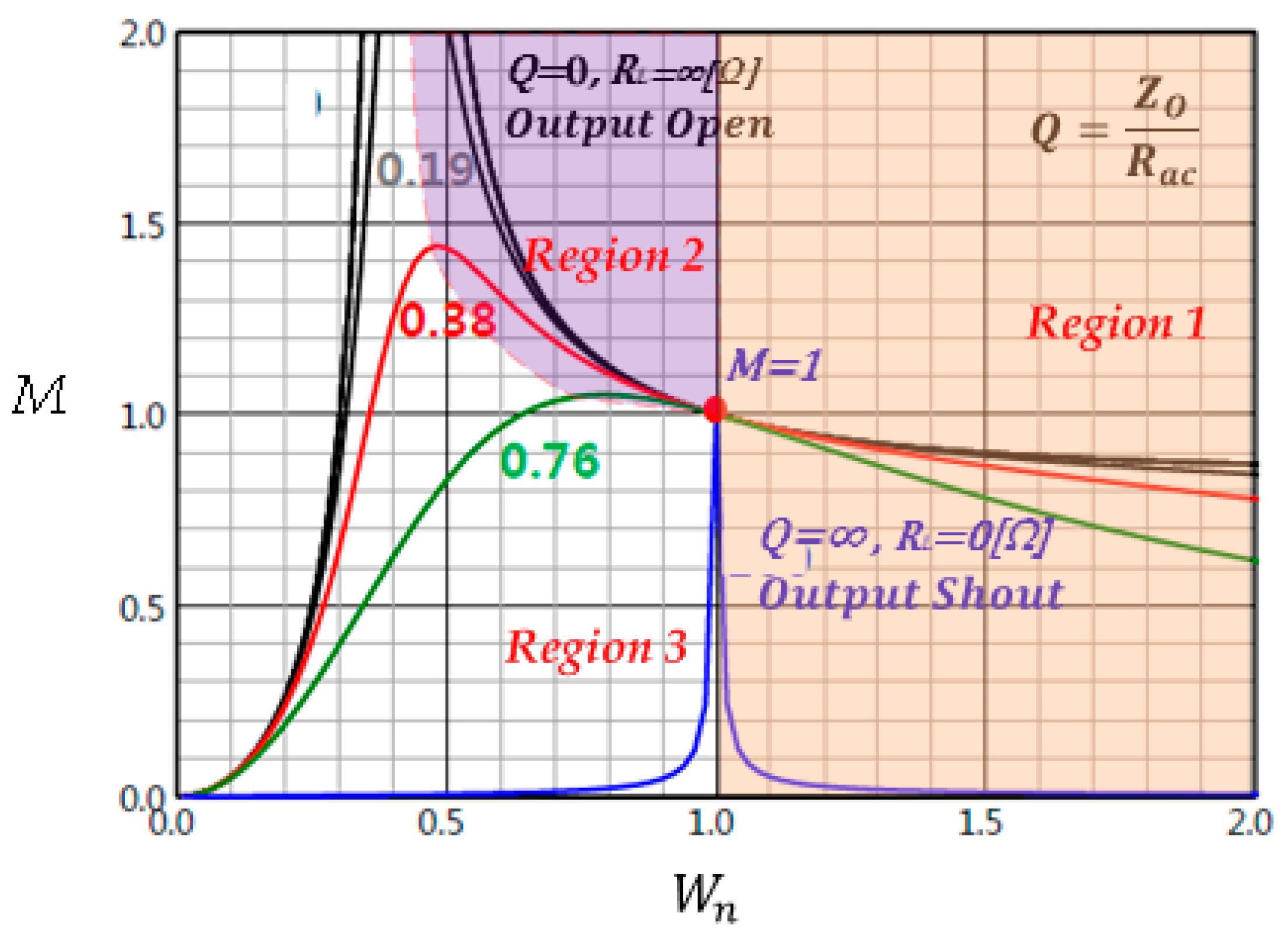
On the other hand, the input–output voltage gain of the LLC resonant converter can be expressed by Equation (12).
M = 2 n V O V I N = ω n K L K L 2 ( 1 ω n 2 ) Q 2 + ω n 2 ( K L + 1 + 1 ω n 2 ) 2 ,
where V o denotes the output voltage and n is the number of turns of the transformer. From Equation (12), the input–output voltage gain needs to be changed to change the output voltage, when the input voltage is fixed. When the circuit of the LLC converter is designed, every value is fixed including winding ratio (n), ratio between resonant inductance (LR) and magnetizing inductance (LM), resonant frequency ( ω 0 ), and characteristic impedance (Zo). As the quality factor (Q) at a specific load resistance (Rac) is also fixed, the switching frequency ( ω s 
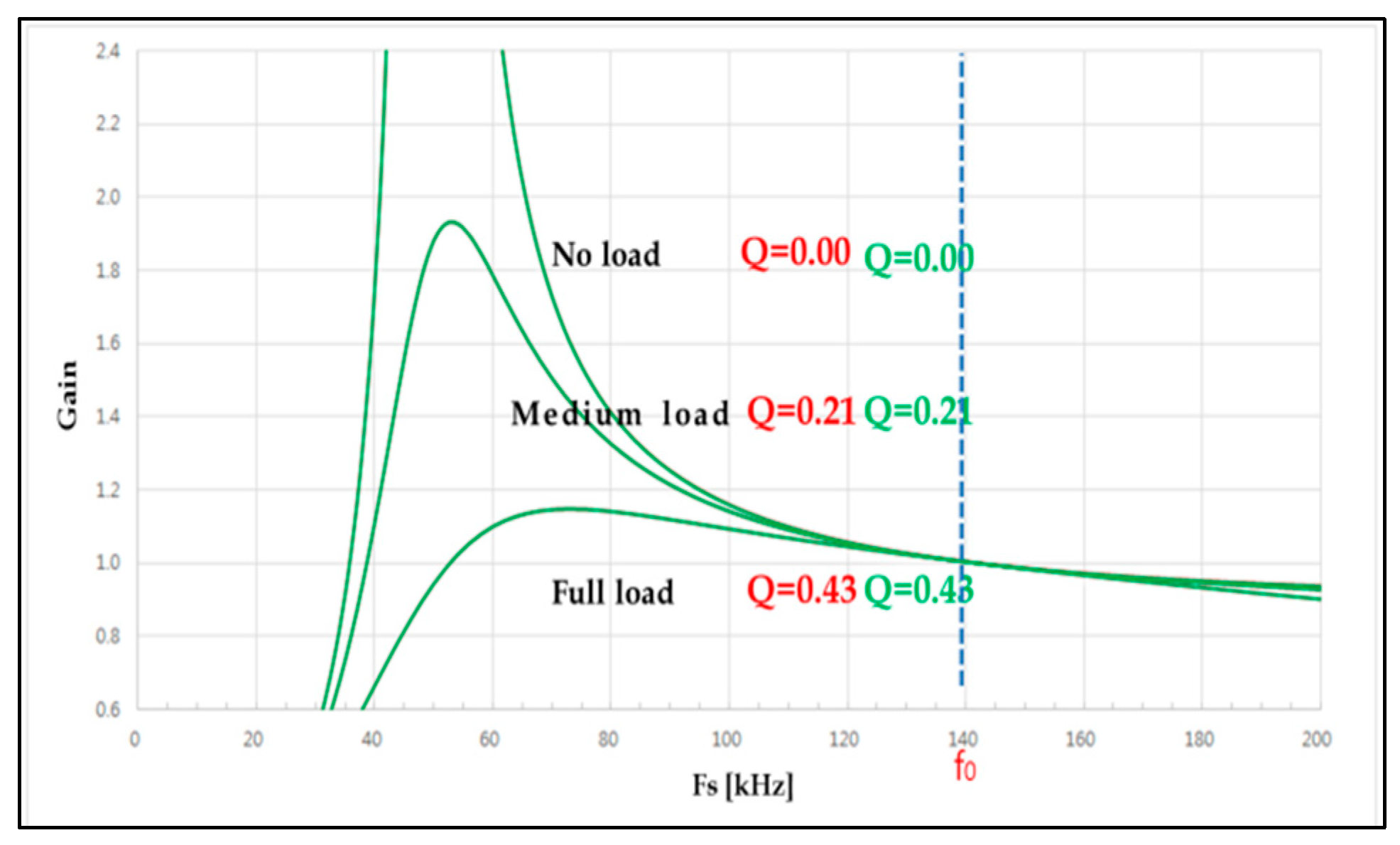
) needs to be changed in order to modify the input–output voltage gain (M). As shown in Figure 6, the characteristic graph of the input–output voltage gains according to the frequency variation at a specific load resistance (Rac) can be expressed through Excel. The characteristic graph of Figure 6 shows that the value of Q is inversely proportional to the gain. The switching frequency and the resonant frequency meet at the point of M = 1. Both frequencies pass this point under every load.
The input impedance and frequency characteristic graph (Figure 5), which was derived from Equations (9) and (11), and the input–output voltage gain and frequency characteristic graph (Figure 6) show that the voltage gain (M) characteristic and the input impedance (ZIN) characteristic change according to variation of the quality factor (Q). The independent transformers used for two auto-balancing LLC resonant DC/DC converters generate a deviation between magnetizing inductance (LM) and leakage inductance by winding method and ferrite-core characteristic. The deviation between magnetizing inductance (LM) and leakage inductance in a transformer changes the constant KL, that is the ratio between resonant inductance (LR) and magnetizing inductance (LM), and thus, not only does the resonant frequency of the AC resonant tank change, but also the quality factor (Q) is affected, which results in a difference in the input characteristic impedance according to the frequency characteristic. In other words, when independent transformers are used, the deviation between magnetizing inductance (LM) and leakage inductance becomes the primary cause of power imbalance, because it generates a difference between the input–output voltage gain characteristic and the input impedance (ZIN).

3. Proposed LLC Resonant DC/DC Converter Using Coupled Shunt Inductor and Multiple Input Transformers with Magnetic Coupling Being Shared

3.1. Proposed Circuit

To solve the problem of the ISOP converter, this study proposes a method of minimizing the occurrence of power imbalance due to impedance deviation by using a coupled shunt inductor and two multiple input transformers, which makes DC/DC converters share magnetic coupling. The proposed new topology is illustrated in Figure 7. The equivalent circuit of the AC resonant tank is shown in Figure 8.
The conventional LLC resonant converter is designed to have a small magnetizing inductance (LM) to make the gain curve have a steep slope, however, this increases the circulating current. In this manner, its wide input range and load variation can be covered. To decrease LM, a transformer gap is reflected in the design. Accordingly, the coupling factor of transformers decreases, and the heat of transformers increase due to the circulating current and load current. The typical solution to this problem is adding and using a shunt inductor, which functions as a separate LM [11]. However, such a shunt inductor can hardly achieve a uniform LM because of the characteristics variation of transformer cores. This study used a coupled shunt inductor and two multiple input transformers to make DC/DC converters share magnetic coupling with each other and thus minimize the power imbalance caused by an impedance deviation. In the DC/DC converter topology proposed by this study, the coupling shut inductance (LS) wound around a single core and the magnetizing inductance (LM) of transformers sharing the winding are magnetically shared with each other. For this reason, even if the deviation of magnetizing inductance between Transformer 1 (Tr1) and Transformer 2 (Tr2) is +10% or −10%, no deviation between LS and LM occurs and thus the input impedances (ZIN1, ZIN2) are equal. As shown in Figure 8, LS1-1 and LS1-2 of the shunt inductor (LS) are coupled, and the primary winding (NP1-1) and NP1-2 of Tr1 in DC/DC converter 1 and NP2-1 and NP2-2 of Tr2 in DC/DC converter 2 are magnetically coupled. NP1-1 of Tr1 and NP2-1 of Tr2 are connected in series and then connected in parallel to LS1-1. NP1-2 of Tr1 and NP2-2 of Tr2 are connected in series and then connected to LS1-2 in parallel. Accordingly, converter 1 and 2 are operated by being magnetically shared with each other. In other words, such magnetic coupling makes magnetizing inductances (LM1, LM2) equal, and thus, a type of parallel operation of 2 DC/DC converters comprising the same components is realized. In this manner, the condition for power balance, as expressed by Formula (1) above, is satisfied.
The auto-balancing converter generates a deviation between the magnetizing inductance (LM) and the parasite inductance (LR) due to independent shunt inductor and transformers. On the other hand, the proposed converter using a coupled shunt inductor and multiple input transformers magnetically shares the magnetizing inductance (LM) and the parasite inductance (LR), which makes the constant KL, that is, the ratio between the resonant inductance (LR) and the magnetizing inductance (LM) equal to the quality factor (Q). Thus, because the input–output voltage gain characteristic and the input impedance become the same according to frequency variation in AC resonant tank 1 and 2, the power imbalance due to magnetic elements like shunt inductor and transformers can be solved.

3.2. Proposed Winding Method of Multi-Input Transformer

In a typical circuit as shown in Figure 2, an independent transformer is used and the winding method is shown in Figure 9a. Even if the winding is precise when using independent transformers, the inherent characteristic deviation of the core cannot be solved and the power imbalance of the series-connected DC/DC converters 1 and 2 appears. The winding method of the transformer for the proposed ISOP circuit is shown in Figure 9b in which Tr1 and Tr2 of the DC/DC converters 1 and 2 share a winding through magnetic coupling. The deviation of the ferrite core can be overcome through the magnetic sharing of the multi-input transformer. NP1-1 of Tr1 and NP2-1 of Tr2 are connected in series, NP1-2 of Tr1 and NP2-2 of Tr2 are connected in series, and two transformers are connected magnetically so that there is no deviation and the inductance is the same. However, the multiple input transformers winding scheme must be precisely wound. The leakage inductance error occurs due to the physical position difference between the two primary side windings, and this leakage inductance participates in the resonance to cause an error in the resonance frequency, which causes a power imbalance. Therefore, by introducing a winding method that minimizes the difference in leakage inductance, it is possible to reduce the stress of the input terminal power device and improve the efficiency by eliminating the power unbalance. The multi-input transformer winding method uses a sandwich winding method in which a secondary winding is connected between the primary windings, and winding the NP1-1 and NP1-2 windings at the same time greatly reduces the physical position difference between the primary windings to increase the leakage inductance. The impedance difference can be minimized.

4. Simulation of the LLC Resonant DC/DC Converter Using Coupled Shunt Inductor and Multiple Input Transformers Sharing Magnetic Coupling

An auto-balancing converter circuit, the proposed topology of a coupled shunt inductor and two multiple input transformers sharing magnetic coupling were applied to an LLC resonant converter with the primary-series and secondary-parallel connection to conduct a simulation by using Excel and PSIM. The prototype product had a deviation between the resonant capacitor (CR) and resonant inductor (LR) due to errors of components. However, the simulation assumed that there was no such deviation between the capacitor (CR) and the resonant inductor (LR). The deviation of magnetizing inductance (LM) between the shunt inductor and the transformers, which was the largest deviation, was set to ±10%.

4.1. Simulation of Auto-balancing Converter Circuit

Figure 10 shows the simulation circuit for the auto-balancing converter, which was obtained by PSIM. Independent shunt inductor and transformers were used, and the magnetizing inductance (LM1) of Converter 1 and that (LM2) of Converter 2 were set to 32.4 µH and 39.6 µH, respectively, and thus, the deviation of magnetizing inductance (LM) was set to ±10% for simulation.
Figure 11 presents the PSIM simulation result for the auto-balancing converter. Owing to the deviation of magnetizing inductance (LM) between the independent shunt inductor and transformer, the voltage applied to the link capacitor was divided into 345 V (VLINK1) and 385 V (VLINK2). Accordingly, the voltage imbalance of 40 VDC occurred. Besides, the resonant currents of the resonant tanks were 14.1 A (LR1) and 15.4 A (LR2), which corresponded to 1.3 A current imbalance. The currents at the secondary rectifier diodes were 34.3 A (ID1) and 39.7 A (ID2), and thus the current deviation was 5.4 A. A current imbalance of 1.2A occurred at IT1 = 14.8 A, IT2 = 13.6 A, and a current difference of 1.6 A at ILS1 = 5.7 A and ILS2 = 7.3 A was generated in the shunt inductor. The voltage across VCR1 = 220 V and VCR2 = 198 V across the resonant capacitor caused an imbalance of 22 V. The currents flowing through the resonant capacitor ICR1 = 8.23 A and ICR2 = 9.23 A caused 1 A current imbalance.
The graphs of Figure 12 and Figure 13 which were obtained from an Excel-based simulation show the input-output voltage gains and impedance characteristics of the auto-balancing converter according to frequency variations.
As shown in Figure 12 and Figure 13, the deviation of magnetizing inductance (LM) between the shunt inductor and the transformer caused a deviation between the quality factor (Q) and the constant KL, that is, the ratio between the resonant inductance (LR) and the magnetic inductance (LM). Thus, it turned out that the power imbalance occurred because the input–output voltage gain (M) of DC/DC converter 1 and 2 was different from the input impedance characteristic (Zn) at the same frequency. The red characteristic curve shows the quality factor (Q) and input impedance (Zn) of DC/DC converter 1, and the green curve displays those of DC/DC converter 2. These results were obtained under maximum, medium and no-load conditions. Table 1 presents the PSIM simulation result obtained by using a independent shunt inductor and transformer for the auto-balancing converter. Deviations of input impedance, input voltage and output power are shown. As is clear from Table 1, the largest deviation occurred when the output load was smallest, and the deviation decreased when the switching frequency was equal to the resonant frequency. Besides, as the load increased, the deviation of the input voltage increased again. The simulation also showed that the power deviation between DC/DC converter 1 and 2 led to the power imbalance of 384 [W] under the largest load of 4.8 [kW].
Based on the simulation result for the auto-balancing converter, it turned out that the deviation of magnetizing inductance (LM) between the shunt inductor and the transformer led to deviations in input voltage, resonant current and the voltage and current of the secondary rectifier diodes, thereby causing a power imbalance between DC/DC converter 1 and 2.

4.2. Simulation of the Proposed Circuit

Another simulation was conducted by applying a coupled shunt inductor and two multiple input transformers sharing magnetic coupling, as proposed by this study, and setting the deviation of magnetizing inductance to ±10% as was in the auto-balancing DC/DC converter. Figure 14 shows the proposed PSIM simulation circuit.
Figure 15 shows the simulation result for the proposed converter using a coupled shunt inductor and multiple input transformers. It turned out that no deviation occurred as the voltage applied to capacitors was 365 V (VLINK1 = VLINK2), the resonant current of the resonant tanks was 17.7 A (LR1 = LR2), and the current at the rectifier diodes was 37 A (ID1 = ID2). The current flowing in the shunt inductor is exactly the same as ILS1 = ILS2 = 5.12 A, the voltage across the resonant capacitor is VCR1 = VCR2 = 200 V, and the current flowing in the resonant capacitor is ICR1 = ICR2 = 8.27 A. The simulation result of the proposed converter showed no power imbalance between DC/DC converter 1 and 2. Due to the shunt inductor and the multiple input transformers being magnetically coupled, no deviation occurred between the magnetizing inductance (LM) and the leakage inductance, and thus no deviation was generated in input voltage, resonant current, switching voltage, and the voltage and current of the secondary rectifier diodes, which resulted in power balance.
The graphs of Figure 16 and Figure 17 show characteristics of input–output voltage gain and input impedance according to frequency variation, which were obtained from the proposed converter using a coupled shunt inductor and multiple input transformers. As no deviation between the magnetizing inductance (LM) and the parasite inductance was generated through the magnetic coupling of the shunt inductor and the multiple input transformers of DC/DC converter 1 and 2, the quality factor (Q) was equal. Accordingly, DC/DC converter 1 and 2 had the same characteristic of input–output voltage gain (M) and input impedance (Zn), which resulted in the power balance. Consequently, the voltage gain (M) curve of the resonant tank agreed with the input impedance (Zn) curve.
Table 2 presents deviations of impedance, input voltage and output power of the proposed circuit. As shown in Table 2, the simulation result revealed that the problem of deviations in input impedance (Zn), input voltage (VIN) and output power (POUT) between DC/DC converter 1 and 2 was solved.

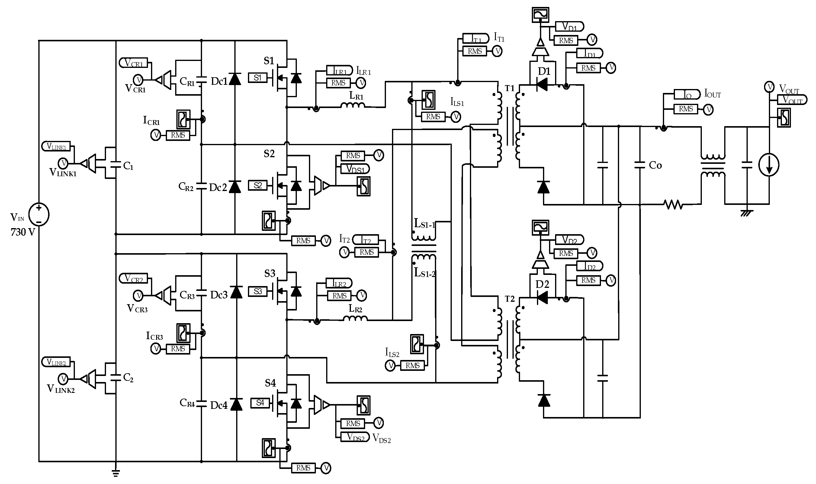
5. Prototype Test and Verification of the Proposed DC/DC Converter

A prototype was fabricated for an experiment in order to verify the proposed resonant LLC converter using a coupled shunt inductor and multiple input transformers. No separate controller was used to solve the problem of power imbalance occurring to the auto-balancing circuit with primary-series and secondary-parallel connection. However, a multiple input transformer was used at each stage to cross different input windings and connect them in series. Accordingly, the magnetizing inductance (LM) of AC resonant tank 1 and 2 could be magnetically coupled. The input voltage was 730 Vdc, the output voltage was 48 Vdc, and the maximum power capacity was 4.8 kW. These were the same as the simulation and design parameters in Table 3. 
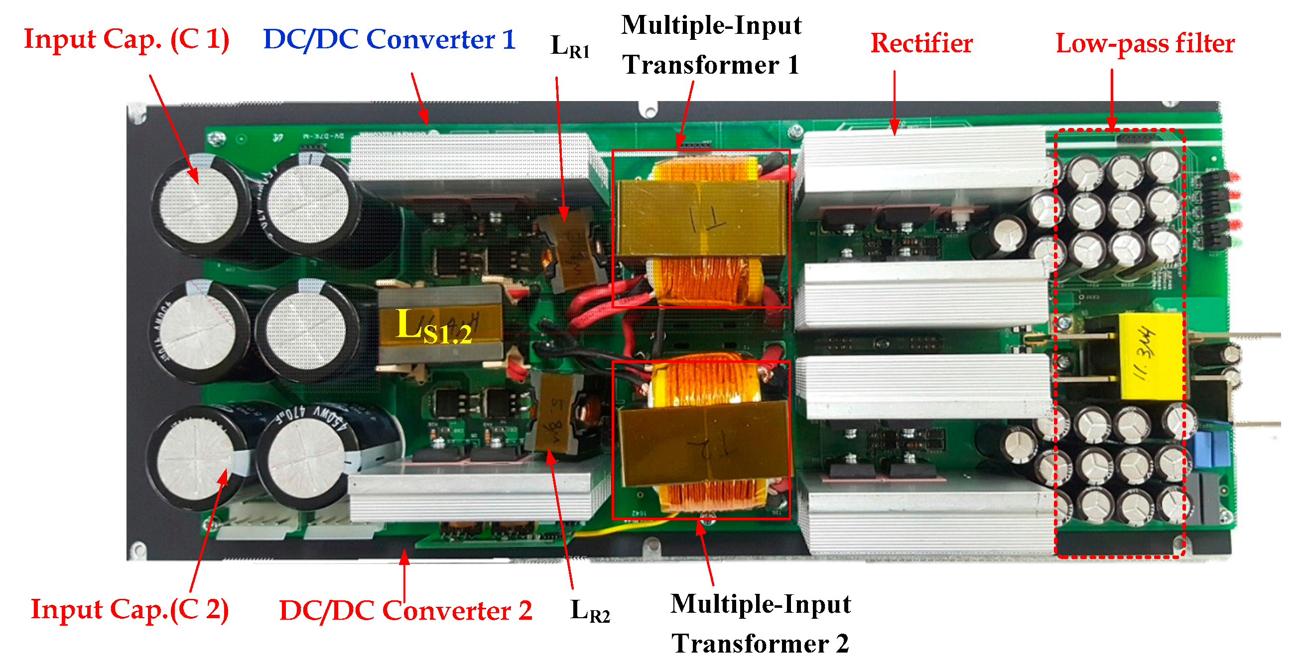
Figure 18 presents the image of the prototype LLC resonant converter using multiple input transformers, which is proposed in this study. The primary side consists of the power conversion units of DC/DC converter 1 and 2, and the rectifiers on the secondary side were configured in parallel.
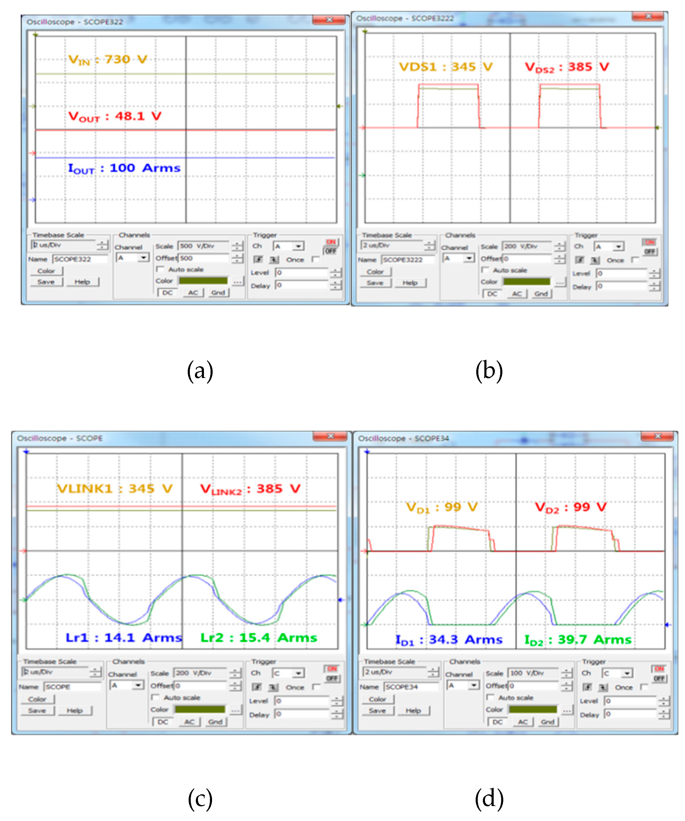
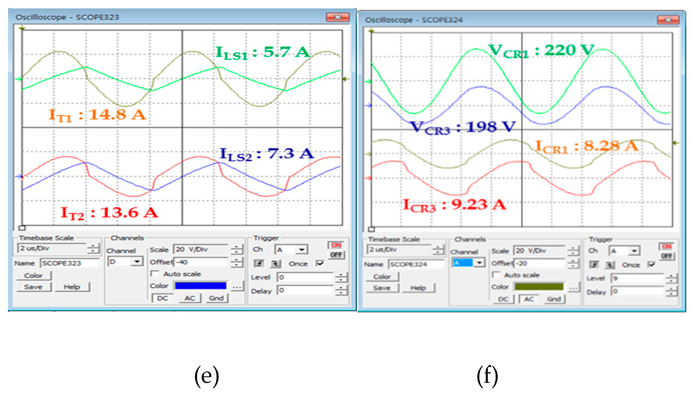
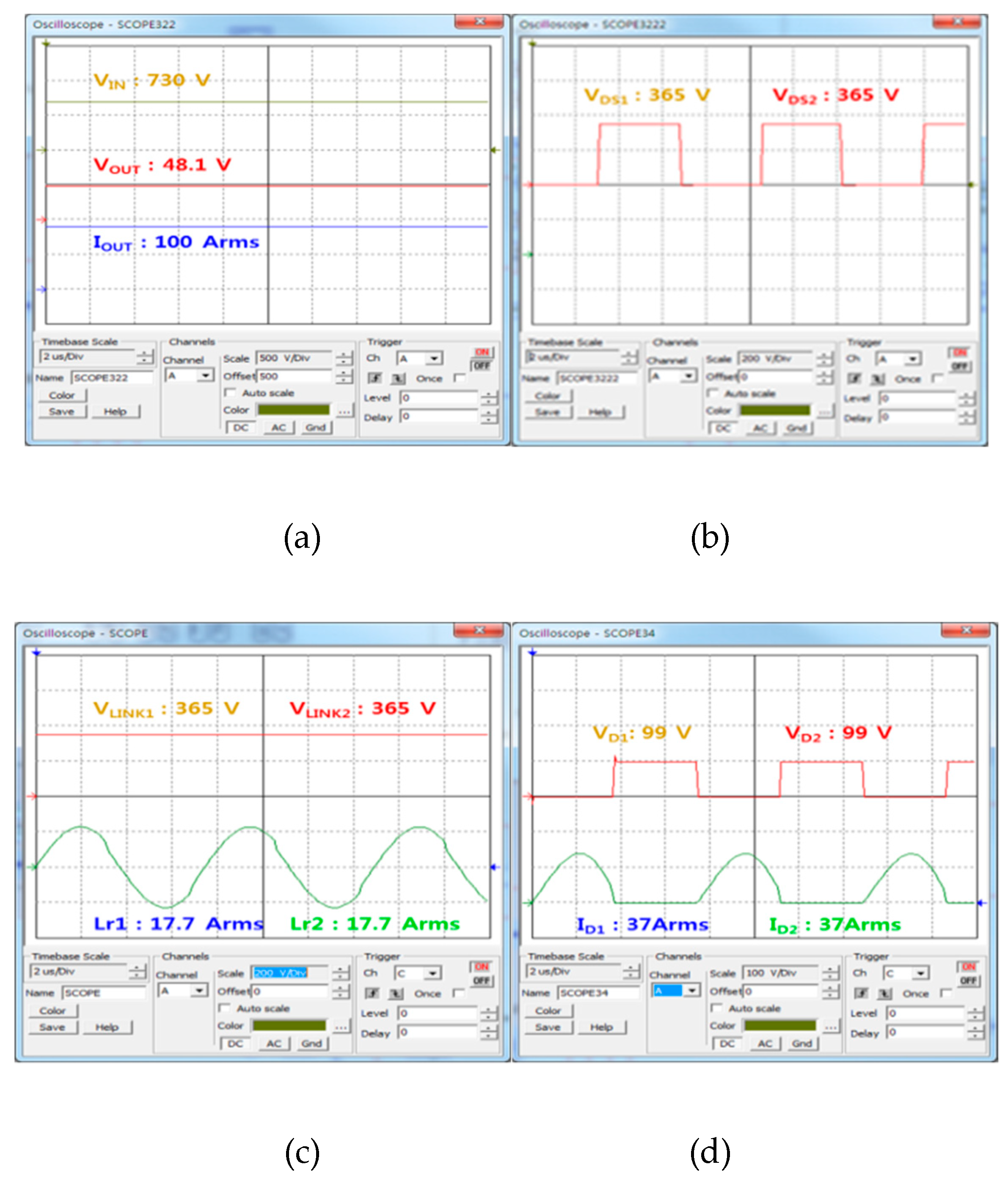
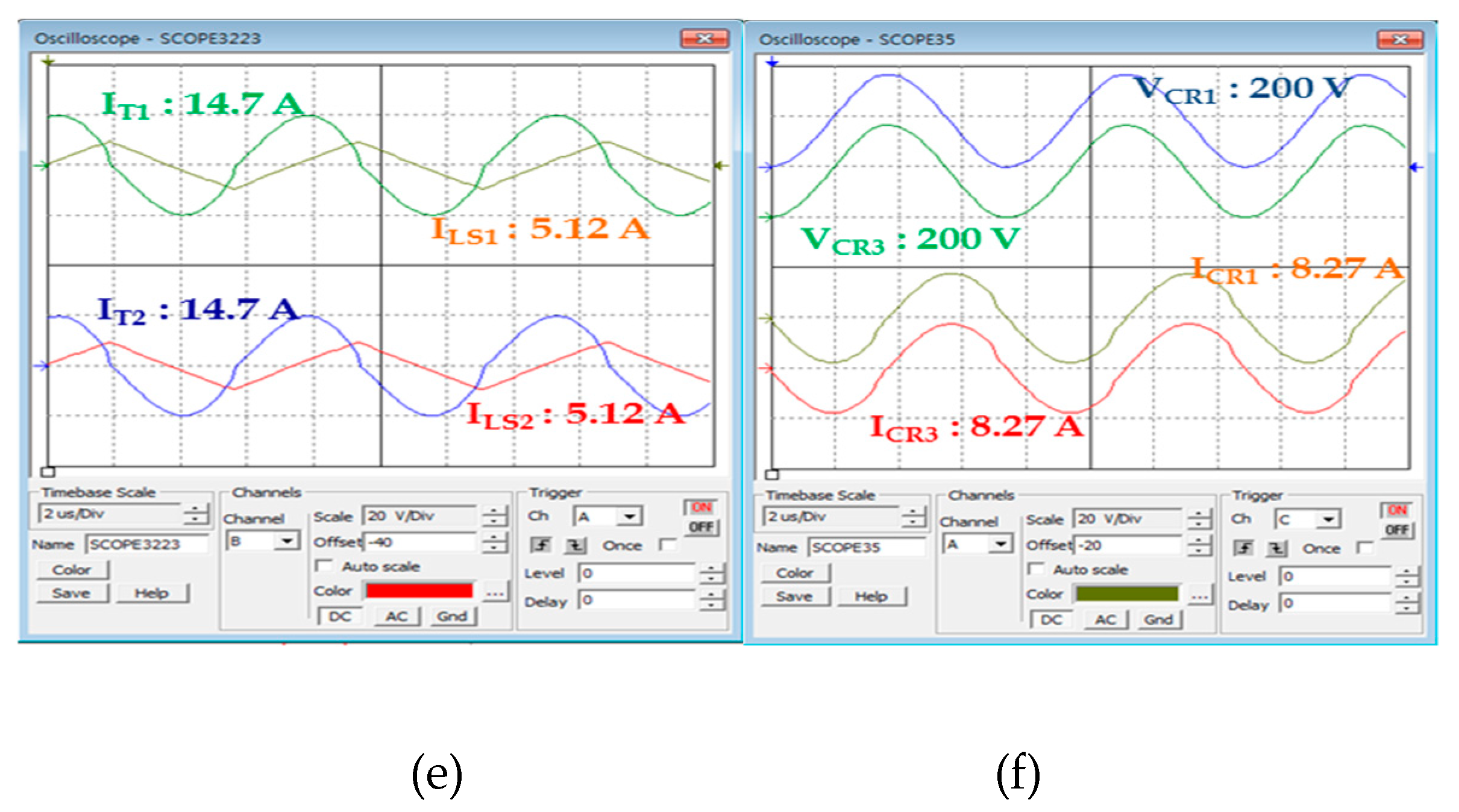
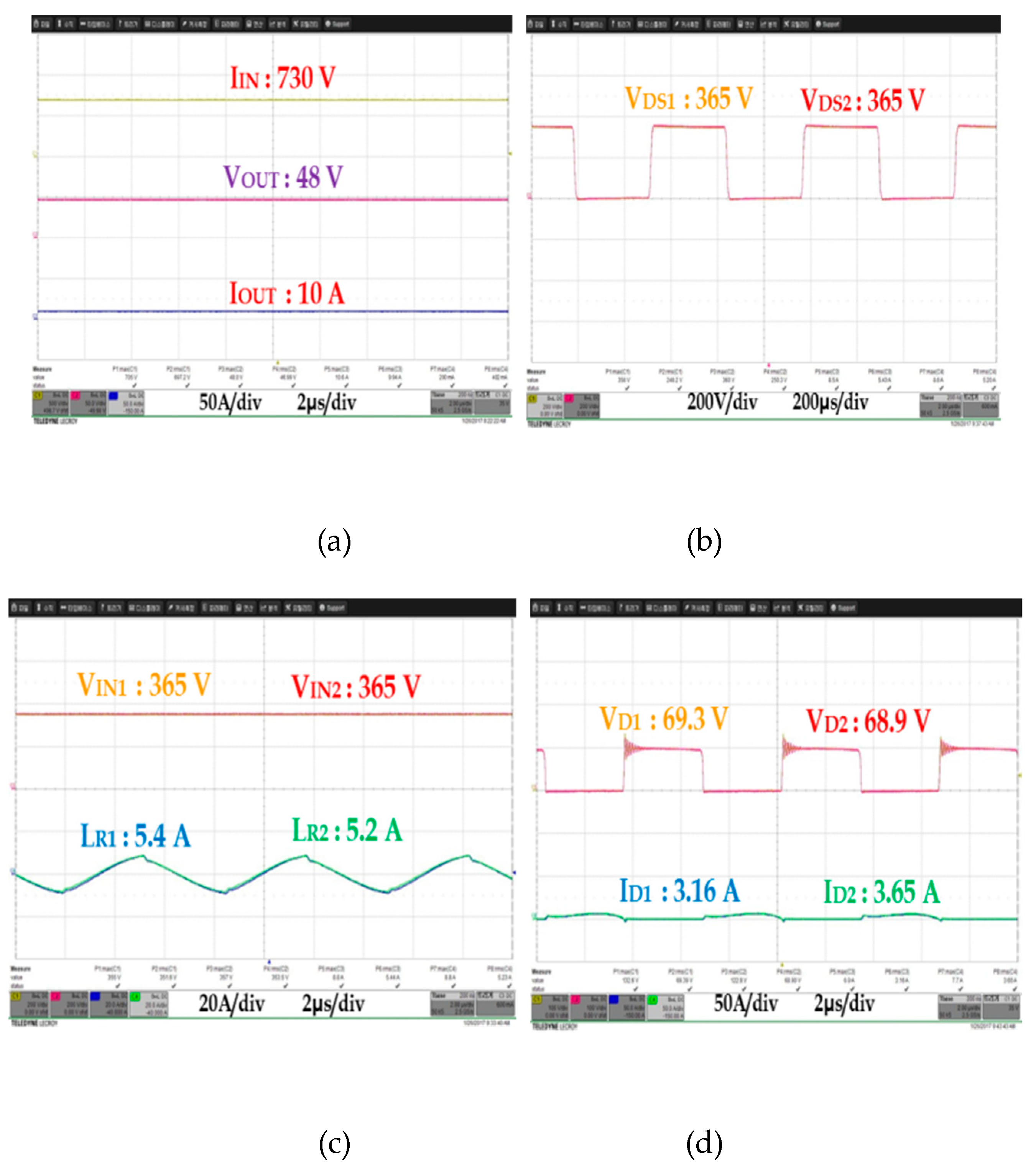
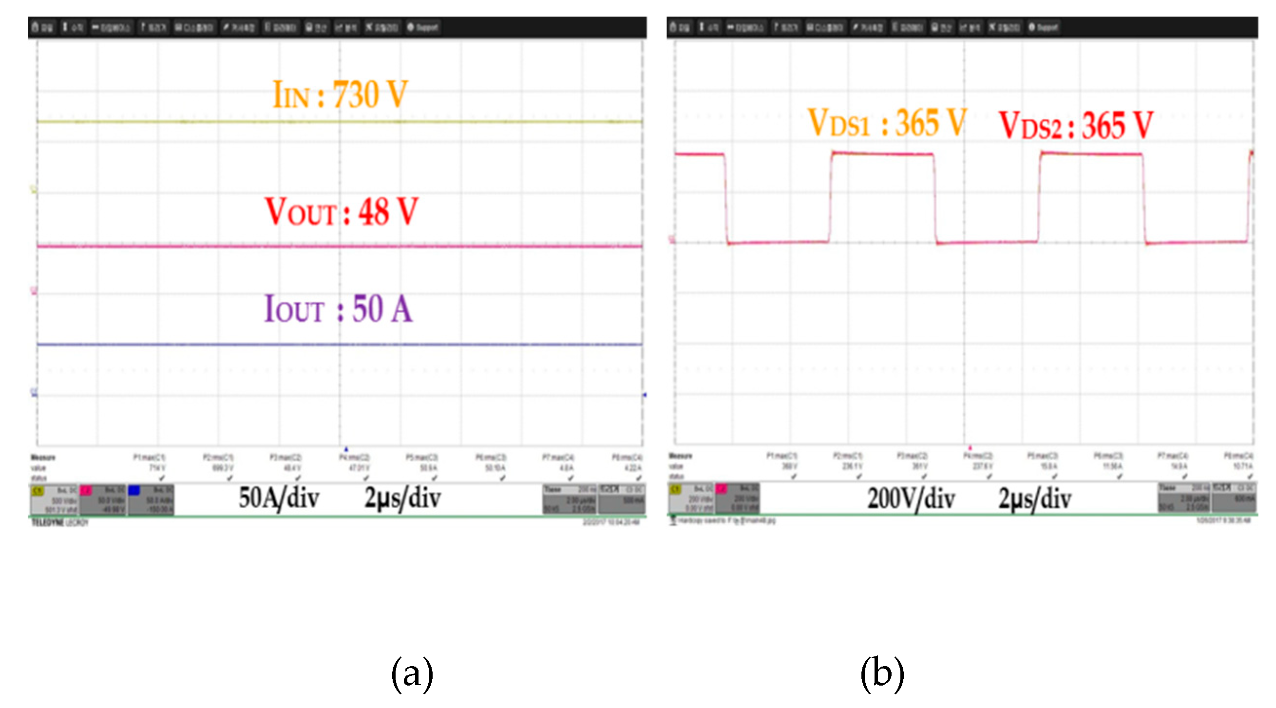
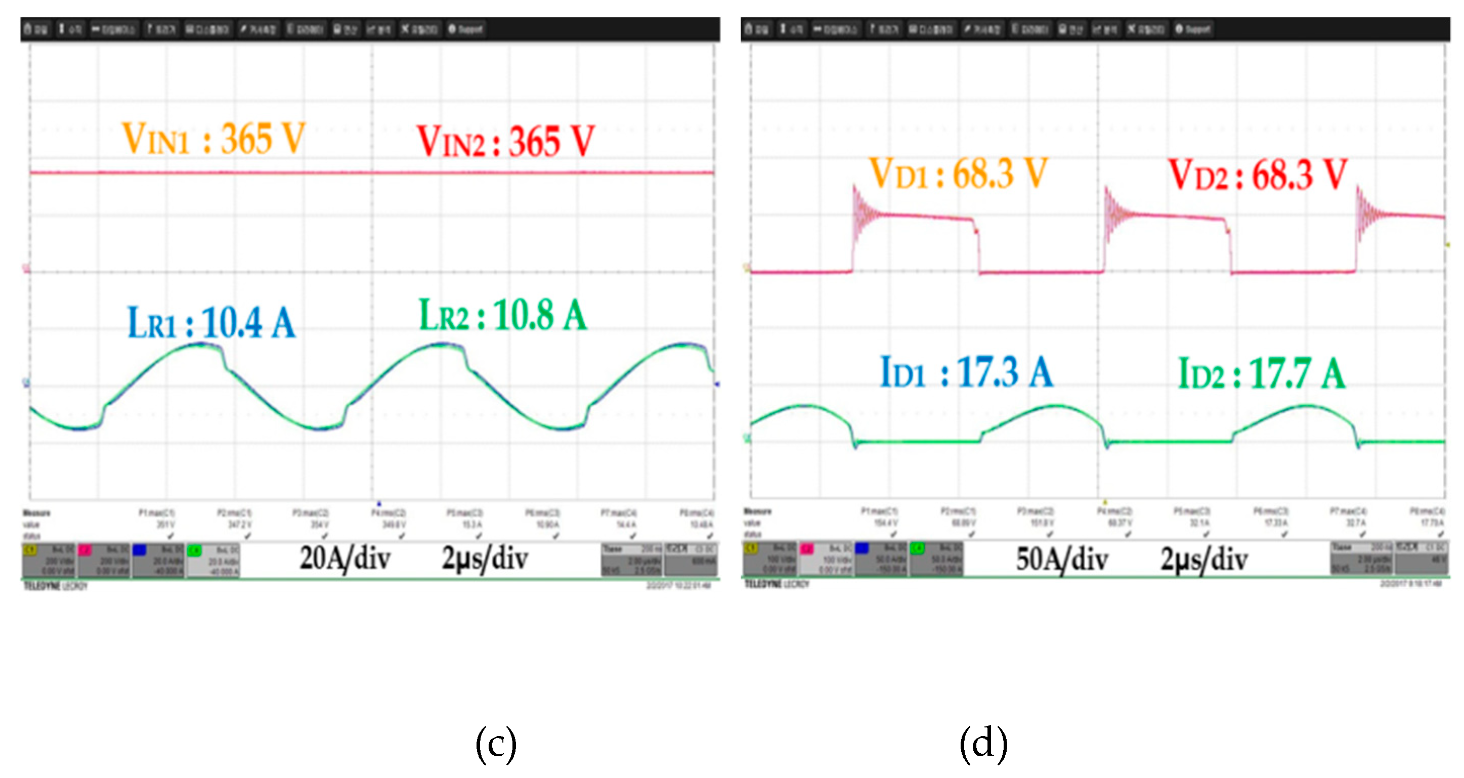
As was in the above simulation, input and output voltages, output current, FET DS waveform (VDS), input capacitor voltage (VIN), resonant current (IR) waveform, and the voltage (VD) and current (ID) waveform of the secondary rectifier diode were measured and compared at 10%, 50%, and 100% load current in order to see whether the power imbalance occurred in DC/DC converter 1 and 2.
Figure 19, Figure 20 and Figure 21 show experimental waveforms obtained under different load conditions. Unlike the simulation result, the waveforms of the proposed converter using multiple input transformers showed a few deviations in input voltage and resonant current. As for such deviations, which were generated in the ideal simulation, the deviation between the resonant capacitor and the resonant inductor, which were used for AC resonant tank 1 and 2, and the deviation of parasite components occurring to PCB design caused an error between input impedance and quality factor (Q), which resulted in a slight power imbalance between DC/DC converter 1 and 2. However, unlike the existing auto-balancing converter, no power imbalance occurred, which is attributable to the deviation between the magnetizing inductance and leakage inductance of two independent transformers. Table 4 presents the comparison result for the input capacitor voltage (VIN), the resonant current (LR), and the voltage (VD) and current (ID) at the secondary rectifier diode of the proposed converter using multiple input transformers. In the experimental results of the proposed ISOP converter, the DC/DC converter 1 and the 2 input capacitor voltage (VIN) are equal to 365 VDC. The resonance tank resonance current (LR) has a deviation of 0.7 A at the maximum load, the secondary rectifier diode voltage (VD) Deviation was 0.4 V, and the diode current (ID) deviation was 0.3 A; it was confirmed that a small deviation occurred.
Table 5 shows a comparison of the major features of the proposed converter and the automatic balancing converter. By using the windings of multiple input transformers crossing each other, the two converters are magnetically coupled to minimize power imbalance. As a result, the core size of the transformer could be reduced from EE7066 to EE6565. The Shunt Inductor uses magnetic inductors in two independent inductors to reduce the deviation and secure the mounting space. As a result, efficiency is improved by 0.7% and power imbalance is minimized by minimizing the heat dissipation area, resulting in a smaller size and an improved power density of 87%.
Simulation results using the PSIM tool show that the power imbalance does not occur. However, the power imbalance in the actual experimental results occurs with the slight error. The experimental results are different because the simulations do not take into consideration the environmental factors such as the deviation of the resonant inductor and the resonant capacitor and the leakage impedance on the actual PCB design.

6. Conclusions

This study has proposed a new circuit for improving the problem of power imbalance by using two DC/DC converters with ISOP structures, where there are a coupled shunt inductor and multiple input transformers sharing magnetic coupling. In addition, both simulation and experiment were conducted for the proposed circuit in order to measure and comparatively analyze the input and output voltage, output current, FET DS switching waveform, DC link capacitor voltage, resonant current waveform, and the voltage and current waveforms of the secondary rectifier diode.
The auto-balancing converter showed a deviation of quality factor (Q) due to the deviation between the magnetizing inductance (LM) and leakage inductance in the shunt inductor and the transformer, which were independently used. Accordingly, DC/DC converter 1 and 2 had different characteristics of input–output voltage gain (M) and input impedance (Zn) at the same frequency, which caused the power imbalance. On the other hand, the proposed topology made DC/DC converter 1 and 2, which used a coupled shunt inductor and multiple input transformers, share the magnetic coupling with each other. Accordingly, no deviation of quality factor (Q) occurred and the input–output voltage gain (M) has the same characteristic as the input impedance (Zn). Thus, it was verified that no power imbalance occurred. As a result, it can be seen that the power imbalance problem of the previous ISPO circuit mentioned in Session 2 is improved using a multi-input transformer that shares magnetic coupling with the combined shunt inductor. The problem of ensuring the breakdown voltage margin of the input capacitor due to the voltage imbalance is improved. The proposed circuit improves the voltage margin and current margin of the switching device due to the voltage rise. The reduced power conversion efficiency is improved due to biased power and thermal issues.
The proposed LLC resonant DC/DC converter is characterized by the magnetic coupling. Therefore, in designing coupled shunt inductors and multiple input transformers, a winding method in which each input winding has the same length to avoid inductance variation should be used. Also, when designing the PCB, the power line for sharing the magnetic coupling of the transformer is complicated, so care must be taken in the design.

Author Contributions

S.-S.H. proposed ideas and implemented and experimented with the system. H.-W.K. was responsible for the elaboration of ideas and comments on research. S.-W.B. was responsible for a basic simulation to validate the proposed idea.

Funding

This research was supported by a grant(19RTRP-B146008-02) from Railroad Technology Research Program funded by Ministry of Land, Infrastructure and Transport of Korean government. This work was supported by “Human Resources Program in Energy Technology” of the Korea Institute of Energy Technology Evaluation and Planning (KETEP), granted financial resource from the Ministry of Trade, Industry & Energy, Republic of Korea (No. 20164030201100).

Conflicts of Interest

The authors declare no conflict of interest.

References

  1. Lai, R.; Wang, F.; Burgos, R.; Boroyevich, D.; Jiang, D.; Zhang, D. Average Modeling and Control Design for VIENNA-Type Rectifiers Considering the DC-Link Voltage Balance. IEEE Trans. Power Electron. 2009, 24, 2509–2522. [Google Scholar]
  2. Araki, J.; Shinozaki, I.; Funato, H.; Ogasawara, S.; Murakami, D.; Hirota, Y.; Mihara, T.; Mouri, M.; Okazaki, F. Verification of LLC Resonant Converter Applied a Current -Balancing High-Frequency Transformer with Multi-Output Windings. In Proceedings of the 2014 International Power Electronics Conference, Hiroshima, Japan, 18–21 May 2014. [Google Scholar]
  3. Mallory, W.D. Dual Input Range Power Supply Tow Series or Parallel Connected Sections with Automatic Power Balancing. US Patent US6370047B2, 9 April 2002. [Google Scholar]
  4. Wang, H.; Chung, H.S.H.; Ioinovic, A. A Class of High-Input Low-Output Voltage Single-Step Converters with Low Voltage Stress on the Primary-Side Switches and High Output Current Capacity. IEEE Trans. Power Electron. 2011, 26, 1659–1672. [Google Scholar] [CrossRef]
  5. Reddy, R. Multilevel Power Converter and Methods of Manufacturing and Operation Thereof. US Patent US8792254B2, 29 July 2014. [Google Scholar]
  6. Lin, B.R.; Nian, Y.B.; Chiang, H.K.; Wang, S.L. New Series Half-Bridge Converters with the Balance Input Split Capacitor Voltages. In Proceedings of the 2014 IEEE International Conference on Industrial Technology (ICIT), Busan, Korea, 26 February–1 March 2014. [Google Scholar]
  7. Nymand, M. Switch Mode Pulse Width Modulated DC-DC Converters with Multiple Power Transformers. US Patent US8743575B2, 3 June 2014. [Google Scholar]
  8. Lee, D.H.; Shin, J.Y.; Hwang, S.S.; Lim, B.K.; Kim, H.W. Analysis of the Efficiency Characteristics of an LLC Resonant Converter having a Current Doubler Rectification Circuit. In Proceedings of the 2015 18th International Conference on Electrical Machines and Systems, Pattaya, Thailand, 25–28 October 2015. [Google Scholar]
  9. Hwang, S.S.; Yoo, Y.D.; Ko, T.J.; Lee, S.T.; Kim, H.W. DC/DC Converter Circuit to Solve Unbalanced Power by Multiple Input Transformers. In Proceedings of the 2017 IEEE 3rd International Future Energy Electronics Conference and ECCE Asia (IFEEC 2017, ECCE Asia), Kaohsiung, Taiwan, 3–7 June 2017. [Google Scholar]
  10. Hwang, S.S.; Yoo, Y.D.; Ko, T.J.; Kim, H.W. The Way of Solution of The Unbalanced Power DC/DC Converter with Multiple Input Transformer. In Proceedings of the 2016 Korea Institute Of Power Electronics Conference, Uiwang, Korea, 25 November 2016. [Google Scholar]
  11. Cho, I.H.; Kim, Y.D.; Moon, G.W. A Half-Bridge LLC Resonant Converter Adopting Boost PWM Control Scheme for Hold-Up State Operation. IEEE Trans. Power Electron. 2014, 29, 841–850. [Google Scholar] [CrossRef]
  12. Yang, B.; Lee, F.C.; Zhang, A.J. LLC Resonant Converter for Front End DC/DC Conversion. In Proceedings of the Seventeenth Annual IEEE Applied Power Electronics Conference and Exposition (IEEE-APEC), Dallas, TX, USA, 10–14 March 2002. [Google Scholar]
  13. Infineon Application Note. Primary side MOSFET Selection for LLC topology, Revision 1.0. 27 June 2014. Available online: https://www.infineon.com/dgdl/Infineon-ApplicationNote_MOSFET_CoolMOS_Primary_Side_MOSFET_Selection_for_LLC-AN-v01_00-EN.pdf?fileId=5546d46147a9c2e40147d3430e927e5d (accessed on 20 November 2018).
  14. Porru, M.; Serpi, A.; Marongiu, I.; Damiano, A. Suppression of DC-link voltage unbalance in three-level neutral-point clamped converters. J. Franklin Inst. 2018, 355, 728–752. [Google Scholar] [CrossRef]
  15. Erickson, R.W.; Maksimovic, D. Fundamental of Power Electronics; Kluwer Academic Publishers: Dordrecht, The Netherlands, 2004; pp. 705–733. [Google Scholar]
  16. AN2450 Application Note. LLC Resonant Half-Bridge Converter Design Guideline. Available online: https://www.st.com/content/ccc/resource/technical/document/application_note/31/fb/59/5e/93/8c/42/b9/CD00143244.pdf/files/CD00143244.pdf/jcr:content/translations/en.CD00143244.pdf (accessed on 20 November 2018).
Figure 1. Commonly used configuration of the power-supply system for communications.
Electronics 08 00352 g001
Figure 2. LLC resonant converter with ISOP auto-balancing connection.
Electronics 08 00352 g002
Figure 3. Equivalent circuit of the auto-balancing LLC resonant DC/DC converter.
Electronics 08 00352 g003
Figure 4. Equivalent circuit of AC resonant tank.
Electronics 08 00352 g004
Figure 5. Input impedance and frequency characteristic graph of the LLC resonant converter.
Electronics 08 00352 g005
Figure 6. Input–output voltage gain and frequency characteristic graph of the resonant converter.
Electronics 08 00352 g006
Figure 7. The proposed DC/DC converter using a coupled shunt inductor and multiple input transformers.
Electronics 08 00352 g007
Figure 8. Equivalent circuit of the proposed AC resonant tank.
Electronics 08 00352 g008
Figure 9. Transformers winding method. (a) Winding of independent transformers, (b) winding of multiple input transformers.
Electronics 08 00352 g009
Figure 10. Simulation circuit of the auto-balancing converter.
Electronics 08 00352 g010
Figure 11. Simulation result for the auto-balancing converter. (a) Input and output voltages and output current; (b) FET D–S switching waveform; (c) input cap. Voltage/resonant current waveform; (d) rectifier diode voltage/current. (e) Ideal Transformer(T1,T2)/shunt inductor(ILS1,ILS2) current waveform; (f) resonant capacitor Voltage(VCR1, VCR2)/resonant capacitor current waveform(ICR1, ICR2).
Electronics 08 00352 g011aElectronics 08 00352 g011b
Figure 12. Input–output voltage gain and frequency characteristics of the auto-balancing converter.
Electronics 08 00352 g012
Figure 13. Input impedance frequency characteristics of the auto-balancing converter.
Electronics 08 00352 g013
Figure 14. Simulation circuit of the proposed converter.
Electronics 08 00352 g014
Figure 15. Simulation result of the proposed converter. (a) Input and output voltage and output current; (b) FET D–S waveform; (c) input cap. Voltage/resonant current waveform; (d) voltage/current of the rectifier diode; (e) ideal Transformer (T1,T2)/shunt inductor(ILS1,ILS2) current waveform; (f) resonant capacitor Voltage(VCR1, VCR2)/resonant capacitor current waveform(ICR1, ICR2).
Electronics 08 00352 g015aElectronics 08 00352 g015b
Figure 16. Characteristics of input output voltage gain and frequency of the proposed converter.
Electronics 08 00352 g016
Figure 17. Characteristics of input impedance and frequency of the proposed converter.
Electronics 08 00352 g017
Figure 18. Prototype of the proposed DC/DC Converter.
Electronics 08 00352 g018
Figure 19. Experimental waveforms of the proposed converter (10% load). (a) Input and output voltage and output current; (b) FET D–S waveform; (c) input cap. voltage/resonant current waveform; (d) voltage/current of the rectifier diode.
Electronics 08 00352 g019
Figure 20. Experimental waveforms of the proposed converter (50% load). (a) Input and output voltage and output current; (b) FET D–S waveform; (c) input cap. Voltage/resonant current waveform; (d) voltage/current of the rectifier diode.
Electronics 08 00352 g020aElectronics 08 00352 g020b
Figure 21. Experimental waveforms of the proposed converter (100% load). (a) Input and output voltage and output current; (b) FET D–S waveform; (c) input cap. Voltage/resonant current waveform; (d) Voltage/current of the rectifier diode.
Electronics 08 00352 g021
Table 1. Power imbalance characteristics of the auto-balancing converter.
Load (A)ZIN1 (Ω)ZIN2 (Ω)VIN1 (V)VIN2 (V)POUT2 (W)PUOT2 (W)
07.578.77337393--
503.883.923633671,1521,248
1002.212.463453852,2082,592
Table 2. Input balance characteristic of the proposed converter.
Load (A)ZIN1 (Ω)ZIN2 (Ω)VIN1 (V)VIN2 (V)POUT1 (W)POUT2 (W)
08.178.1736536500
503.903.9036536512001200
1002.342.3436536524002400
Table 3. Parameters for comparative analysis of DC/DC converters.
Input Voltage730 Vdc
Output Voltage48 Vdc
Output Current100 A
Switching Frequency110~180 kHz
Resonant Frequency140 kHz
CR/LR234 nF/5.4 µH
C1, C21410 µF (470 µF × 3)
R1, R2100 kΩ
LM37 µH (@ design value)
LM (±10%) Deviation32.4 µH39.6 µH
Table 4. Balance characteristics of the proposed converter at each load.
Load (A)VIN1 (V)VIN2 (V)LR1 (A)LR2 (A)VD1 (V)VD1 (V)ID1 (A)ID2 (A)
103653655.45.269.868.93.163.65
5036536510.410.868.368.317.317.7
10036536518.218.968.568.935.135.4
Table 5. Comparison of Proposed Converter and Automatic Balancing Converter.
Auto Balancing ConverterProposed ConverterRemarks
TransformerIndividual transformer, 2ea
Core: EE 7066
Multiple-Input Transformers, 2ea
Core: EE6565
Core Size↓
Shunt InductorIndividual Inductor, 2eaCoupled Inductor, 1eaMagnetic sharing
Size9.3′(W) × 17′(D) × 3.5′(H)7′(W) × 17′(D) × 2.5′(H)
Power density8.62W/in316.13W/in387%↑
Efficiency97.2%97.9%0.7%↑

