Article

A True Process-Heterogeneous Stacked Embedded DRAM Structure Based on Wafer-Level Hybrid Bonding

1
School of Microelectronics, University of Science and Technology of China, Hefei 230026, China
2
Xi’an UniIC Semiconductors, Xi’an 710075, China
3
Institute of Microelectronics of the Chinese Academy of Sciences, Beijing 100029, China
4
School of Microelectronics, University of Chinese Academy of Sciences, Beijing 100029, China
5
Faculty of Electronic and Information Engineering, Xi’an Jiaotong University, Xi’an 710049, China
*
Author to whom correspondence should be addressed.
Electronics 2023, 12(5), 1077; https://doi.org/10.3390/electronics12051077
Submission received: 16 January 2023 / Revised: 8 February 2023 / Accepted: 16 February 2023 / Published: 21 February 2023
(This article belongs to the Special Issue Interconnects for Electronics Packaging)

Abstract

:
In response to the increasing manufacturing complexity/cost in maintaining DRAM advancements through traditional scaling, three-dimensional integrated circuits (3D ICs) and 2.5-dimensional ICs with Si interposers are known as promising candidates to overcome these challenges due to their advantages of low power, small form factor, high density, and high bandwidth. In this work, we present a true process-heterogeneous stacked embedded DRAM (SeDRAM) using hybrid bonding 3D integration process, achieving high bandwidth of 34 GBps/Gbit and high energy efficiency of 0.88 pJ/bit. Moreover, the critical factors of the SeDRAM design are presented (e.g., the low data movement energy, high-density physical interface, simplified protocol definition, process compatibility, density extensibility, and hybrid bonding connection fast test by DFT (design for test). Our results and design methodology have paved the way to realize applications of hybrid bonding to high bandwidth and energy efficiency DRAM. More importantly, the SeDRAM solution can also support the maximum storage density of 48 Gbit and the bandwidth capability of TBps. It can greatly alleviate the “memory wall” problem and thus improve its competitiveness in near-memory computing/computing-in-memory fields.

1. Introduction

DRAM has been developed for approximately a half century. It is still the main memory in modern computer systems because of its relatively low latency and high density. As a memory, its major breakthrough is the density increase which is extremely dependent on process scaling. Nevertheless, further scaling of DRAM has become difficult due to manufacturing complexity/cost [1,2]. Meanwhile, increasing DRAM bandwidth through speeding up the data transferring and increasing data parallelism is catching up with modern computing development, especially the AI computations that require more data and keep demand booming [3]. Moreover, the data movement energy consumption of off-chip memory solutions is orders of magnitude greater than that of on-chip memory, resulting in the well-known “memory wall” problem [4]. Near-process memory built with logic-to-DRAM hybrid bonding has been used to solve the “memory wall” problem [4].
Currently, the graphics double-data rate SDRAM (e.g., GDDR6/6X [5,6]) is one of the primary solutions to develop high bandwidth DRAM. GDDR SDRAM is common in traditional graph acceleration, which has the maximum data transferring speed. The technical methodology of the GDDR SDRAM overlaps DRAM accesses in different banks to match the I/O frequencies [7]. Comparatively, GDDR SDRAM takes more than 50% of the energy for high-speed data transfers, especially in the PCB (printed circuit board) path. Therefore, energy efficiency and thermal management are immediate challenges to be addressed by GDDR DRAM in the future [7].
New solutions have been proposed using wide I/O with lower speed, such as high-bandwidth memory (HBM), to improve the performance of the memory interface. HBM uses TSV (through-silicon vias) structure with microbump stacking and interposer technologies enabling multiple chip stacks and wide I/Os between the processor and memory, thereby providing high capacity, low power, and high bandwidth [8,9]. HBM uses silicon interposers to implement the wide data connection. The silicon interposer is the key to achieving less cross-talk during high-speed data toggling and less energy loss in data transferring. Furthermore, a scalable interconnect is a necessary component for an interposer-based system to make full use of the high bandwidth of multiple HBM DRAM stacks [10,11].
However, the conventional 3D integration process with bumps is limited by Si thickness reduction and interconnection density due to the bump size. Furthermore, microbump stacking and interposer connections are challenged by large resistance, heavy capacitance, bump-to-bump short failures, and a limited number of stacking levels [12,13,14]. Moreover, complex and power-hungry PHY (physical layer) circuits in both HBM and logic sides are also challenges to consider [1].
Based on three-dimensional integrated circuit (3DIC) technology maturity, it is time to develop high-bandwidth DRAM with high energy efficiency. Compared with commercialized HBM using TSV and microbumps, hybrid bonding can provide much less parasitic capacitance and resistors for higher energy efficiency DRAM [1,15].
SeDRAM was introduced in [1] as the first HB based 3D integration process implementing a heterogeneous architecture between logic die and DRAM die.Since the introduction of SeDRAM, applications based on SeDRAM, for example near-process memory [4], have been developed. Furthermore, more challenges with SeDRAM have been addressed to enable SeDRAM to increase its performance, lower the energy consumption, and be adopted to a wider range of applications. This manuscript illustrates more details on SeDRAM design and describes some new developments of SeDRAM listed in the following section:
  • Data Movement Energy
Generally, the energy consumption of DRAM occurs in activation and data movement, and the data movement is the major energy consumer. Furthermore, the energy consumption of data movement is mainly concentrated in the data buffer and transfer wiring. Reducing the distance of data transfer can decrease the parasitic capacitance and required buffer size. However, DRAM always chooses the appropriate chip size to trade- off chip yield, cost, and energy efficiency. Here, the high energy efficiency of SeDRAM can be achieved by shorter data transfer distance and improved data buffer, which means that the data buffer location and driver size are the key points during design.
  • Physical Interface
Combined with the advantages of the hybrid bonding of less parasitic capacitance and resistors, the proper placement of the physical interface by the z-axis direction needs comprehensive consideration. For example, master I/O (MIO) is a possible interface between DRAM and logic; even an MIO network can be implemented in DRAM or logic. Additionally, MIO provides flexibility in the placement of sense amplifiers. It can reduce the distance of data transfer by setting hybrid bonding to the physical interface of MIO in the z-axis direction. Therefore, hybrid bonding can be used as a physical interface through the z-axis direction, providing more possibilities for improving DRAM performance.
  • Protocol Definition
Compared to SRAM, which has explicit write and read definitions, DRAM has one more activation operation. To reduce the integration complexity of the proposed SeDRAM, asynchronous operation can be the choice. Moreover, asynchronous operation can reduce the latency of write/read access. Through application in logic, whether to synchronize the data or not can easily be decided.
  • Density Extensibility
Density extensibility capability enables memory to more easily meet diverse application demands. The array die consists of a repeatable memory unit of 1 Gb, and multiple configurations of the SeDRAM array die can be achieved in a wide density range of 1 Gb–48 Gb. The upper limit of storage capacity depends on the maximum exposure size of the reticle. Moreover, unlike conventional plane DRAM, SeDRAM uses two wafers stacked, and hence, the reticle alignment design is the key to accurate alignment and integration.
  • Process Compatibility
The new DRAM structure is compatible with traditional DRAM manufacturing processes, including metal, cell efficiency, and subarray size definition. The minor periphery adjustment of DRAM is important for this work.
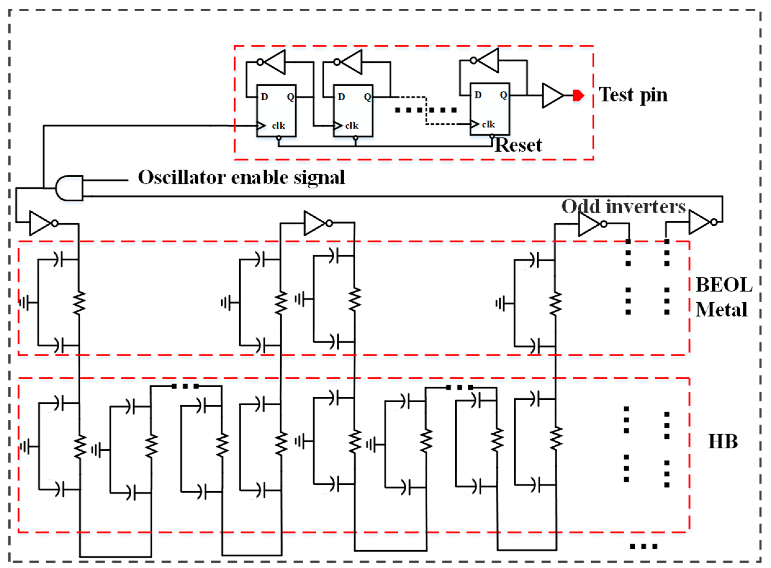
  • Hybrid Bonding Connection Fast Test
Given hybrid bonding process complexity and high hybrid bonding connect density, we must find a fast and low-cost way to locate bad connections. The hybrid bonding density even in a small-scale system is on the order of tens of thousands. Testing all the connections becomes very challenging when considering area and test time. Moreover, the logic part used for testing has a negative impact on the original interface timing. Thus, we put forward a test method of a hybrid bonding ring, which makes a ring of specially tested hybrid bonding around the hybrid bonding of the key signals.
The SeDRAM with an SRAM-like interface features competitive energy efficiency, low latency, high bandwidth, and easy integration. Contrary to the traditional DRAM, the SeDRAM solution connects the DRAM chip and ASIC (application specific integrated circuit) chip on PCB, which can reduce the PCB connection and save PCB space and has an easy ASIC design due to no need for a complex PHY. Meanwhile, it achieves higher bandwidth when all banks in the RAM can be accessed simultaneously by the SeDRAM solution.
In this proposed SeDRAM, the periphery circuits, including control, I/O, and DFT, are separated and placed on a logic die. A metal interconnection process for bonding Cu pad was carried out on the already fabricated logic die and another DRAM array die. The DFT block is designed as an IP in the logic die to perform BISR (built-in self-repair) for the array die. Hybrid bonding process offers a z-axis direction of integration, enabling new 3D SeDRAM architectures to benefit from the respective enhanced performance of independent logic and array die process. This approach paves the way for a special interface and high density of DRAM by adding innovative features to the logic die.
The hybrid bonding density in this work is up to 110,000/mm2 due to a 3 µm fine pitch, which is hundreds of times denser than the microbump density in HBM. Moreover, hybrid bonding has a low resistance of less than 0.5 ohm/ea, so the energy consumption of the logic-to-memory interface can be reduced by 40% [1].
We have successfully developed a platform with 1 Gbit SeDRAM, which provided 1024 I/O, a speed of 266 MHz, a bandwidth of 34 GBps, and a power efficiency of 0.88 pJ/bit. In the meantime, the SeDRAM solution can also support the storage density of 1/2/ 3/4 G/6/8/12/24/36/48 Gbit and bandwidth in TBps. In summary, this paper makes the following contributions:
  • We propose a new DRAM architecture, SeDRAM, which provides extremely high energy efficiency and a simplified local data interface.
  • We develop the bandwidth extension method based on the 3DIC process, which guarantees maximum bandwidth reach to TBps pre-chip.
  • We put forward the fast test method for hybrid bonding (HB) connections.
The rest of the sections are organized as follows. Section 2 describes the architecture and HB process detail of the SeDRAM. Section 3 provides a brief concept and description of the HB connection fast test. Section 4 discusses the results for the LPDDR4 based on SeDRAM and HB connect. Section 5 summarizes the overall work.

2. SeDRAM

We propose a stacked embedded DRAM (SeDRAM), which is a new DRAM solution for high-bandwidth memory platforms (Section 2.1). A logic die and a DRAM array die are stacked together using HB technology (Section 2.2). A logic-to-DRAM interface is defined to realize the full potential of our proposed solution.

2.1. SeDRAM Architecture

Figure 1 illustrates the structure of the proposed SeDRAM chip. There is a logic die facing downward at the top and an array die at the bottom. All control logics and I/O circuits are on the logic die. The density of each SeDRAM unit is as high as 1 Gb, which is much higher than a single embedded SRAM instance of less than 1 Mb. The array die is built up with a repeatable memory unit of 1 Gb, which consists of eight array blocks of 128 Mb and an independent on-chip power system. The DRAM array uses long BL and long WL schemes in the cell array to maximize cell efficiency, featuring 688 cells per BL and 1142 cells per WL. The array block is based on a trade-off between density and bandwidth. The 128 Mb density is the most area-efficient partition to support a 128-bit pre-fetch scheme for high bandwidth. Each 128 Mb array block is an independent memory channel with individual control and data signals: row address (RA), bank active (BNKSELb), column address (CA), write control (CASWR), read control (CASRD), and 128-bit read/write data line (RWDL). Since all memory channels can be accessed simultaneously, the total bandwidth is widened by high-channel-level parallelism in SeDRAM. Compared to HBM, the bandwidth of 1 Gb SeDRAM can reach 34 GBps, even if the data rate runs as low as 266 MHz. The low data rate is common in the history of DRAM. Limited by the principle of density first in the DRAM industry, vendors prefer increasing DRAM density instead of decreasing latency in the course of DRAM technology evolution.
Comparatively, the active/write/read control signals are shared between banks in conventional DRAM, but those of each bank (called “channel”) are independent in SeDRAM. Otherwise, the row/column control blocks in each bank are almost identical. Moreover, the RWDL is a shared data bus between banks and peripheral circuits in a conventional DRAM. In SeDRAM, the data bus is individual for each channel. Since the RWDL is a full-swing logic signal, it is suitable to serve as the internal digital signal to the logic die. There are two other advantages: (1) RWDL is already finished the data bus merging, and it is highly efficient in the power supply network for the signal driver. It is also friendly for logic integration. (2) It almost does not touch the original array interface design, more robust timing margin during write/read.
Based on the same memory density (e.g., 1 Gb), it is possible for SeDRAM to achieve much higher bandwidth with much reduced I/O power consumption simultaneously than HBM by stacking the logic wafer and array wafer and developing a fine-pitch hybrid bonding technology.

2.2. Hybrid Bonding Technology

Wafer-to-wafer HB technology [15] is used to realize a DRAM array wafer and a logic wafer face to face connected with the advantages of a high density integration for high bandwidth and energy efficiency. Our proposed SeDRAM process is shown in Figure 2. First, logical die and array die were prepared and finished the top metal respectively. Second, hybrid bonds were performed in each logic/array wafer, where top vias (TVIA) and bottom vias (BVIA) are involved by planarization, photography, and dry etch processes. Third, the two-processed logic and array wafer were bonded face to face by hybrid bonding. After that, the Si substrate of the logic wafer was thinned to about 3 µm. Finally, the PAD out window was opened from logic wafer backside. The HB pitch size is 3 µm; by contrast, the pitch of the microbump was approximately 50 µm and the pitch of TSV was approximately 6 µm [16]. Although a smaller pitch of HB is available, 3µm of SeDRAM is already comparable to the pitch of the top metal and sufficient to reliably transfer signals between array wafers and logic wafers with minimum area penalty in mass production.
Figure 3 shows the SeDRAM cross-sectional TEM image. Compared to HBM using microbump and TSV technologies, SeDRAM using hybrid bonding technology can reach a maximum through the density of 110,000/mm2.

2.2.1. Hybrid Bonding Integrity

The HB pitch is 3 µm. Therefore, we have built an HB via an array aligned to RWDL, which is usually centrally arranged in the array die. To mitigate the power consumption concentration at the interface, another HB via an array for power supply should be constructed. Finally, a module of those HB via array is defined to improve reuse ability and integration efficiency. We confirm the correctness and accuracy of the HB module design by layout-versus-schematic (LVS) and design-rule checking (DRC) checks, respectively. Moreover, we use a twin-via structure to improve the interconnection reliability in the design phase.
Special align marks are used for accurate HB interconnection of logic and array wafers in the fabrication phase. Multiple marks have been placed in the logic wafer and array wafer to provide sufficient bonding overlay in the worst case.
Thanks to the robust HB connectivity and stable backend metallization process, the fabricated SeDRAM can reach the same yield as the existing DRAM products even if the HB process is added to the DRAM manufacturing process. However, any failure by voids or overlay misalignment of the HB is fatal. Additional procedures are still necessary to scan the HB integrity in the test phase to screen out failed connections.

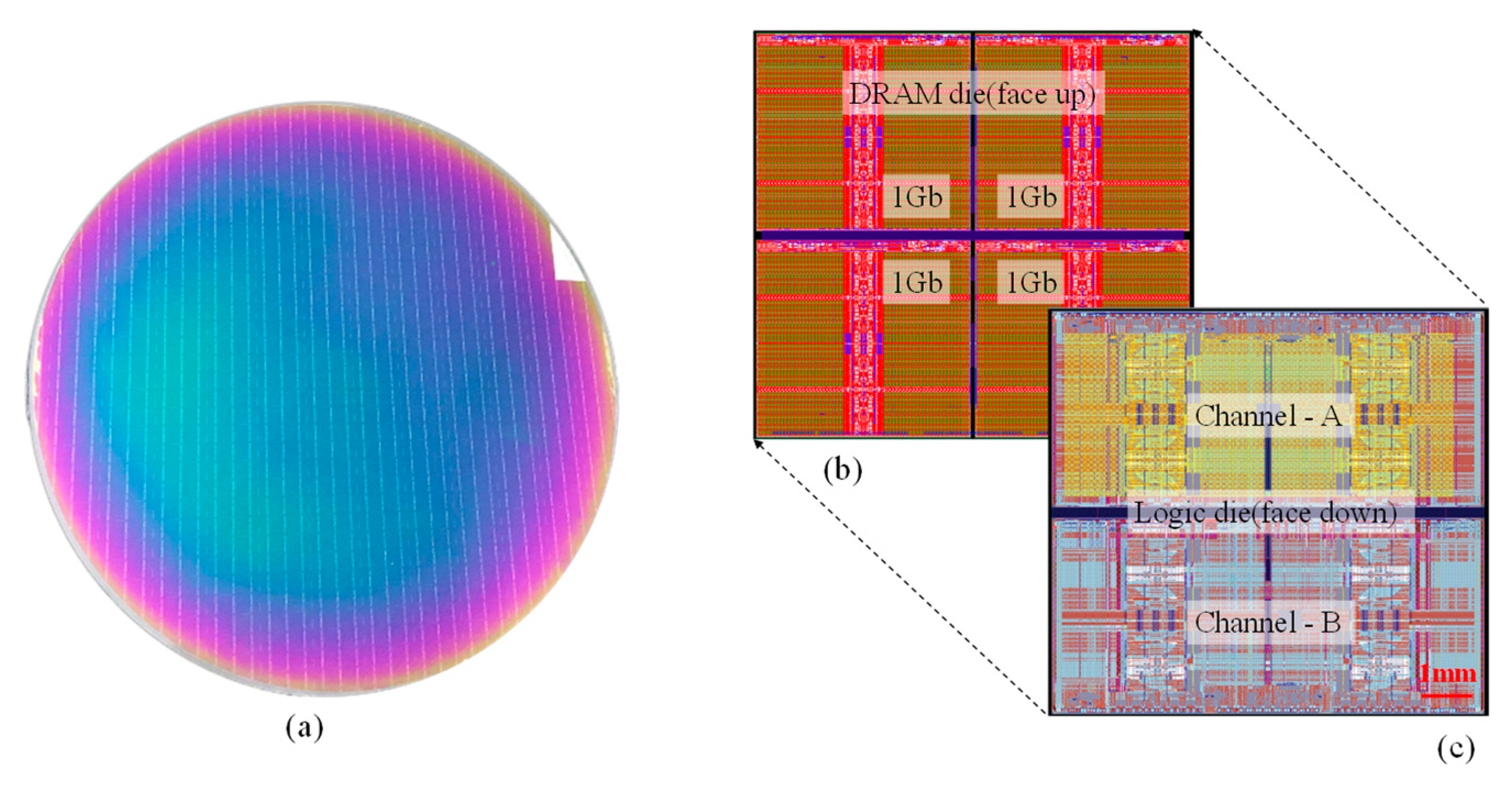
2.2.2. Reticle Design

The array die is built up with a repeatable memory unit of 1 Gb. On this basis, multiple configurations of the SeDRAM array die can be achieved in a wide density range of 1 Gb–48 Gb. The density is only limited by the maximum exposure size of the reticle. The users should take the flexibility of density configuration in fine granularity.
Many-core SoC is suitable for full utilization of high bandwidth of SeDRAM for high parallel access. Figure 4 is an example of a 36 Gb SeDRAM die and corresponding logic die. The logic die is a 3 × 3 mesh network-on-chip (NoC) with 55 nm technology. It has 288 processing elements, each of which independently accesses its memory bank separately. The array die consists of 6 × 6 memory units. The size of the logic die and that of the 36 Gb array die are identical. The 6 × 6 configuration of SeDRAM is based on the SoC computing requirement and the manufacture limitation of exposure size.
Regarding 3D stacking design in SeDRAM, the reticle design is the basis to ensure that the two wafers can be accurately aligned and integrated. First, align marks are denoted on logic and array dies. Second, scribe lines in the array die support memory re-partition by requirement. Third, the misalignment between the Cu bond pads should be as small as possible, which relies on the reticle design to ensure alignment.

2.2.3. Logic-to-DRAM Interface

Compared with conventional HBM interconnection structure, our proposed structure removes time-consuming and power-consuming PHYs from both the DRAM array die and the logic die, as shown in Figure 5. Because conventional DRAM is limited by the number of transfer channels and need S2P (serial to parallel) and P2S (parallel to serial) for the data recombination, it costs additional time and power. Meanwhile, conventional DRAM applications need off-chip drivers to achieve data movement and hence also cost additional time and power. Our proposed SeDRAM structure supports almost unlimited signal channels and nearby memory controllers. Therefore, it can save a lot of time and power consumption. The hybrid bonding density is a few hundred times denser than the microbumps used in HBM. Consequently, the logic-to-DRAM interface offers a high bandwidth interconnection with relatively high energy efficiency [4,17,18].
First, we introduce an SRAM-like interface to fully utilize the advantages of low latency and high energy efficiency. The interface runs at the clock rate of several-hundred-MHz level. After the selected page is activated, write operation (WR) and read operation (RD) are triggered by write and read clocks, respectively. As shown in Figure 6, after the selected page is activated by bank selection signal (BNKSELb) and RA accordingly, WR and RD are triggered by write and read clocks (CASWR for WR and CASRD for RD), respectively. The write and read clocks are 3.76 ns in period, and the interface data rate is up to 266 MHz, which is equivalent to a bandwidth of 34 GBps/Gb (266 MHz ×128 b × 8). Additionally, the total latency from read clock (CASRD) to data (RWDL) is suppressed to as low as 6 ns, compared to more than 10 ns for conventional DRAM. Although the delays of an array, sense amplifier, and internal data transportation remain, the data line is shortened and PHY is removed from the array die.
Second, we have designed a complete power system, including band gap, pump, and linear generators, in an array die to generate various voltages for cell operation internally. The external powers of an array die are reduced to two parts: (1) VDD1 = 1.8 v for array-related power supplies and (2) VDD2 = 1.1 v for data transportation, improving the power supply efficiency and the energy consumption at the wide data interface.
Overall, the logic-to-DRAM interface consists of an SRAM-like interface for normal operation and a compact power supply interface. Additionally, a DFT IP is provided to be integrated into the logic die for array die test and repair. The DFT IP shares the buffer with a normal interface. Detailed information regarding the DFT IP is discussed in Section 2. Users must follow integration guidelines to guarantee the functionality and reliability of SeDRAM.

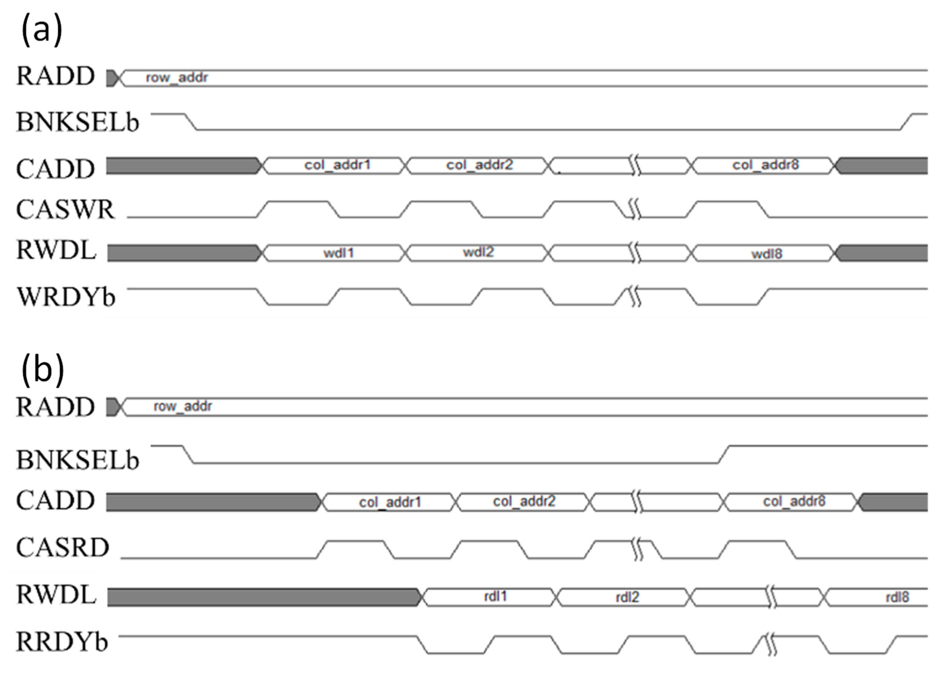
3. Hybrid Bonding Test in SeDRAM

Memory test and repair are essential for DRAM applications. A set of tests is manually optimized for the particular technology to obtain economically acceptable test times. The question is how effective these tests are. The test concept is discussed here to guarantee the fault coverage and repair ability of SeDRAM, especially HB integrity. A soft IP is provided for SeDRAM DFT, integrated into the logic die and already has been silicon-proven (Section 3.1). Both indirect and direct methods are sufficient for the HB test (Section 3.2). A fast test methodology is proposed by making a ring of specially tested HB around those of the key signal to reduce test cost (Section 3.3).

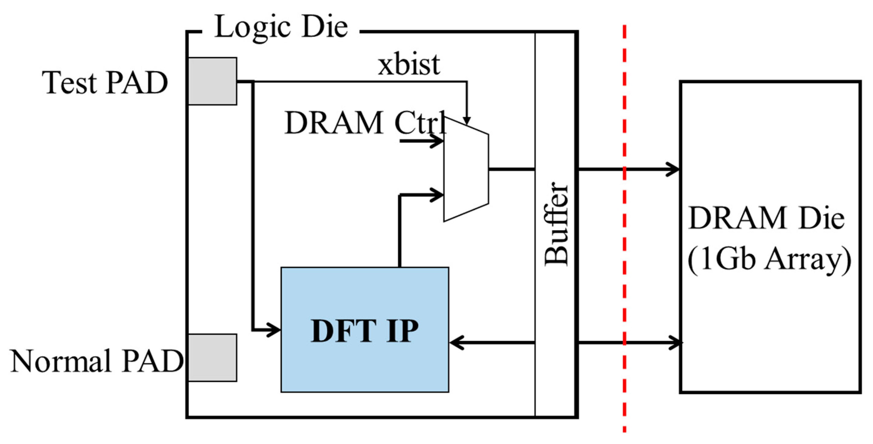
3.1. DFT IP for SeDRAM

Abundant e-fuses are located on the array die with supporting circuits for sensing and burning. Some fuses are used for memory repair, and others are used as test modes for chip configurations. Moreover, a DFT IP is designed as a soft IP in the logic die to perform BISR for the array die. Many works [19,20] have been done on designing memory tests to detect various faults for coverage. An on-chip serial protocol is implemented in the DFT IP to transfer and set the value of fuses. The final repair solution is formulated and burned into the e-fuses. Because the DRAM-specified tests have been integrated into the DFT IP, users can freely use the SeDRAM just like SRAM.
As shown in Figure 7, the DFT IP is integrated into the logic die for array die test and repair. Since the DFT IP shares the buffer with normal control blocks, we can control the multiplexer by external test pad to switch SeDRAM between normal operations and DRAM test operations. The DFT IP not only performs memory test and repair the same as normal DRAM but also tests HB integrity for 3D stacking of SeDRAM. Especially, dedicated test procedures are designed to screen out failed HB structures to guarantee connection integrity.

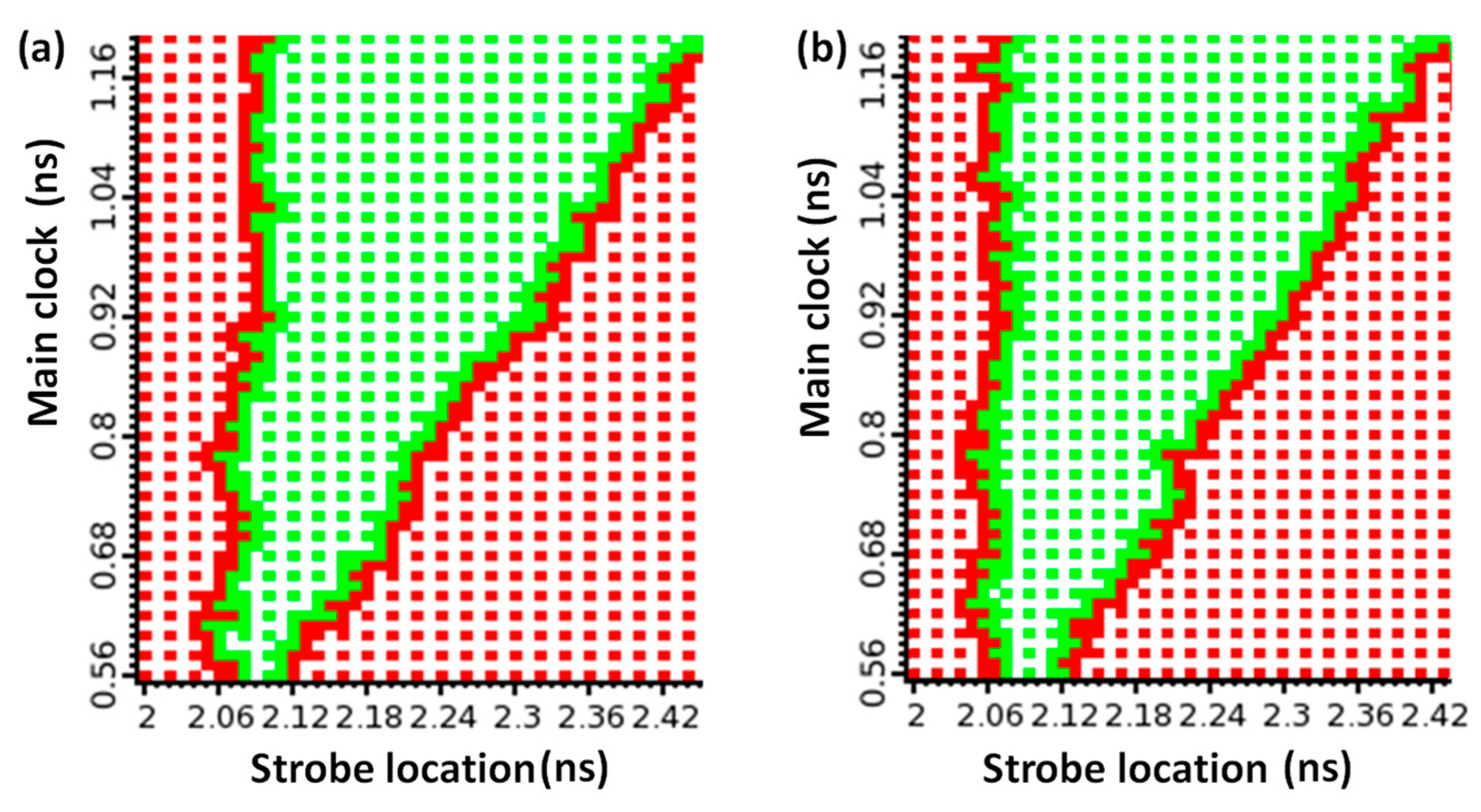
3.2. Indirect and Direct Test of Hybrid Bonding

The 3D IC stacking technology using HB has absolute advantages in system bandwidth, integration, and power consumption. However, the HB process is challenging, ensuring that all HB connections are perfect in manufacturing is difficult. Because HB connectivity directly affects the success of chip stacking, the chip yield variation, due to the HB process, can be monitored in mass production [21]. Comparatively, existing DRAM yields of the same process as the array die of SeDRAM act as a baseline. However, the yield analysis is a kind of indirect test of HB. It relies on the correlation of existing DRAM products and the array die of SeDRAM. Direct testing is still mandatory in HB testing.
Wafer probing is commonly used as a direct test of various structures in the process. However, the HB connectivity state cannot be tested via probing because the HB is covered by the logic die and has a smaller size than 3 µm. The HB connectivity state can only be checked by designing a special test circuit in the chip. Moreover, when the number of I/O is greatly increased, the test difficulty is also increased. The HB density even in a small-scale system is of the order of tens of thousands. If the connectivity state of all HB vias in the stack is tested, it not only costs more area on the chip to make a special test circuit but also has a negative impact on the interface performance.
Therefore, we have proposed a novel test method by building an oscillator of a special HB ring around the key signals to improve test efficiency. It is a direct test to detect the connectivity state of HB after chip stacking. Our proposal can efficiently screen out defective HB and save the cost of manpower and time in testing and debugging.

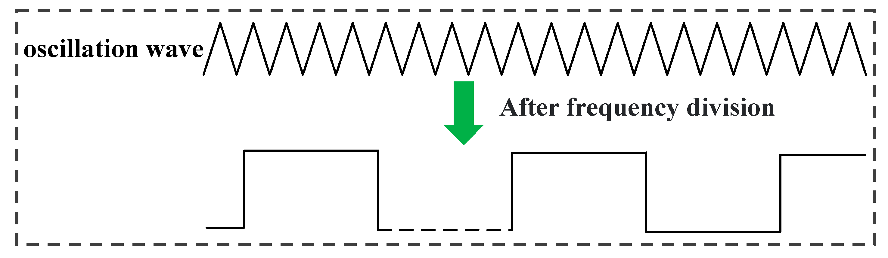
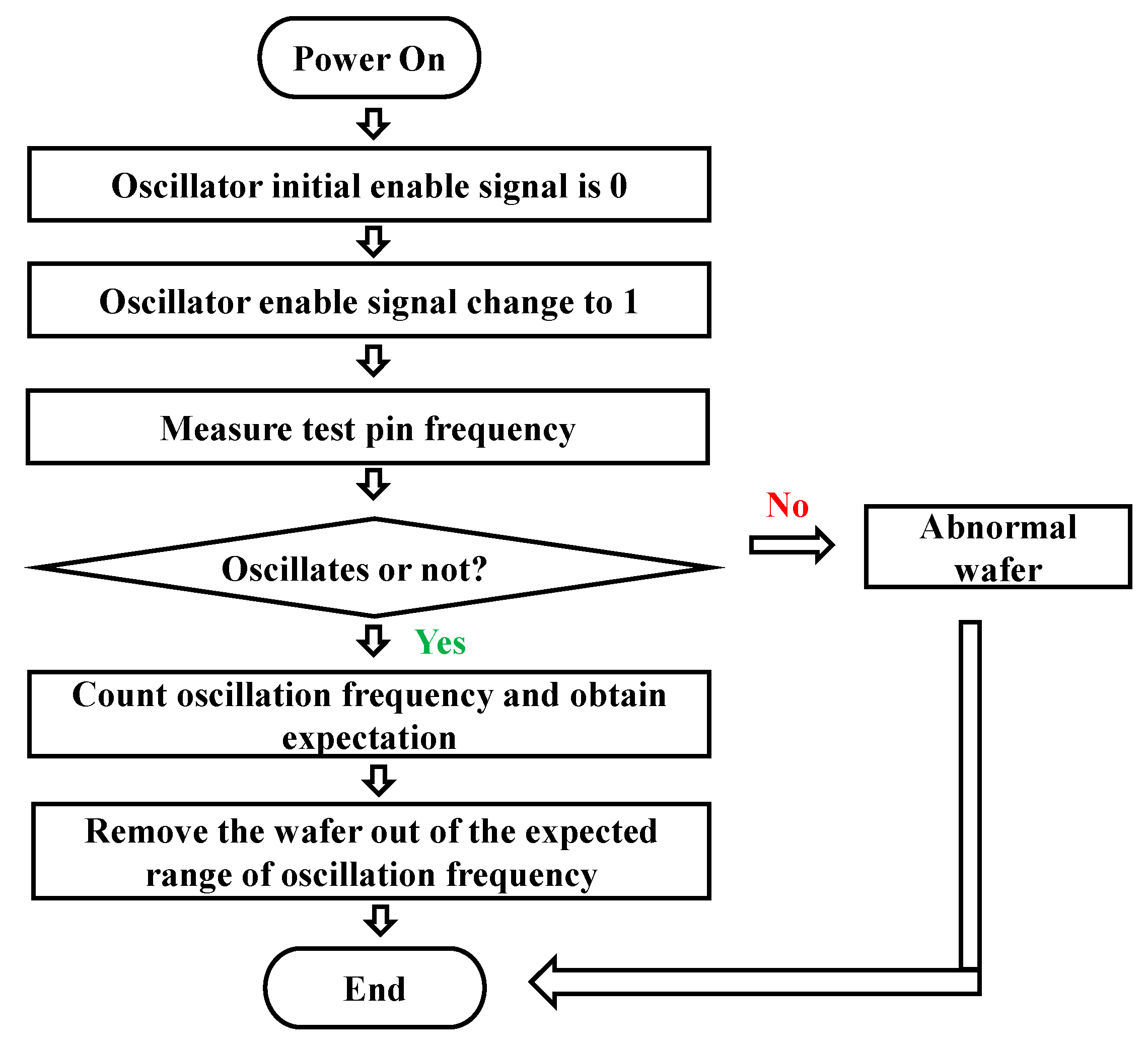
3.3. Fast Test for Hybrid Bonding Connection

This work proposed a test method for an HB ring, which makes a ring of specially tested HB around the HB of the key signal, as shown in Figure 8. There is an odd number of inverters in the ring to form an oscillation ring. The connectivity of the HB ring can be judged by measuring the out pin of the oscillation, as shown in Figure 9. Based on experience, high-risk HB in the outer ring is measured to realize the indirect test of the HB connection status of key signals after stacking. Therefore, it is not necessary to spend a lot of extra areas to make a special test circuit for HB by our proposed method to reduce the test cost.
HB and back end of line (BEOL) metal can be equivalent to two RC structures. Afterward, the two RC together with a simple inverter forms an oscillating ring. To increase the weight of HB occupying RC in the whole ring, which can better improve the accuracy of the results, the top metal of logic and the top metal of DRAM connect more HB vias in series and then pass through BEOL metal to invert at the next level. Figure 10 shows the equivalent circuit diagram.
Oscillating ring frequency is relatively high, and direct measurement puts forward higher requirements for test equipment. Therefore, a frequency divider is added to the output end of the oscillating ring to reduce the frequency of the test end and hence reduce the cost of test equipment. Figure 11 shows the schematic diagram of waveforms of the HB ring before and after frequency division.
Figure 12 shows the HB ring test flow. First, the test voltage is applied by power on. Second, an input end of an AND gate in the oscillating ring is initially pulled down to 0. Then, the previously initialized input of the AND gate in the oscillating ring starts to pull up to 1 to detect the HB connectivity state. Third, the HB connection is obtained by testing the frequency of the output pin. If there is no oscillation at the output, the HB state is considered open. Otherwise, oscillation occurs, which indicates that the connection is initially effective. Next, the normal distribution of oscillation frequency is statistically analyzed to further judge the HB connection state. The expected value is obtained by counting the oscillation frequency at the output pin. Finally, the chip out of the expected range of oscillation frequency is judged as an abnormal chip due to a failure in the HB connection.

4. Results and Discussion

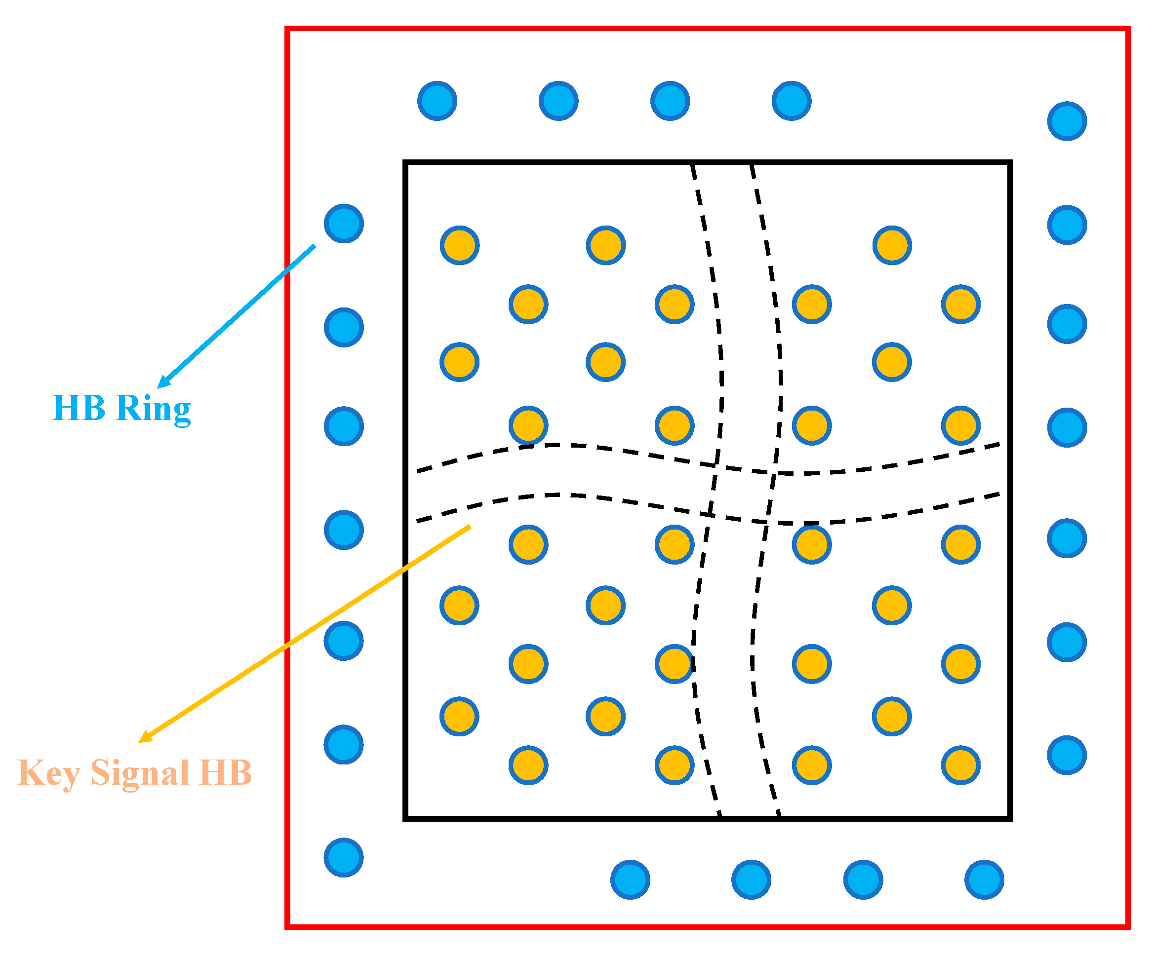
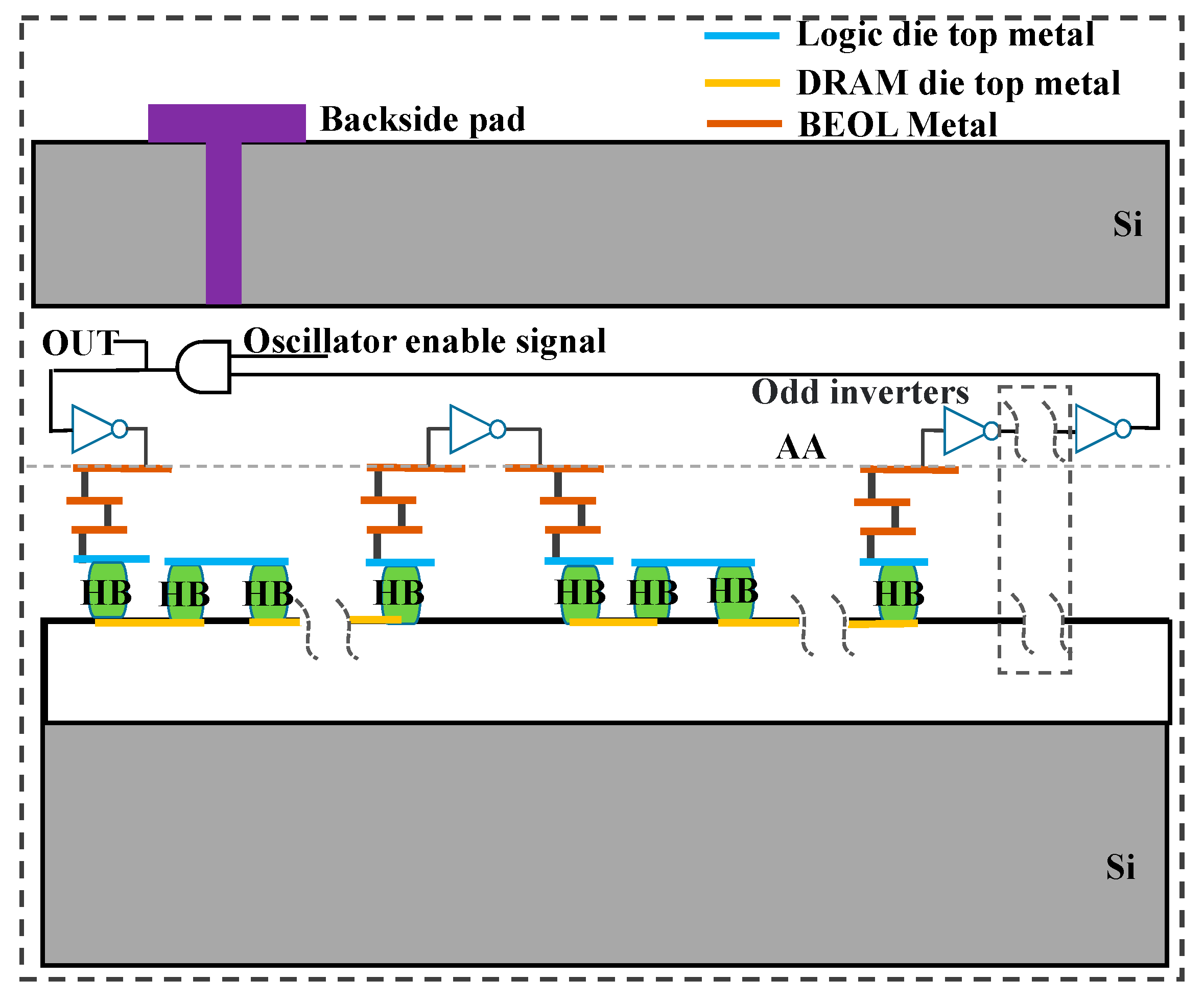
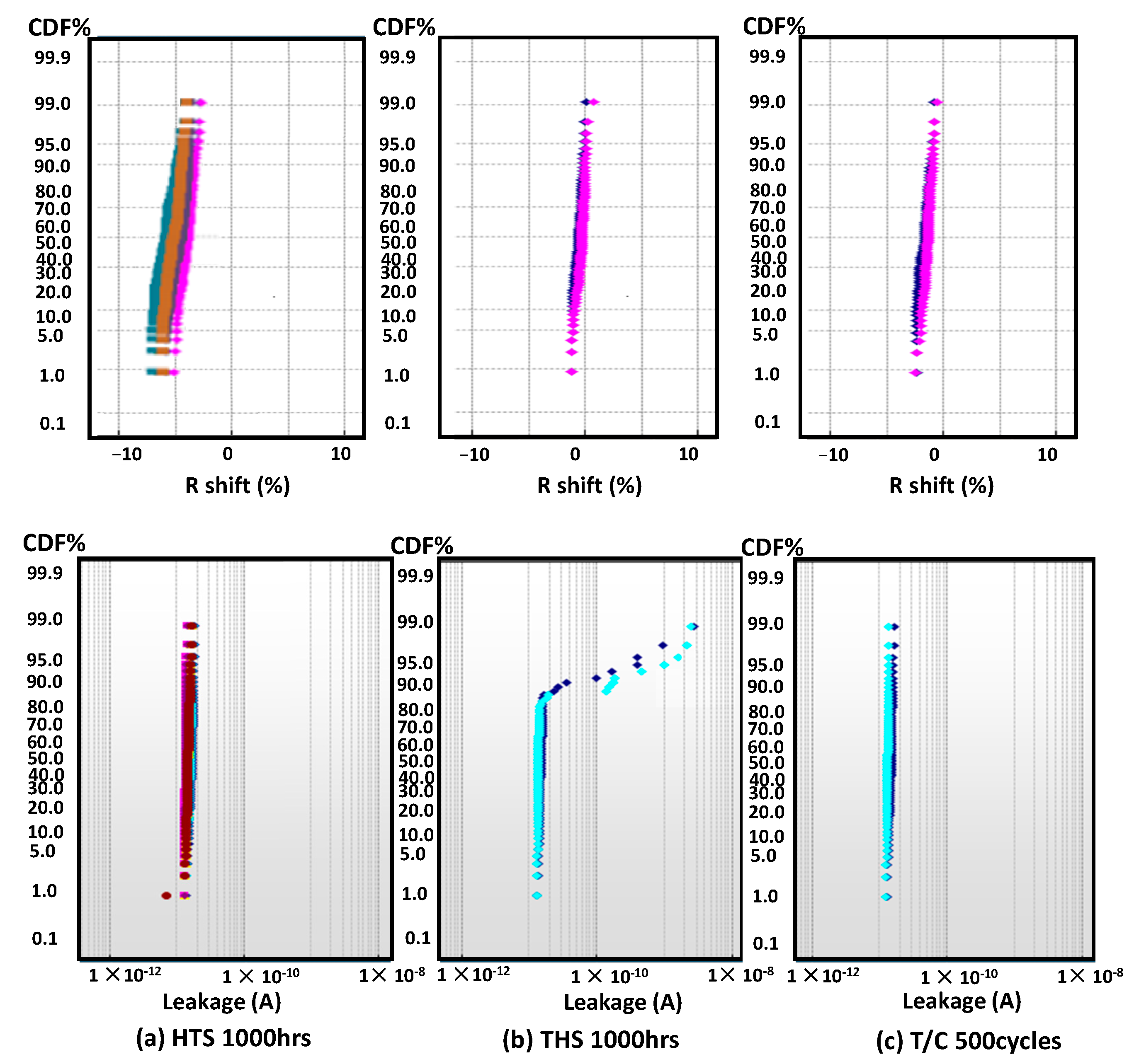
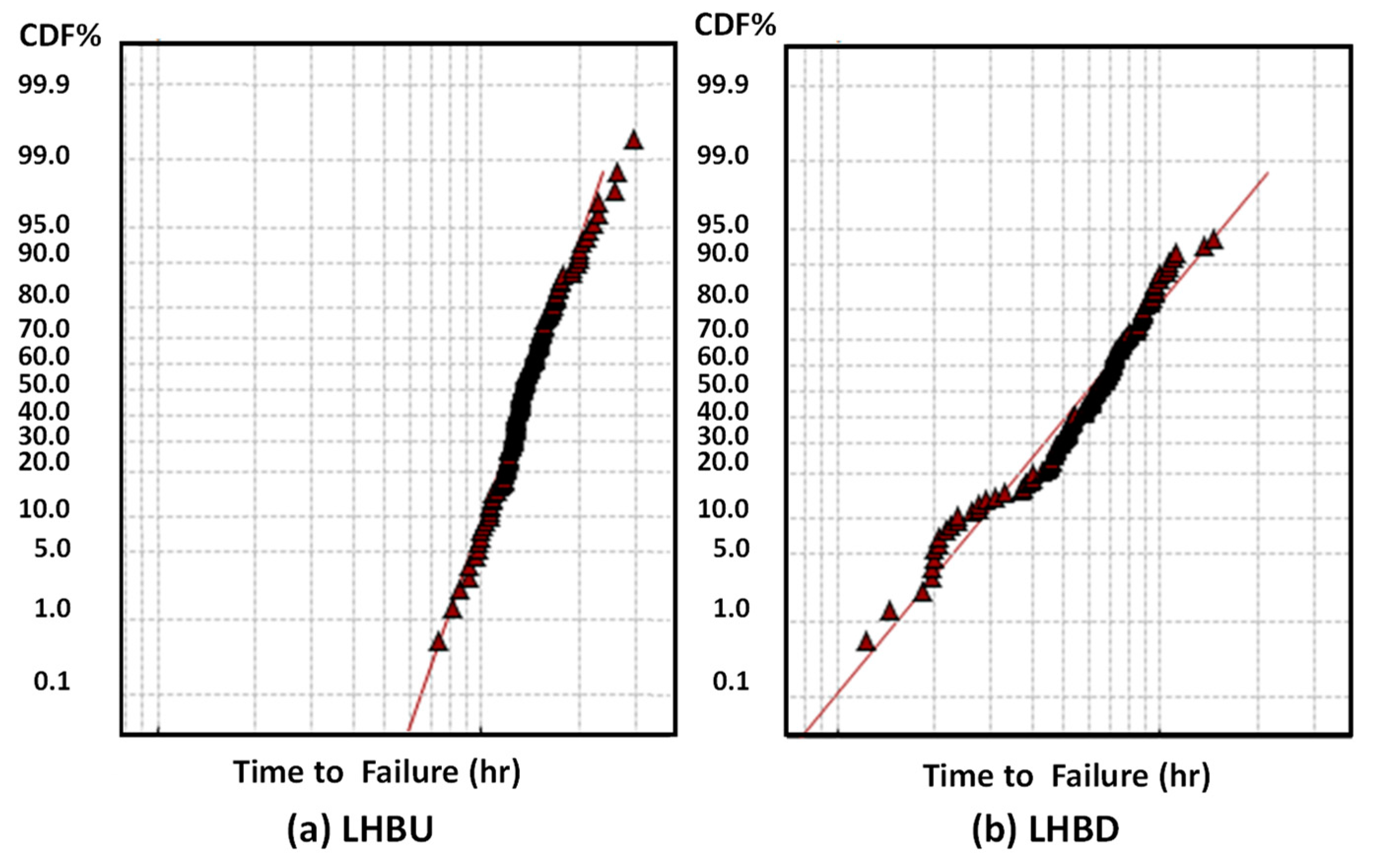
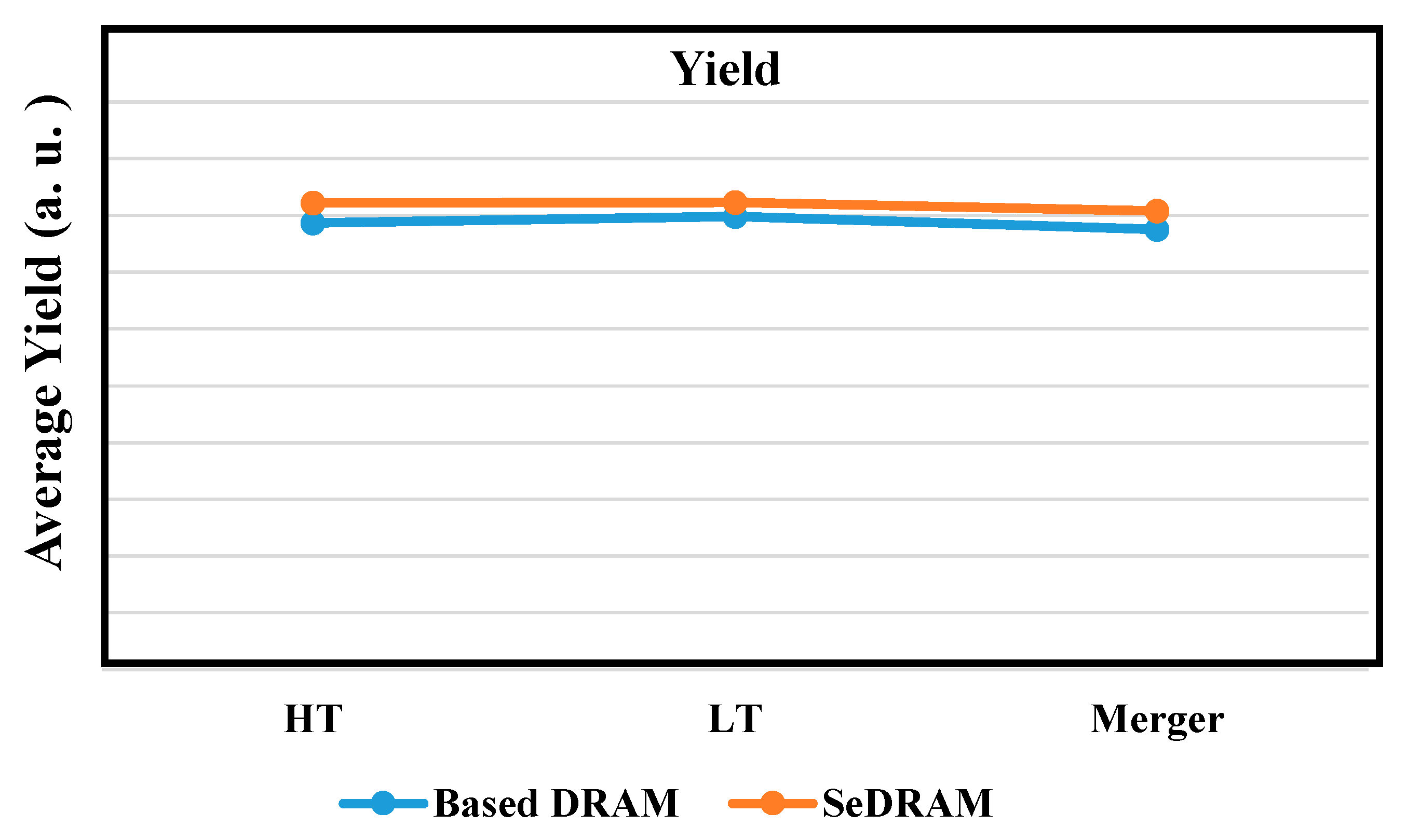
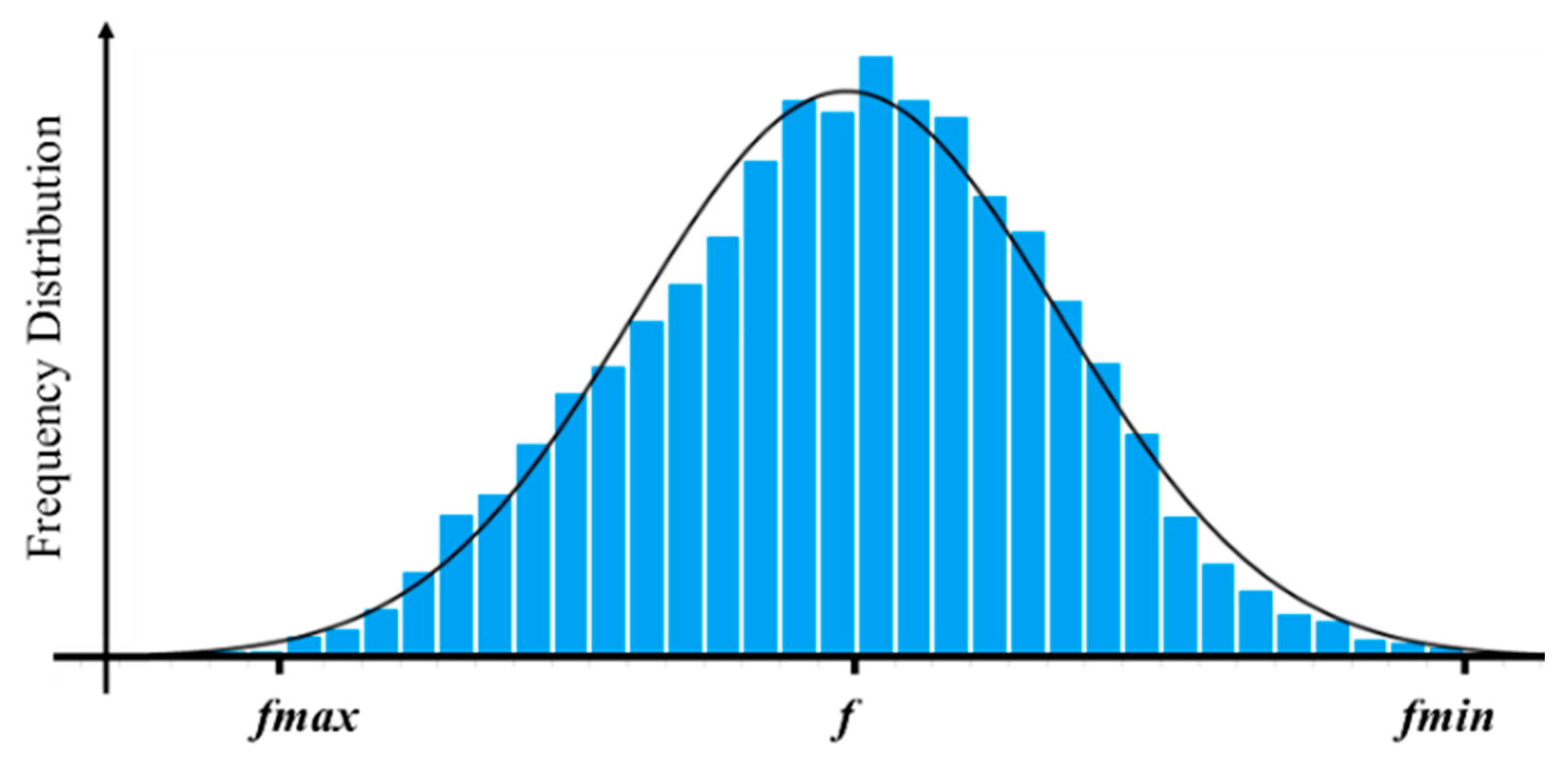
4.1. Hybrid Bonding Test-Key Results

The reliability evaluation according to JEDEC standard include temperature cycling (T/C), high temperature stress (HTS), temperature humidity stress (THS), and electro-migration (EM). Resistance and leakage degradation are evaluated after T/C, HTS, and THS, while the current tolerance of the bonding via and interface test is simulated by EM.
We directly test HB structures in test-key. Figure 13 shows the cumulative failure plot of hybrid bonding test results after reliability tests [1]. The vertical axis is the cumulative failure rate and the horizontal axis is resistance shift rate and leakage. Figure 13a shows after HTS1000hrs the maximum resistance shift was suppressed to 6.95%, and the leakage current was 18 pA at 29 V voltage bias. Therefore, it was determined that the insulation property of hybrid bonding is sufficient. Figure 13b shows the cumulative failure plot of hybrid bonding resistance shift and leakage after THS 1000 h. The humidity environment stress (85C/85%RH) was implemented in this test. The plot charts show that resistance and leakage degradation are negligibly small. The anomalous part comes from the wafer edge in Figure 13b, but the maximum results (2.79 nA) are still in the specification (10 nA). It indicates the hybrid bonding process was strong enough to encounter a humidity attack. Figure 13c shows the thermal cycle was used to evaluate the hybrid bonding structure fatigue properties. The environment temperature from −65C was raised to 150C and then cooled down to 165C, which is called 1 cycle. After 500 cycles, the max value of resistant shift is −2.52%, and leakage is on a very low level of 16.9 pA.
As hybrid bonding structure can be extracted as a BEOL via connection, the EM characterization was generally indicated as the metal migration endurance under big electric current stress. The single hybrid bonding via to logic or array wafer top metal interface, which called upstream and downstream structure were evaluated with the JEDEC standard method. Figure 14 shows the lifetime under use conditions are 2 × 10⁵ and 3.3 × 10³ years for upstream structure (LHDU: from array to logic) and downstream structure (LHBD: from logic to array), respectively. As can be expected, upstream with copper-to-copper interface has more robust EM.

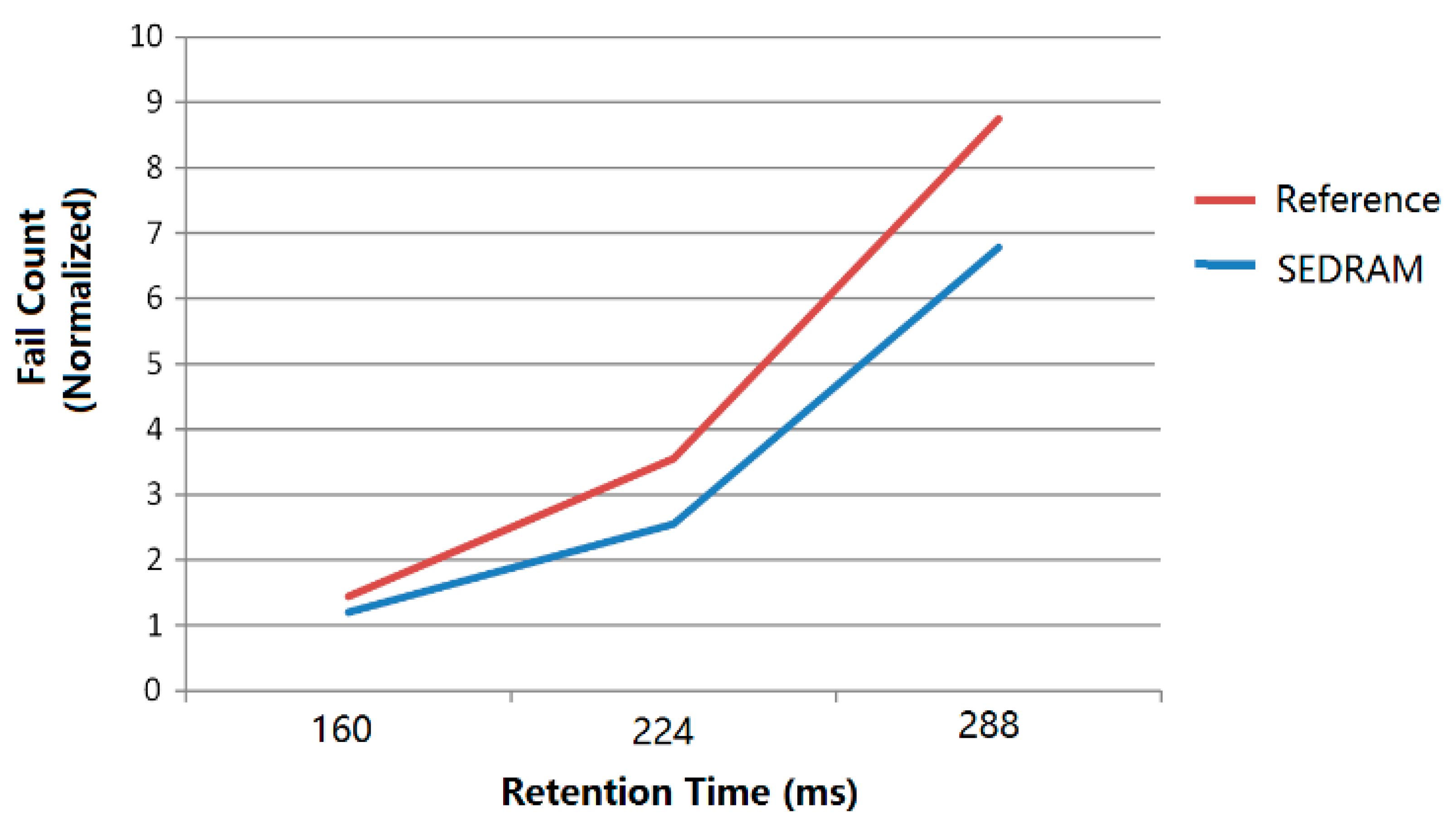
4.2. A 4 Gb LPDDR4/4X by SeDRAM Test Results

A 4 Gb LPDDR4/4X product based on SeDRAM technology is fabricated to verify the toggling speed and potential risk related to HB flow. The SeDRAM chip photograph is shown in Figure 15a, which compatible complying with the standard LPDDR4/4X specification. Figure 15b,c show the two overlay die layout, where the array die consists of four identical 1 Gbit dies fabricated in a 25 nm three-metal DRAM process, and the logic die includes two mirrored channel structure dies using a 55 nm seven-metal logic process. In total, the chip was 4 Gbit LPDDR4/4X and the 66.3 mm2 die size included more than 64K HB vias per chip.
The shmoo test is a common technical means in chip testing. The method is to select two indicators related to chip performance (e.g., SeDRAM access time) and then scan the two indicators (e.g., strobe location and main clock cycle) in two dimensions separately and display the scanning results in the two-dimensional coordinate system of X-Y. The SeDRAM access time shmoo plot result is shown in Figure 16. The shmoo in Figure 16 is used for evaluating the access speed. The horizontal axis is the strobe location and the vertical axis is main clock cycle. Figure 16a,b show the minimum tCK of two channels can reach 0.56 ns, which is beyond the limit of the frequency of testor. The DRAM components passed 4266 Mbps for speed bin sorting in multiple cases, including high temperature (95C), high voltage (VDD1 = 1.2 v, VDD1 = 2 v), and low voltage (VDD2 = 1.05 v, VDD1 = 1.65 v). Considering 16 pre-fetches of LPDDR4/4X, the 266 MHz data rate of HB interface can be represented by the 4266 Mbps test results.
SeDRAM relies on a wafer-on-wafer stacking structure [21]. In the stacked chip, the measured logic wafer thickness is just 3 µm, compared with 750 µm of array wafer thickness. The thinned logic wafer and the abundant HB vias can lower the interconnection thermal resistance and help heat dissipation. Moreover, because the logic-to-DRAM interface frequency of SeDRAM is as low as 266 MHz, the SeDRAM consumes less power than HBM and achieves power efficiency. We have measured the IDD4 of our proposed LPDDR4/4X for power consumption estimation. IDD currents (such as IDD4W, IDD4R) are measured as time-averaged currents with all VDD balls of the SeDRAM being tested tied together. IDD4W and IDD4R reflect the operating burst write current and read current according to the JEDEC, which stands for power consumption during high-bandwidth operation. During the IDD4W/R test, the VDD2 (1.2 v) andVDD1 (2 v) for SeDRAM with a data rate of 4266 Mbps and data I/O of 4096 under room temperature achieve 0.88 pJ/b and 0.49 pJ/b, respectively. Even in the worst case, the power efficiency of our proposed SeDRAM is as low as 0.88 pJ/b. Compared to HBM3, the major competitor for high-bandwidth memory, the SeDRAM energy efficiency is reduced by 70%, as shown in Figure 17. The benchmark Table 1 below compares the major competitors in high bandwidth memory (e.g., GDDR6 and HBM).
Finally, the thermal challenge is well managed in SeDRAM. As shown in Figure 18, the horizontal axis is the cell retention time and the vertical axis is normalized fail count, and the retention time of SeDRAM is equivalent to a reference conventional DRAM process. LPDDR4/4X chip from the conventional DRAM process and meets the design target of 96 ms at 95 °C.

4.3. Hybrid Bonding Connection Test Results

Both indirect and direct tests are implemented in HB tests and consistently show that the HB process is stable and can be extended to commercial products successfully.
Yield analysis is used as an indirect test of HB. Due to the establishment of robust HB connectivity and stable back end metallization process, the final DRAM product evaluation results showed no reduction in yield compared to mass-produced existing DRAM products. Moreover, because periphery circuits are moved to the logic die, the SeDRAM is less area and suffers less manufacture defects, even achieving higher yield than baseline DRAM, as shown in Figure 19. The test conditions include high temperature, low temperature, and merger. This proves that even when HB processes are added to the DRAM production process, the SeDRAM can be mass-produced without affecting the characteristics of existing DRAM.
Additionally, to quickly check the quality of HB, we tested the HB ring surrounding the key HB to directly monitor the overall quality of HB.
The HB structure can be considered as an equivalent BEOL via connection; the reliability of HB is proven by the test results in Section 4.1. However, there are more than 16K HB vias per 1 Gb in total. The failure rate will definitely accumulate when the total SeDRAM density increases. Dedicated test procedures are designed to screen out failed HB structures to guarantee connection integrity. The detection of connectivity after chip stacking is implemented efficiently by our proposal to save the overall test.
We measure the frequency of the oscillator from a dedicated test pin. If there is no oscillation, the oscillator ring is open, and the logic-to-DRAM interface is defective in the current chip. Otherwise, oscillation occurs, and it indicates that the connection is effective and the oscillation frequency (f) is measured. Actually, a ring oscillator is commonly used to statistically monitor the process variation in mass production. Figure 20 shows the frequency distribution of good chips. Thanks to the robust HB connectivity and stable backend metallization process setup, the SeDRAM product is stable in a mass product.

5. Conclusions

In this work, we demonstrate a new SeDRAM with HB suitable for high bandwidth DRAM with high energy efficiency. We discussed the main key factors during the SeDRAM design to provide guidance and added new DFT features (e.g., test for fast HB rings with a low-cost). We fabricated an LPDD4/4X product with the SeDRAM, with 1024 I/O of 266 MHz providing a bandwidth of 34 GBps and power efficiency of 0.88 pJ/bit. The SeDRAM solution can also support a wide density range of 1 G/2 G/3 G/4 G/6 G/8 G/12 G/24 G/36 G/48 Gbit and a bandwidth of TBps. 3D-stacking technology using hybrid bonding enables DRAM devices with higher bandwidths to break through the memory wall. Moreover, the logic layers in the SeDRAM offer interesting possibilities for near-memory computing/computing-in-memory and sophisticated memory controller functionality.

Author Contributions

Conceptualization, S.W. and X.J.; Funding acquisition, Y.K.; Investigation, S.W., X.J., F.B. and W.X.; Methodology, S.W., F.B. and W.X.; Project administration, S.W.; Software, X.L.; Supervision, Y.K.; Validation, F.B. and X.L.; Writing—original draft, S.W., F.B. and W.X.; Writing—review & editing, X.J., Q.R. and Y.K. All authors have read and agreed to the published version of the manuscript.

Funding

This research was funded by the National Key R&D Program of China under grant No. 2019YFB2204800.

Institutional Review Board Statement

Not applicable.

Informed Consent Statement

Not applicable.

Data Availability Statement

Data are available upon request from authors.

Conflicts of Interest

The authors declare no conflict of interest.

References

  1. Bai, F.J.; Jiang, X.P.; Wang, S.; Yu, B.; Tan, J.; Zuo, F.G.; Wang, C.J.; Wang, F.; Long, X.D.; Yu, G.Q.; et al. A stacked embedded DRAM array for LPDDR4/4X using hybrid bonding 3D integration with 34GB/s/1Gb 0.88 pJ/b logic-to-memory interface. In Proceedings of the 2020 IEEE International Electron Devices Meeting (IEDM), San Francisco, CA, USA, 12–18 December 2020; pp. 6.6.1–6.6.4. [Google Scholar]
  2. Park, S.K. Technology scaling challenge and future prospects of DRAM and NAND flash memory. In Proceedings of the 2015 IEEE International Memory Workshop (IMW), Monterey, CA, USA, 17–20 May 2015; pp. 1–4. [Google Scholar]
  3. Kwon, Y.C.; Lee, S.H.; Lee, J.; Kwon, S.H.; Ryu, J.M.; Son, J.P.; Seongil, O.; Yu, H.-S.; Lee, H.; Kim, S.Y.; et al. A 20nm 6GB function-in-memory DRAM, based on HBM2 with a 1.2 TFLOPS programmable computing unit using bank-level parallelism, for machine learning applications. In Proceedings of the 2021 IEEE International Solid- State Circuits Conference (ISSCC), San Francisco, CA, USA, 13–22 February 2021; pp. 350–352. [Google Scholar]
  4. Niu, D.M.; Li, S.C.; Wang, Y.H.; Han, W.; Zhang, Z.; Guan, Y.J.; Guan, T.C.; Sun, F.; Xue, F.; Duan, L.D.; et al. 184QPS/W 64Mb/mm23D logic-to-DRAM hybrid bonding with process-near-memory engine for recommendation system. In Proceedings of the 2022 IEEE International Solid-State Circuits Conference (ISSCC), San Francisco, CA, USA, 20–26 February 2022; pp. 1–3. [Google Scholar]
  5. Hwang, K.-D.; Kim, B.; Byeon, S.-Y.; Kim, K.-Y.; Kwon, D.-H.; Lee, H.-B.; Lee, G.-I.; Yoon, S.-S.; Cha, J.-Y.; Jang, S.-Y.; et al. A 16Gb/s/pin 8Gb GDDR6 DRAM with bandwidth extension techniques for high-speed applications. In Proceedings of the 2018 IEEE International Solid-State Circuits Conference (ISSCC), San Francisco, CA, USA, 11–15 February 2018; pp. 210–212. [Google Scholar]
  6. Hollis, T.M.; Schneider, R.; Brox, M.; Hein, T.; Spirkl, W.; Bach, M.; Balakrishnan, M.; Funfrock, F.; Ivanov, M.; Jovanovic, N.; et al. An 8-Gb GDDR6X DRAM achieving 22 Gb/s/pin With Single-Ended PAM-4 Signaling. IEEE J. Solid-State Circuits 2021, 57, 224–235. [Google Scholar] [CrossRef]
  7. O’Connor, M.; Chatterjee, N.; Lee, D.; Wilson, J.; Agrawal, A.; Keckler, S.W.; Dally, W.J. Fine-grained DRAM: Energy-efficient DRAM for extreme bandwidth systems. In Proceedings of the 50th Annual IEEE/ACM International Symposium on Microarchitecture, Boston, MA, USA, 14–17 October 2017; pp. 41–54. [Google Scholar]
  8. Jun, H.; Cho, J.; Lee, K.; Son, H.Y.; Kim, K.; Jin, H.; Kim, K. HBM (high bandwidth memory) DRAM technology and architecture. In Proceedings of the 2017 IEEE International Memory Workshop (IMW), Monterey, CA, USA, 14–17 May 2017; pp. 1–4. [Google Scholar]
  9. Park, M.-J.; Cho, H.S.; Yun, T.-S.; Byeon, S.; Koo, Y.J.; Yoon, S.; Lee, D.U.; Choi, S.; Park, J.; Lee, J.; et al. A 192-Gb 12-high 896-Gb/s HBM3 DRAM with a TSV auto-calibration scheme and machine-learning-based layout optimization. In Proceedings of the 2022 IEEE International Solid- State Circuits Conference (ISSCC), San Francisco, CA, USA, 20–26 February 2022; pp. 444–446. [Google Scholar]
  10. Chujo, N.; Sakui, K.; Ryoson, H.; Sugatani, S.; Nakamura, T.; Ohba, T. Bumpless build cube (BBCube): High-parallelism, high-heat-dissipation and low-power stacked memory using wafer-level 3D integration Process. In Proceedings of the 2020 IEEE Symposium on VLSI Technology, Honolulu, HI, USA, 16–19 June 2020; pp. 1–2. [Google Scholar]
  11. Michailos, J.; Coudrain, P.; Farcy, A.; Hotellier, N.; Cheramy, S.; Lhostis, S.; Deloffre, E.; Sanchez, Y.; Jouve, A.; Guyader, F.; et al. New challenges and opportunities for 3D integrations. In Proceedings of the 2015 IEEE International Electron Devices Meeting (IEDM), Washington, DC, USA, 7–9 December 2015; pp. 8.5.1–8.5.4. [Google Scholar]
  12. Tsai, Y.C.; Lee, C.H.; Chang, H.C.; Liu, J.H.; Hu, H.W.; Ito, H.; Kim, Y.S.; Ohba, T.; Chen, K.-N. Electrical characteristics and reliability of wafer-on-wafer (WOW) bumpless through-silicon via. IEEE Trans. Electron Devices 2021, 68, 3520–3525. [Google Scholar] [CrossRef]
  13. Sakui, K.; Ohba, T. High bandwidth memory (HBM) and high bandwidth NAND (HBN) with the bumpless TSV technology. In Proceedings of the International 3D Systems Integration Conference (3DIC), Sendai, Japan, 8–10 October 2019; pp. 1–4. [Google Scholar]
  14. Kim, Y.S.; Kodama, S.; Maeda, N.; Fujimoto, K.; Mizushima, Y.; Kawai, A.; Hsu, T.C.; Tzeng, P.; Ku, T.K.; Ohba, T. Electrical characteristics of bumpless interconnects for through silicon via (TSV) and wafer-on-wafer (WOW) integration. In Proceedings of the International Conference on Electronics Packaging (ICEP), Hokkaido, Japan, 20–22 April 2016; pp. 74–78. [Google Scholar]
  15. Kim, S.H.; Kang, P.; Kim, T.; Lee, K.; Jang, J.; Moon, K.; Na, H.; Hyun, S.; Hwang, K. Cu microstructure of high density Cu hybrid bonding interconnection. In Proceedings of the IEEE 69th Electronic Components and Technology Conference (ECTC), Las Vegas, NV, USA, 28–31 May 2019; pp. 636–641. [Google Scholar]
  16. Lee, D.U.; Kim, K.W.; Kim, K.W.; Kim, H.; Kim, J.Y.; Park, Y.J.; Kim, J.H.; Kim, D.S.; Park, H.B.; Shin, J.W.; et al. A 1.2V 8Gb 8-channel 128GB/s high-bandwidth memory (HBM) stacked DRAM with effective microbump I/O test methods using 29nm process and TSV. In Proceedings of the 2014 IEEE International Solid- State Circuits Conference (ISSCC), San Francisco, CA, USA, 9–13 February 2014; pp. 432–433. [Google Scholar]
  17. Jiang, X.P.; Zuo, F.G.; Wang, S.; Zhou, X.F.; Wang, Y.B.; Liu, Q.; Ren, Q.W.; Liu, M. A 1596-GB/s 48-Gb stacked embedded DRAM 384-Core SoC with hybrid bonding integration. IEEE Solid-State Circuits Lett. 2022, 5, 110–113. [Google Scholar] [CrossRef]
  18. Jiang, X.P.; Zuo, F.G.; Wang, S.; Zhou, X.F.; Yu, B.; Wang, Y.B.; Liu, Q.; Liu, M.; Kang, Y.; Ren, Q.W. A 1596GB/s 48Gb embedded DRAM 384-Core SoC with hybrid bonding integration. In Proceedings of the 2021 IEEE Asian Solid-State Circuits Conference (A-SSCC), Busan, Republic of Korea, 7–10 November 2021; pp. 1–3. [Google Scholar]
  19. Li, Y.; Schneider, H.; Schnabel, F.; Thewes, R.; Schmitt-Landsiedel, D. DRAM yield analysis and optimization by a statistical design approach. IEEE Trans. Circuits Syst. I Regul. Pap. 2011, 58, 2906–2918. [Google Scholar] [CrossRef]
  20. Van De Goor, A.J.; Schanstra, I. Address and data scrambling: Causes and impact on memory tests. In Proceedings of the First IEEE International Workshop on Electronic Design, Test and Applications, Christchurch, New Zealand, 29–31 January 2002; pp. 1–9. [Google Scholar]
  21. Park, J.; Lee, B.; Lee, H.; Lim, D.; Kang, J.; Cho, C.; Na, M.; Jin, I. Wafer to wafer hybrid bonding for DRAM applications. In Proceedings of the 2022 IEEE 72nd Electronic Components and Technology Conference (ECTC), San Diego, CA, USA, 31 May 2022–3 June 2022; pp. 126–129. [Google Scholar]
  22. Lee, D.U.; Cho, H.S.; Kim, J.; Ku, Y.J.; Oh, S.; Kim, C.D.; Kim, H.W.; Lee, W.Y.; Kim, T.K.; Yun, T.S.; et al. A 128Gb 8-High 512GB/s HBM2E DRAM with a Pseudo Quarter Bank Structure, Power Dispersion and an Instruction-Based At-Speed PMBIST. In Proceedings of the 2020 IEEE International Solid- State Circuits Conference (ISSCC), San Francisco, CA, USA, 16–20 February 2020; pp. 334–336. [Google Scholar]
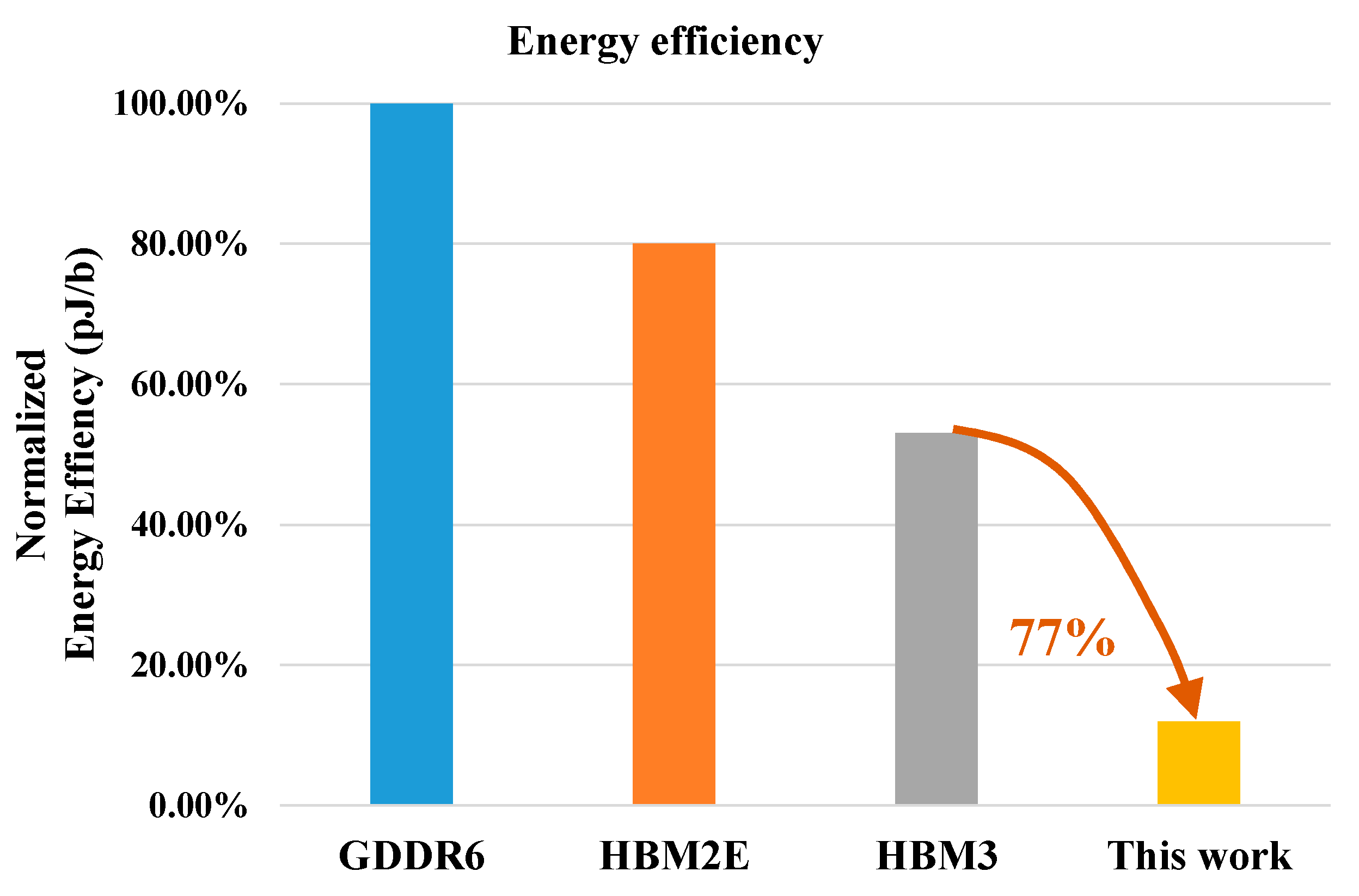
Figure 1. Structure of the proposed SeDRAM.
Electronics 12 01077 g001
Figure 2. Hybrid bonding process flow of our proposed SeDRAM.
Electronics 12 01077 g002
Figure 3. SeDRAM cross-sectional TEM image. The logic wafer (top) and array wafer (bottom) are bonded face to face via hybrid bonding. The dotted lines are the interface between two wafers.
Electronics 12 01077 g003
Figure 4. (a) Logic die and (b) array die of 36 Gb SeDRAM. The logic die is a 3 × 3 mesh network-on-chip (NoC) with 55 nm technology, and the array die consists of 6 × 6 memory units.
Electronics 12 01077 g004
Figure 5. Logic-to-DRAM interface of SeDRAM.
Electronics 12 01077 g005
Figure 6. (a) Write and (b) read timing diagram of SeDRAM.
Electronics 12 01077 g006
Figure 7. Interface between logic die and array die of SeDRAM.
Electronics 12 01077 g007
Figure 8. Hybrid bonding (HB) ring top view diagram.
Electronics 12 01077 g008
Figure 9. Hybrid bonding ring test structure profile.
Electronics 12 01077 g009
Figure 10. Hybrid bonding ring circuit schematic.
Electronics 12 01077 g010
Figure 11. Schematic diagram of waveforms of hybrid bonding ring before and after frequency division.
Electronics 12 01077 g011
Figure 12. Hybrid bonding ring test flow.
Electronics 12 01077 g012
Figure 13. Hybrid bonding reliability test results after (a) high temperature stress (HTS) 1000 hrs, (b) temperature humidity stress (THS) 1000 hrs, and (c) thermal cycle (T/C) 500 cycles, where different color curves represent data from different wafers and different test structures.
Electronics 12 01077 g013
Figure 14. Hybrid bonding EM test results of (a) HLBU (large hybrid bond upstream) and (b) HLBD (large hybrid bond downstream), where hybrid bonding vias to logic/array wafer top metal interface were called upstream/downstream, respectively.
Electronics 12 01077 g014
Figure 15. (a) Wafer photograph, (b) array die layout, and (c) logic die layout of LPDDR4/4X based on SeDRAM. DRAM and logic wafer were bonded face to face by hybrid bonding. DRAM die on DRAM wafer consists of 4 dies with 1 Gbit. Logic die on logic wafer supports 2-channel (A and B) LPDDR4 interface.
Electronics 12 01077 g015
Figure 16. SeDRAM Access time shmoo result of (a) channel A and (b) channel B.
Electronics 12 01077 g016
Figure 17. Energy efficiency comparison.
Electronics 12 01077 g017
Figure 18. SeDRAM retention time result.
Electronics 12 01077 g018
Figure 19. Comparison of yield between based DRAM and SeDRAM.
Electronics 12 01077 g019
Figure 20. Ring oscillation frequency distribution.
Electronics 12 01077 g020
Table 1. Summary of high-bandwidth memories.
GDDR6
ISSCC2018
[5]
HBM2E
ISSCC2020
[22]
HBM3
ISSCC2022
[9]
This Work
Connection-ubumpubumpHybrid bonding
PHY-YesYesNo
IO32102410244096
Speed (Mbps)16,38440967168266
Total Bandwidth (GBps)64512896136
Density (Gbit)81281924
Energy Efficiency (a. u)100%80%53%12%
Bandwidth per Gbit (GBps/Gbit)844.734
Disclaimer/Publisher’s Note: The statements, opinions and data contained in all publications are solely those of the individual author(s) and contributor(s) and not of MDPI and/or the editor(s). MDPI and/or the editor(s) disclaim responsibility for any injury to people or property resulting from any ideas, methods, instructions or products referred to in the content.

