Article

Evaluating Cu Printed Interconnects “Sinterconnects” versus Wire Bonds for Switching Converters

Silicon Austria Labs GmbH, Europastrasse 12, 9524 Villach, Austria
*
Author to whom correspondence should be addressed.
Electronics 2022, 11(9), 1373; https://doi.org/10.3390/electronics11091373
Submission received: 21 March 2022 / Revised: 8 April 2022 / Accepted: 19 April 2022 / Published: 25 April 2022
(This article belongs to the Special Issue Interconnects for Electronics Packaging)

Abstract

:
This paper demonstrates the feasibility of the printed copper (Cu) paste interconnects for applications in power semiconductor modules and switching converters. Copper sinter paste interconnects denoted as “Sinterconnects” have been recently introduced as an alternative to wire-bonding technology for power electronic device packaging. However, the electrical domain properties of these novel interconnects have not yet been investigated in detail. To address this research opportunity, this paper evaluates the performance of two different types of Sinterconnects applied to multi-chip, insulated gate bipolar transistor (IGBT) power modules. First, parasitic or stray inductances of these Sinterconnected systems are calculated analytically and by using three-dimensional finite element (FE) analysis. In addition to that, resistivity ( ρ ) of those has been analysed and compared with conventional wire bond technology. Finally, the performances of the Sinterconnects in power device assemblies are experimentally investigated. Two Sinterconnect structures (i.e., printed Cu paste and Cu clip attach) as well as a state-of-the-art wire-bonded IGBT module, have been integrated into a switching DC-DC converter and benchmarked. Experimental measurements show how converters with Sinterconnects enable efficient power conversion.

1. Introduction

Aluminum (Al) wire bonding technology is used for power module packaging due to its low cost, good bonding ability, good electrical conductivity and reliability to some extent. However, as power rating increases, Al bonding wire cannot meet the electrical requirement. For instance, a single Al wire with a diameter of 500 μ m can carry 10 A at maximum [1]. In order to increase the current carrying capability, which is a must for high power IGBT modules, several Al wire bonds must be arranged in parallel [2].
Unfortunately, due to paralleling the reliability and low-cost features of the power module could be compromised. Moreover, the capacitive and inductive coupling resulting from the Al wire interconnects between the semiconductor pads and package can introduce several issues. Additionally, results of paralleling include electrical isolation failures, increased noise and cross-talk, and, in general, reduced performance [3,4,5,6,7]. Bond wires are a major source of parasitic circuit elements, and researchers have shown that one of the main reasons for power semiconductor failure is due to parasitic effects. In [8], Stefan et al. show how the stray inductance has an impact on switching losses. Eckart et al., in [9], presented the effects of parasitic in semiconductor properties, package and switching cell design. In [10], it has been reported that the main reason for IGBT failure is due to the breakage and shedding of the bond wire. The failure mechanism of bond wire lift-off is exacerbated by the mismatch of the coefficient of thermal expansion (CTE) between silicon (Si) and Al. In [11], E. Deng et al. explain that, due to difference in CTE between silicon (3 ppm/ ° C) and aluminium (22 ppm/ ° C), thermal stress could cause some crack in the solder layer. T. Polom et al. in [12] reported a method, using modeling and simulation, to identify temperature gradients specific to a power electronic package. The spatial thermal impedances were investigated to show how the overall geometric topology of a power module can expedite lifetime consumption. The metric can also be used in parametric studies examining impacts of material composition and interconnects, topics of this paper.
As an alternative to Al, Copper can be used for bonding semiconductor modules. Cu has superior electrical and thermal conductivity as compared to Al. Also, the CTE of Cu is much closer to silicon compared to the Al. To overcome the limitation of Al wire bonding, researchers have proposed Cu wire bonds, Cu clips, power overlay structures, a flex circuit sintered on top or double side sintered direct-bonded Cu (DBC)-substrate and planar interconnect [13,14,15,16,17,18,19]. As of today, Cu wire bonds still could not find the way to the mainstream to replace Al wire bonds due to several reasons [13,14]:
(a)
Cu wires are harder than Al to bond
(b)
The higher hardness of Cu wire requires higher bond forces and ultrasonic energy. This means higher mechanical stresses to the components
(c)
The high tendency of Cu wires to oxidize results in the formation of oxide layers on its surface preventing the formation of round free-air balls
(d)
The higher cost (protective atmosphere) and lower yield
Correspondingly, more attention has been directed towards alternatives, namely wire-bondless Cu-based interconnects. Recent development in this area based on Cu clips, Cu ribbons, Cu pins, thin-film Cu, and thick Cu layer are reported in [20,21,22]. In [20], it has been shown that Cu clip technology could achieve more power density by having higher heat removal capacity from semiconductors. In addition to that, Skin [23] and SiPLIT [7] technologies have been proposed by industries. All of those innovative ideas have some advantages and disadvantages. For instance, Cu clips use solders as the clip-attach to the dies. This limits the working temperature to 200 ° C and may also introduce reliability issues. SiPLIT and Skin require lithography processes that incur complexity and extra costs.
A recent invention in this area of research uses printed Cu paste (“Sinterconnects”) instead of solder paste for attaching Cu clips to a DBC substrate. Furthermore, another type of Sinterconnects was introduced by our group, in which the clip was substituted with a fully printed Cu paste [24]. It is noteworthy to mention that since the interconnects are made via sintering of the Cu paste materials, the term “Sinterconnects” were proposed to distinguish them from conventional interconnects. So far, the electrical performance of Sinterconnects has not been analyzed and measured in detail. Furthermore, Sinterconnects have not been evaluated in the context of their envisioned end- application: switch-mode power electronic converters.
In this paper, the two versions of Sinterconnects (fully printed Cu and printed Cu clip attach) have been analyzed and compared to a state-of-the-art, wire-bond packaging solution. The paper is organized as follows. Section 2 explains the types of power semiconductor device interconnects that have been considered for this research. Section 3 presents the results of this research which includes a comparative analysis of the parasitic inductances originating from different power device interconnection systems, resistivity of the interconnects and system level performance of the different interconnect devices. Finally, Section 4 summarizes the conclusions.

2. Overview of the Candidate Interconnects
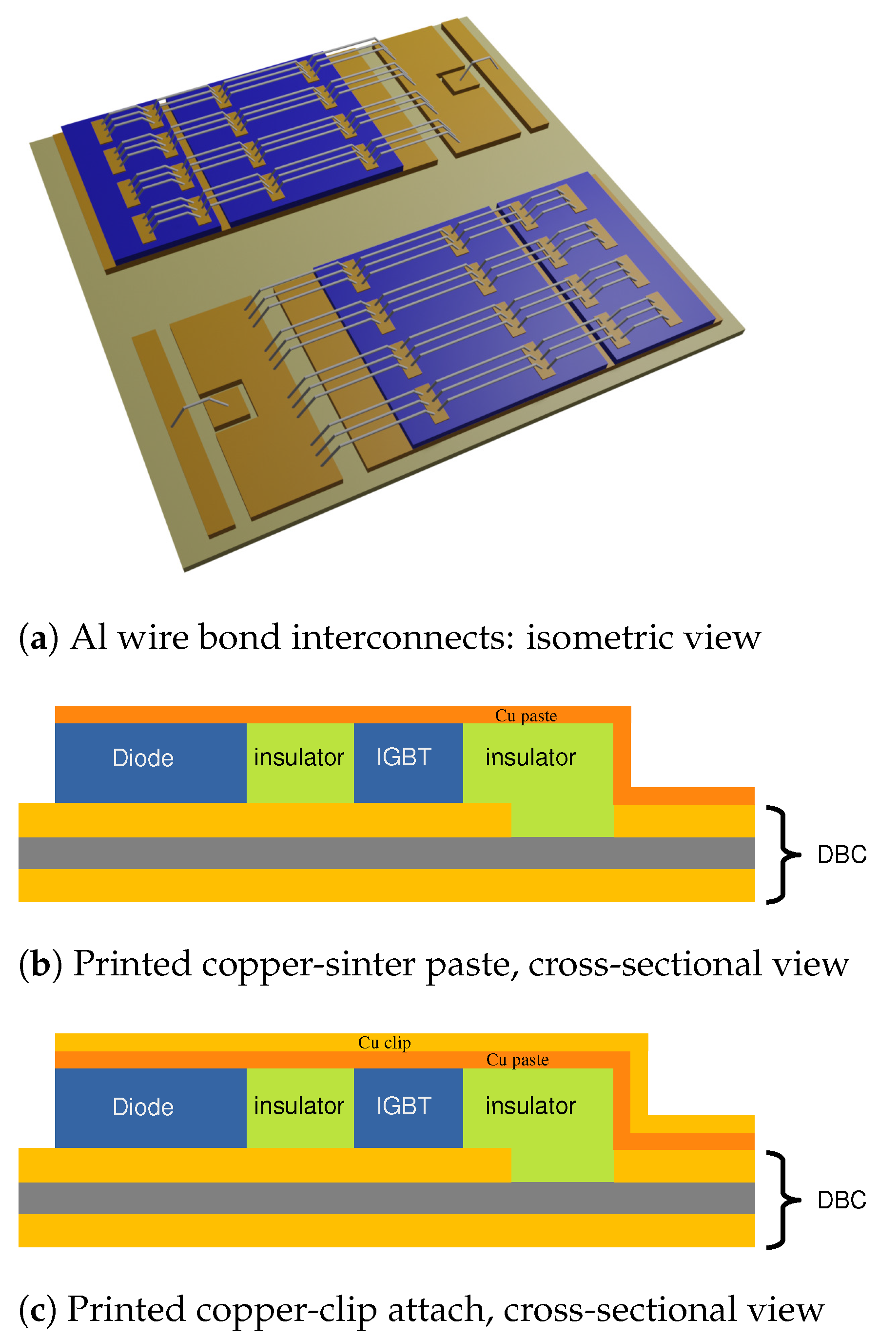
Top-side interconnects, multi-chip IGBTs have been considered for this research to carry out the experimental evaluation. The IGBT and the diode dies were already soldered on the DBC substrates. The three different structures that have been considered for front-side interconnects are as follows.

2.1. Wire Bond

The interconnects among IGBT, diode device, and DBC have been established with 12 thick Al wires each with a diameter of 300 μ m via wedge-wedge bonding.

2.2. Sinterconnect “Printed Cu”

Micron-sized Cu sinter paste was jet-printed in a drop-on-demand mode by using a modular micro-assembly station. The thickness of the Cu paste was varied in the range of 125 μ m to 300 μ m depending on printing parameters (resolution and speed).

2.3. Sinterconnect “Clip-Attach”

In this case, the Cu paste was jet-printed on the contacting pads on the DBC subassembly similar to Section 2.2 and then 100 μ m thick Cu foil was attached to the printed tracks.
The graphical representation of the above-mentioned interconnects is shown in Figure 1. A detailed explanation of the manufacturing process of the Cu Sinterconnects can be found in [24].

3. Results and Discussion

In this section of the paper, first the results of parasitic circuit element identification via an analytical model have been discussed. Then, the results of 3D FE simulation which was performed to verify the analytical model was assessed. Moreover, the results of the resistivity analysis done by electrostatic simulation have been shown. Finally, the performance of the modules with Sinterconnects in system level have been compared with the corresponding wire-bonded modules.

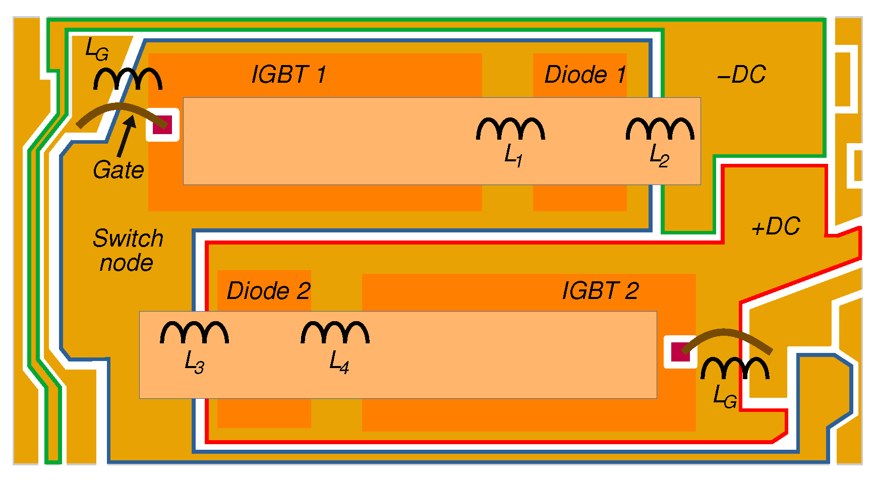
3.1. Parasitic Circuit Element Identification: Analytical Modeling
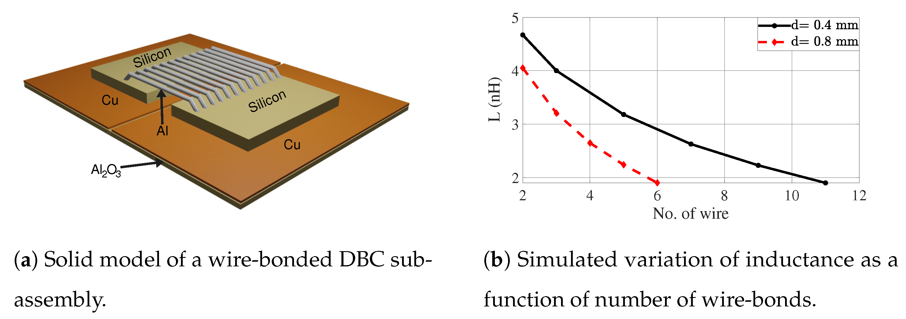
The conventional layout of an IGBT module is shown in Figure 2. Due to the interconnects, the inductances are formed between IGBTs to diodes ( L 1 and L 4 ), diode to—DC ( L 2 ) and diode to Switch node ( L 3 ). Both the Al wire interconnects and the Cu Sinterconnects have been analyzed to estimate the inductances.

3.1.1. Wire Bond

The formation of inductance between two silicon dies (IGBT and diode) due to Al wire bond has been analyzed in two steps. First, the self-inductance ( L s e l f ) of each Al wire has been calculated. Later on, the mutual inductance ( L m ) of each Al bond wire due to the effect of the rest of the bond wires has been calculated. Finally, the equivalent inductance ( L e q ) of the whole interconnects has been calculated.
The self-inductance of a conductor of length l and radius r is given by Equation (1), in which all dimensions are in meters [25].
L s e l f = μ 0 l 2 π l n 2 l r 3 4
The parameters making up Equation (1) were taken to be μ 0 = 4 π × 10 7 A / m , l = 1 mm , r = 150 μ m resulting in L s e l f = 8.3 nH. Furthermore, current flowing through a bond wire, in general, is influenced by the neighboring wires. Therefore, several corresponding mutual inductance values, L m , have been calculated. If the distance between two parallel bond wires is d, the mutual inductance of each bond wire can be calculated by Equation (2) [26].
L m = μ 0 l 2 π l n 2 l d 1
As mentioned earlier, the baseline, wire-bonded sample that has been investigated in this research has n = 12 bond wires. Hence, 11 corresponding L m elements were modeled for each individual wire bond. Given that the spacing between two adjacent bond wires is 0.4 mm and following Equations (1) and (2), the self and mutual inductances of the first bond wire have been calculated and presented in Table 1.
In accounting for all the calculated inductance values L i , i is the self-inductance of each of the n = 12 wire bonds. The mutual inductances between, for example, the first and the rest of the bond wires are captured by the L 1 , 2 , L 1 , 3 L 1 , 12 parameters.
Finally, the total inductance of each of the bond wires can be calculated by Equation (3).
L i = j = 1 n L i j
In Equation (3), n is the number of wire bonds considered, which was 12 in this analysis. Table 2 summarizes the 12 computed L i parameters. Assuming that the bond wires function in parallel, the aggregate, total inductance of the entire interconnect system has been determined to be 3.73 nH using Equation (4).
L = 1 i = 1 12 L i 1

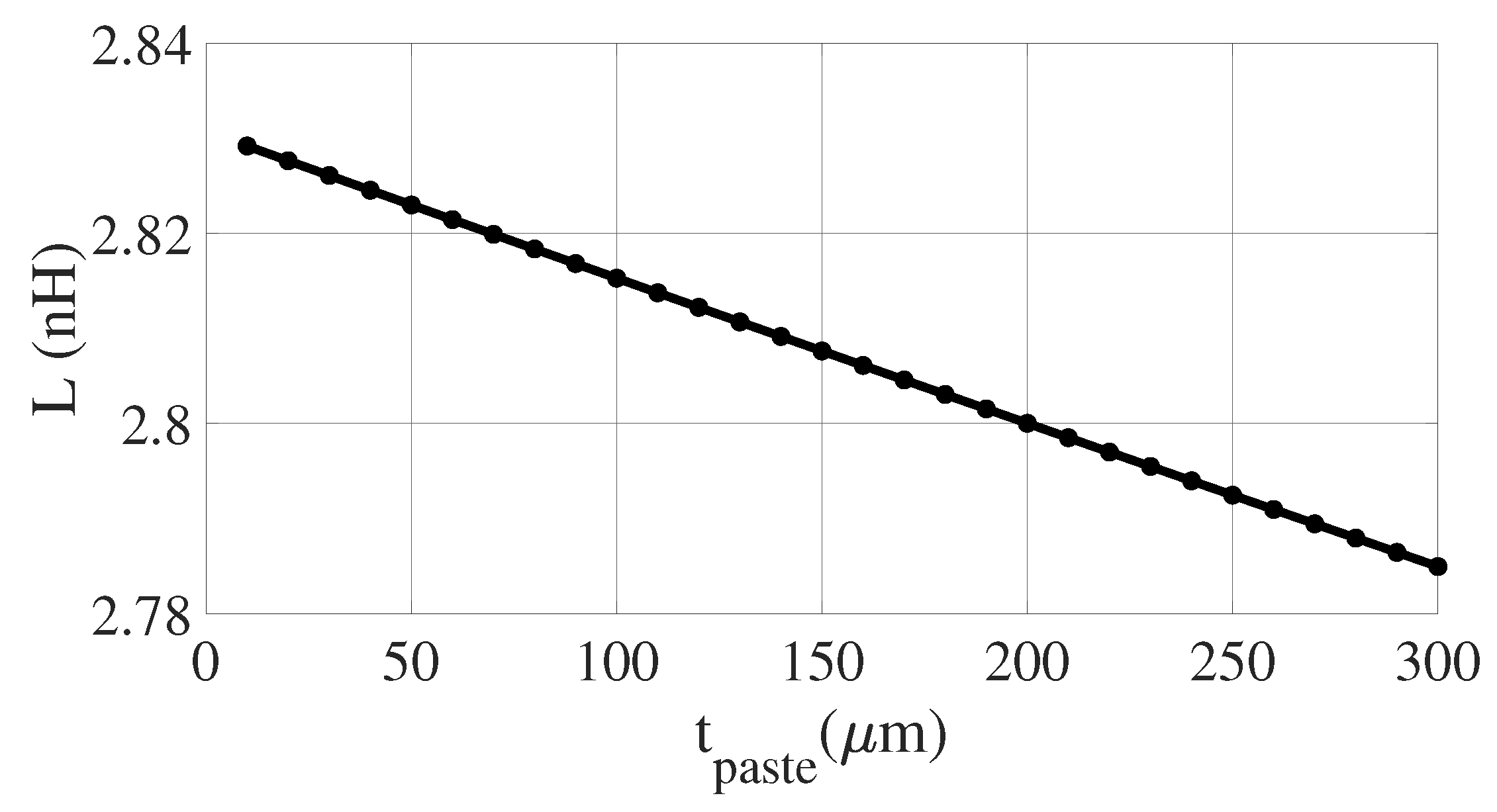
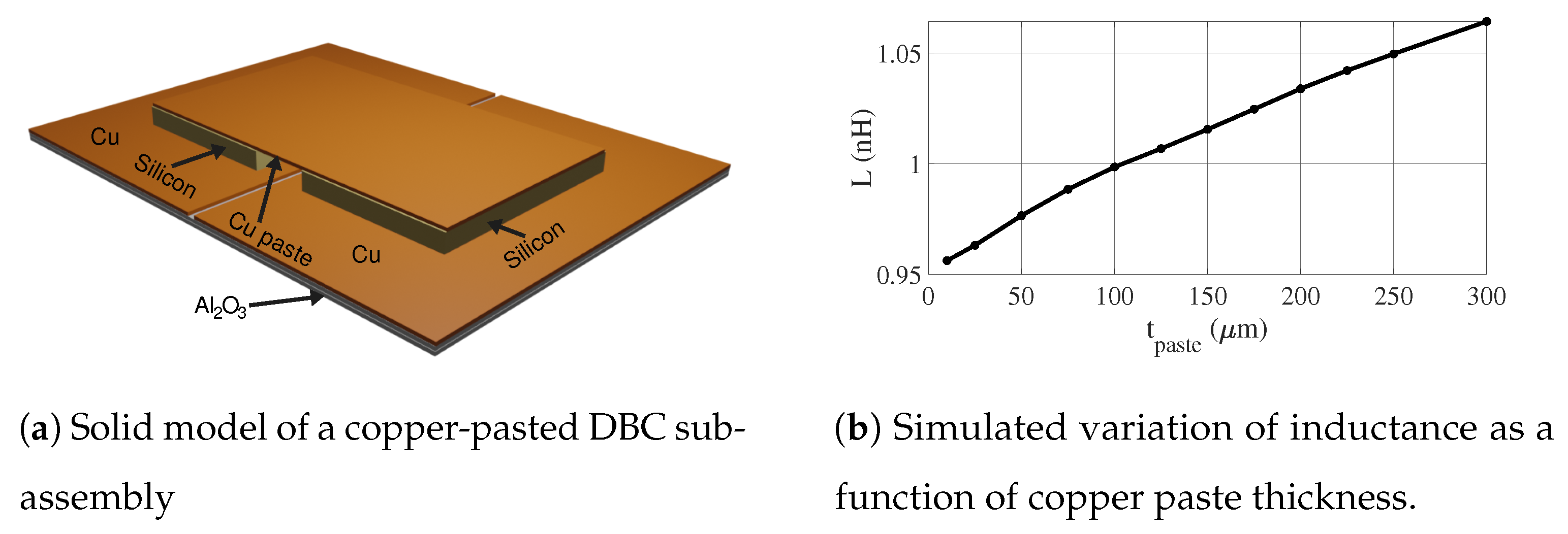
3.1.2. Sinterconnect “Printed Cu”

A formula to estimate the inductance of a thin conductor bar is presented in Equation (5) [25].
L C l i p = μ 0 l 2 π l o g 2 l w + t + 1 2 + 2 9 w + t l
In Equation (5), l , w , and t are the length, width, and thickness of a conductor respectively. In this research, w = 10 mm , l = 10 mm , and t = 100 μ m thick Cu has been considered. By evaluating Equation (5), the inductance of the Cu paste is found to be 2.82 nH. It should be mentioned that in the calculation the total length of the Cu paste has been considered. However, edge-to-edge length is the key driver of inductance. Hence, the inductance in the case of the Cu paste will be less than what we have derived. To evaluate the influence of the thickness of the Cu paste on the inductance formation, variation in thickness of the Cu paste has been evaluated and the results are presented in Figure 3. The parasitic inductance can be seen to vary less than 2%, thus the introduced parasitic inductance is relatively insensitive to Cu paste thickness.

3.1.3. Sinterconnect “Clip-Attach”

In this case, an extra layer of Cu is placed, named as Cu clip, on top of the Cu paste which only increases the thickness of the interconnect. As shown in Figure 3 the thickness of the Cu paste does not have a significant impact on inductance formation, the inductance of this type of connector will be similar to Cu-sinter paste interconnection.

3.2. Parasitic Circuit Element Identification: FE Analysis

In comparison to analytical modeling, FE analysis is able to process physical specimen details and provide high-resolution response data. It is especially suitable for considering power electronic package details in thermal domain analysis [27], as was done for the Sinterconnects in [24]. Now, in order to expand upon the results from Section 3.1, electromagnetic FE simulation has been performed. The objective of the simulation is to estimate the parasitic inductance that formed between the IGBT and the diode. A comparative investigation has been done in the commercial software tool Ansys Maxwell. Simulation convergence is granted by a mesh-refinement based iteration to reduce a global energy error and an energy variation between subsequent iterations steps. In all simulations target values of 1% global error and 1% energy change were undercut in two subsequent iteration steps as break-off criterion.
In the simulations, standard electrical resistivities ρ C u = 1.68 × 10 8 Ω m and ρ A l = 2.63 × 10 8 Ω m have been used for Cu and Al, respectively. For Si components, the resistivity of highly doped Si ( ρ S i - d o p e d = 1 × 10 5 Ω m ) was considered. For the aluminium oxide (Al 2 O 3 ) part, standard Ansys maxwell parameters have been utilized.

3.2.1. Wire Bond

First, the simulation has been performed on Al wire bond interconnects. The simulation model and the results are shown in Figure 4. The variation of L is analyzed with respect to the number of parallel wires and the distance between two adjacent wire (d). Figure 4b shows that, as the number of parallel Al interconnect wires increases, the inductance decreases. However, as the distance between two adjacent interconnect decreases, the equivalent inductance increases. In addition, it can be seen that with a standard wire separation distance of 800 μ m , 6 parallel Al bond wires exhibit an equivalent inductance of 1.8 nH. On the contrary, to reach the same inductance value, 11 Al wire will be needed with a separation distance of 400 μ m .

3.2.2. Sinterconnect “Printed Cu”

In this case, the simulations have been done by replacing the Al wire with Cu paste. During the simulations, Cu paste thickness has been varied from 10 μ m to 300 μ m to understand the effect of Cu paste thickness on the inductance formation. The simulation model and the results are presented in Figure 5. In Figure 5b, it can be seen that the variation of Cu thickness does not have a significant impact on inductance creation; throughout the ranges of Cu thickness, the inductance is around 1 nH.

3.2.3. Sinterconnect “Clip-Attach”

As explained earlier, in this configuration, an additional 100 μ m thick layer of Cu is placed on top of the Cu paste interconnect. Hence, the simulation results of Section 3.2.2 could also be representative of the Cu clip interconnect structure. Given that, the additional Cu clip only increases the thickness of the interconnect which does not have a significant impact on inductance values.
From the above investigation, it can be summarized that, in the case of using both Sinterconnects (printed Cu and clip-attach), the parasitic inductances can be significantly reduced. The reduction of inductance from 1.8 nH (Al wire bond) to 1.0 nH (Sinterconnects) will have a significant impact on power converters in high-frequency switching applications.

3.3. Resistivity

To compare the performance of the three different systems, electrostatic (DC conduction) simulations have been carried out via Ansys Maxwell. To this aim, the electrical resistance (R) of the two Sinterconnect systems have been computed for the ideal ( ρ c u P a s t e = 3 × ρ C u ) and the worst ( ρ c u P a s t e = 10 × ρ C u ) measured electrical conductivity of the Cu paste material and compared with the resistance of wire bond system. Results show that the “clip-attach” system exhibits a R c l i p = 0.27 m Ω for ρ c u P a s t e = 3 × ρ C u ( R c l i p = 0.31 m Ω for ρ c u P a s t e = 10 × ρ C u ) outperforming compared to the “printed Cu” and the wire bond systems having resistances of R p r i n t e d C u = 0.55 m Ω for ρ c u P a s t e = 3 × ρ C u ( R p r i n t e d C u = 1.18 m Ω for ρ c u P a s t e = 10 × ρ C u ) and R w i r e = 0.94 m Ω , respectively. In addition, the electrical resistance has been investigated for the “clip-attach” Sinterconnect system as a function of the thickness of the Cu-clip. As expected, since the resistance is proportional to the length of the of Cu clip and it is inversely proportional to its cross section, this analysis shows that the resistance of the “clip-attach” system can be further decreased by increasing the thickness of the Cu-clip [24].

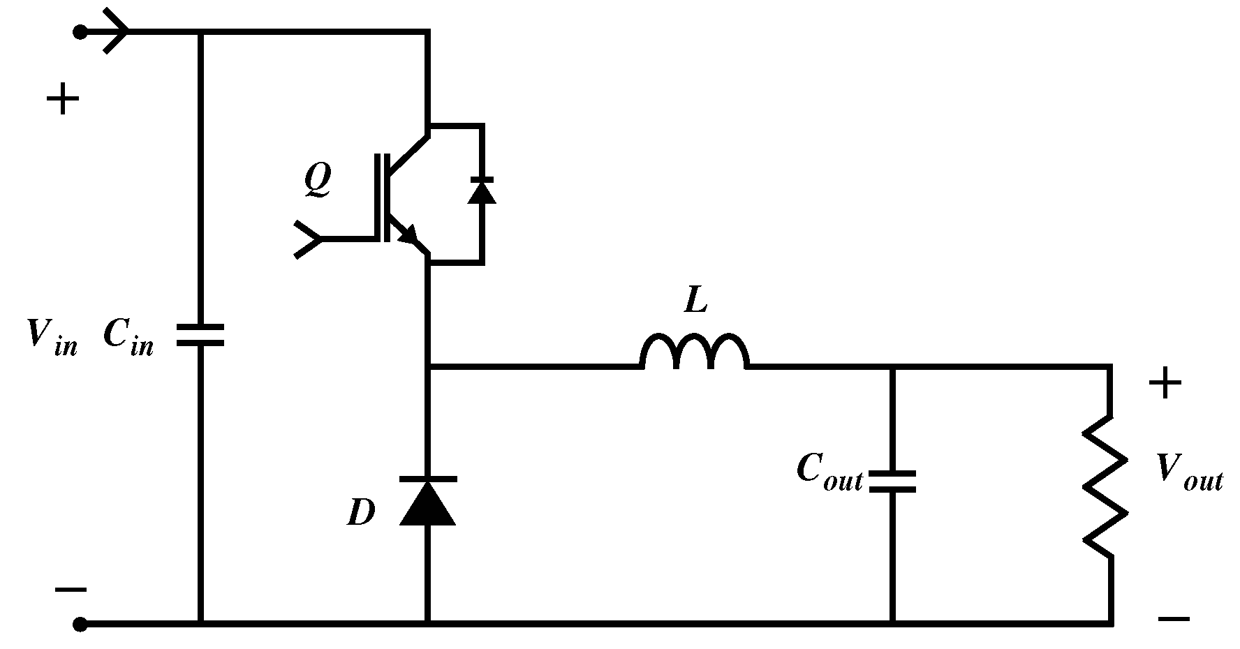
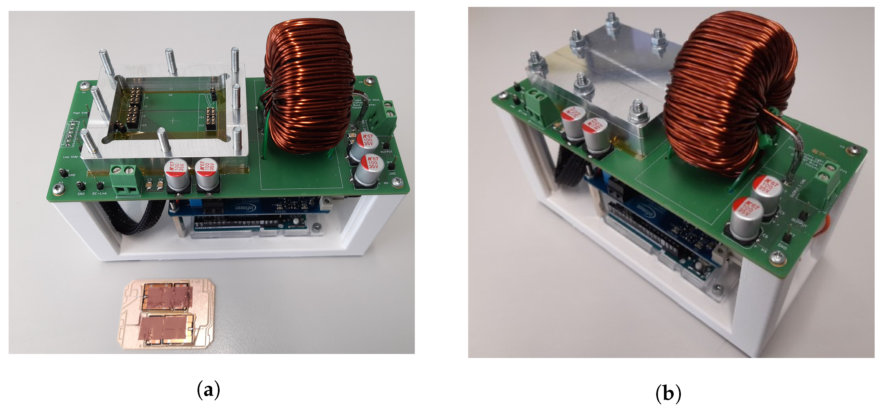
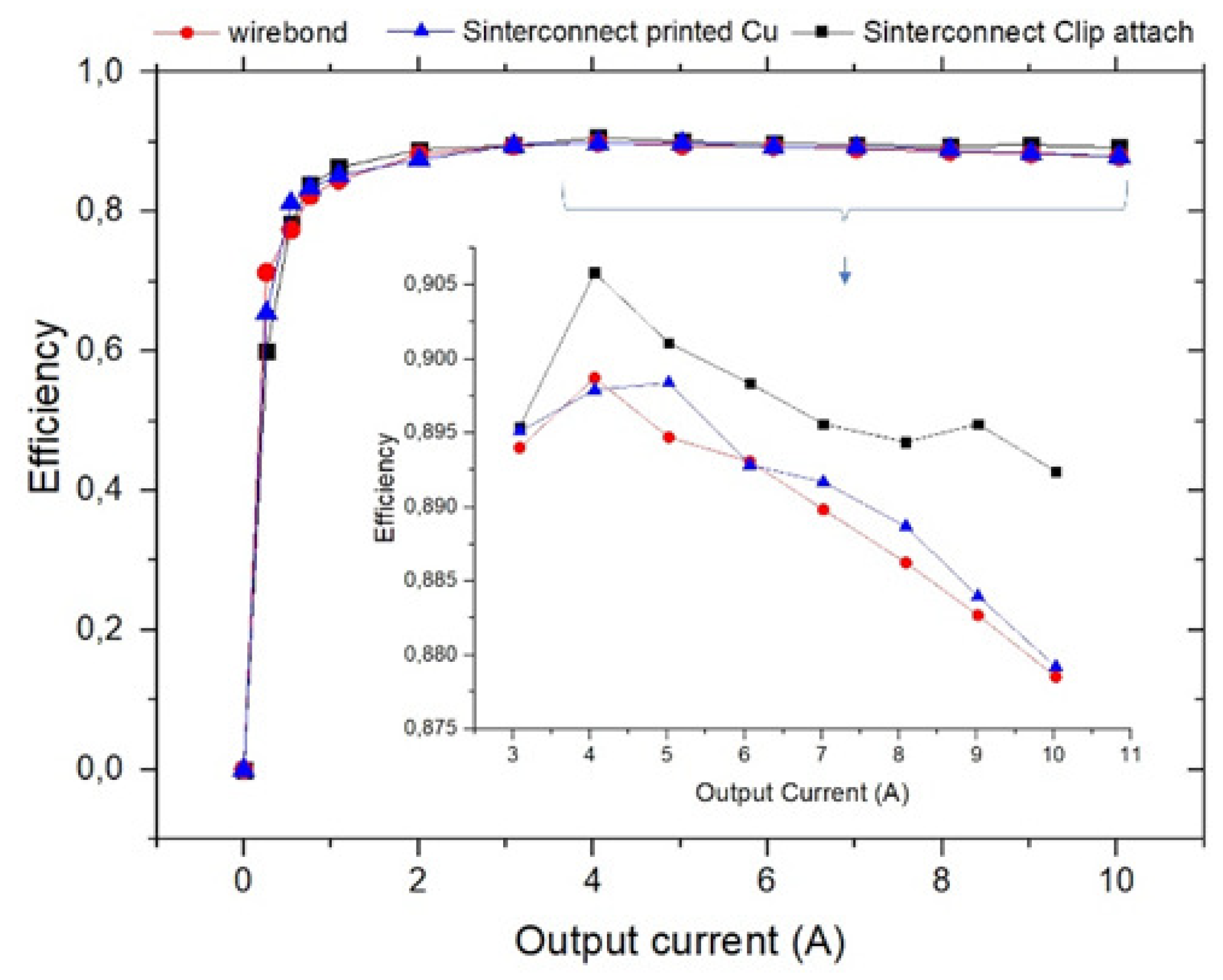
3.4. System Level Performance

To quantify the impact of the Sinterconnected IGBT module on system-level, power conversion performance, a power electronic test circuit has been designed and prototyped. Selected for prototyping is a conventional buck converter, as shown schematically in Figure 6, which is a fundamental building block to other more complex power electronic circuit topologies, such as those in [28]. The buck converter parameters are presented in Table 3.
To evaluate the individual performance of different types of interconnects, each device has been utilized as a switching device. The power conversion efficiency of the converter has been analyzed then. Since only the switching device is being changed for each evaluation, the comparison should be considered fair. The experimentally realized converter with a sample IGBT module is shown in Figure 7. Figure 7a shows the sample and the converter setup which includes a customized holder to place the IGBT module in the converter. The electrical contacts between IGBT and converter are established using spring-loaded connectors. Figure 7b shows the converter where the IGBT sample is placed and covered in the converter.
The performance evaluation has been done for wire bond samples and both types of Sinterconnect samples. Several samples (>3 per kind) were fabricated and evaluated.
A switching frequency of 4.6 kHz has been used during these tests (the working frequency of the IGBT modules). The experimental results shows that throughout the current range of 2 A to 10 A, all samples provide an efficiency of approximately 88–90%. The output current ( I o u t ) versus efficiency ( η ) is plotted in Figure 8. As inferred from this figure, clip-attach samples possess a slightly better performance than the others, whereas the printed Cu shows comparable efficiencies to wire-bonded IGBT modules. According to our simulation results, the Sinterconnect advantage towards wire bond is more pronounced in higher switching frequencies (such as in MOSFET or GaN modules); however, for the utilized IGBT modules the frequency range is rather limited to 4.6 kHz. Nonetheless, even for this module, the Sinterconnects shows comparable and even higher performances in terms of efficiency. Principally, Cu-attach Sinterconnects renders slightly higher efficiencies than printed Cu Sinterconnects. On the other hand, from the fabrication point of view, printed Cu Sinterconnects are much easier to process and more cost-effective.

4. Conclusions

In this study, printed Cu front-side interconnect “Sinterconnects” were benchmarked versus Al thick wire bonds as DC-DC converters. Building upon [24], this paper has carefully analyzed Sinterconnect geometries to estimate parasitic inductance parameters and measured the efficiency of a switch-mode, DC-DC converter employing Sinterconnected IGBT power modules. These Sinterconnects can easily be fabricated at any back-end (power packaging) facility by using a dispensing or jetting unit. Theoretical analysis suggests, that by using the Sinterconnects, the total package stray inductance can be reduced by around 25%. Finite element analysis revealed the high package inductance sensitivity to the total number of wire bonds as well as the distance between two adjacent bond wires and the desired insensitivity of the Sinterconnects to Cu layer thickness. According to the experimental results, the buck converters having Sinterconnected IGBT modules showed better or at least comparable performance to a wire-bond interconnected module. The higher performance of the clip-attach sample could be attributed to the lower electrical resistance of the Cu clip compared to Cu paste through the application of the Cu foil. In this work, the switching characteristics of the device and the efficiency of the converter have been analyzed at 4.6 kHz. In a follow-up study, the performance of Sinterconnects at higher switching frequencies and their reliability analysis will be investigated.

Author Contributions

Conceptualization, A.R. and A.B.; methodology, M.N.H., T.P. and D.H.; software, P.M.; validation A.R. and T.P.; investigation, A.R., D.H., T.P. and M.N.H.; writing—original draft preparation M.N.H., T.P. and A.R.; writing—review and editing, A.R., T.P., D.H. and P.M.; supervision, A.B.; project administration, A.R.; funding acquisition, A.B. All authors have read and agreed to the published version of the manuscript.

Funding

This study has been performed in the frame of the Power2power program. Power2Power is a European co-funded innovation project on Semiconductor Industry. The project receives grants from the European H2020 research and innovation program, ECSEL Joint Undertaking, and National Funding Authorities from eight involved countries under grant agreement No. 826417. The participating countries are Austria, Finland, Germany including the Free States of Saxony and Thuringia, Hungary, the Netherlands, Slovakia, Spain and Switzerland.

Institutional Review Board Statement

Not applicable.

Informed Consent Statement

Not applicable.

Data Availability Statement

Not applicable.

Conflicts of Interest

The authors declare no conflict of interest. The funders had no role in the design of the study; in the collection, analyses, or interpretation of data; in the writing of the manuscript, or in the decision to publish the results.

References

  1. Ramminger, S.; Seliger, N.; Wachutka, G. Reliability model for Al wire bonds subjected to heel crack failures. Microelectron. Reliab. 2000, 40, 1521–1525. [Google Scholar] [CrossRef]
  2. Liu, K.; Yang, J.; Luo, J.; Wang, L.; Huang, Q.; Chen, F. The characterization and application of chip topside bonding materials for power modules packaging: A review. J. Phys. Conf. Ser. 2020, 1605, 012168. [Google Scholar] [CrossRef]
  3. Durand, C.; Klingler, M.; Coutellier, D.; Naceur, H. Power cycling reliability of power module: A survey. IEEE Trans. Device Mater. Reliab. 2016, 16, 80–97. [Google Scholar] [CrossRef]
  4. Wirebondless Semiconductor Package. U.S. Patent US8304903B2, 6 November 2012.
  5. Wirebondless Module Package. U.S. Patent US5616886A, 5 June 1995.
  6. Wirebondless Wafer Level Package with Plated Bumps and Interconnects. U.S. Patent US20090289356A1, 23 May 2008.
  7. Weidner, K.; Kaspar, M.; Seliger, N. Planar interconnect technology for power module system integration. In Proceedings of the 7th International Conference on Integrated Power Electronics Systems (CIPS), Nuremberg, Germany, 6–8 March 2012; pp. 1–5. [Google Scholar]
  8. Hain, S.; Bakran, M.-M.; Jaeger, C.; Niedernostheide, F.-J.; Domes, D.; Heer, D. The effect of different stray inductances on the performance of various types of IGBTs—Is less always better? In Proceedings of the 17th European Conference on Power Electronics and Applications (EPE’15 ECCE-Europe), Geneva, Switzerland, 8–10 September 2015; pp. 1–9. [Google Scholar]
  9. Hoene, E.; Ostmann, A.; Marczok, C. Packaging very fast switching semiconductors. In Proceedings of the CIPS 2014, 8th International Conference on Integrated Power Electronics Systems, Nuremberg, Germany, 25–27 February 2014; pp. 1–7. [Google Scholar]
  10. Ciappa, M.; Fichtner, W. Lifetime prediction of IGBT modules for traction applications. In Proceedings of the IEEE International Reliability Physics Symposium Proceedings, 38th Annual (Cat. No. 00CH37059), San Jose, CA, USA, 10–13 April 2000; pp. 210–216. [Google Scholar]
  11. Deng, E.; Zhao, Z.; Xin, Q.; Zhang, J.; Huang, Y. Analysis on the difference of the characteristic between high power IGBT modules and press pack IGBTs. Microelectron. Reliab. 2017, 78, 25–37. [Google Scholar] [CrossRef]
  12. Polom, T.A.; Broeck, C.H.V.; Doncker, R.W.D.; Lorenz, R.D. Spatially-varying electrothermal impedance analysis for designing power semiconductor converter systems. In Proceedings of the 18th IEEE Intersociety Conference on Thermal and Thermomechanical Phenomena in Electronic Systems (ITherm), Las Vegas, NV, USA, 28–31 May 2019; pp. 117–126. [Google Scholar]
  13. Siepe, D.; Bayerer, R.; Roth, R. The future of wire bonding is? Wire bonding! In Proceedings of the CIPS 2010—6th International Conference on Integrated Power Electronics Systems, Nuremberg, Germany, 16–18 March 2010. [Google Scholar]
  14. Liu, P.; Tong, L.; Wang, J.; Shi, L.; Tang, H. Challenges and developments of Cu wire bonding technology. Microelectron. Reliab. 2012, 52, 1092–1098. [Google Scholar] [CrossRef]
  15. Chang, H.-R.; Bu, J.; Kong, G.; Labayen, R. 300 A 650 V 70 μm thin IGBTs with double-sided cooling. In Proceedings of the IEEE 23rd International Symposium on Power Semiconductor Devices and ICs, San Diego, CA, USA, 23–26 May 2011; pp. 320–323. [Google Scholar]
  16. Ikeda, Y.; Iizuka, Y.; Hinata, Y.; Horio, M.; Hori, M.; Takahashi, Y. Investigation on wirebond-less power module structure with high- density packaging and high reliability. In Proceedings of the IEEE 23rd International Symposium on Power Semiconductor Devices and ICs, San Diego, CA, USA, 23–26 May 2011; pp. 272–275. [Google Scholar]
  17. Ozmat, B.; Korman, C.; McConnelee, P.; Kheraluwala, M.; Delgado, E.; Fillion, R. A new power module packaging technology for enhanced thermal performance. In Proceedings of the ITHERM 2000, the Seventh Intersociety Conference on Thermal and Thermomechanical Phenomena in Electronic Systems (Cat. No. 00CH37069), Las Vegas, NV, USA, 23–26 May 2000; Volume 2, pp. 287–296. [Google Scholar]
  18. Beckedahl, P.; Hermann, M.; Kind, M.; Knebel, M.; Nascimento, J.; Wintrich, A. Performance comparison of traditional packaging technologies to a novel bond wire less all sintered power module. In Proceedings of the PCIM Europe, Nuremberg, Germany, 17–19 May 2011; pp. 247–252. [Google Scholar]
  19. Event: Packaging Day 2010; Fraunhofer Institute of Reliability and Microeletronics IZM: Berlin, Germany, 8 July 2010.
  20. Zhu, Q.; Forsyth, A.; Todd, R.; Mills, L. Thermal characterisation of a Cu-clip-bonded IGBT module with double-sided cooling. In Proceedings of the 23rd International Workshop on Thermal Investigations of ICs and Systems (THERMINIC), Amsterdam, The Netherlands, 27–29 September 2017; pp. 1–6. [Google Scholar]
  21. Barbarini, E.; Troadec, C. Power module packaging: Market and technology trends. In Proceedings of the Additional Conferences (Device Packaging, HiTEC, HiTEN, & CICMT), Samos, Greece, 7–11 July 2019; Volume 2019, pp. 000749–000779. [Google Scholar] [CrossRef]
  22. Lee, H.; Smet, V.; Tummala, R. A review of sic power module packaging technologies: Challenges, advances, and emerging issues. IEEE J. Emerg. Sel. Top. Power Electron. 2019, 8, 239–255. [Google Scholar] [CrossRef]
  23. Stockmeier, T.; Beckedahl, P.; Göbl, C.; Malzer, T. Skin: Double side sintering technology for new packages. In Proceedings of the IEEE 23rd International Symposium on Power Semiconductor Devices and ICs, San Diego, CA, USA, 23–26 May 2011; pp. 324–327. [Google Scholar]
  24. Roshanghias, A.; Malago, P.; Kaczynski, J.; Polom, T.; Bardong, J.; Holzmann, D.; Malik, M.-H.; Ortner, M.; Hirschl, C.; Binder, A. Sinterconnects: All-Cu top-side interconnects based on Cu sinter paste for power module packaging. Energies 2021, 14, 2176. [Google Scholar] [CrossRef]
  25. Grover, F.W. Inductance Calculations: Working Formulas and Tables; Dover Publication Inc.: Mineola, NY, USA, 1946. [Google Scholar]
  26. Caniggia, S.; Maradei, F. Signal Integrity and Radiated Emission of High-Speed Digital Systems; John Wiley & Sons: Hoboken, NJ, USA, 2008. [Google Scholar]
  27. Polom, T.A.; Broeck, C.H.V.; Doncker, R.W.D.; Lorenz, R.D. Designing power module health monitoring systems based on converter load profile. IEEE Trans. Ind. Appl. 2020, 56, 6711–6721. [Google Scholar] [CrossRef]
  28. Hasan, M.N.; Polom, T.A. Comparative study between the Ćuk and the LLC converter in photovoltaic applications. In Proceedings of the IEEE 15th International Conference on Compatibility, Power Electronics and Power Engineering (CPE-POWERENG), Florence, Italy, 14–16 July 2021; pp. 1–8. [Google Scholar]
Figure 1. Top-side interconnect structure depictions on DBC subassemblies; (a) wire bond, (b) Sinterconnect “printed Cu” and (c) Sinterconnect “clip attach”.
Electronics 11 01373 g001
Figure 2. Top view of a DBC sub-assembly with Sinterconnects indicating the main parasitic inductances.
Electronics 11 01373 g002
Figure 3. Influence of Cu thickness on its equivalent parasitic inductance.
Electronics 11 01373 g003
Figure 4. FE analysis of the wire bonds (a) the model and (b) the dependence of inductance on the number of wires and distance between two wires.
Electronics 11 01373 g004
Figure 5. FE analysis of the Sinterconnects (a) the model and (b) the dependence of inductance on the Cu thickness.
Electronics 11 01373 g005
Figure 6. Buck converter schematic.
Electronics 11 01373 g006
Figure 7. IGBT buck converter hardware photographs with control board (blue) underneath the main power board (green) having bulk energy storage capacitor and inductor components. (a) View with the IGBT-DBC half-bridge removed and not installed on the power board. (b) View with the DBC half-bridge mounted against the spring pressure contacts.
Electronics 11 01373 g007
Figure 8. Measured buck converter efficiency values.
Electronics 11 01373 g008
Table 1. Self and mutual inductance of the first bond wire.
Self and Mutual Inductances (nH)
L 1 , 1 L 1 , 2 L 1 , 3 L 1 , 4 L 1 , 5 L 1 , 6 L 1 , 7 L 1 , 8 L 1 , 9 L 1 , 10 L 1 , 11 L 1 , 12
8.28575.82404.43783.62683.05152.60522.24051.93221.66521.42961.21891.0283
Table 2. Equivalent inductance of each bond wire.
Equivalent Inductance of Each Bond Wire (nH)
L 1 L 2 L 3 L 4 L 5 L 6 L 7 L 8 L 9 L 10 L 11 L 12
37.34642.14145.36047.55748.94449.61749.61748.94447.55745.36042.14137.346
Table 3. Buck converter specifications.
ParametersRangeNominal Values
Input voltage12   V –24   V 18   V
Output voltage6   V –12   V 9   V
Duty cycle 0.5
Switching frequency 4.6   kHz
Output power1   W –120   W 80   W
Publisher’s Note: MDPI stays neutral with regard to jurisdictional claims in published maps and institutional affiliations.

