Article

Synthesis of Wideband All-Frequency Absorptive Filtering Power Divider with High Selectivity and Flat Output Port Distributions

School of Information Science and Technology, Dalian Maritime University, Dalian 116026, China
*
Author to whom correspondence should be addressed.
Electronics 2023, 12(17), 3704; https://doi.org/10.3390/electronics12173704
Submission received: 1 August 2023 / Revised: 23 August 2023 / Accepted: 30 August 2023 / Published: 1 September 2023
(This article belongs to the Section Microwave and Wireless Communications)

Abstract

:
In this paper, a wideband absorptive filtering power divider (AFPD) which features the characteristics of high selectivity and flat output distributions is proposed. It is composed of one unequal width three-coupled line (TCL), two coupled lines (CLs), two stepped open-circuited stubs, two kinds of isolation resistors, and two types of absorptive branches. The design equations of the proposed AFPD are derived using an even-odd decomposition method, and parametric investigations are also performed. It is found that the passband bandwidth can be adjusted by the stepped open-circuited stub which generates two transmission zeros (TZs). By combining the TCL with the CLs, the passband bandwidth is effectively enlarged. In addition, two isolated resistors are utilized for achieving good isolation and output-port matching performance. Without affecting the passband responses, the input port absorptive feature within the whole frequency band can be obtained by loading the absorptive branches both on the input and output ports. For validation, an example operating at the center frequency of 2 GHz was modeled and tested. Results exhibit that the passband FBW reaches 72% under 1 dB criterion, which illustrates flat output port distributions. In addition, for 10 dB return loss, the input and output impedance matching bandwidths are 250% and 78%, respectively. The features of good filtering responses are demonstrated by realizing the rectangle coefficient of 1.24 and the out-of-band suppression of more than 20 dB.

1. Introduction

Filtering power dividers (FPDs), which integrate the functions of frequency selectivity and power division, have been a hot topic in recent years. Compared with the cascading configuration of power dividers and filters, the FPDs [1,2,3,4,5,6,7,8,9,10] have the merits of smaller size, better performance, and lower insertion loss. The research on FPDs has involved the wideband [1,2,3,4,5,6,7,8], dual-band [3,4,5], multi-way [6,7,8,9], reconfigurable [10], and so on. However, the FPDs introduced above are all reflective-type bandpass filters (BPFs), which means that the un-transmitted RF-input signal in the stopband regions will be reflected back to the source and affect the performance of adjacent active stages, such as the power amplifiers [11], the multiplexer [12], and so on. Inspired from the absorptive filters [13,14,15,16,17], the FPDs with input-absorptive behavior can be a good solution to deal with the above problem.
Until now, only several studies have reported on absorptive FPDs (AFPDs). In [18], the absorptive natures at the input/output ports are achieved by loading resistively terminated bandstop filtering branches. The passband 3 dB fractional bandwidth (FBW) is 13.6% and the 10 dB absorptive FBW is 75.5%. In [19], a frequency reconfigurable input-absorptive FPD is designed by replacing the λ/4 segments in PD arms with tunable BPFs and connecting the tunable bandstop filtering branch to the input port as the complementation. During the 28.1% frequency tuning range, the 3 dB FBW at each tuning state is 11.6%, and the 10 dB absorptive FBW reaches 87%. However, the above reports both have the drawbacks of narrow bandwidth, poor selectivity, and large dimensions.
To widen the operating bandwidth and improve the selectivity, two cascaded coupled lines (CLs) loaded with λ/2 open-circuited stubs are applied in designing the FPD in [20]. In addition, all-frequency input-absorption is realized by using three λ/4 short-circuited stubs series with resistors. Measurement results indicate that the in-band FBW is 62.3% for 10 dB return loss, and the stopband suppression reaches more than 20 dB. In addition, the absorptive bandwidth under 10 dB return loss reaches 200%. However, the passband 3 dB FBW is only 46%. When using 1 dB FBW as the criterion, the FBW is reduced to 25.9%, which indicates poor flatness. In [21], a compact wideband absorptive FPD is proposed. It exhibits the wideband filtering and power division functions by using the three-coupled lines (TCLs). In addition, the wideband input-absorptive feature is achieved by combining the T-shaped network with the absorptive stub. The 1 dB FBW is 52.8%, and the 10 dB input-absorptive band reaches 200%. The only drawback is the poor output matching bandwidth, which is narrower than the 1 dB FBW.
In the paper, an AFPD is presented with the advantages of wide passband bandwidth, wide input absorptive bandwidth, wide output impedance matching bandwidth, high selectivity, and flat output distributions. The main innovation of the proposed AFPD is the loading of two absorptive branches and the combination with suitable filtering sections, including the TCL, the CLs, and the stepped open-circuited stubs, to achieve a wideband absorptive bandwidth and at the same time keep good filtering responses, good output port impedance matching, and flat output distributions. A prototype was fabricated for validation. During the measurement, the FBWs for 1 dB and 3 dB passband criterions are 72% and 85%, respectively, with more than a 20 dB out-of-band suppression level. Using 10 dB return loss as the criterion, the input and output port impedance matching bandwidths are 250% and 78%, respectively. In addition, the rectangle coefficient (RC) reaches 1.24, which indicates high selectivity. In Section 2, the proposed AFPD is analyzed and parametric investigations are carried out. The implementation and measurements of the designed AFPD are shown in Section 3. Finally, Section 4 concludes the paper.

2. Theoretical Analysis and Design Procedure

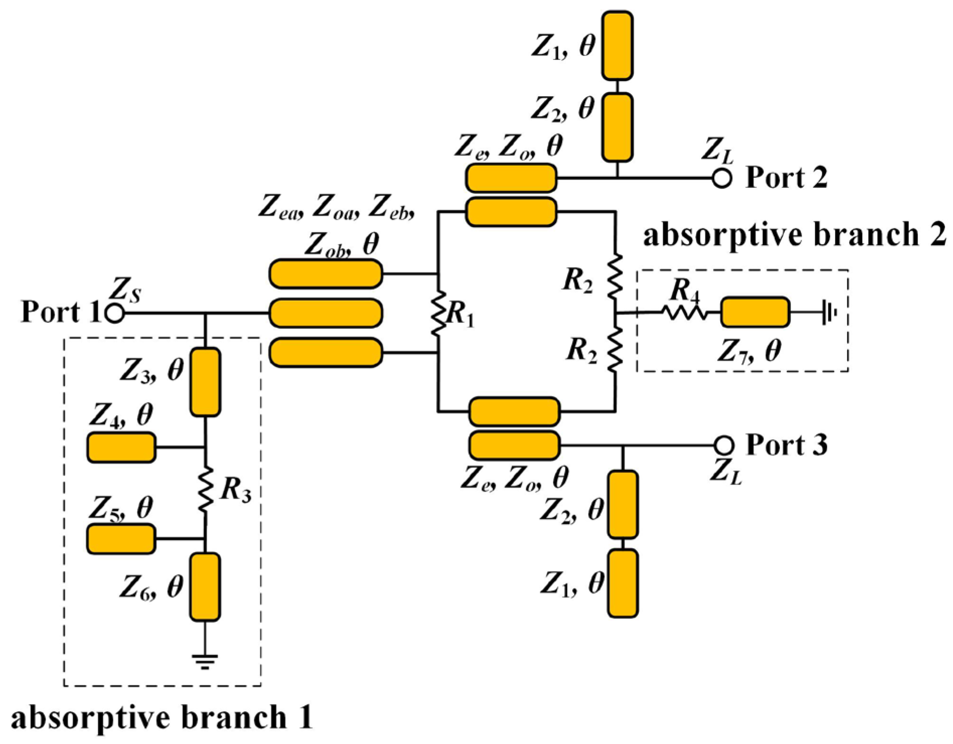
2.1. Schematic of the AFPD

The topology of the proposed AFPD is illustrated in Figure 1. It consists of one unequal width TCL, two CLs, two stepped open-circuited stubs, two kinds of isolation resistors (R1 and R2), and two types of absorptive branches. One of the absorptive branches is loaded on the input port of the AFPD and consists of two L-shaped microstrip structures connected by a loss resistor (R3). The other absorptive branch, which is composed of a λ/4 short-circuited stub and a lossy resistor (R4), is shunted on the middle of the two isolation resistors, R2. By using the TCL combined with the two CLs, a wide passband 3 dB FBW can be achieved. In addition, two transmission zeros (TZs) appear by shunting the stepped open-circuited stubs, and the frequency selectivity is simultaneously improved. The loading of absorptive branches enables the behavior of input-absorption and increases the out-of-band suppression. Good isolation and output port matching can also be achieved by inserting resistors R1 and R2.
In the following, the circuit parameters of the proposed AFPD are introduced in detail. Firstly, the electrical lengths of the lines in Figure 1 are all defined as θ and correspond to 90° at the center frequency. Let Ze be the even-mode impedance of the CL, and let Zo be the odd-mode impedances of the CL. Since the TCL is composed of CLs with unequal widths, asymmetric CLs are utilized for the analysis of the TCL. Here, four parameters (Zea, Zoa, Zeb and Zob) are applied for the expression of the couplings between the edge and center lines. In detail, Zea and Zoa are the impedances of the edge line under even- and odd-mode excitations, respectively, while Zeb and Zob denote the impedances of the center line under even- and odd-mode cases, separately. The stepped open-circuited stub consists of two kinds of transmission lines (TLs) with the characteristic impedances of Z1 and Z2. The isolation resistor named as R1 is shunted between the nonadjacent lines of the TCL. Two isolation resistors, R2, are in series between the terminals of the two CLs. In the absorptive branch, the first L-shaped structure includes a TL (Z3) and an open-circuited stub (Z4), while the other L-shaped structure is composed of an open-circuited stub (Z5) and a short-circuited stub (Z6). For the other absorptive branch, the characteristic impedance of the short-circuited stub is defined as Z7.

2.2. Analysis of the FPD

2.2.1. Design Equations

Firstly, the AFPD without the absorptive branches (named as FPD) is analyzed. Figure 2 shows its sub-circuits under even-odd mode analysis. From the variables exhibited in Figure 2, the port impedances of the FPD under the odd- and even-mode cases (ZTRino, ZTLine, and ZTRine) can be derived as (1).
Z TRino = Z TRo 3 Z Y Z TRo 3 + Z Y
Z TLine = Z S 2 2 Z S 6 2 Z S 1 + Z S 7 + Z TLe 1
Z TRine = Z Y ( Z 33 Z 11 + Z 33 Z TRe 1 Z 13 Z 31 ) Z Y ( Z 11 + Z TRe 1 ) + ( Z 33 Z 11 + Z 33 Z TRe 1 Z 13 Z 31 )
Here, the ZTRino is the impedance viewed from port 2 under odd-mode case, and ZTrine is the impedance viewed from port 2 under even-mode case. ZTLine represents the impedance viewed from port 1 under even-mode case. In addition, ZY is the input impedance of the stepped open-circuited stub, ZTRo3 is the input impedance looking in from the right end of the CL in the odd-mode excitation. ZTLe1 and ZTRe1 are the input impedances looking in from the left end of the CL and the right end of the TCL, respectively, in the even-mode case. The expressions of ZY, ZTRo3, ZTLe1, and ZTRe1 are shown in (2).
Z Y = j Z 2 Z 2 tan θ Z 1 cot θ Z 1 + Z 2
Z TRo 3 = Z 33 Z 34 Z 43 Z 44 + R 2 ( Z 13 Z 44 + Z 13 R 2 Z 34 Z 14 ) 2 ( Z TRo 2 + Z 11 ) ( Z 44 + R 2 ) 2 Z 14 Z 41 ( Z 44 + R 2 )
Z T L e 1 = Z 11 Z 13 Z 31 ( Z Y + Z 0 ) Z Y Z 0 + Z 33 ( Z Y + Z 0 )
Z T R e 1 = Z S 1 + Z S 7 + 2 Z S 6 2 Z S 2 + Z 0
The intermediate variable ZTRo3 in (2b) can be expressed in (3), which denotes the input impedance looking in from the connection node of the right end of the TCL and the resistor R1.
Z TRo 2 = ( Z S 1 Z S 2 + Z S 2 Z S 7 Z S 6 2 ) R 1 2 ( Z S 1 Z S 2 + Z S 2 Z S 7 Z S 6 2 ) + Z S 2 R 1
Except for the mentioned variables, the variables Z11, Z13, Z14, Z31, Z33, Z34, Z41, and Z44 are the self-impedances of the CL [22], while the variables ZS1, ZS2, ZS6, and ZS7 are the self-impedances of the TCL [23]. The expressions of the self-impedances are shown in (4). Here, the Ze and Zo in (4a) are defined as the even- and odd-mode characteristic impedances of the CL. In (4b) and (4c), the Zea and Zoa are the impedances of the edge line under even- and odd-mode cases, respectively. Zeb and Zob denote the impedances of the center line for even- and odd-mode cases, separately.
{ Z 11 = Z 33 = Z 44 = j Z e + Z o 2 cot θ Z 13 = Z 31 = j Z e Z o 2 csc θ Z 14 = Z 41 = j Z e + Z o 2 csc θ Z 34 = Z 43 = j Z e Z o 2 cot θ
{ Z S 1 = j Z e a + Z o a 2 cot θ Z S 2 = j Z e b + Z o b 2 cot θ Z S 6 = j Z e a Z o a 2 csc θ Z S 7 = j K ( Z e a Z o a ) 2 cot θ
Z e a Z o a = Z e b Z o b
Here, note that in order to obtain a wideband response, the value of K is often chosen within 0.3–0.7, and it is set to 0.5 as the average value in the design as [24]. Then, the input impedance matching and transmission performance (S11_FPD and S21_FPD) of the FPD can be obtained as (5) [20].
S 11 _ FPD = Γ i n e = Z T L i n e Z 0 Z T L i n e + Z 0
S 21 _ FPD = S 31 _ FPD = 1 2 S 21 e
S 22 _ FPD = Γ o u t e + Γ o u t o 2 = Z T R i n e Z T R i n o Z 0 2 ( Z T R i n e + Z 0 ) ( Z T R i n o + Z 0 )
S 23 _ FPD = Γ o u t e Γ o u t o 2 = Z 0 Z T R i n e Z 0 Z T R i n o ( Z T R i n e + Z 0 ) ( Z T R i n o + Z 0 )
Here, Z0 is reference impedance which is equal to 50 Ω in general. Γine represents the reflection performance of the input port for even-mode case. Γoute and Γouto are the reflection coefficients of the output ports (port 2 or 3) under even- and odd-mode excitation, respectively.

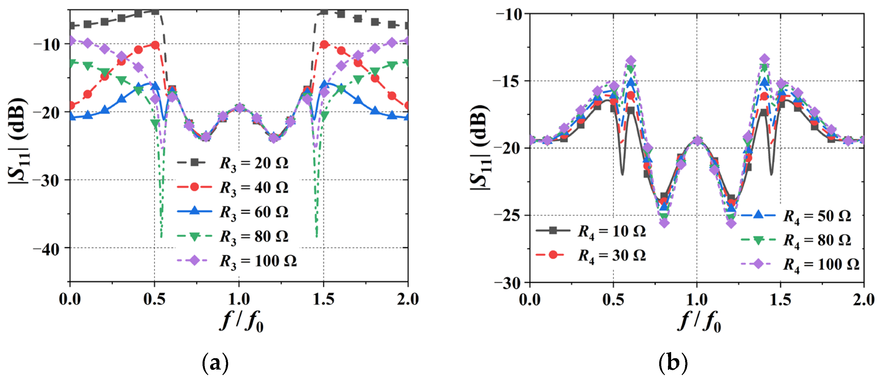
2.2.2. Parametric Analysis

Since stepped open-circuited stubs are connected in parallel at the output ports, two TZs (ftz1 and ftz2) related to f0 can be obtained when the input impedance ZY is equals 0 (corresponds to S21_FPD = 0), as shown in (6).
f tz 1 = 2 f 0 π · arctan Z 1 Z 2 f tz 2 = 2 f 0 f tz 1
From Equation (6), the TZs of the FPD are controlled by the impedance ratio (IR) of the stepped open-circuited stub (Z1/Z2). Figure 3a gives the variation of the TZs and 3 dB bandwidth under different values of IR. It is observed that when IR increases, the two TZs become closer. In addition, the 3 dB FBW is reduced accordingly. For clear illustration, the |S21_FPD| of the FPD is shown in Figure 3b. It is revealed that when the IR changes from 0.6 to 1.45, the TZs shift from 0.465/1.535 f0 to 0.56/2.44 f0, while the corresponding 3 dB FBW narrows from 80% to 70%. In the design, on the basis of achieving the target bandwidth of 80%, the IR of 0.6 is chosen, which corresponds to two TZs located at 0.84 GHz and 3.16 GHz, respectively. Therefore, when Z2 is chosen to be 70 Ω, the value of Z1 can be calculated to be 42 Ω.
When set S11_FPD = 0, according to the method in [25], four transmission poles (TPs) (ftp1, ftp2, ftp3, ftp4) within the passband can be acquired in the frequency range 0–2 f0. Here, the equation of S11_FPD = 0 is a quartic equation. According to the general solutions of the quartic equation, which can be referred to ref. [25], the expression in (7) is derived. It is noted that since the expressions of the TPs are complex, two groups of intermediate variables (o1, o2, o3, o4, x0, x2, x4) are utilized for simplification, as shown in (8) and (9).
f t p 1 = 2 f 0 π arccot ( 1 2 o 1 1 2 o 2 )
f t p 2 = 2 f 0 π arccot ( 1 2 o 1 + 1 2 o 2 )
f t p 3 = 2 f 0 f t p 2
f t p 4 = 2 f 0 f t p 1
where
o 1 = 2 x 2 3 x 4 + o 3 + x 2 2 + 12 x 0 x 4 9 x 4 2 o 3
o 2 = 4 x 2 3 x 4 o 3 x 2 2 + 12 x 0 x 4 9 x 4 2 o 3
o 3 = 2 3 ( x 2 2 + 12 x 0 x 4 ) 3 x 4 ( o 4 + 4 ( x 2 2 + 12 x 0 x 4 ) 3 + o 4 2 ) 1 3
o 4 = 2 x 2 3 72 x 0 x 2 x 4
and
x 0 = Z 2 2 B 2 A b 8
x 2 = ( Z 1 Z 2 B 2 A b Z 2 2 K A b B a 2 Z 1 Z 2 B a A Z 2 2 A A a A b + Z 2 2 B 2 A b + 2 Z 2 2 A B a 2 Z 2 2 A 2 A b ) 8
x 4 = ( Z 1 Z 2 A A a A b + K Z 1 Z 2 A B a A b + Z 1 Z 2 A 2 A b Z 1 Z 2 B 2 A b 2 Z 1 Z 2 A B a ) 8
A = Z e + Z o B = Z e Z o
A a = Z e a + Z o a B a = Z e a Z o a
A b = Z e b + Z o b B b = Z e b Z o b
According to (7)–(9), the TPs varies along with different circuit parameters and are investigated when the IR is set as 0.6. Figure 4a shows the variations with the coupling C of the CL, where C = (ZeZo)/(Ze + Zo). It is seen that there are four TPs between the two TZs when C is within 4.708–6.2 dB. Out of the range, the TPs are reduced to two. Figure 4b gives the detailed |S11_FPD| performance of the FPD. Wider bandwidth under 10 dB return loss can be obtained for C = 5–5.5 dB. Further, it is found that good impedance matching and equally distributed TPs are obtained simultaneously when the coupling is 5.2 dB. Thus, when the value of Zo is chosen as the 50 Ω, the corresponding value of Ze can be obtained as 172 Ω.
Meanwhile, Figure 5a shows the TPs varied with the coupling CT of a-line in the TCL, where CT = (ZeaZoa)/(Zea + Zoa) [24]. It is seen that the in-band TPs change from four to three when the CT exceeds 6.925 dB. As illustrated in Figure 5b, wider bandwidth can be obtained with 10 dB return loss for CT = 5.5–6.5 dB. Wider impedance matching bandwidth with suitable TPs intervals is obtained when CT equals with 6 dB. Thus, Zea can be calculated as 150.3 Ω when Zoa is assigned as 50 Ω. Figure 6 shows the variations of TPs and |S11_FPD| along with the odd-mode impedance of b-line (Zob). Four TPs can be generated when Zob is larger than 35 Ω. But the |S11_FPD| bandwidth is less influenced by the Zob. Since the even-odd mode impedances of the edge and center lines in the TCL satisfy the relation in (4c), the even-mode impedance Zob of the b-line is calculated to be 156 Ω when Zob is selected as 60 Ω.
The remaining parameters are the isolated resistors R1 and R2, which contribute to the output ports matching and isolation. On the basis of the parameters obtained above, the relationship between R1 and R2 can be expressed by using the condition of S22_FPD = S23_FPD = 0, as shown in (10). Figure 7 shows the calculated |S22_FPD| and |S23_FPD| of the FPD as a different R2. It can be observed that as R2 increases, the |S22_FPD| and |S23_FPD| values around the center frequency are decreasing, while both of the values deteriorate near the side frequencies. Finally, under the criterion of |S22_FPD| and |S23_FPD| less than −20 dB, R2 is selected as 150 Ω. According to (10a), the value of R1 is calculated as 15 Ω.
R 1 = 2 B R ( Z S 1 Z S 2 + Z S 2 Z S 7 2 Z S 6 2 ) A R ( Z S 1 Z S 2 + Z S 2 Z S 7 2 Z S 6 2 ) B R Z S 2
A R = ( Z 11 Z Y Z 0 Z Y Z 0 ) ( Z 11 + R 2 ) 2 Z S 4 2 ( Z 11 + R 2 )
B R = ( Z 11 2 Z 13 2 Z Y Z 0 Z 11 Z Y Z 0 ) ( Z 11 + R 2 ) 2 ( Z 11 Z 14 2 + Z 11 Z 34 2 + 2 Z 13 Z 14 Z 34 Z Y Z 0 Z 14 2 Z Y Z 0 ) ( Z 11 + R 2 )

2.3. Analysis of the AFPD

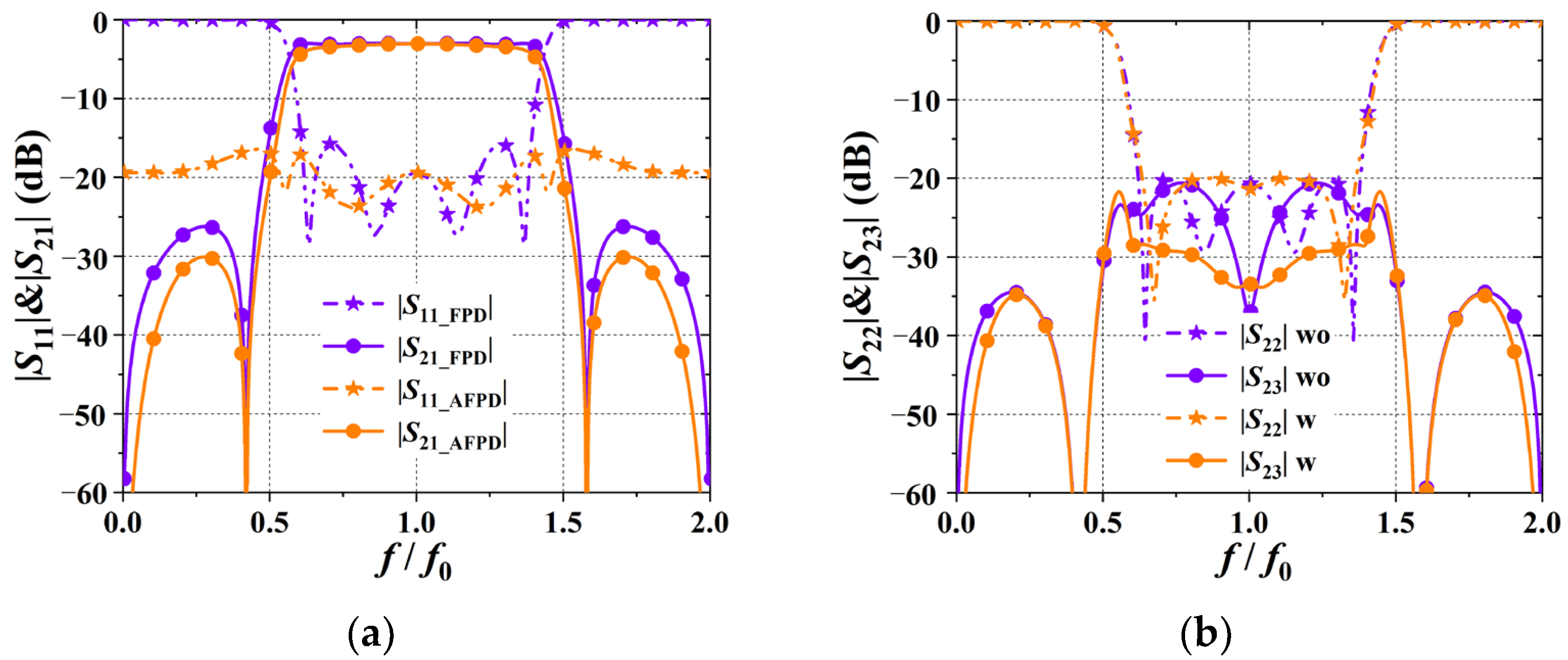
2.3.1. Design Equations and Parametric Analysis

In order to realize the input absorptive characteristic, two absorptive branches are loaded, where the sub-circuits under even-odd mode decomposition method are shown in Figure 8. Then, the overall S-parameters of the AFPD can be denoted as (11).
S 11 _ AFPD = A e _ in Z 0 + B e _ in C e _ in Z 0 2 D e _ in Z 0 A e _ in Z 0 + B e _ in + C e _ in Z 0 2 + D e _ in Z 0
S 21 _ AFPD = S 31 _ AFPD = 2 Z 0 A e _ in Z 0 + B e _ in + C e _ in Z 0 2 + D e _ in Z 0
S 22 _ AFPD = Γ o u t e + Γ o u t o 2
S 23 _ AFPD = Γ o u t e Γ o u t o 2
where
Γ o u t e ( o ) = A e ( o ) _ o u t Z 0 + B e ( o ) _ o u t C e ( o ) _ o u t Z 0 2 D e ( o ) _ o u t Z 0 A e ( o ) _ o u t Z 0 + B e ( o ) _ o u t + C e ( o ) _ o u t Z 0 2 + D e ( o ) _ o u t Z 0
Here, the derivations of Ae_in, Be_in, Ce_in, De_in, and Ae(o)_out, Be(o)_out, Ce(o)_out, De(o)_out in (11) and (12) are shown in Appendix A. According to (11a), the parameters of the absorptive branches can be derived when assigning the absorptive criterion (for example, |S11_AFPD| < −10 dB). Since there are seven unknowns (Z3, Z4, Z5, Z6, Z7, R3, R4) in the absorptive branches, the particle swarm optimization algorithm (PSO) is used for fast computation. Equation (13) lists the defined objective function F. Here, N1 and N2 are the sampling points numbers in the absorptive and filtering bands, respectively. fi is the sample frequency, where the sample interval is f0/D. It is noted that in the function F, g1 is denoted as more than 10 dB at the input absorptive band, which corresponds to L1 = 10 dB. In addition, to guarantee non-deterioration on other performances (output port impedance matching and isolation), the criteria g2 and g3 are added. In (13c) and (13d), the L2 represents the limiting conditions of output port impedance matching and isolation, which equals 20 dB.
F ( Z 3 , Z 4 , Z 5 , Z 6 , Z 7 , R 3 , R 4 ) = g 1 + g 2 + g 3
g 1 = 1 N 1 i = 1 N 1 | | S 11 ( f i ) | 2 10 L 1 10 |
g 2 = 1 N 2 i = 1 N 2 | | S 22 ( f i ) | 2 10 L 2 10 |
g 3 = 1 N 2 i = 1 N 2 | | S 23 ( f i ) | 2 10 L 2 10 |
Figure 9 gives the detailed optimization flow chart. In the design, the sampling interval f0/D is chosen as 0.1 GHz, and the number of sampling points N1 and N2 were selected as 21 and 13, respectively, to cover the absorptive and filtering bands. The impedance range is limited to 40–120 Ω for practical considerations and for quick calculations. Then, the parameters of the absorptive branches can be obtained.
Figure 10 shows the effects of the resistors R3 and R4 on |S11| of the AFPD. It is seen that the out-of-band absorptive feature is mainly influenced by R3. As R3 increases within 20–60 Ω, the out-of-band return loss is increased. When R3 continues to increase from 60 Ω to 100 Ω, the 10 dB absorptive bandwidth is nearly unchanged, only the matching degree is influenced. As can be seen in Figure 10b, the changing of R4 will affect the matching degree of the input port, but the 10 dB absorptive bandwidth is nearly unchanged.

2.3.2. Theory Results and Design Procedures

Table 1 displays the calculated circuit parameters of the AFPD. Based on Table 1, the performance of the AFPD is obtained and listed in Figure 11. For convenience, the S-parameters of FPD and AFPD are compared directly. It is observed from Figure 11a that by inserting the absorptive branches, the bandwidth for 15 dB return loss at the input port is increased from 79% (0.61 f0–1.40 f0) to 200% (0–2 f0). In addition, the out-of-band suppression has been enhanced to over 30 dB. Under the criterion of |S21| = −6 dB, the calculated bandpass bandwidth is 85%, and the RC (|BW20dB/BW3dB|) reaches 1.17. Figure 11b indicates that the output port impedance matching is less affected by the absorptive branches. But the isolation between output ports is enhanced in the filtering band. After inserting the absorptive branches, the calculated |S23| is less than 21 dB from 0–2 f0, while the |S22| is less than −15 dB from 0.61 f0 to 1.39 f0, yielding a bandwidth of 78%.
The design processes of the proposed APFD are concluded as follows for guidance.
(1)
According to the target 3 dB FBW, determine the IR of the stepped open-circuited stub. Then, the value of Z1 can be calculated according to the preassigned Z2 value.
(2)
According to (7)–(9), the appropriate even- and odd-mode impedances of the CLs (Ze and Zo) and TCLs (Zea, Zoa, Zeb, and Zob) can be selected according to the performance of the TPs and |S11_FPD|.
(3)
Based on the relationship between R1 and R2, as shown in (10), the values of R1 and R2 are obtained by considering the |S22_FPD| and |S23_FPD| performance.
(4)
Finally, based on Figure 9, the absorptive branches (Z3, Z4, Z5, Z6, Z7, R3, and R4) can be optimized under the assigned criteria.

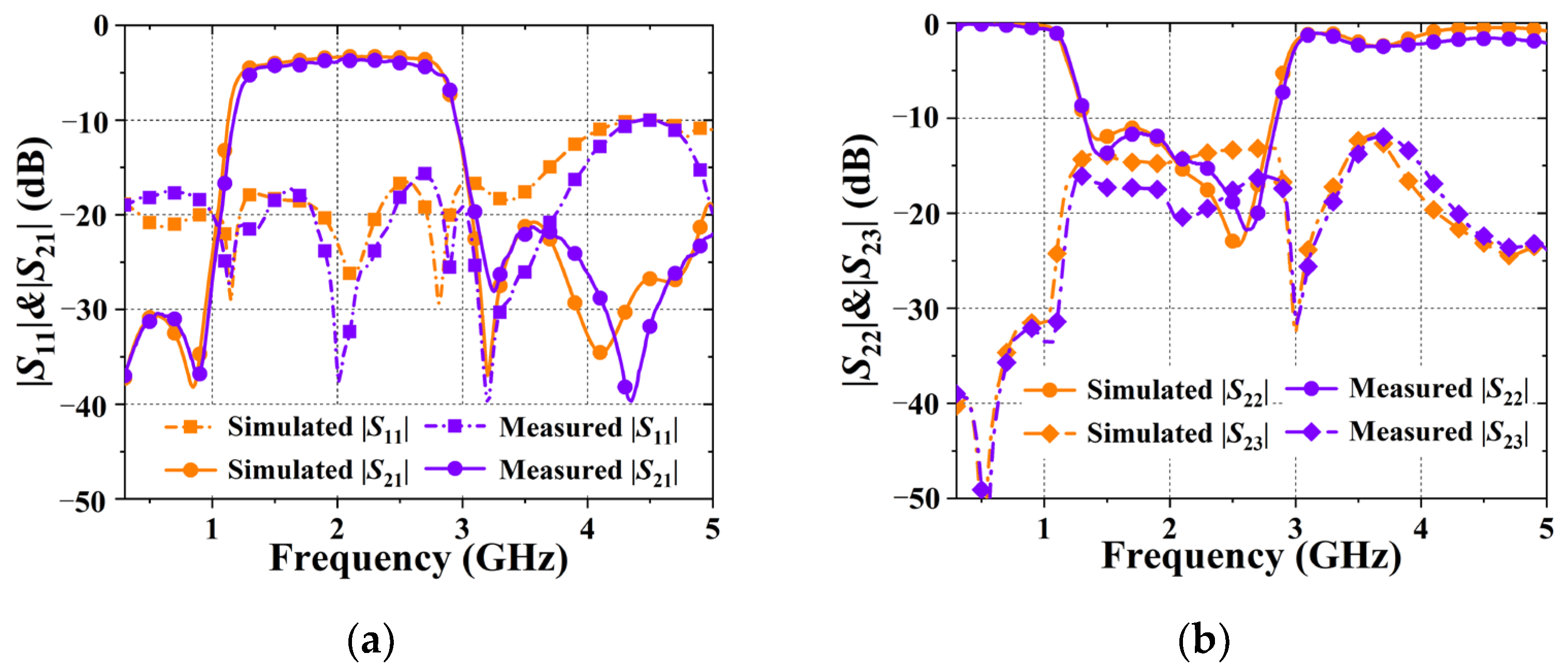
3. Implementation and Measurement

For demonstration, an example is designed at the center frequency of 2 GHz and fabricated on an F4B substrate (εr = 3.5, tanδ = 0.003, and h =1.5 mm). Figure 12 shows the layout and photograph of the fabricated AFPD. The overall dimension of the fabricated prototype is 66 mm × 79 mm, yielding 0.44 λg × 0.53 λgg is the guide wavelength at the center frequency). Table 2 illustrates the final dimensions of the designed AFPD optimized by using the software Ansoft HFSS 13.0. In the process of modeling in the HFSS, the Perfect E boundary is assigned to represent the copper foil in realization. The resistors are represented by the Lumped RLC boundary. In addition, lumped port excitation is applied in the modeling. And the auto mesh method is applied in the simulation, which satisfies high resolution to guarantee accurate results.
The circuit is fabricated through the high-precision corrosion equipment, where the accuracy is 0.01 mm. During the optimization using the HFSS, it is verified that the changing of about 0.01 mm has less effect on the overall performances of the prototype, while the resistors and connectors are soldered by hand. The vector network analyzer (VNA) Agilent N5230A (0.3–25.6 GHz) is used as the test equipment. Firstly, three high-frequency test cables are connected to the port of the VNA. Then, the dedicated calibrator is used to calibrate the three cables simultaneously in the frequency range of 0.3–5 GHz. Finally, connect the three cables to the three ports of the prototype separately and performing the measurement.
Figure 13 shows the simulated and measurement results of the fabricated AFPD, which exhibit great agreements. Firstly, the results between the simulated and theoretical results (Figure 11) are compared. It is found that the curves for the theoretical results are more symmetric and better. This is due to the theory results being based on the equations (obtained from formulas by using the MATLAB), and the field coupling between the structures are not considered. While using the HFSS software to construct the layout, the couplings between the structures for the real layout are taken into consideration. Since the simulated results are influenced by the field coupling between the coupled lines, the bending of the transmission lines, the corner and the connection to the output ports, the layout should be optimized to obtain the best results.
As seen in Figure 13a, the input port of the AFPD is absorptive in the whole measured frequency range, yielding a bandwidth of 250%. In the measurement, at the frequencies of 0.89 GHz and 3.25 GHz, two TZs are observed. Under 3 dB criterion, the passband FBW reaches 82.5% (1.24–2.89 GHz). In addition, the insertion loss (IL) at the center frequency achieved its minimum value of 0.35 dB. It is observed that the insertion loss in simulation is 0.28 dB. This is mainly due to the loss of the substrate, while in measurement, an extra loss of 0.07 dB appears. This may due to the loss induced by the connector or the fabrication error. Under the more strict criterion of 1 dB relative bandwidth, the measured bandwidth is from 1.33 GHz to 2.77 GHz (72%), indicating good passband flatness. In addition, the measured RC is 1.24 and the out-of-band rejection is larger than 20 dB, which indicates good filtering responses. It is observed from Figure 13b that in the absorptive bandwidth, the isolation between the output ports is larger than 12 dB. Under the criterion of 10 dB return loss (RL), the bandwidth for output ports matching reaches 78% (1.22–2.78 GHz).
The performance comparisons between the proposed and representative AFPDs are illustrated in Table 3. In [18,19], the 3 dB BPBW are both less than 20%, and the IL at the center frequency is high. In addition, no output reflection FBW is provided. Compared with the AFPDs in [20,21], which both exhibit more than 50% 3 dB FBW and 200% 10 dB input reflection FBW, the proposed AFPD shows a wider 3 dB BPBW of more than 80%, wider output reflection FBW of more than 70%, and smaller RC of 1.24. The out-of-band suppression of the proposed AFPD is also better than the work in [21]. In addition, in consideration of the 1 dB BPBW and 3 dB BPBF items, it is found that the designed AFPD exhibits more flat output port distributions.

4. Conclusions

In this paper, an AFPD with a wide 3 dB passband bandwidth, wide input absorptive bandwidth, wide 10 dB output reflection bandwidth, high selectivity, deep out-of-band rejection, and flat passband response is proposed. In the measurement, the results indicate that more than 70% bandwidths are achieved for 1 dB passband and 10 dB output reflection. The absorptive bandwidth for the input port reaches 250%. In addition, a minimum passband insertion loss of 0.35 dB is obtained. Due to its simple structure and complete design process, the proposed AFPD can be used as a replacement of the traditional reflective PD for improving the system performance, which has broad application prospects in the modern wideband communication system.

Author Contributions

Conceptualization, H.L. and S.Z.; methodology, H.L. and S.Z.; software, S.C.; validation, Z.W. and S.F.; formal analysis, H.L. and S.Z.; investigation, S.C.; resources, H.L., Z.W. and S.F.; data curation, Z.W. and S.F.; writing—original draft preparation, S.Z.; writing—review and editing, H.L.; visualization, S.C.; supervision, S.Z.; project administration, S.F.; funding acquisition, H.L. and Z.W. All authors have read and agreed to the published version of the manuscript.

Funding

This work was supported in part by the National Natural Science Foundation of China under Grant 51809030, in part by the Liaoning Revitalization Talents Program under Grant XLYC2007067, in part by the Young Elite Scientists Sponsorship Program by CAST under Grant 2022QNRC001, and in part by the Fundamental Research Funds for the Central Universities under Grant 3132023246.

Data Availability Statement

All data are included within the manuscript.

Conflicts of Interest

The authors declare no conflict of interest.

Appendix A

M e _ in = [ A e _ in B e _ in C e _ in D e _ in ] = M A · M T C L · M C L _ A · M Y
Here, the MA, MTCL, MCL_A and MY represent the ABCD matrices of the absorptive branch at the input port, the TCL, the CL with absorptive branch, and the stepped open-circuited stub, respectively, when input from port 1. And Equation (A2) gives the detailed ABCD expressions of MA, MTCL, MCL_A and MY.
M A = [ 1 0 Z 3 + j Z c tan θ Z 3 ( Z c + j Z 3 tan θ ) 1 ]
M T C L = [ Z S 2 Z S 6 Z S 2 ( Z S 1 + Z S 7 ) Z S 6 2 Z S 6 1 Z S 6 Z S 1 + Z S 7 Z S 6 ]
M C L _ A = [ Z 22 ( Z 33 + R e ) Z 23 Z 32 Z 42 ( Z 33 + R e ) Z 43 Z 32 ( Z 22 Z 23 Z 32 Z 33 + R e ) ( Z 44 ( Z 33 + R e ) Z 34 Z 43 Z 42 ( Z 33 + R e ) Z 32 Z 43 ) + Z 34 Z 23 Z 33 + R e Z 24 Z 33 + R e Z 42 ( Z 33 + R e ) Z 43 Z 32 Z 44 ( Z 33 + R e ) Z 34 Z 43 Z 42 ( Z 33 + R e ) Z 32 Z 43 ]
M Y = [ 1 0 j Z 1 + Z 2 Z 2 ( Z 1 cot θ Z 2 tan θ ) 1 ]
where
Z c = Z 4 Z 5 Z 6 cot θ + j R 3 ( Z 4 Z 6 Z 4 Z 5 cot 2 θ ) j ( Z 5 Z 6 + Z 4 Z 6 Z 4 Z 5 cot 2 θ ) + R 3 ( Z 5 cot θ Z 6 tan θ )
R e = R 2 + 2 R 4 + j 2 Z 7 tan θ
When input at port 2 under the even-mode excitation, the corresponding ABCD matrix [Me_out] is listed in (A4).
M e _ o u t = [ A e _ o u t B e _ o u t C e _ o u t D e _ o u t ] = M Y · M C L _ A 1 · M T C L 1 · M A
where
M T C L 1 = [ Z S 1 + Z S 7 2 Z S 6 Z S 2 ( Z S 1 + Z S 7 ) 2 Z S 6 Z S 6 1 2 Z S 6 Z S 2 2 Z S 6 ]
M C L _ A 1 = [ Z 44 ( Z 33 + R e ) Z 43 Z 34 Z 24 ( Z 33 + R e ) Z 23 Z 34 ( Z 44 Z 43 Z 34 Z 33 + R e ) ( Z 22 ( Z 33 + R e ) Z 32 Z 23 Z 24 ( Z 33 + R e ) Z 34 Z 23 ) + Z 32 Z 43 Z 33 + R e Z 42 Z 33 + R e Z 24 ( Z 33 + R e ) Z 23 Z 34 Z 22 ( Z 33 + R e ) Z 32 Z 23 Z 24 ( Z 33 + R e ) Z 34 Z 23 ]
Here, MTCL1 and MCL_A1 are the ABCD matrices of the TCL and the absorptive-branch-loaded CL, respectively, when input from port 2. Based on Figure 8b, the ABCD matrix [Mo_out] between ports 2 and 3 under odd-mode excitation is shown in (A6). It is noted that the MTCL_S is defined as the ABCD matrix of the TCL with center-line shorted. Let MCL_R1 and MCL_R represent the ABCD matrices of the absorptive-branch-loaded CL connected to port 2 and 3, respectively. M1 is the ABCD matrix of the resistor R1/2.
M o _ o u t = [ A o _ o u t B o _ o u t C o _ o u t D o _ o u t ] = ( M Y · M C L _ R 1 · M 1 · M T C L _ S · M 1 · M C L _ R · M Y )
where
M C L _ R = [ Z 22 ( Z 33 + R 2 ) Z 23 Z 32 Z 42 ( Z 33 + R 2 ) Z 43 Z 32 ( Z 22 Z 23 Z 32 Z 33 + R 2 ) ( Z 44 ( Z 33 + R 2 ) Z 34 Z 43 Z 42 ( Z 33 + R 2 ) Z 32 Z 43 ) + Z 34 Z 23 Z 33 + R 2 Z 24 Z 33 + R 2 Z 42 ( Z 33 + R 2 ) Z 43 Z 32 Z 44 ( Z 33 + R 2 ) Z 34 Z 43 Z 42 ( Z 33 + R 2 ) Z 32 Z 43 ]
M C L _ R 1 = [ Z 44 ( Z 33 + R 2 ) Z 34 Z 43 Z 24 ( Z 33 + R 2 ) Z 34 Z 23 ( Z 44 Z 43 Z 34 Z 33 + R 2 ) ( Z 22 ( Z 33 + R 2 ) Z 23 Z 32 Z 24 ( Z 33 + R 2 ) Z 23 Z 34 ) + Z 34 Z 23 Z 33 + R 2 Z 24 Z 33 + R 2 Z 24 ( Z 33 + R 2 ) Z 23 Z 34 Z 22 ( Z 33 + R 2 ) Z 23 Z 32 Z 24 ( Z 33 + R 2 ) Z 23 Z 34 ]
M T C L _ S = [ Z S 1 Z S 2 Z S 6 2 Z S 2 Z S 7 Z S 6 2 ( Z S 1 Z S 6 2 Z S 2 ) ( Z S 1 Z S 2 Z S 6 2 Z S 2 Z S 7 Z S 6 2 ) + Z S 6 2 Z S 2 Z S 7 Z S 2 Z S 2 Z S 7 Z S 6 2 Z S 1 Z S 2 Z S 6 2 Z S 2 Z S 7 Z S 6 2 ]
M 1 = [ 1 0 2 R 1 1 ]

References

  1. Chen, M.-T.; Tang, C.-W. Design of the filtering power divider with a wide passband and stopband. IEEE Microw. Wirel. Compon. Lett. 2018, 28, 570–572. [Google Scholar] [CrossRef]
  2. Yu, X.; Sun, S. A novel wideband filtering power divider with embedding three-line coupled structures. IEEE Access 2018, 6, 41280–41290. [Google Scholar] [CrossRef]
  3. Wang, X.; Wang, J.; Zhang, G.; Hong, J.-S.; Wu, W. Dual-wideband filtering power divider with good isolation and high selectivity. IEEE Microw. Wirel. Compon. Lett. 2017, 27, 1071–1073. [Google Scholar] [CrossRef]
  4. Zhang, G.; Wang, J.; Zhu, L.; Wu, W. Dual-band filtering power divider with high selectivity and good isolation. IEEE Microw. Wirel. Compon. Lett. 2016, 26, 774–776. [Google Scholar] [CrossRef]
  5. Wang, X.; Wang, J.; Choi, W.-W.; Yang, L.; Wu, W. Dual-wideband filtering power divider based on coupled stepped-impedance resonators. IEEE Microw. Wirel. Compon. Lett. 2018, 28, 873–875. [Google Scholar] [CrossRef]
  6. Zhang, G.; Qian, Z.; Yang, J.; Hong, J.-S. Wideband four-way filtering power divider with sharp selectivity and high isolation using coshared multi-mode resonators. IEEE Microw. Wirel. Compon. Lett. 2019, 29, 641–644. [Google Scholar] [CrossRef]
  7. Zhu, H.; Abbosh, A.M.; Guo, L. Wideband four-way filtering power divider with sharp selectivity and wide stopband using looped coupled-line structures. IEEE Microw. Wirel. Compon. Lett. 2016, 26, 413–415. [Google Scholar] [CrossRef]
  8. Zhu, C.; Zhang, J. Design of high-selectivity asymmetric three-way equal wideband filtering power divider. IEEE Access 2019, 7, 55329–55335. [Google Scholar] [CrossRef]
  9. Zhao, X.; Song, K.; Zhu, Y.; Fan, Y. Wideband four-way filtering power divider with isolation performance using three parallel-coupled lines. IEEE Microw. Wirel. Compon. Lett. 2017, 27, 800–802. [Google Scholar] [CrossRef]
  10. Psychogiou, D.; Gómez-García, R.; Guyette, A.C.; Peroulis, D. Reconfigurable single/multi-band filtering power divider based on quasi-bandpass sections. IEEE Microw. Wirel. Compon. Lett. 2016, 26, 684–686. [Google Scholar] [CrossRef]
  11. Yahya, S.I.; Alameri, B.M.; Jamshidi, M.; Roshani, S.; Chaudhary, M.A.; Ijemaru, G.K.; Mezaal, Y.S.; Roshani, S. A New Design Method for Class-E Power Amplifiers Using Artificial Intelligence Modeling for Wireless Power Transfer Applications. Electronics 2022, 11, 3608. [Google Scholar] [CrossRef]
  12. Jamshidi, M.; Yahya, S.I.; Nouri, L.; Hashemi-Dezaki, H.; Rezaei, A.; Chaudhary, M.A. A Super-Efficient GSM Triplexer for 5G-Enabled IoT in Sustainable Smart Grid Edge Computing and the Metaverse. Sensors 2023, 23, 3775. [Google Scholar] [CrossRef] [PubMed]
  13. Lee, J.; Lee, B.; Nam, S.; Lee, J. Rigorous design method for symmetric reflectionless filters with arbitrary prescribed transmission response. IEEE Trans. Microw. Theory Techn. 2020, 68, 2300–2307. [Google Scholar] [CrossRef]
  14. Fan, M.; Song, K.; Yang, L.; Gómez-García, R. Frequency-tunable constant-absolute-bandwidth single-/dual-passband filters and diplexers with all-port-reflectionless behavior. IEEE Trans. Microw. Theory Techn. 2021, 69, 1365–1377. [Google Scholar] [CrossRef]
  15. Gómez-García, R.; Muñoz-Ferreras, J.; Psychogiou, D. Symmetrical quasi-absorptive RF bandpass filters. IEEE Trans. Microw. Theory Techn. 2019, 67, 1472–1482. [Google Scholar] [CrossRef]
  16. Wu, X.; Li, Y.; Liu, X. Quasi-reflectionless microstrip bandpass filters with improved passband flatness and out-of-band rejection. IEEE Access 2020, 8, 160500–160514. [Google Scholar] [CrossRef]
  17. Xu, K.-D.; Lu, S.; Guo, Y.-J.; Chen, Q. Quasi- reflectionless filters using simple coupled line and t-shaped microstrip structures. IEEE J. Radio Freq. Identif. 2020, 6, 54–63. [Google Scholar] [CrossRef]
  18. Gómez-García, R.; Muñoz-Ferreras, J.-M.; Psychogiou, D. RF reflectionless filtering power dividers. IEEE Trans. Circuits Syst. II Exp. Briefs 2019, 66, 933–937. [Google Scholar] [CrossRef]
  19. Fan, M.; Song, K.; Yang, L.; Gómez-Garcia, R. Frequency-reconfigurable input-reflectionless bandpass filter and filtering power divider with constant absolute bandwidth. IEEE Trans. Circuits Syst. II Exp. Briefs 2021, 68, 2424–2428. [Google Scholar] [CrossRef]
  20. Zhang, Y.; Wu, Y.; Yan, J.; Wang, W. Wideband high-selectivity filtering all-frequency absorptive power divider with deep out-of-band suppression. IEEE Trans. Plasma Sci. 2021, 49, 2099–2106. [Google Scholar] [CrossRef]
  21. Zhu, Y.-H.; Cai, J.; Cao, Y.; Chen, J.-X. Compact wideband absorptive filtering power divider with a reused composite T-Shape network. IEEE Trans. Circuits Syst. II Exp. Briefs 2023, 70, 899–903. [Google Scholar] [CrossRef]
  22. Zysman, G.I.; Johnson, A.K. Coupled Transmission Line Networks in an Inhomogeneous Dielectric Medium. IEEE Trans. Microw. Theory Techn. 1969, 17, 753–759. [Google Scholar] [CrossRef]
  23. Ozaki, H.; Ishii, J. Synthesis of a Class of Strip-Line Filters. IRE Trans. Circuit Theory 1958, 5, 104–109. [Google Scholar] [CrossRef]
  24. Chen, C.P.; Kato, N.; Anada, T. Synthesis scheme for wideband filters consisting of three-coupled-lines including the cross coupling between non-adjacent lines. IET Microw. Antennas Propag. 2015, 9, 1558–1566. [Google Scholar] [CrossRef]
  25. Wu, Y.; Cui, L.; Zhuang, Z.; Wang, W.; Liu, Y. A simple planar dual-band bandpass filter with multiple transmission poles and zeros. IEEE Trans. Circuits Syst. II Exp. Briefs 2018, 65, 56–60. [Google Scholar] [CrossRef]
Figure 1. Circuit topology of the proposed AFPD.
Electronics 12 03704 g001
Figure 2. The (a) even- and (b) odd-mode sub-circuits of the FPD.
Electronics 12 03704 g002
Figure 3. Calculated performances of the FPD with different IRs. (a) TZs and 3 dB FBW. (b) |S21_FPD|.
Electronics 12 03704 g003
Figure 4. Calculated (a) TPs and (b) |S11_FPD| of the FPD under different C when Zo is chosen as 50 Ω. (Z1 = 42 Ω, Z2 = 70 Ω).
Electronics 12 03704 g004
Figure 5. Calculated (a) TPs and (b) |S11_FPD| of the FPD with different CT when Zoa is chosen as 50 Ω. (Z1 = 42 Ω, Z2 = 70 Ω, Ze = 172 Ω, Zo = 50 Ω).
Electronics 12 03704 g005
Figure 6. Calculated (a) TPs and (b) |S11_FPD| of the FPD with different Zob. (Z1 = 42 Ω, Z2 = 70 Ω, Ze = 172 Ω, Zo = 50 Ω, Zea = 150 Ω, Zoa = 50 Ω).
Electronics 12 03704 g006
Figure 7. Calculated (a) |S22_FPD| and (b) |S23_FPD| of the FPD with different R2. (Z1 = 42 Ω, Z2 = 70 Ω, Ze = 172 Ω, Zo = 50 Ω, Zea = 150 Ω, Zoa = 50 Ω, Zeb = 156 Ω, Zob = 60 Ω).
Electronics 12 03704 g007
Figure 8. Equivalent (a) even- and (b) odd-mode sub-circuits of the AFPD.
Electronics 12 03704 g008
Figure 9. The optimization flowchart.
Electronics 12 03704 g009
Figure 10. Effects of (a) R3 and (b) R4 on |S11| of the AFPD.
Electronics 12 03704 g010
Figure 11. Theory results of the AFPD and FPD. (a) |S11| and |S21|, (b) |S22| and |S23|.
Electronics 12 03704 g011
Figure 12. Layout and photograph of the fabricated AFPD.
Electronics 12 03704 g012
Figure 13. The simulated and measured results of the fabricated AFPD. (a) |S11| and |S21|, (b) |S22| and |S23|.
Electronics 12 03704 g013
Table 1. Calculated values of the AFPD.
Z1 (Ω)Z2 (Ω)Z3 (Ω)Z4 (Ω)Z5 (Ω)Z6 (Ω)Z7 (Ω)Ze (Ω)θ (°)
427010252.91204012017290
Zo (Ω)Zea (Ω)Zoa (Ω)Zeb (Ω)Zob (Ω)R1 (Ω)R2 (Ω)R3 (Ω)R4 (Ω)
50150.35015660151506211
Table 2. Final dimensions of the AFPD (Unit: mm).
WtLtW1L1W2L2_1L2_2W3L3W4L4
3.314.55.122.2326.2419.260.6528.93.0421.8
W5L5_1L5_2W6L6_1L6_2W7L7_1L7_2L7_3L7_4
0.33204.24.54129.80.4432.43.27.4
L7_5L7_6WeLeSeLSWSWaWbWdr
2.43.10.5121.80.223.40.240.590.491.51.5
R1R2R3R4
15 Ω150 Ω50 Ω13 Ω
Table 3. Performance Comparisons Between the Proposed and Representative AFPDs.
Test Band
(GHz)
1 dB BPBW
(%)
3 dB BPBW
(%)
10 dB IRFBW
(%)
10 dB ORFBW
(%)
Out-of-Band Rejection (dB)RCIL a (dB)
[18]1–37.4 *13.675.5 *->152.88 *0.9
[19]0.5–29.1 *11.6 *87->231.42 *2.5
[20]0–525.9 *51.4 *28562.3>301.56 *0.9
[21]0–552.8-21242.4>171.45 *0.32
This work0–57282.525078>201.240.35
BPBW: Passband bandwidth based on |S21|. IRFBW: Input reflection FBW. ORFBW: Output reflection FBW. RC = rectangular coefficient = |BW20 dB/BW3dB|. a: Minimum passband IL. *: Estimated from the results.
Disclaimer/Publisher’s Note: The statements, opinions and data contained in all publications are solely those of the individual author(s) and contributor(s) and not of MDPI and/or the editor(s). MDPI and/or the editor(s) disclaim responsibility for any injury to people or property resulting from any ideas, methods, instructions or products referred to in the content.

