Article

A Novel 4H-SiC Double Trench MOSFET with Built-In MOS Channel Diode for Improved Switching Performance

Department of Electronic Engineering, Sogang University, Seoul 04107, Republic of Korea
*
Author to whom correspondence should be addressed.
Electronics 2023, 12(1), 92; https://doi.org/10.3390/electronics12010092
Submission received: 28 October 2022 / Revised: 8 December 2022 / Accepted: 23 December 2022 / Published: 26 December 2022
(This article belongs to the Special Issue Wide Bandgap Semiconductor: From Epilayer to Devices)

Abstract

:
This study proposed a novel 4H-SiC double trench metal-oxide-semiconductor field-effect-transistor (DTMCD-MOSFET) structure with a built-in MOS channel diode. Further, its characteristics were analyzed using TCAD simulation. The DTMCD-MOSFET comprised active and dummy gates that were divided horizontally; the channel diode operated through the dummy gate and the p-base and N+ source regions at the bottom of the dummy gate. Because the bult-in channel diode was positioned at the bottom, the DTMCD-MOSEFT minimized static deterioration. Despite having a 5.2% higher specific on-resistance (Ron-sp) than a double-trench MOSFET (DT-MOSFET), the DTMCD-MOSFET exhibited a significantly superior body diode and switching properties. In comparison to the DT-MOSFET, its turn-on voltage (VF) and reverse recovery charge (Qrr) were decreased by 27.2 and 30.2%, respectively, and the parasitic gate-drain capacitance (Crss) was improved by 89.4%. Thus, compared with the DT-MOSFET, the total switching energy loss (Etot) was reduced by 41.4%.

1. Introduction

Wide-bandgap materials have a higher critical electric field and higher electron velocity than silicon, making them suitable for use in high-voltage and high-speed power MOSFETs [1,2]. In particular, silicon carbide (SiC) has high thermal conductivity and can be used stably at high temperatures; thus, SiC MOSFETs have been evaluated as substitutes for Si IGBTs [3]. SiC MOSFETs primarily fall into two categories: trench-structured UMOSFETs and planar diffusion MOSFETs (DMOSFETs). By lowering the cell pitch, UMOSFETs can enhance the cell density per unit area, while decreasing the JFET area through the gate trench. However, their trench structure renders them susceptible to electric fields [4]. A double-trench MOSFET (DT-MOSFET) and a gate P+ shielding construction have been proposed as solutions to this issue [5,6]. The gate and source trench configuration of the DT-MOSFET facilitates the distribution of the electric field in the gate trench, and the bottom P+ shielding region (BPR) protects the gate oxide from high drain voltages. In addition, attempts have been made to reduce the switching loss of SiC power devices. The decrease in switching time has been investigated as a way to decrease switching loss. Further, a split-gate configuration has been proposed to shorten the switching times, because the gate-drain capacitance (Cgd) is correlated with the switching time [7]. This minimizes the gate-drain overlap region by separating the gate region, thereby reducing Cgd and the switching time and loss. Moreover, the introduction of BPR not only protects the gate oxide, but also reduces Cgd by preventing a coupling effect between the gate and the drain [8].
Reducing the circuit’s antiparallel diode reverse recovery charge is another method for lowering the switching loss. The reverse recovery charge is lower for the SiC Schottky barrier diode (SBD) than for the PiN diode because it functions as a unipolar device with fewer minority carriers still present in the N-drift [9]. Consequently, SiC SBDs are now frequently employed as antiparallel diodes in power circuits. Additionally, considerable research has been conducted on the built-in SBD-MOSFET, which shrinks the size of the power module system and prevents parasitic components of the inductance via the integration of an external SBD inside the MOSFET [10,11,12]. However, there is a barrier lowering owing to the image charge force in the Schottky contact, which can result in a large leakage current when the MOSFET is off due to thermionic field emissions at the lowered barrier, as well as low short-circuit withstand characteristics [13,14].
Another option for lowering the switching loss is a built-in MOS channel diode MOSFET (MCD-MOSFET), which incorporates a channel diode into the MOSFET [15,16,17]. In a typical MOSFET construction, an MCD-MOSFET comprises a source-contacted dummy gate and an active gate that contacts the gate. A channel is established in the P-base region beyond the gate oxide film when a diode turn-on voltage is applied to the dummy gate, which is in contact with the source. Consequently, electrons pass from the drain to the source, resulting in a diode current flow. MCD-MOSFETs have a higher short-circuit withstanding ability and nearly no off-state leakage current problems caused by interface characteristics compared with SBD-MOSFETs. However, when the MCD-MOSFET is in the operating state of a MOSFET rather than a diode, the channel is not activated in the P-base region next to the divided dummy gate that is in contact with the source. This increases the channel resistance and the specific on-resistance. In addition, owing to the electric field crowding effect, a strong electric field is delivered to the gate oxide edge produced by the split-gate construction, which reduces the dependability of the gate dielectric oxide [18,19,20,21].
In this study, a novel double-trench MOSFET (DTMCD-MOSFET) structure was pro-posed, and a TCAD simulator was used to analyze its electrical properties. The DTMCD-MOSFET has a source-contacted dummy gate at the bottom of the active gate, and the BPR consists of a P+ shielding region, an N+ source, and a P-base channel. The channel diode operates through the BPR part. Thus, the DTMCD-MOSFET can utilize the P-base area on both sides during the on state, and a reduction in the channel resistance is prevented. Consequently, the DTMCD-MOSFET offers the benefit of utilizing an internal channel diode to reduce the switching power losses while minimizing the deterioration of the MOSFET’s static properties.

2. Device Structures and Proposed Fabrication Procedures

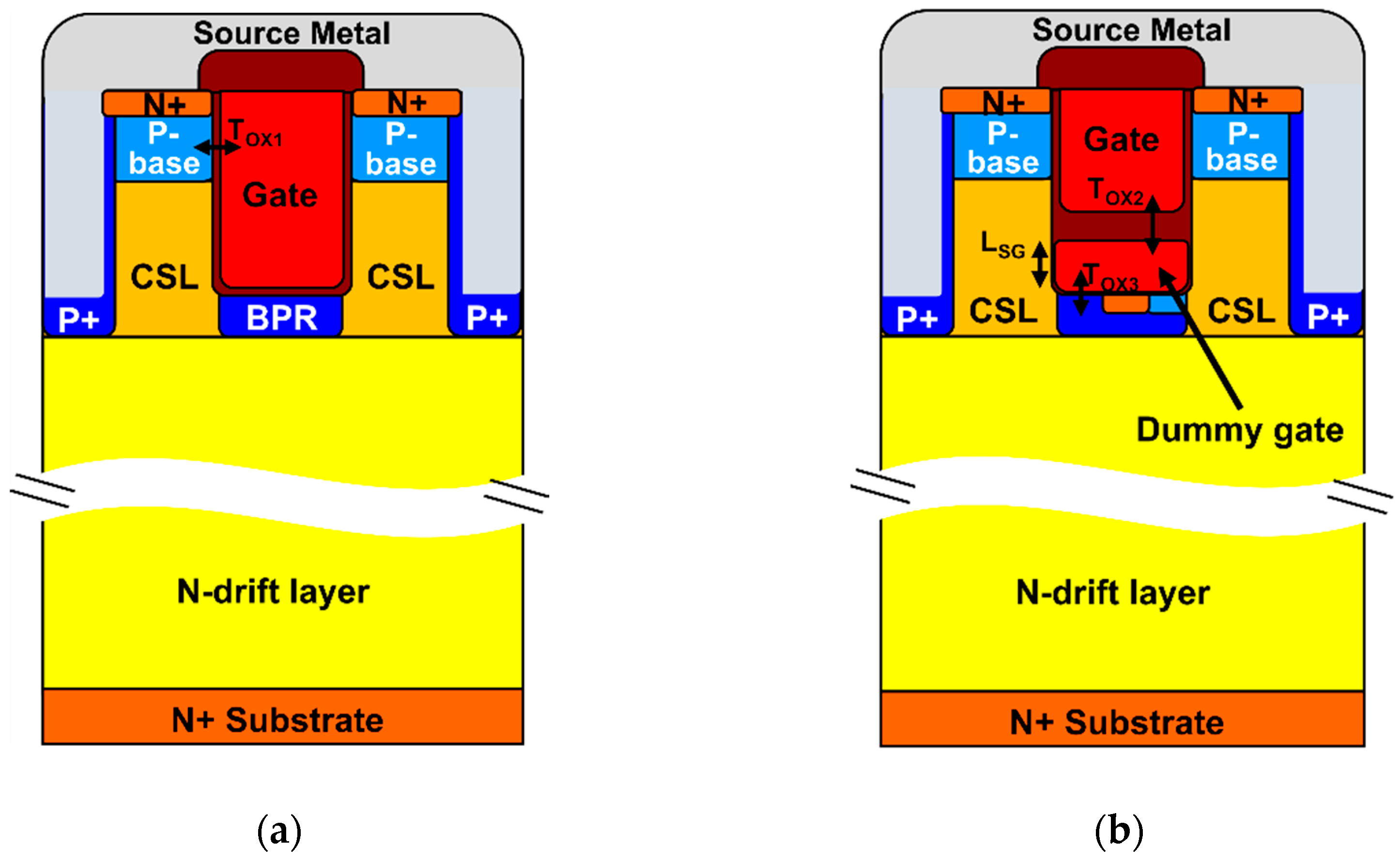
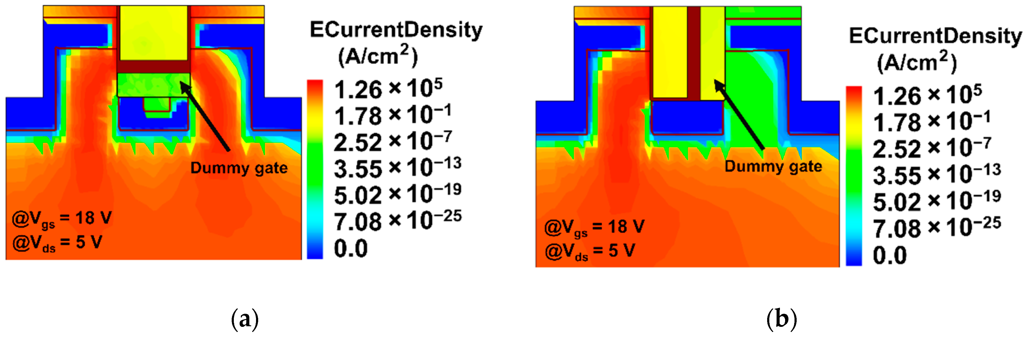
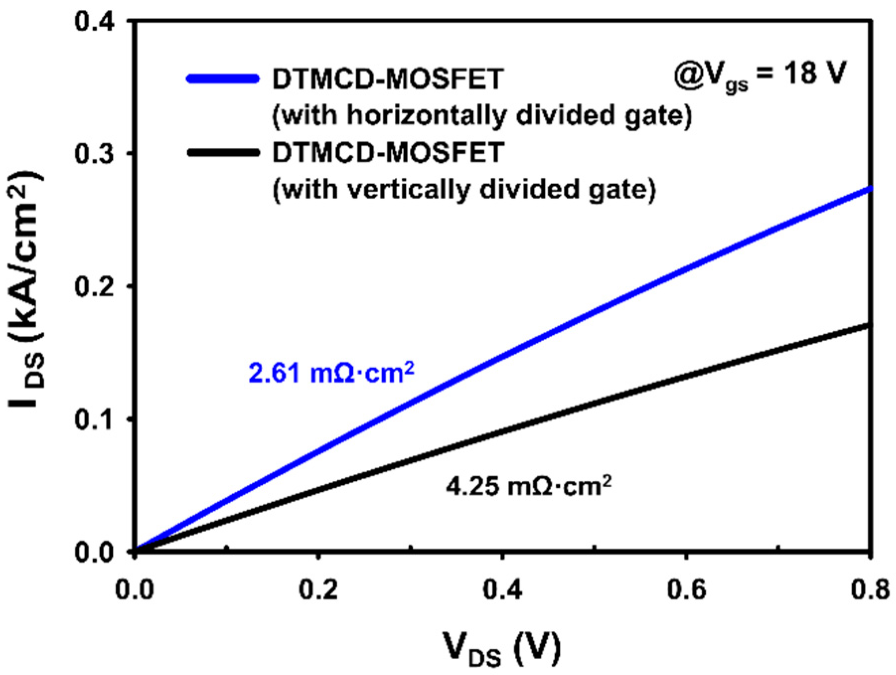
2.1. Device Structures and Optimization

A standard double-trench MOSFET (DT-MOSFET) with BPR and the proposed DTMCD-MOSFET are depicted in the cross-sectional view in Figure 1 [8,22]. The suggested DTMCD-MOSFET is such that the gate is divided horizontally from the current DT-MOSFET, and the source is connected to the dummy gate at the bottom. In addition, the DTMCD-MOSFET features an N+ source and a P-base region in the bottom P+ shielding region (BPR). When a DTMCD-MOSFET is employed as a free-wheeling diode in the switching-off state, the source bias of the dummy gate increases than the drain bias, and the increased bias creates a channel in the P-base region at the BPR. Consequently, the channel diode is activated, generating a current flow from the N+ source at the BPR to the drain. Apart from a few minor differences, the device parameters of the DT-MOSFET and the DTMCD-MOSFET are basically the same. The doping concentrations of N-drift and CSL are 7 × 1015 cm−3 and 2 × 1015 cm−3, respectively. Also, the doping concentration of the P-base and P+ shielding region are 2 × 1017 cm−3 and 2 × 1018 cm−3, respectively. As for the length parameters, the gate and source trench depths of both devices are 1.5 µm, the N-drift length is 10 µm, and the cell pitch is 4.8 µm. For both devices, the active gate oxide (Tox1) thickness is 50 nm. Only the DTMCD-MOSFET has the length parameters Tox2, Tox3, and LSG; Tox2 was set to 210 nm, Tox3 to 10 nm, and LSG was set to 0.4 µm. The device parameters for the DT-MOSFET and the DTMCD-MOSFET are summarized in Table 1.
According to the split dummy gate length LSG, Figure 2 depicts the DTMCD-MOSFET’s optimization features. The active gate length decreased as the LSG increased, which resulted in a reduction in the gate-drain coupling effect and a consequent decrease in the parasitic gate-drain capacitance (Cgd). However, because of the shorter active gate length, the accumulation layer declined, increasing the specific on-resistance (Ron-sp) [23]. In this case, the high-frequency figure-of-merit (H-FOM; H-FOM = Ron-sp × Cgd) can be used to determine the optimal point [24]. Owing to the possibility of reducing the conduction and switching losses with a decrease in the Ron-sp and Cgd, the point with the smallest H-FOM value is the optimal device, and it was obtained when LSG = 0.4 µm.
In contrast to the DT-MOSFET, the DTMCD-MOSFET undergoes two thermal oxidation stages. In the gate trench region, the first oxidation yielded 10 nm Tox1 and 10 nm Tox3, whereas the second oxidation, which proceeded after dummy gate deposition, yielded the remaining Tox1 and Tox2. Owing to the fact that the oxidation rate of polysilicon is higher than that of silicon carbide, Tox2 grew thicker than Tox1 [25,26,27]. Wet thermal oxidation with H2O was conducted using Sentaurus process simulation at 1215 °C, resulting in the formation of 210 nm of Tox2 and 50 nm of Tox1. The following subsection provides additional information on the proposed fabrication process sequence for the DTMCD-MOSFET.

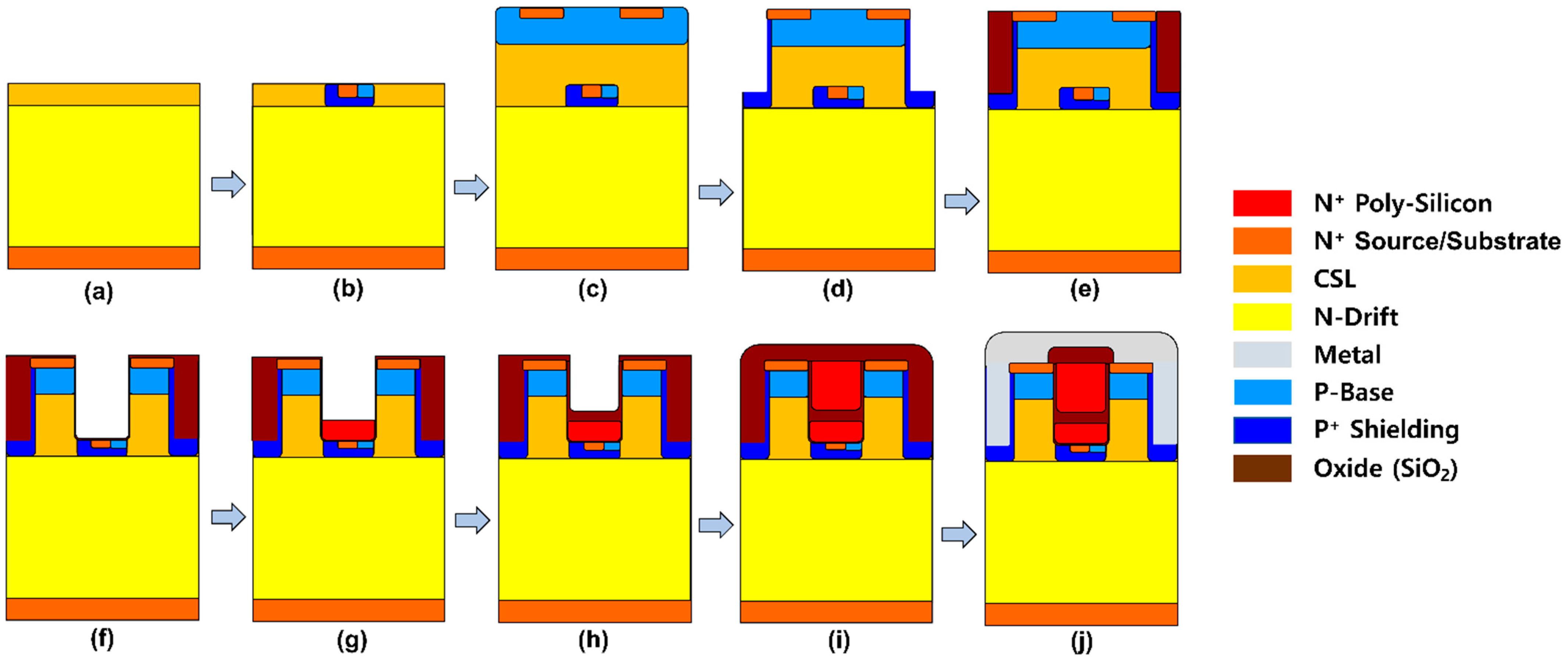
2.2. Proposed Fabrication Procedures

Figure 3 shows the proposed fabrication process flowchart of the DTMCD-MOSFET. First, the N-drift and current spread layer (CSL) regions were formed through a 4° off-axis epitaxial growth (Figure 3a) [28]. Ion implantation was then used to create the BPR region, which consists of the P+ shielding, P-base, and N+ source regions of the channel diode gate (Figure 3b) [29]. In Figure 3c, the remaining CSL and P-base regions were created through epitaxial growth, and N+ source regions were subsequently created through ion implantation [30]. The source trench and side P+ shielding shown in Figure 3d were created using RIE-ICP etching and tilt-ion implantation [31]. Subsequently, the source region was filled using oxide deposition, as shown in Figure 3e, and the gate trench was created using etching, as shown in Figure 3f, followed by wet thermal oxidation to form Tox3 [32]. In addition, N+-doped polysilicon was deposited and etched to create the dummy gate shown in Figure 3g, and wet thermal oxidation was used once again to create Tox1 and Tox2 in Figure 3h [33,34,35]. As shown in Figure 3i, an active gate was formed through polysilicon deposition and etch-back processes, followed by oxide deposition [36]. Finally, the oxide was etched to form an ILD oxide, and the deposition of the source metal completed the discrete MCD-MOSFET device process (Figure 3j).

3. Simulation Results and Discussions

In this section, we present and analyze the simulation results for the electrical characteristics of the proposed and compared devices. The simulation was performed using the Sentaurus TCAD tool from Synopsys, and Poisson’s equations and the electron/hole continuity equations were solved in a two-dimensional (2D) MOSFET structure [37]. For the simulation conditions, physical models, such as the mobility, recombination, generation, and avalanche models, and the density of the interface states at the SiC/SiO2 interface, were performed under the same conditions as in our previous study [18]. Through simulations, the static performance of the MOSFETs in their on and off states, the body diode properties of the MOSFETs, and their dynamic performance, including their parasitic capacitance and switching characteristics, were compared. Furthermore, the reverse recovery, capacitance, and switching characteristics were simulated using the circuit configuration of the mixed-mode simulation.

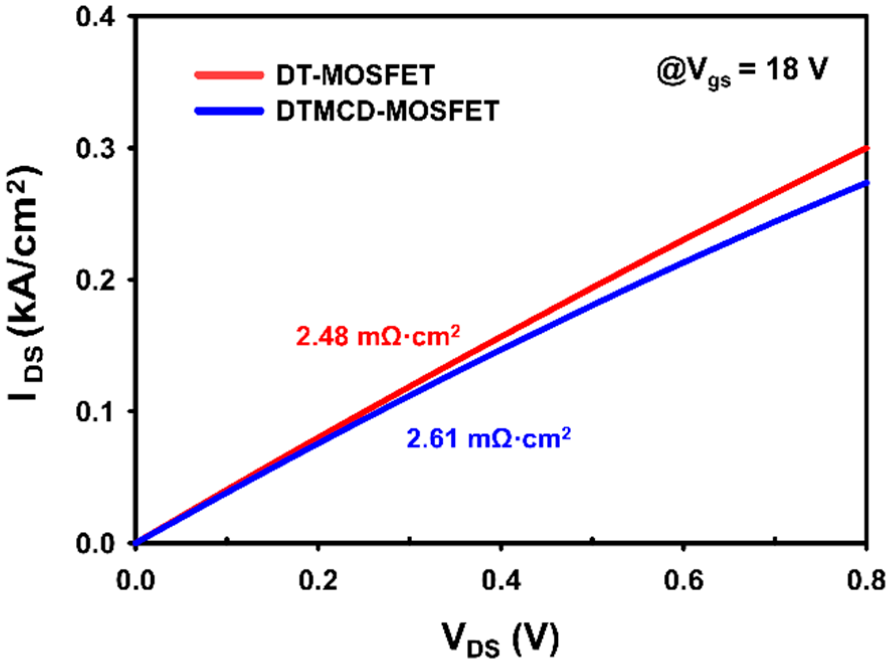
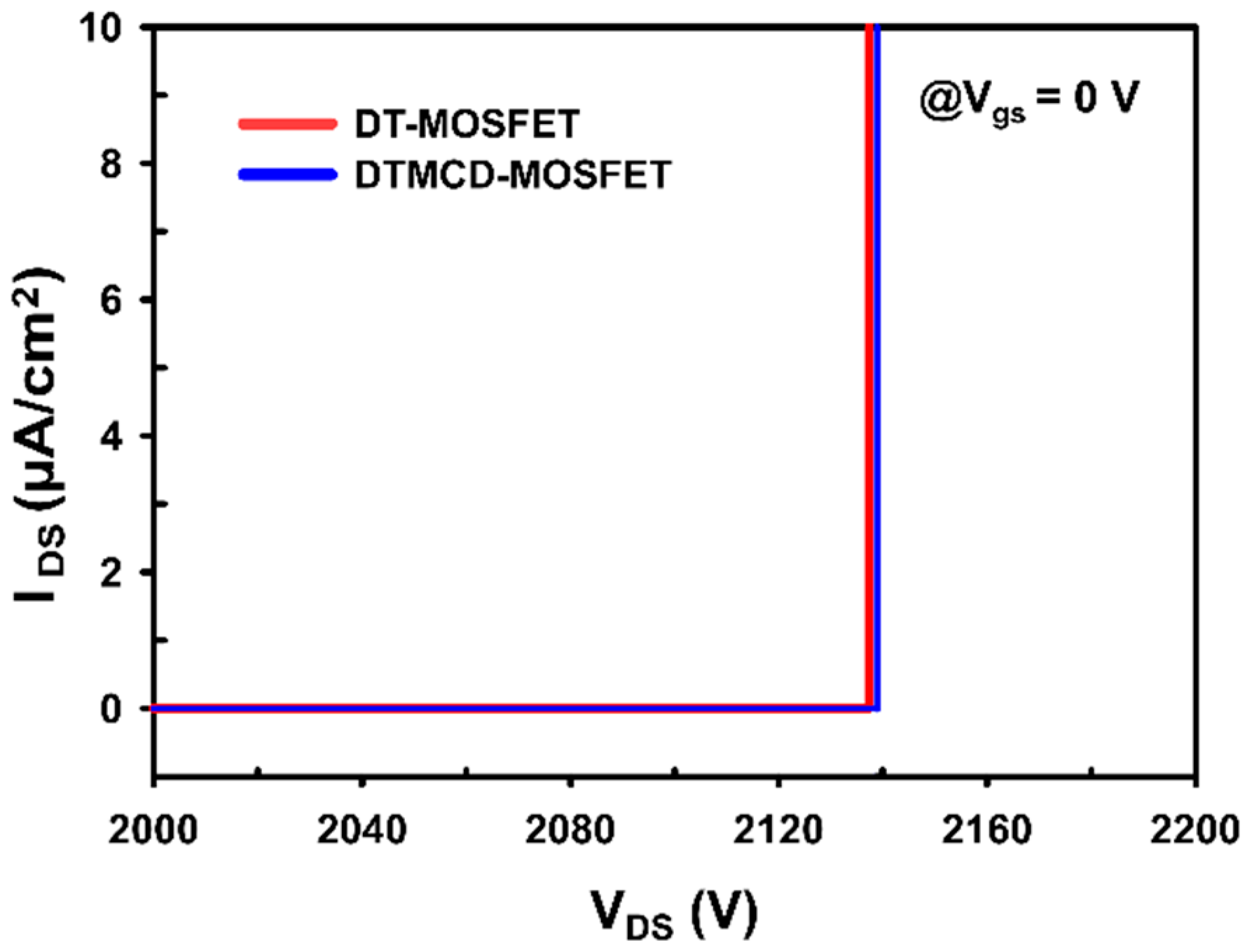
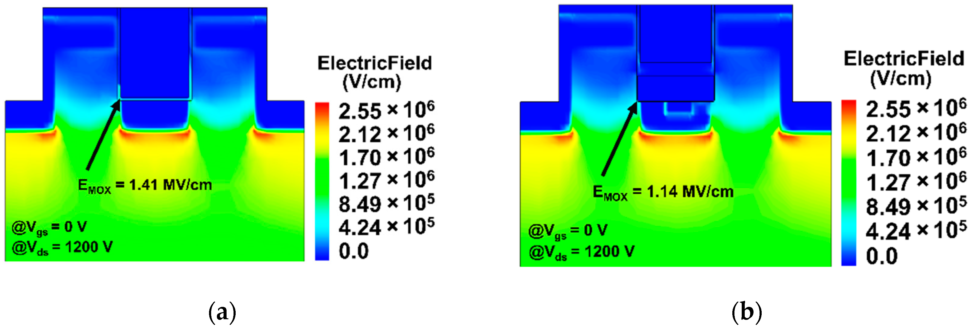
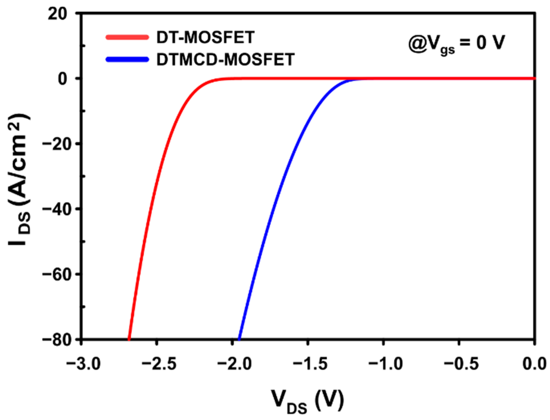
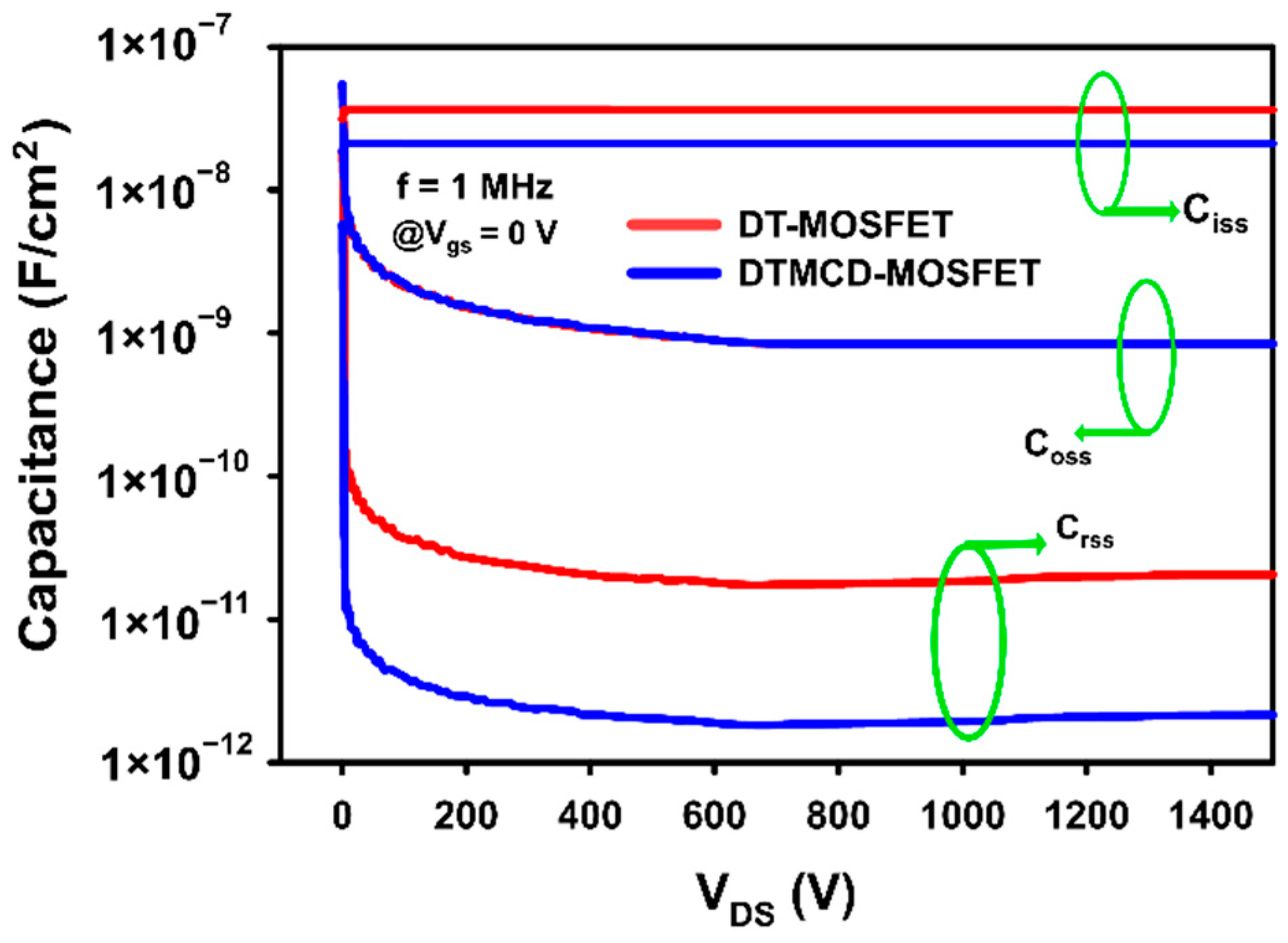
3.1. Static Performances

Figure 4 depicts the drain current characteristics versus the drain voltage of the DT-MOSFET and DTMCD-MOSFET properties in the on state. Because of the reduced accumulation layer caused by the split-gate construction, the Ron-sp of the DTMCD-MOSFET was slightly higher than that of the DT-MOSFET, although there were no discernible differences between the two devices. Figure 5a,b show the current density distribution of the two different-structured DT-MOSFETs with integrated channel diodes in the on state. The proposed DTMCD-MOSFET with the gates separated horizontally is shown in Figure 5a, and a DTMCD-MOSFET with the gates divided vertically is shown in Figure 5b. A channel was not formed in the right P-base region of Figure 5b because the divided right dummy gate was connected to the source. Consequently, no current flowed at the right side P-base region, thereby increasing the channel resistance and Ron-sp. In contrast, in the DTMCD-MOSFET in Figure 5a, the channel formed in both the left and right P-base regions, resulting in a current flow through it. Figure 6 shows the drain current characteristics of both MCD-MOSFETs in the on state. It is clear that the proposed MCD-MOSFET has a 38.6% smaller Ron-sp than that of an MCD-MOSFET with a single operating channel.
The drain current characteristics of the DT-MOSEFT and DTMCD-MOSFET in the off state are shown in Figure 7. Impact ionization caused an avalanche breakdown in both the devices at nearly the same voltage. The electric field distributions of the DT-MOSFET and DTMCD-MOSFET in the off state are shown in the cross-sectional view in Figure 8. The major element that impairs the reliability of the oxide film in the on or off state is leakage current resulting from Fowler Nordheim (FN) tunneling at the dielectric. The FN tunneling current is defined as:
J F N = A E 2 e x p ( B E )
where JF−N is FN tunneling current, E is electric field at the gate dielectric, and A and B are constants dependent on the junction’s band offset, which is based on the barrier height between the dielectric and the semiconductor [20]. Since the conduction band offset of 4H-SiC/SiO2 (~2.7 eV) is smaller than that of Si/SiO2 (~3.2 eV), in order to avoid leakage current caused by FN tunneling at the gate oxide, the maximum electric field of the gate dielectric should be lower than 2–3 MV/cm [38]. It is evident from both instruments that the maximum electric field of the oxide film does not exceed 2 MV/cm. Moreover, the thin gate oxide of the DTMCD-MOSFET was efficiently shielded by the gate’s P+ shielding region, which prevented the gate oxide reliability issue.

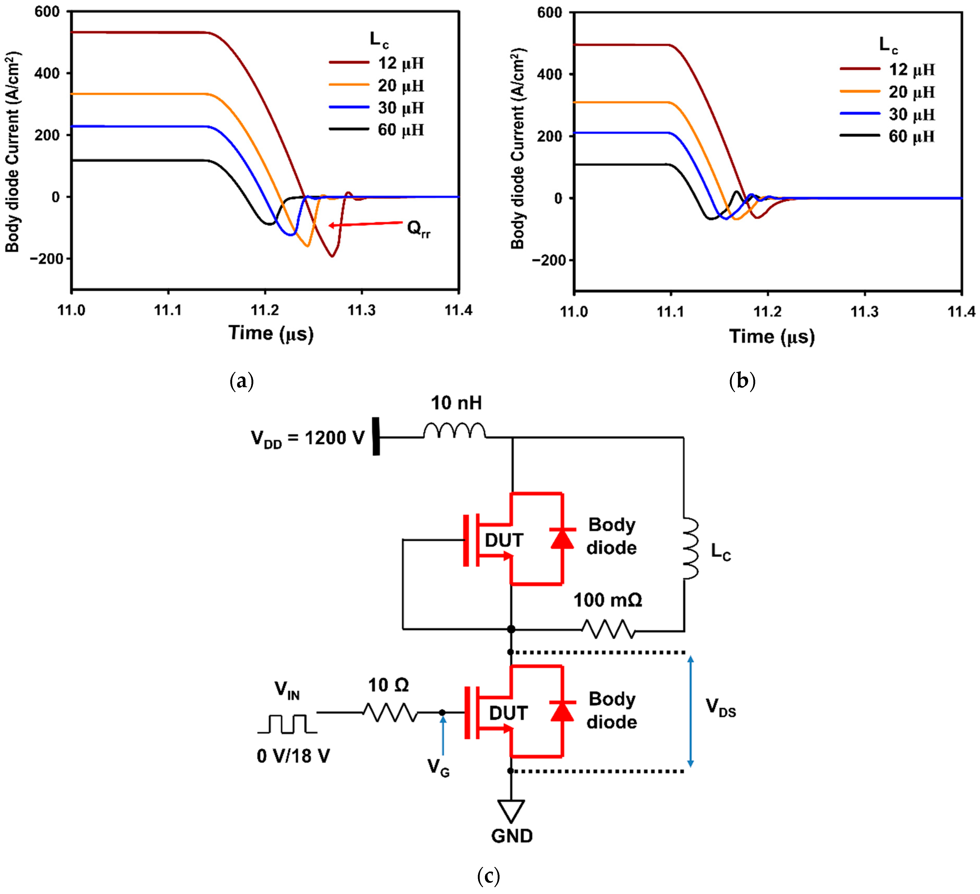
3.2. Body Diode Characteristics

The third quadrant properties of the DT-MOSFET and DTMCD-MOSFET are shown in Figure 9. When the voltage drop between the source and drain of the DT-MOSFET is higher than the knee voltage, the current can flow through the forward PN junction, which is referred to as a PiN body diode [39]. The diode turn-on voltage (VF) is based on the voltage at ISD = 80 A, and the VF of the DT-MOSFET is approximately 2.68 V. However, for a DTMCD-MOSFET, the VF is determined by the threshold voltage on the dummy gate. When the VSD of the dummy gate is above the threshold voltage, a channel forms at the P base of the BPR region, allowing the diode current to flow from the source to the drain, and the channel diode operates. The built-in channel diode in a DTMCD-MOSFET, however, has a lower VF of 1.95 V than that of DT-MOSFET; thus, it is turned on before the PiN diode. Consequently, the operation of the PiN diode of the DTMCD-MOSFET was suppressed, and, since the channel diode had a lower VF, the DTMCD-MOSFET can reduce diode conduction losses compared to the DT-MOSFET.
Figure 10a,b depict the body diode reverse recovery characteristics of the DT-MOSFET and DTMCD-MOSFET according to the LC value, and Figure 10c illustrates a circuit diagram for the double pulsed test (DPT) that was utilized to simulate the switching and reverse recovery characteristics. The reverse recovery charge (Qrr) is defined as:
  Q r r = t 1 t 2   I d ( t )   d t =   Q b i p +   Q o s s
where Qbip is the bipolar stored charge produced when the remaining minority carriers in the drift region are swept out by recombination during the diode turn-off state, Qoss is the capacitance charge produced by the charging displacement current of the output capacitance (Coss), t1 marks the first time that the reverse recovery current drops to zero, and t2 marks the point at which VSD reaches 2% of VDD [40,41,42].
Since the DT-MOSFET uses a PiN body diode as the free-wheeling diode (FWD), both electrons and holes are involved in the current flow. When the diode turns off, due to the requirement for complete recombination of the considerable number of minority carriers still present in the drift region, Qbip is increased [43]. The DTMCD-MOSFET, on the other hand, uses a built-in channel diode as the FWD and has little Qbip since the diode current flow only involves electrons traveling from the drain to the source via the channel. When more diode current flows as the LC value decreases, this difference becomes even more obvious. For DT-MOSFET, Qrr rises as the diode current increases, because more holes remain in the drift region. For the DTMCD-MOSFET, however, there is only a transient caused by Qoss regardless of the amount of the diode current, and the Qrr value is not much of a difference, since there is no hole that influences reverse recovery in this device. The comparison of the reverse recovery characteristics of the DT-MOSFET and MCD-MOSFET is summarized in Table 2.

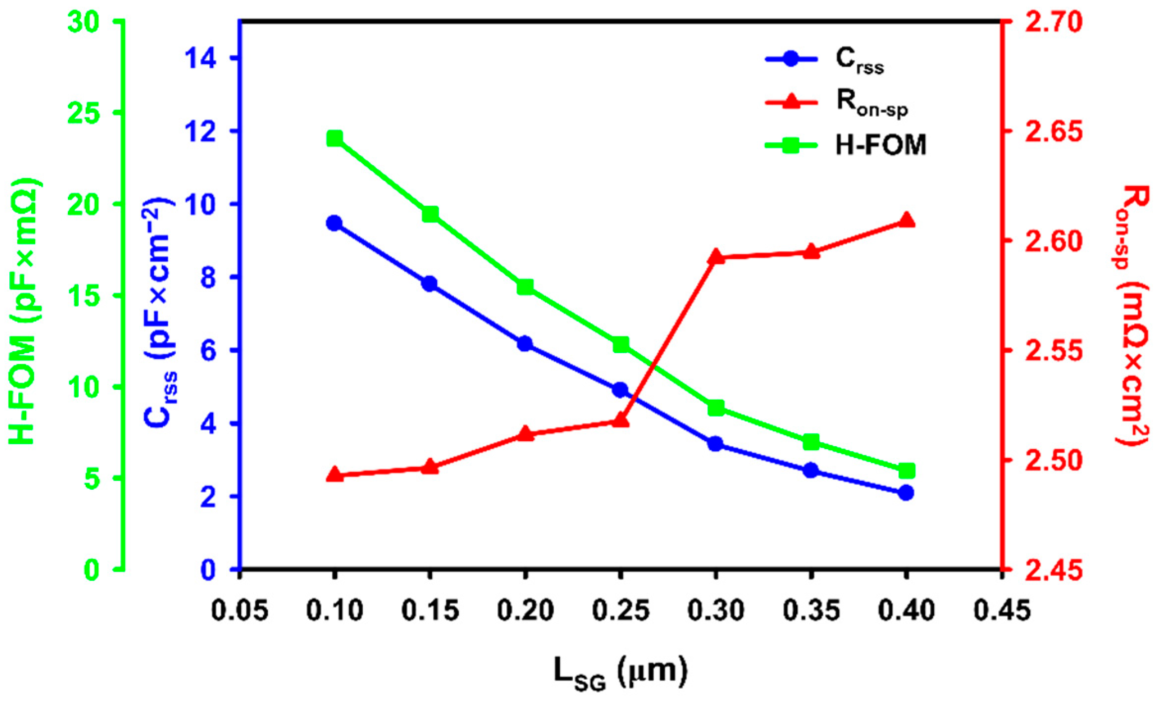
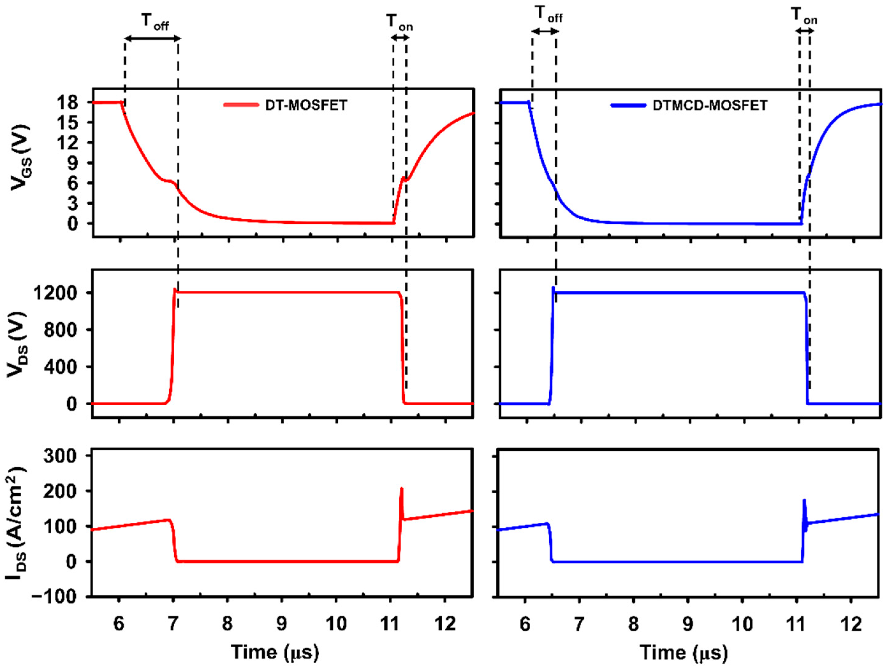
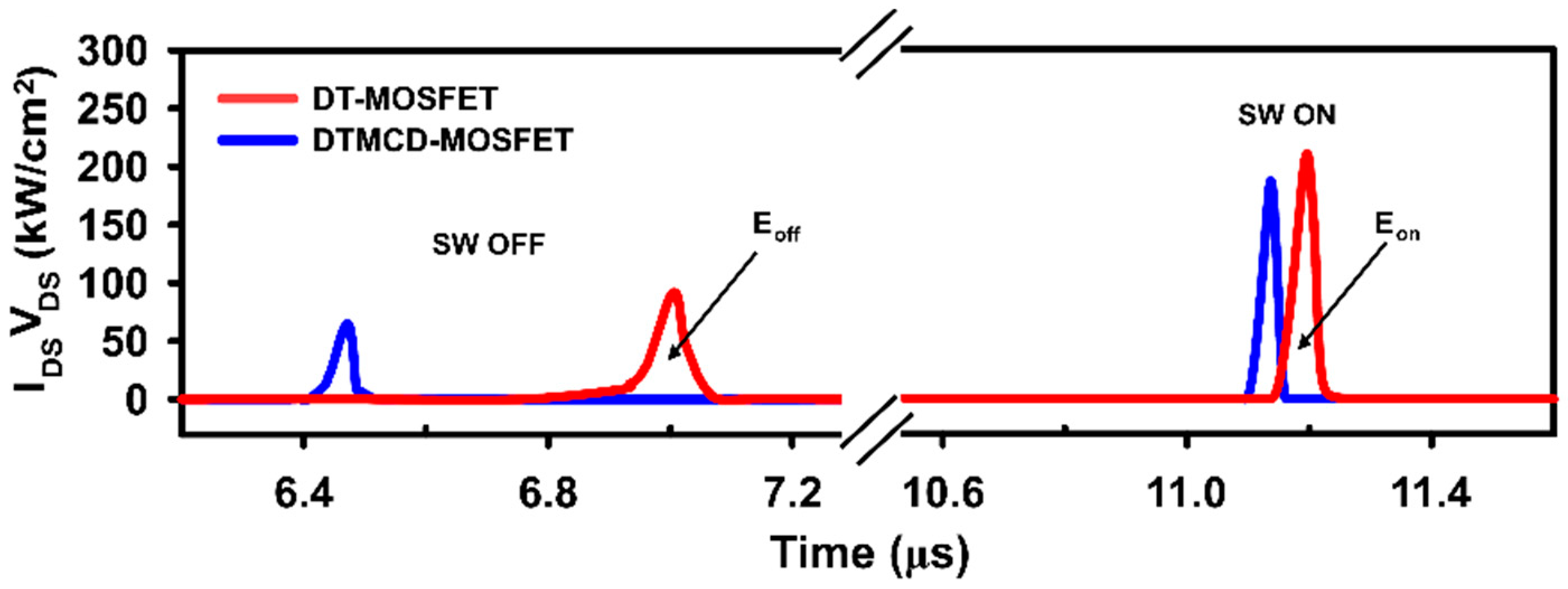
3.3. Dynamic Performances

The characteristics of a DT-MOSFET and a DTMCD-MOSFET’s parasitic capacitance are shown in Figure 11, which includes Ciss (Cgs + Cgd), Crss (Cgd), and Coss (Cds + Cgd) [44]. A gate voltage of 0 V and a small AC signal of 1 MHz were used in the mixed-mode simulation. Since the dummy gate of the DTMCD-MOSFET is connected with the source, the drain-source coupling effect increased, which in turn enhanced Cds. The increased source area does, however, result in a shorter gate length, since there is less overlap between the gate and the drain, which lessens the gate-drain coupling effect. DTMCD-MOSFETs therefore have lower Crss and Ciss than DT-MOSFETs, and Coss also has comparable values as a result of the lower Crss. Because the dummy gate of the DTMCD-MOSFET is in source contact, which caused the CDS to be slightly higher than that of the DT-MOSFET, Coss is almost the same for the two devices as Crss decreases. Compared to the DT-MOSFET, Crss, which affects the switching time, decreased because the overlap area of the gate and drain was reduced. The Crss of the DTMCD-MOSFET was 2.1 pF/cm2, which is a drop of approximately 89.4% from that of the DT MOSFET (19.9 pF/cm2).
Figure 12 depicts the transient response of the gate input voltage, drain voltage, and drain current during the switching on/off operation of the DT-MOSFET and DTMCD-MOSFET. The DPT used for the switching simulation is shown in Figure 8c, and the LC value was set to 60 µH. The switching-on time (Ton) was calculated as the total time required for VGS to reach from 10% of VIN to 90% of VDD (Td-on), and the time required for VDS to reach from 90 to 10% of VDD (Tr) [45]. The switching-off time (Toff) was also calculated as the total time required for VGS to reach from 90% of VIN to 10% of VDD (Td-off), and the time required for VDS to reach from 10 to 90% of VDD (Tf). In the switching behavior of a MOSFET, the gate-source voltage to drain-source voltage switching ratio over time is defined as:
V G S = R G C r s s d V D S d t ( 1 e t R G C i s s )
where the switching time and drain-source voltage change rate are highly dependent on Ciss and Crss components [46]. As the Crss and Ciss values lower, the parasitic capacitance components charge or discharge more quickly in the switching operation, which increases the VDS change rate and decreases the switching time.
The rate of change of VDS in DTMCD-MOSFETs is higher due to their lower Crss and Ciss values compared to the DT-MOSFET, which leads to faster switching times. When compared to the DT-MOSFET, the DTMCD-MOSFET has 55.1% and 31.4% better switching-off and -on times, respectively. The DTMCD-MOSFET exhibited faster switching times than the DT-MOSFET because of its lower Crss.
The switching power dissipations of the DT-MOSFET and the DTMCD-MOSFET are shown in Figure 13. The drain voltage and current in Figure 12 were multiplied to estimate the power dissipation. Calculations for the switching-off loss (Eoff) and switching-on loss (Eon) are as follows:
  E o f f =   T 1   ( 90 %   o f     V G S ) T 1 + T o f f       V D S ( t )   I D S ( t )   d t
  E o f f =   T 2   ( 10 %   o f     V G S ) T 2 + T o n       V D S ( t )   I D S ( t )   d t
where it is estimated by integrating the power dissipation curves over the switching time. DTMCD’s Eoff and Eon can be reduced owing to faster switching times compared to the DT-MOSFET. Furthermore, when the MOSFET is turned on, the load current that was flowing through the free-wheeling body diode and the load inductor during off time transforms into a reverse recovery current and flows to the MOSFET, creating a switching overshoot in the drain current. In comparison to the DT-MOSFET, the DTMCD-MOSFET feature a lower reverse recovery current and charge, which leads to less drain overshoot and thus a lower Eon.
The Eoff and Eon of the DTMCD-MOSFET were reduced by 57.1% and 33.5%, respectively, compared to those of the DT-MOSFET, owing to the fast switching time and low Qrr. Consequently, the total switching loss (Etot; Etot = Eoff + Eon) was reduced by 41.4%. A comparison of the static and dynamic characteristics of the DT-MOSFET and the DTMCD-MOSFET is presented in Table 3.

4. Conclusions

This study proposed a novel 4H-SiC DTMCD-MOSFET with an integrated MOS channel diode. Furthermore, a TCAD simulation is used to examine its static, dynamic, and body diode characteristics. By positioning the channel diode at the bottom of the gate, the proposed MOSFET can activate both side channels of the MOSFET in the on state, thereby minimizing the on-state current decrease caused by single-channel activation in the built-in MCD-MOSFET. Additionally, gate P+ shielding protects the thin gate oxide layer, eliminating any issues with the oxide film dependability caused by strong electric fields. Because the DTMCD-MOSFET has better VF, Qrr, and Crss values than the DT-MOSFET, the Eoff and Eon of the DTMCD-MOSFET were improved by 57.1 and 33.5%, respectively, whereas the Etot was enhanced by 41.4% when compared to the DT-MOSFET. These electrical properties make the DTMCD-MOSFET structure a potential substitute for the conventional devices in high-voltage and high-frequency power circuits.

Author Contributions

Conceptualization, J.N.; methodology, J.N. and K.K.; software, J.N.; validation, J.N. and K.K.; formal analysis, J.N. and K.K.; investigation, J.N.; resources, J.N. and K.K.; writing—original draft preparation, J.N.; writing—review and editing, K.K.; visualization, J.N.; supervision, K.K.; project administration, J.N. and K.K. All authors have read and agreed to the published version of the manuscript.

Funding

This research received no external funding.

Institutional Review Board Statement

Not applicable.

Informed Consent Statement

Not applicable.

Data Availability Statement

Data are not available in a publicly accessible repository and they cannot be shared under request.

Acknowledgments

This paper was supported by a Korea Institute for Advancement of Technology (KIAT) grant funded by the Korean Government (MOTIE) (P0017011, HRD Program for Industrial Innovation), and then by Samsung Electronics.

Conflicts of Interest

The authors declare no conflict of interest.

References

  1. Hamada, K.; Nagao, M.; Ajioka, M.; Kawai, F. SiC―Emerging Power Device Technology for Next-Generation Electrically Powered Environmentally Friendly Vehicles. IEEE Trans. Electron Devices 2015, 62, 278–285. [Google Scholar] [CrossRef]
  2. Baliga, B.J. Silicon Carbide Power Devices; World Scientific: Singapore, 2006; pp. 15–36. [Google Scholar]
  3. Millán, J.; Godignon, P.; Perpiñá, X.; Pérez-Tomás, A.; Rebollo, J. A Survey of Wide Bandgap Power Semiconductor Devices. IEEE Trans. Power Electron. 2014, 29, 2155–2163. [Google Scholar] [CrossRef]
  4. Bharti, D.; Islam, A. Optimization of SiC UMOSFET structure for improvement of breakdown voltage and ON-resistance. IEEE Trans. Electron Devices 2018, 65, 615–621. [Google Scholar] [CrossRef]
  5. Kagawa, Y.; Fujiwara, N.; Sugawara, K.; Tanaka, R.; Fukui, Y.; Yamamoto, Y.; Miura, N.; Imaizumi, M.; Nakata, S.; Yamakawa, S. 4H-SiC Trench MOSFET with Bottom Oxide Protection. Mater. Sci. Forum 2014, 778–780, 919–922. [Google Scholar] [CrossRef]
  6. Nakamura, T.; Nakano, Y.; Aketa, M.; Nakamura, R.; Mitani, S.; Sakairi, H.; Yokotsuji, Y. High performance SiC trench devices with ultra-low Ron. In Proceedings of the 2011 International Device Meeting, Washington, DC, USA, 5–7 December 2011. [Google Scholar]
  7. Zhang, W.; Zhang, L.; Mao, P.; Hou, Y. Characterization of SiC MOSFET switching performance. In Proceedings of the 2018 1st Workshop on Wide Bandgap Power Devices and Applications in Asia (WiPDA Asia), Xi’an, China, 16–18 May 2018. [Google Scholar]
  8. Kyogoku, S.; Tanaka, K.; Ariyoshi, K.; Iijima, R.; Kobayashi, Y.; Harada, S. Role of Trench Bottom Shielding Region on Switching Characteristics of 4H-SiC Double-Trench Mosfets. Mater. Sci. Forum 2018, 924, 748–751. [Google Scholar] [CrossRef]
  9. Morisette, D.T.; Cooper, J.A. Theoretical comparison of SiC PiN and Schottky diodes based on power dissipation considerations. IEEE Trans. Electron Devices 2002, 49, 1657–1664. [Google Scholar] [CrossRef]
  10. Tominaga, T.; Hino, S.; Mitsui, Y.; Nakashima, J.; Kawahara, K.; Tomohisa, S.; Miura, N. Superior Switching Characteristics of SiC-MOSFET Embedding SBD. In Proceedings of the 2019 31st International Symposium on Power Semiconductor Devices and IC’s (ISPSD), Shanghai, China, 19–23 May 2019. [Google Scholar]
  11. Yang, F.; Tian, L.; Shen, Z.; Yan, G.; Liu, X.; Zhao, W.; Wang, L.; Sun, G.; Wu, J.; Zhang, F.; et al. Effects of p-type Islands Configuration on the Electrical Characteristics of the 4H-SiC Trench MOSFETs with Integrated Schottky Barrier Diode. In Proceedings of the 2021 IEEE Workshop on Wide Bandgap Power Devices and Applications in Asia (WiPDA Asia), Wuhan, China, 25–27 August 2021. [Google Scholar]
  12. Tang, L.; Jiang, H.; Wei, J.; Hu, Q.; Zhong, X.; Qi, X. A comparative study of SiC MOSFETs with and without integrated SBD. Microelectron. J. 2022, 128, 105576. [Google Scholar] [CrossRef]
  13. Nicholls, J.; Dimitrijev, S.; Tanner, P.; Han, J. Description and verification of the fundamental current mechanisms in silicon carbide Schottky barrier diodes. Sci Rep. 2019, 9, 3754. [Google Scholar] [CrossRef] [Green Version]
  14. Na, J.; Kim, M.; Kim, K. High Performance 3.3 kV SiC MOSFET Structure with Built-In MOS-Chanel Diode. Energies 2022, 15, 6960. [Google Scholar] [CrossRef]
  15. Deng, X.; Xu, X.; Li, X.; Li, X.; When, Y.; Chen, W. A Novel SiC MOSFET Embedding Low Barrier Diode With Enhanced Third Quadrant and Switching Performance. IEEE Electron Device Lett. 2020, 41, 1472–1475. [Google Scholar] [CrossRef]
  16. Zhou, X.; Gong, H.; Jia, Y.; Hu, D.; Wu, Y.; Xia, T.; Pang, H.; Zhao, Y. SiC Planar MOSFETs With Built-In Reverse MOS-Channel Diode for Enhanced Performance. IEEE J. Electron Devices Soc. 2020, 8, 619–625. [Google Scholar] [CrossRef]
  17. Zhou, X.; Pang, H.; Jia, Y.; Hu, D.; Wu, Y.; Tang, Y.; Xia, T.; Gong, H.; Zhao, Y. SiC Double-Trench MOSFETs with Embedded MOS-Channel Diode. IEEE Trans. Electron Devices 2020, 67, 582–587. [Google Scholar] [CrossRef]
  18. Vudumula, P.; Kotamraju, S. Design and Optimization of 1.2-kV SiC Planar Inversion MOSFET Using split Dummy Gate Concept for High-Frequency Applications. IEEE Trans. Electron Devices 2019, 66, 5266–5271. [Google Scholar] [CrossRef]
  19. Yu, H.; Liang, S.; Liu, H.; Wang, J.; Shen, Z.J. Numerical Study of SiC MOSFET With Integrated n-/n-Type Poly-Si/SiC Heterojunction Freewheeling Diode. IEEE Trans. Electron Devices 2021, 68, 4571–4576. [Google Scholar] [CrossRef]
  20. Singh, R.; Hefner, A.R. Reliability of SiC MOS devices. Solid State Electron. 2004, 48, 1717–1720. [Google Scholar] [CrossRef]
  21. Liu, T.; Zhu, S.; White, M.H.; Salemi, A.; Sheridan, D.; Agarwal, A.K. Time-dependent dielectric breakdown of commercial 1.2 kV 4H-SiC power MOSFETs. IEEE J. Electron Devices Soc. 2021, 9, 633–639. [Google Scholar] [CrossRef]
  22. Na, J.; Cheon, J.; Kim, K. High performance 4H-SiC MOSFET with deep source trench. Semicond. Sci. Technol. 2022, 37, 045004. [Google Scholar] [CrossRef]
  23. Han, K.; Baliga, B.J.; Sung, W. Split-Gate 1.2-kV 4H-SiC MOSFET: Analysis and Experimental Validation. IEEE Electron Device Lett. 2017, 38, 1437–1440. [Google Scholar] [CrossRef]
  24. Han, K.; Baliga, B.J.; Sung, W. A Novel 1.2 kV 4H-SiC Buffered-Gate (BG) MOSFET: Analysis and Experimental Results. IEEE Electron Device Lett. 2018, 39, 248–251. [Google Scholar] [CrossRef]
  25. Tyagi, R.; Ghezzo, M.; Chow, T.P.; Norton, J.F. An Isoplanar Isolation Technology for SiC Devices Using Local Oxidation. J. Electrochem. Soc. 1994, 141, 2188. [Google Scholar] [CrossRef]
  26. Mehregany, M.; Zorman, C.A. SiC MEMS: Opportunities and challenges for applications in harsh environments. Thin Solid Film. 1999, 355–356, 518–524. [Google Scholar] [CrossRef]
  27. Melloch, M.R.; Cooper, J.A. Fundamentals of SiC-based device processing. MRS Bull. 1997, 22, 42–47. [Google Scholar] [CrossRef]
  28. Yazdanfar, M.; Ivanov, I.G.; Pedersen, H.; Kordina, O.; Janzén, E. Reduction of structural defects in thick 4H-SiC epitaxial layers grown on 4° off-axis substrates. J. Appl. Phys. 2013, 113, 223502. [Google Scholar] [CrossRef] [Green Version]
  29. Agarwal, A.; Baliga, B.J.; Francois, M.M.A.; Maxwell, E.; Berliner, N.; Papageorge, M. 3.3 kV 4H-SiC Planar-Gate MOSFETs Manufactured using Gen-5 PRESCIETM Technology in a 4-inch Wafer Commercial Foundry. In Proceedings of the SoutheastCon 2021, Atlanta, GA, USA, 10–14 March 2021. [Google Scholar]
  30. Shen, H.-J.; Tang, Y.-C.; Peng, Z.-Y.; Deng, X.-C.; Bai, Y.; Wang, Y.-Y.; Li, C.-Z.; Liu, K.-A.; Liu, X.-Y. Fabrication and Characterization of 1700 V 4H-SiC Vertical Double-Implanted Metal-Oxide-Semiconductor Field-Effect Transistors. Chin. Phys. 2015, 32, 127101. [Google Scholar] [CrossRef]
  31. Kobayashi, Y.; Harada, S.; Ishimori, H.; Takasu, S.; Kojima, T.; Ariyoshi, K.; Sometani, M.; Senzaki, J.; Takei, M.; Tanaka, Y.; et al. 3.3kV-Class 4H-SiC UMOSFET by Double Trench with Tilt Angle Ion Implantation. Mater. Sci. Forum 2016, 858, 974–977. [Google Scholar] [CrossRef]
  32. Horiike, Y.; Ichihara, T.; Sakaue, H. Filling of Si oxide into a deep trench using digital CVD method. App. Surf. Sci. 1990, 46, 168–174. [Google Scholar] [CrossRef]
  33. Lu, J.; Liu, H.; Luo, J.; Wang, L.; Li, B.; Li, B.; Zhang, G.; Han, Z. Improved single-event hardness of trench power MOSFET with a widened split gate. In Proceedings of the 2016 16th European Conference on Radiation and Its Effects on Components and Systems (RADECS), Bremen, Germany, 19–23 September 2016. [Google Scholar]
  34. Goarin, P.; Koops, G.E.J.; Van Dalen, R.; Cam, C.L.; Saby, J. Split-gate resurf Oxide (RSO) MOSFETs for 25V applications with low gate-to-drain charge. In Proceedings of the 19th International Symposium on Power Semiconductor Devices & ICs, Jeju, Korea, 27–30 May 2007. [Google Scholar]
  35. Park, C.; Havanur, S.; Shibib, A.; Terrill, K. 60 V rating split gate trench MOSFETs having best-in-class specific resistance and figure-of-merit. In Proceedings of the 28th International Symposium on Power Semiconductor Devices & ICs, Prague, Czech Republic, 12–16 June 2016. [Google Scholar]
  36. Takaya, H.; Morimoto, J.; Hamada, K.; Yamamoto, T.; Sakakibara, J.; Watanabe, Y.; Soejima, N. A 4H-SiC trench MOSFET with thick bottom oxide for improving characteristics. In Proceedings of the 25th International Symposium on Power Semiconductor Devices & ICs (ISPSD), Kanazawa, Japan, 26–30 May 2013. [Google Scholar]
  37. Synopsys, Inc. TCAD SentaurusTM Device User Guide; Synopsys INC.: Mountain View, CA, USA, 2017. [Google Scholar]
  38. Agarwal, A.K.; Siergiej, R.R.; Seshadri, S.; White, M.H.; McMullin, P.G.; Burk, A.A.; Rowland, L.B.; Brandt, C.D.; Hopkins, R.H. A critical look at the performance advantages and limitations of 4H-SiC power UMOSFET structures. In Proceedings of the 8th International Symposium on Power Semiconductor Devices & ICs (ISPSD), Maui, HI, USA, 23 May 1996. [Google Scholar]
  39. Kimoto, T.; Yamada, K.; Niwa, H.; Suda, J. Promise and Challenges of High-Voltage SiC Bipolar Power Devices. Energies 2016, 9, 908. [Google Scholar] [CrossRef] [Green Version]
  40. Sochor, P.; Huemer, A.; Hell, M.; Elpelt, R. Understanding the Turn-off Behavior of SiC MOSFET Body Diodes in Fast Switching Applications. In Proceedings of the PCIM Europe Digital Days 2021, International Exhibition and Conference for Power Electronics, Intelligent Motion, Renewable Energy and Energy Management, Online, 3–7 May 2021. [Google Scholar]
  41. Dalal, D.N.; Christensen, N.; Jorgensen, A.B.; Jorgensen, J.K.; Beczkowski, S.; Munknielsen, S.; Uhrenfeldt, C. Impact of power module parasitic capacitances on medium voltage sic mosfets switching transients. IEEE J. Emerg. Sel. Top. Power Electron 2019, 8, 298–310. [Google Scholar] [CrossRef]
  42. Yan, Q.; Yuan, X.; Geng, Y.; Charalambous, A.; Wu, X. Performance Evaluation of Split Output Converters with SiC MOSFETs and SiC Schottky Diodes. IEEE Trans. Power Electron 2017, 32, 406–422. [Google Scholar] [CrossRef] [Green Version]
  43. Wei, W.; Li, J.; Zhao, S. Numerical analysis of reverse recovery characteristics of 4H-SiC p+–n–n+ power diode with injection conditions. App. Phys. A 2015, 118, 1387–1398. [Google Scholar] [CrossRef]
  44. Han, K.; Baliga, B.J. Comparison of Four Cell Topologies for 1.2-kV Accumulation- and Inversion- Channel 4H-SiC MOSFETs: Analysis and Experimental Results. IEEE Trans. Electron Devices 2019, 66, 2321–2326. [Google Scholar] [CrossRef]
  45. Cheon, J.; Kim, K. Numerical Simulation Analysis of Switching Characteristics in the Source-Trench MOSFET’s. Electronics 2020, 9, 1895. [Google Scholar] [CrossRef]
  46. Yuan, D.; Zhang, Y.; Wang, X. An Improved Analytical Model for Crosstalk of SiC MOSFET in a Bridge-Arm Configuration. Energies 2021, 14, 683. [Google Scholar] [CrossRef]
Figure 1. Cross-sectional view of (a) DT-MOSFET and (b) DTMCD-MOSFET.
Electronics 12 00092 g001
Figure 2. Comparisons of the specific on-resistance (Ron-sp), gate-drain capacitance (Crss), and H-FOM characteristics for different LSG of DTMCD-MOSFET.
Electronics 12 00092 g002
Figure 3. Proposed fabrication procedure of DTMCD-MOSFET. (a) N-drift region and CSL region formed by epitaxial growth on N+ substrate. (b) BPR region formed by ion implantation. (c) Left CSL region and P-base region formed by epitaxial growth; implant N+ source region. (d) Trench the source region using RIE etching, and implant P+ region using tilt-ion implantation. (e) Fill the source trench with oxide through CVD. (f) The gate region trenched; perform the wet thermal oxidation. (g) The N+ Polysilicon deposited and etched, forming a dummy gate. (h) Wet thermal oxidation conducted again. (i) Form an active gate through the deposit of the N+ Polysilicon and the etch-back process. After that, ILD oxide is deposited through the CVD. (j) Etch the oxide and complete metallization.
Electronics 12 00092 g003
Figure 4. Comparison of the on-state characteristics of DT-MOSFET and proposed DTMCD-MOSFET.
Electronics 12 00092 g004
Figure 5. Cross-sectional view of electron current density distribution of (a) proposed DTMCD-MOSFET with horizontally separated gate structure and (b) DTMCD-MOSFET with vertically separated gate structure.
Electronics 12 00092 g005
Figure 6. Comparison of the on-state characteristics of two MOSFETs with gate structures separated in horizontal and vertical directions, respectively.
Electronics 12 00092 g006
Figure 7. Comparison of off-state characteristics of DT-MOSFET and DTMCD-MOSFET.
Electronics 12 00092 g007
Figure 8. Cross-sectional view of the electric field distribution of (a) DT-MOSFET and (b) DTMCD-MOSFET at VDS = 1200 V.
Electronics 12 00092 g008
Figure 9. Third quadrant characteristics of DT-MOSFET and DTMCD-MOSFET.
Electronics 12 00092 g009
Figure 10. Comparison of the reverse recovery characteristics with different LC of (a) DT-MOSFET (b) DTMCD-MOSFET (c) Circuit diagram of double pulsed test for switching.
Electronics 12 00092 g010
Figure 11. Parasitic gate-drain capacitance, input and output capacitance curves of DT-MOSFET and DTMCD-MOSFET with VGS = 0 V.
Electronics 12 00092 g011
Figure 12. Switching waveforms of DT-MOSFET and DTMCD-MOSFET.
Electronics 12 00092 g012
Figure 13. Comparison of the power dissipations of DT-MOSFET and DTMCD-MOSFET during the switching transient.
Electronics 12 00092 g013
Table 1. Device parameters comparison.
ParameterDT–DTMCD–
Cell pitch [μm]4.84.8
Gate trench width [μm]1.21.2
Source trench width [μm]0.60.6
Source trench depth [μm]1.51.5
N-drift thickness [μm]1010
Tox1 [nm]5050
Tox2 [nm]-210
Tox3 [nm]-10
BPR width [μm]1.11.1
BPR depth [μm]55
LSG [μm]-0.4
N-drift doping concentration [cm−3]7 × 10157 × 1015
CSL doping concentration [cm−3]2 × 10162 × 1016
P+ doping concentration [cm−3]2 × 10182 × 1018
P-base doping concentration [cm−3]2 × 10172 × 1017
N+ doping concentration [cm−3]1 × 10191 × 1019
Table 2. Reverse recovery charge according to LC value.
ParameterDT–DTMCD–
Qrr (@LC = 60 µH) [µC·cm−2]2.331.62
Qrr (@LC = 30 µH) [µC·cm−2]3.171.47
Qrr (@LC = 20 µH) [µC·cm−2]3.791.51
Qrr (@LC = 12 µH) [µC·cm−2]4.781.4
Table 3. Static and dynamic characteristics of devices.
ParameterDT–DTMCD–
BV [V]21372139
Ron-sp [mΩ·cm2]2.482.61
EMOX (@VDS = 1.2 kV) [MV/cm]1.411.14
VF (@ISD = 80 A·cm−2) [V]2.681.95
Ciss (@VDS = 1.2 kV) [nF·cm−2]36.321.1
Coss (@VDS = 1.2 kV) [pF·cm−2]839839
Crss (@VDS = 1.2 kV) [pF·cm−2]19.92.1
H–FOM [pF·mΩ]49.45.5
Ton [ns]159109
Toff [ns]917412
Eon [mJ·cm−2]8.0455.352
Eoff [mJ·cm−2]4.0871.753
Etot [mJ·cm−2]12.1327.105
Disclaimer/Publisher’s Note: The statements, opinions and data contained in all publications are solely those of the individual author(s) and contributor(s) and not of MDPI and/or the editor(s). MDPI and/or the editor(s) disclaim responsibility for any injury to people or property resulting from any ideas, methods, instructions or products referred to in the content.

