Communication

Thermal Performance of Cu Electroplated GaN/AlGaN High-Electron-Mobility Transistors with Various-Thickness Si Substrates

1
Institute of Electronics, National Yang Ming Chiao Tung University, Hsinchu 30010, Taiwan
2
International College of Semiconductor Technology, National Yang Ming Chiao Tung University, Hsinchu 30010, Taiwan
*
Author to whom correspondence should be addressed.
Electronics 2023, 12(9), 2033; https://doi.org/10.3390/electronics12092033
Submission received: 10 April 2023 / Revised: 25 April 2023 / Accepted: 26 April 2023 / Published: 27 April 2023
(This article belongs to the Special Issue Wide Bandgap Semiconductor: From Epilayer to Devices)

Abstract

:
Thermal dissipation is an important issue for power devices. In this work, the impact of thermal effects on the performance of Cu electroplated GaN-based high-electron-mobility transistors (HEMTs) are considered. Electrical, thermometry and micro-Raman characterization techniques were used to correlate the effects of improved heat dissipation on device performance for GaN HEMTs with different thicknesses of Si substrate (50, 100, 150 μm), with and without an additional electroplated Cu layer. GaN HEMTs on electroplated Cu on Si (≤50 μm) demonstrate an enhanced on/off current ratio compared to bare Si substrate by a factor of ~400 (from 9.61 × 10⁵ to 4.03 × 10⁸). Of particular importance, surface temperature measurements reveal a much lower channel temperature for thinner HEMT devices with electroplated Cu samples compared to those without.

1. Introduction

Gallium nitride (GaN) is a wide-bandgap semiconductor material and is currently being explored for state-of-the-art high-power, high-frequency and optoelectronic device applications. This is due in part to its large electric breakdown field and the presence of a bandgap discontinuity between GaN and AlGaN. Moreover, the existing polarization field creates a large two-dimensional (2-D) electron gas concentration [1,2,3,4]. Following reports of AlGaN/GaN heterostructure-based transistors on Si substrate, which hold greater potential for scale-up at lower cost, rapid growth in GaN-based devices has been reported [5]. Moreover, GaN-based HEMTs with greater efficiency, higher power handling capacity and higher density are under exploration to meet the demands of next-generation computers and connecting networks [6]. GaN-based HEMTs also show potential for high-power sub-millimeter wave RF and microwave applications in satellite communications including 5G/6G technologies [7]. AlGaN/GaN heterostructure-based high-electron-mobility transistors (HEMTs) have been widely studied for high-power and high-frequency applications due to their high electron density, high thermal stability, high drift velocity and large electric breakdown field [8,9,10,11,12,13,14]. Furthermore, other high-power systems, such as high-concentration III–V multijunction solar cells, also require efficient heat dissipation solutions [15,16,17].
Unfortunately, AlGaN/GaN-based devices possess self-heating effects degrading drain current saturation as well as transconductance, lowering overall device performance. Reports suggest self-heating and elevated channel temperatures are linked to the transfer of energy from electron to lattice [18,19,20]. Consequently, a reduction in electron mobility and saturation velocity is expected as a result of phonon scattering [21,22]. Various methods have been reported to aid heat dissipation by employing highly thermally conductive materials such as SiC and diamond. The presence of metallic impurities such as Al and N in the case of SiC and N impurity in the case of diamond yields a rapid decrease in thermal conductivity at higher temperatures linked to phonon scattering [23]. Another key problem is that these substrates are not currently cost-effective and scalable; moreover, in the case of diamond, direct deposition on GaN remains challenging. Alternatively, composite substrates and flip chip bonding techniques with an epoxy under-fill have been employed to reduce thermal impedance for entire wafers [24,25]. However, the existence of hot spots in the channel region remains. In previous studies, a reduction in self-heating via substrate transfer was reported [26,27], and heat dissipation by employing diamond nanostructures on the device surface with moderate improvements was reported [28,29].
In most studies, local removal of the Si substrate to improve heat dissipation has been the usual approach, but self-heating effects persist. Similar behavior has been reported by P. Srivastva et al. [30,31]. Pvlidis et al. reported thermal measurements of HEMTs; here, AlN was deposited on the backside of trench-etched AlGaN layers followed by Cu (2 µm) deposition. In this case, inferior thermal performance was reported compared to Si substrate-based devices without trenches [32]. This may be associated with increased thermal resistance as a result of AlN deposition after Si removal. Further, highly thermally conductive metals such as Cu were employed to fill trench structures on Si to enhance heat dissipation and improve device performance [33,34]. Hsueh et al. reported an AlGaN/GaN metal–insulator–semiconductor HEMT using a through-substrate via and backside metal with low leakage current for Vgs in the 0 to −10 V range [35]. However, trench filling with Cu was not discussed. A simulation study by Hwang et al. suggested a new approach to improve heat dissipation and reduce junction temperature of AlGaN/GaN HEMTs using a Cu-filled via-hole under the active area of the device on Si substrate [36]. Simulations by Jang et al. consider the performance optimization of AlGaN/GaN HEMT devices through Cu-filled trench structures [37]. Recently, in another study [38,39,40,41,42], a GaN/Si HEMT with improvements in drain current saturation and transconductance with a stable threshold voltage using Cu-filled trenches (Si substrate) or nanocrystalline diamond capping layers was reported. Although thin epilayers of AlGaN/GaN HEMTs on Cu have been reported [43,44], the transfer of a 3 μm thick GaN layer grown on silicon can yield high-stress gradients arising from a large lattice and thermal mismatch and thus eventual cracking. One potential solution to improve fabrication yield is to leave a partial Si layer on the epilayer itself. However, the effect of Si substrate thickness with an electroplated Cu layer on HEMT performance was not studied.
This work discusses the utilization of an AlGaN/GaN HEMT device with an electroplated thick Cu layer instead of a locally removed Si substrate. Table 1 shows the thermal conductivity and thermal expansion coefficients of Si and Cu. However, the influence of the remaining Si substrate thickness or complete substrate removal on device characteristics was not studied. In this study, the GaN/AlGaN HEMT devices with different Si substrate thicknesses before and after Cu electroplating were investigated.

2. Experimental Details

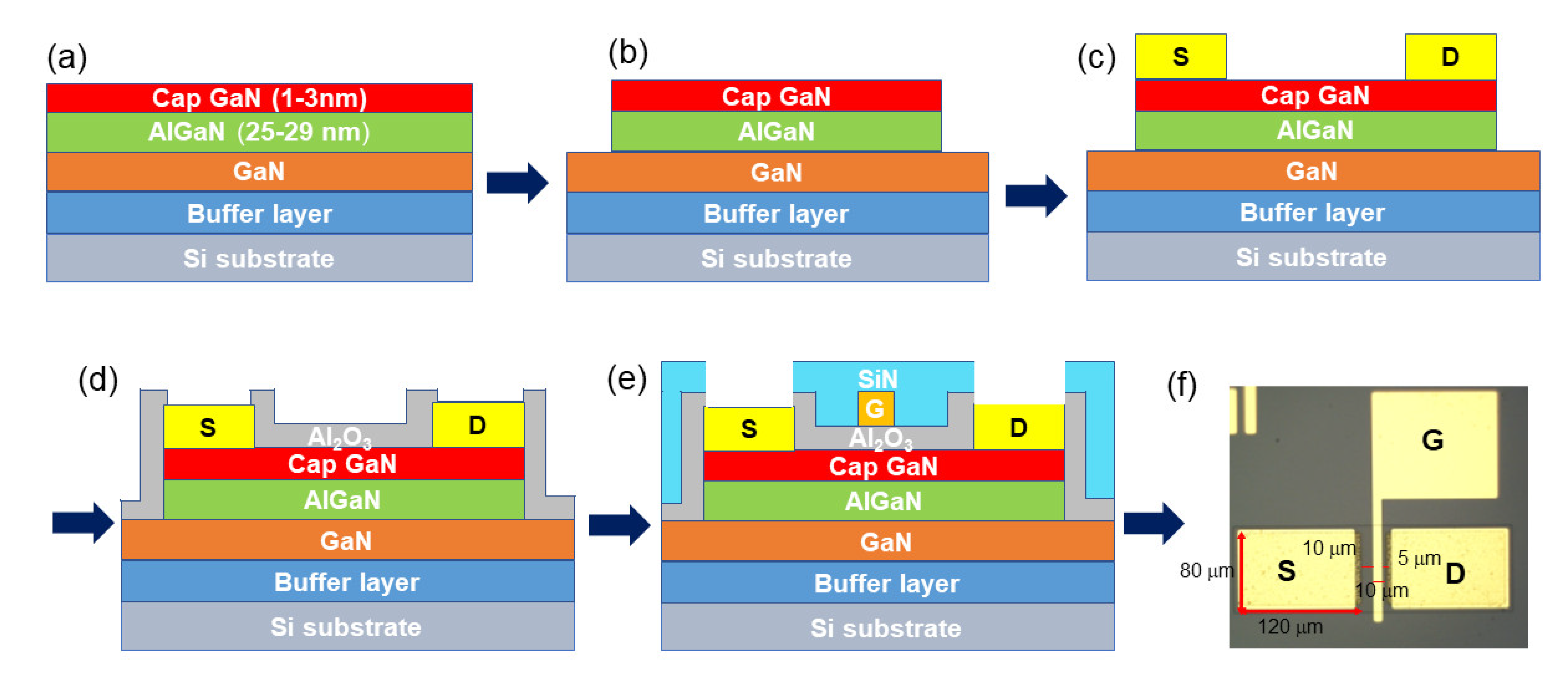
2.1. HEMT Device Fabrication

GaN/AlGaN HEMT epilayers were grown on 6-inch Si (111) substrate by metal organic chemical vapor deposition (MOCVD). The device structure consists of GaN (1–3 nm), AlGaN (25–28 nm) and a buffer layer with a combined thickness of 5.5 µm, shown in Figure 1a. After epitaxial growth, the mobility, channel density and sheet resistivity were 1550 cm2/V.s, 9 × 10¹²/cm2 and 550 Ω/□ obtained by Hall effect measurement. This first step was performed by mesa etching using an inductively coupled plasma reactive ion etching (ICP-RIE) system, as shown in Figure 1b. The etching parameters were ICP power 350 W and RF power 40 W using Ar, Cl and SiCl4 with flow rates of 25 sccm, 8 sccm and 7 sccm, respectively. The source (S) and drain (D) electrodes were fabricated by depositing a Ti/Al/Ni/Au metal stack of 30/180/40/100 nm thickness using E-beam evaporation, as shown in Figure 1c. Thereafter, rapid thermal annealing (RTA) was performed at 850 °C for 60 s in a nitrogen atmosphere to obtain Ohmic characteristics for the source/GaN cap layer/drain. In subsequent steps shown in Figure 1d, a 20 nm thin Al2O3 gate oxide layer was deposited by atomic layer deposition at 250 °C using trimethylaluminum and H2O. A pattern was then developed to open the source and drain contact. Then, ICP-RIE was used for Al2O3 etching. For the gate electrode, a Ni/Au stack of 25/1150 nm thickness was deposited by an E-beam evaporation system. SiNx was then deposited as a passivation layer, and a contact pad pattern was developed. ICP-RIE was used to etch SiNx for S, D and G metal contacts, shown in Figure 1e. Finally, the contact metals for S, D and G were deposited; an optical microscope image of the fabricated HEMT device is shown in Figure 1f. The optimized Ohmic contact parameters have been studied in detail by machine learning [45].

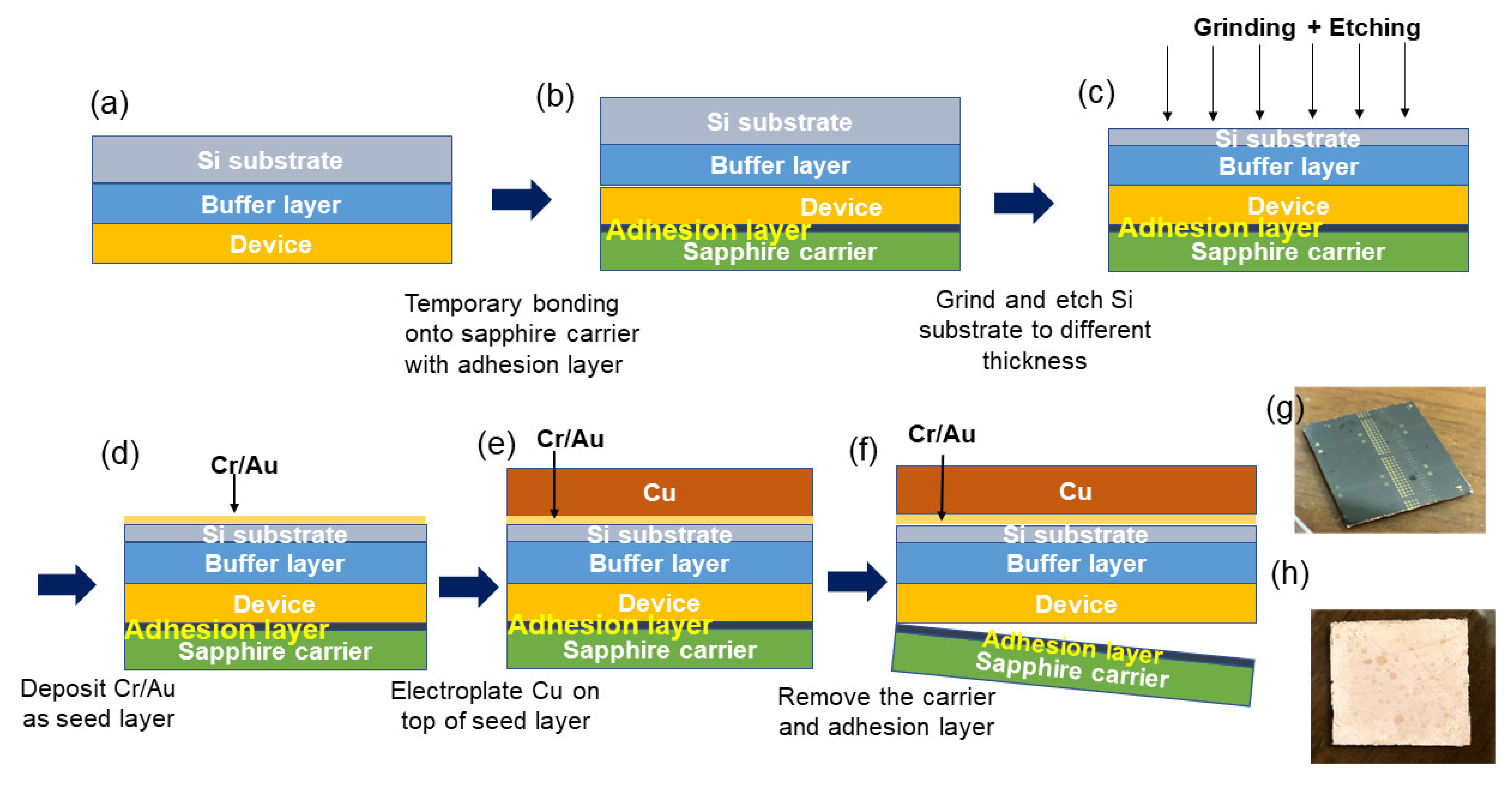
2.2. Electroplating of Cu on Backside of HEMT Device

The complete backside process is shown in Figure 2. The fabricated device on the Si substrate was first bonded to sapphire using a template adhesive layer from the device side, as shown in Figure 2b. Then, the Si substrate was reduced to 150 µm by grinding to reduce the etching time. To obtain precise control of Si thickness, thinning of the Si substrate was realized by wet chemical treatment, as shown in Figure 2c. The chemical etchant contained hydrochloric acid (HCl), nitric acid (HNO3) and acetic acid (CH3COOH). Four different samples of Si substrate thickness of 150, 100, 50 µm and 0 µm (Si completely removed) were prepared at an etching rate of 5 µm/min. The thicknesses of Si substrates were confirmed by cross-sectional measurements using an optical microscope. As the Si substrate was completely removed, the sample color changed from grey to transparent. Prior to Cu electroplating, a seed layer of Cr/Au of 60/100 nm thickness was deposited by thermal evaporation, as shown in Figure 2d. The Cu permanent substrate with 50 µm thickness was deposited by electroplating at a rate of 15μm/h as shown in Figure 2e. After electroplating, samples were immersed in an anti-fogging solution for 15 s to prevent copper oxidization. The carrier substrate (sapphire) was then removed, and the samples were immersed in acetone to dissolve the adhesive layer, as shown in Figure 2f. Finally, the samples were cleaned, rinsed and dried using a standard process to remove chemical residue. Note that there was no damage observed from the adhesion layer between the device and the sapphire substrate. Figure 2g,h show optical microscope images of the front and back sides of the HEMT device after Cu electroplating, respectively.
After processing, electrical characterization was performed using an Agilent B1505A power device analyzer at room temperature. The transmission length method was utilized to extract parameters related to material resistance and Ohmic contacts. Infrared thermal imaging was used to measure the device’s surface temperature. The stress of GaN HEMTs with different thicknesses before and after electroplating was measured by Raman spectroscopy (LABRAM HR 800 UV, Horiba/Jobin-Yvon, Longjumeau, France) at room temperature. The excitation wavelength was 488 nm (argon laser). In order to avoid the effect of epilayer quality, samples were prepared using the same epi-wafer for comparison before and after backside processing.

3. Results

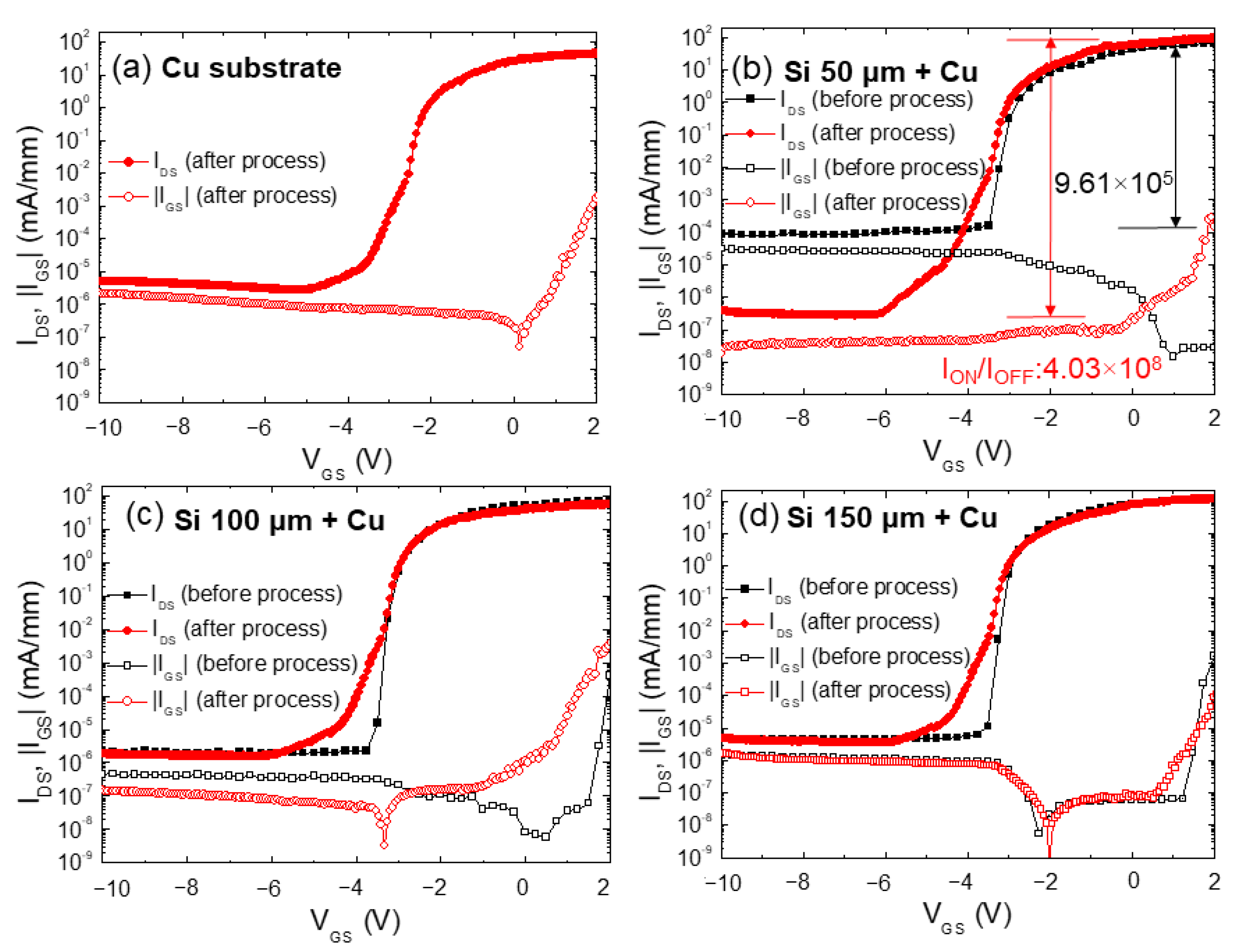
3.1. Electrical Characteristics of HEMT Devices with and without Electroplated Cu

The detailed DC characteristics of fabricated GaN/AlGaN HEMT devices before and after the backside process were studied by measuring IDS and |IGS| as a function of VGS. Here, the IDS and |IGS| were normalized for a gate width of 80 μm, and device dimensions are shown in Figure 1f. Figure 3a,b illustrate the IDS-VGS measurements at VDS = 4 for samples with only a 50 µm thick Cu substrate and for those on 50 µm thick Si substrate before and after the backside process (BSP), i.e., in comparison with electroplated Cu layers. For samples where the Si substrate was completely etched away, leakage current dropped to ~ 10−5 mA/mm, as shown in Figure 3a. The authors note that HEMT transfer characteristics shown in Figure 3a prior to the backside process cannot be measured owing to the remaining GaN HEMT epilayer being <6 µm (it was too thin to measure). A two-order drop in leakage current from 10−4 mA/mm to <10−6 mA/mm and an increment in the switching ratio from 9.61 × 10⁵ to 4.03 × 10⁸ can be observed in Figure 3b for samples with a 50 µm thick Si substrate before and after Cu plating, respectively. Here, IDS values are affected not only by self-heating, but also by HEMT epilayer stress. The epilayers were designed to have compressive stress during growth and are counterbalanced by Si substrate stress during post-growth cooldown. As the Si substrate is removed, the GaN HEMT epilayer can return to a compressive stress state. Although the epilayer was electroplated with Cu, the tensile stress of the GaN epilayer should be smaller than that of GaN on a Si substrate with a Cu film. Consequently, the IDS (shown in Figure 3a) of the GaN HEMT solely with Cu metal was smaller than that (shown in Figure 3b,c) of a GaN HEMT with combined Si and Cu metal substrates. For samples with 100 µm and 150 µm of Si substrate before and after Cu plating, leakage current did not decrease significantly; moreover, current switching was maintained at around 107, as shown in Figure 3c,d. In terms of |IGS|, these values ranged from 10−6 to 10−8 mA/mm as VGS was less than 0 V for all samples. Even for a positive applied VGS, measured values were <10−3 mA/mm for all samples.
For comparison, the IDS−VGS measurements for all four samples with electroplated Cu on different Si substrate thicknesses are shown in Figure 4. The lowest leakage current was observed for Cu electroplated on a 50 µm Si substrate. Furthermore, the device threshold voltage (Vth) after removal of the Si substrate was on the right side compared to devices with different Si substrate thicknesses on Cu substrates. For devices on 650 µm thick Si substrate (before BSP), Vth was approximately −3 V. After thinning and electroplating with Cu, Vth was −8, −7 and −6 V for HEMTs with Si thicknesses of 150 µm, 100 µm and 50 µm, respectively. Moreover, Vth recovered to −5 V for the HEMT with only a Cu substrate. Threshold voltage increased from −8 V to −6 V with Si substrate thinning and recovered to −5 V after Si substrate removal. This may be attributable to residual stress variations and will be discussed in the Raman measurement section.
Figure 5 shows the ID-VDS characteristics of fabricated devices with different Si substrate thicknesses before and after BSP where VGS varies from −5 V to 1 V in intervals of 1 V. After substrate etching and Cu electroplating, all samples with different Si thicknesses and Cu substrates demonstrate an increasing trend in drain current as compared with those without electroplated Cu. As in HEMT devices, current amplitude is impacted by temperature variation. In this case, as channel temperature rises upon increasing voltage, electron mobility reduces and thus current levels decrease. However, owing to enhanced heat dissipation, drain current density is increased compared to devices without said process. A fairly significant difference in current can be seen in Figure 5. At VGS = 1 V and VDS = 9 V, an increased current from 100 mA/mm to 130 mA/mm is recorded for a 50 µm Si and Cu substrate, shown in Figure 5b, representing a 30% increase in measured drain current. For the corresponding HEMT, the Ron value before and after Cu electroplating was 685 Ω and 687 Ω, respectively. Likewise, for the HEMT on 100 µm thick Si with and without Cu, a current increase to 140 mA/mm from 120 mA/mm is seen, shown in Figure 5c, representing a 17% increase in measured drain current. The corresponding HEMT Ron for a 100 µm thick Si before and after Cu electroplating was 572 Ω and 570 Ω, respectively. Furthermore, a current increase to 140 mA/mm from 130 mA/mm, shown in Figure 5d, represents a 7% increase in measured drain current for the HEMT sample on 150 µm thick Si. The corresponding Ron of a HEMT with 150 µm thick Si before and after Cu electroplating was 535 Ω and 548 Ω, respectively. This approach suggests Cu electroplating can improve heat dissipation and enhance device current capability. Nevertheless, it was found that Ron of HEMTs with different Si substrate thicknesses after Cu electroplating can increase somewhat. It was observed that thinner Si substrates can lead to higher Ron HEMT values, which could be attributable to stress variations impacting 2DEG density. This point will be discussed later.
Clearly, thinner Si substrates can permit greater heat (resulting from device self-heating) transfer to the more thermally conductive Cu substrate, assuming negligible thermal boundary resistance. It is this scenario that is believed to contribute to IDS increasing after substrate thinning and Cu electroplating. It is also worth stating that individual IDS HEMT values were different prior to electroplating due to differing Si substrate thicknesses impacting device self-heating and eventual heat transfer. Concerning the IDS values, one must consider self-heating effects and HEMT epilayer stress. As is well known, the epilayers were designed to have compressive stress during growth, later to be balanced by Si substrate stress during post-growth temperature cooldown. As the Si substrate was totally removed, the GaN HEMT epilayer could return to a compressive stress condition. Although Cu was electroplated on the epilayer, the tensile stress of the GaN epilayer is likely smaller than that of GaN with a combined Si and Cu plated substrate. As a consequence, the IDS (shown in Figure 5a) of a GaN HEMT/Cu was smaller than that (shown in Figure 5b,c) of a GaN HEMT/ Si/Cu configuration. The obtained result is consistent with the observed Ron behavior.

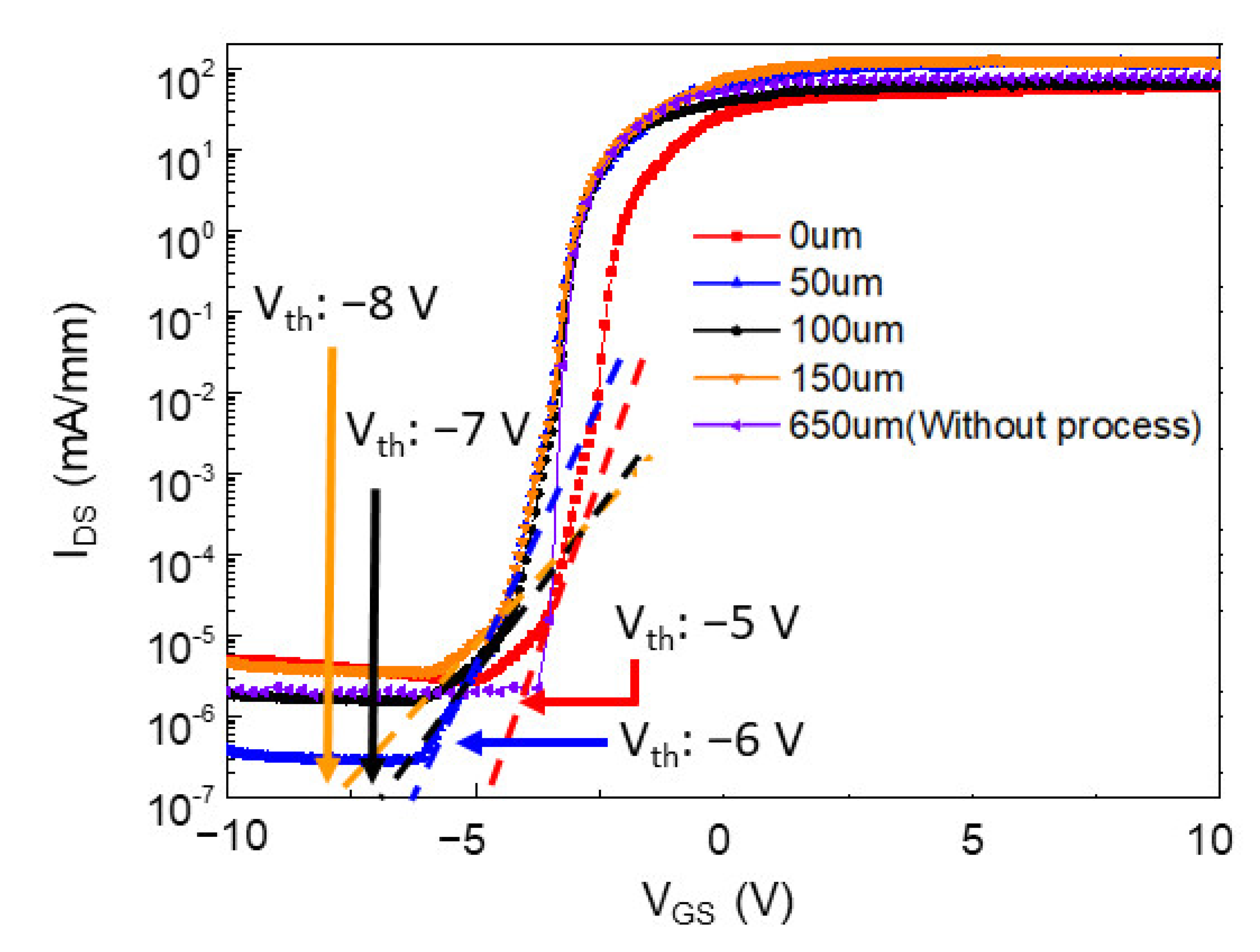
3.2. Impact of BSP on Thermal Dissipation in HEMT Devices

To study the effect of BSP on HEMT heat dissipation, temperature measurements for the above samples were performed at VDS from 0 to 210 V at VGS 0 V. The temperature as a function of input power is shown in Figure 6. The surface temperature was observed to increase owing to channel self-heating with increasing applied power for all devices. The device on 150 µm thick Si substrate without Cu presented the highest surface temperature. In this case, the surface temperature increased to 105.1 °C at 1300 mW. Correspondingly, the thin film HEMT with a Cu substrate presented the lowest surface temperature as Cu has a high thermal conductivity (Table 1). Here, the surface temperature only reached (approx.) 55 °C. This indicates an obvious improvement in heat dissipation after Cu electroplating. In addition, when comparing the four electroplated samples with different Si thicknesses, it was observed that under the same input power, the surface temperature gradually decreases as the Si substrate becomes thinner, until the surface temperature reaches a minimum after substrate removal. Moreover, the slopes of the temperature–power relation for devices on Si substrate with 100 µm and 150 µm thickness plated with 50 µm thick Cu were similar. One possibility is that heat dissipation was impeded by Si being too thick, even though the device temperature on 150 μm Si was higher than that on 100 µm substrate material as power increased to >1100 mW. This suggests that substrate thinning can also improve heat dissipation efficiency. In any case, since Cu is an excellent thermal conductor, electroplating Cu on the device backside aids homogeneous heat distribution, thereby reducing overall device temperature.

3.3. Raman Spectra of HEMT Devices with and without Electroplated Cu

It was expected that Cu electroplating would not induce stress on the fabricated devices as processing occurred at room temperature. We performed Raman spectroscopy measurements to observe the degree of change in stress caused by electroplating and its effect on device characteristics. As shown in Figure 7, after the complete removal of the Si substrate and electroplating, the peak position shifts to 566.25 cm−1, suggesting the GaN lattice is under tensile stress as compared with the E2 peak (567 cm−1) of free-standing GaN [46,47]. In addition, we observed the same peak position and almost the same E2 peak with and without Cu electroplating in the case of devices on 100 µm and 150 µm thick Si substrate. This indicates that the GaN/AlGaN epilayer stress was balanced by the Si substrate with electroplated Cu metal. Additionally, for devices on 50 µm thick Si substrate, as well as for devices after complete removal of Si substrate and Cu electroplating, matching peaks were observed. These results suggest that the stress mainly derives from the thick Si substrate. It is well known that it is necessary to control stress for GaN/AlGaN growth on Si substrate. As the Si substrate was reduced, GaN/AlGaN stress could return to its original type, i.e., compressive stress. After electroplating with Cu, GaN stretching becomes more pronounced. Moreover, the existence of the 2DEG in GaN/AlGaN originates from spontaneous and piezoelectric polarization effects. When the Si substrate is gradually thinned, epitaxial stress is gradually controlled by the electroplated Cu. Although electroplating was processed at room temperature, there could exist stress induced by the plating parameters. Tensile stress induced from the electroplated Cu could increase piezoelectric polarization and IDS. The IDS results (Figure 5a) of the epilayer/ Cu configuration depict the smallest values of this study, suggesting there may exist some further issues influencing IDS that shall be clarified through further study. Finally, if Cu plating parameters can be optimized, the stress between GaN and Cu can be controlled in much the same way as GaN and Si; such an approach is currently under investigation to further improve device characteristics.

4. Conclusions

We have established a new process flow apart from conventional local substrate removal methods for HEMT thermal treatment. Besides substrate removal, Cu was electroplated on the sample backside to improve heat dissipation. For devices on 50 μm thick Si substrate with electroplated Cu, significant improvements in leakage current were observed; the Ion/Ioff ratio increased from 9.61 × 10⁵ to 4.03 × 10⁸. When the Si substrate was <50 μm including the use of Cu, the surface temperature was reduced to 55 °C at a device operating power of 1300 mW. It was also observed that substrate thinning contributes to stress relief while stress from Cu may still affect device performance. These results suggest that substrate thinning and Cu electroplating can be an efficient way to improve heat dissipation and enhance the performance of AlGaN/GaN−based devices.

Author Contributions

R.-H.H.: conceptualization, validation, supervision, project administration, funding acquisition, writing—review and editing. H.-Y.Y.: conceptualization, investigation. N.T.: formal analysis, validation, writing—review and editing. All authors have read and agreed to the published version of the manuscript.

Funding

This study was financially supported by the National Science and Technology Council, Taiwan, under contract No. 111−2622−8−A49−018−SB, 110−2224−E−A49−003, 109−2221−E−009−143−MY3, 111−2923−E−A49−003−MY3.

Data Availability Statement

Data will be made available on request.

Acknowledgments

We thank the Center for Emergent Functional Matter Science of National Chiao Tung University from the Featured Areas Research Center Program within the framework of the Higher Education Sprout Project by the Ministry of Education in Taiwan. We also thank Taiwan Semiconductor Research Institute (TSRI) for the use of their equipment.

Conflicts of Interest

The authors declare that they have no known competing financial interests or personal relationships that could have appeared to influence the work reported in this paper.

References

  1. Vetury, R.; Zhang, N.Q.; Keller, S.; Mishra, U.K. The impact of surface states on the DC and RF characteristics of AlGaN/GaN HFETs. IEEE Trans. Electron Devices 2001, 48, 560–566. [Google Scholar] [CrossRef]
  2. Trew, R.J.; Shin, M.W.; Gatto, V. Wide bandgap semiconductor electronic devices for high frequency applications. In Proceedings of the GaAs IC Symposium IEEE Gallium Arsenide Integrated Circuit Symposium 18th Annual Technical Digest, Orlando, FL, USA, 3–6 November 1996; pp. 6–9. [Google Scholar]
  3. Hudgins, J.; Simin, G.; Santi, E.; Khan, M. An assessment of wide bandgap semiconductors for power devices. IEEE Trans. Power Electron. 2003, 18, 907–914. [Google Scholar] [CrossRef]
  4. Nakamura, S.; Senoh, M.; Nagahama, S.-I.; Iwasa, N.; Yamada, T.; Matsushita, T.; Kiyoku, H.; Sugimoto, Y.; Kozaki, T.; Umemoto, H.; et al. InGaN/GaN/AlGaN-based laser diodes with modulation-doped strained-layer superlattices grown on an epitaxially laterally over-grown GaN substrate. Appl. Phys. Lett. 1998, 72, 211–213. [Google Scholar] [CrossRef]
  5. Khan, A.M.; Kuznia, J.N.; Olson, D.T.; Schaff, W.J.; Burm, J.W.; Shur, M.S. Microwave performance of a 0.25 μm gate AlGaN/GaN heterostructure field effect transistor. Appl. Phys. Lett. 1994, 65, 1121–1123. [Google Scholar] [CrossRef]
  6. Ambacher, O.; Foutz, B.; Smart, J.; Shealy, J.R.; Weimann, N.G.; Chu, K.; Murphy, M.; Sierakowski, A.J.; Schaff, W.J.; Eastman, L.F.; et al. Two-dimensional electron gases induced by spontaneous and piezoelectric polarization in undoped and doped AlGaN/GaN het-erostructures. J. Appl. Phys. 1999, 87, 334–344. [Google Scholar] [CrossRef]
  7. Fletcher, A.A.; Nirmal, D. A survey of Gallium Nitride HEMT for RF and high power applications. Superlattices Microstruct. 2017, 109, 519–537. [Google Scholar] [CrossRef]
  8. Mishra, U.K.; Parikh, P.; Wu, Y.-F. AlGaN/GaN HEMTs-an overview of device operation and applications. Proc. IEEE 2002, 90, 1022–1031. [Google Scholar] [CrossRef]
  9. Levinshtein, M.E.; Rumyantsev, S.L.; Shur, M.S. Properties of Advanced Semiconductor Materials: GaN, AlN, InN, BN, SiC, SiGe; John Wiley & Sons: Hoboken, NJ, USA, 2001. [Google Scholar]
  10. Fletcher, A.A.; Nirmal, D.; Ajayan, J.; Arivazhagan, L. Analysis of AlGaN/GaN HEMT using discrete field plate technique for high power and high frequency applications. AEU Int. J. Electron. Commun. 2018, 99, 325–330. [Google Scholar] [CrossRef]
  11. Wang, Z. Proposal of a novel recess-free enhancement-mode AlGaN/GaN HEMT with field-assembled structure: A simulation study. J. Comput. Electron. 2019, 18, 1251–1258. [Google Scholar] [CrossRef]
  12. Wang, P.; Deng, C.; Cheng, H.; Cheng, W.; Du, F.; Tang, C.; Geng, C.; Tao, N.; Wang, Q.; Yu, H. Simulation of High Breakdown Voltage, Improved Current Collapse Suppression, and Enhanced Frequency Response AlGaN/GaN HEMT Using a Double Floating Field Plate. Crystals 2023, 13, 110. [Google Scholar] [CrossRef]
  13. Wang, Z.; Wang, Z.; Zhang, Z.; Yang, D.; Yao, Y. On the Baliga’s Figure-Of-Merits (BFOM) Enhancement of a Novel GaN Nano-Pillar Vertical Field Effect Transistor (FET) with 2DEG Channel and Patterned Substrate. Nanoscale Res. Lett. 2019, 14, 128. [Google Scholar] [CrossRef] [PubMed]
  14. Pan, S.; Feng, S.; Li, X.; Bai, K.; Lu, X.; Zhu, J.; Zhang, Y.; Zhou, L. Identification of Traps in p-GaN Gate HEMTs During OFF-State Stress by Current Transient Method. IEEE Trans. Elec. Dev. 2022, 69, 4877–4882. [Google Scholar] [CrossRef]
  15. Fernández, E.F.; Ferrer-Rodríguez, J.P.; Almonacid, F.; Pérez-Higueras, P. Current-voltage dynamics of multi-junction CPV modules under different irradiance levels. Sol. Energy 2017, 155, 39–50. [Google Scholar] [CrossRef]
  16. Aguilar-Jiménez, J.A.; Velázquez, N.; Acuña, A.; López-Zavala, R.; González-Uribe, L.A. Effect of orientation of a CPC with concentric tube on efficiency. Appl. Therm. Eng. 2018, 130, 221–229. [Google Scholar] [CrossRef]
  17. Theristis, M.; Fernández, E.F.; Sumner, M.; O’Donovan, T.S. Multiphysics modelling and experimental validation of high concentration photovoltaic modules. Energy Convers. Manag. 2017, 139, 122–134. [Google Scholar] [CrossRef]
  18. Vitanov, S.; Palankovski, V.; Maroldt, S.; Quay, R. High-temperature modeling of AlGaN/GaN HEMTs. Solid-State Electron. 2010, 54, 1105–1112. [Google Scholar] [CrossRef]
  19. Wang, X.-D.; Hu, W.-D.; Chen, X.-S.; Lu, W. The Study of Self-Heating and Hot-Electron Effects for AlGaN/GaN Double-Channel HEMTs. IEEE Trans. Electron Devices 2012, 59, 1393–1401. [Google Scholar] [CrossRef]
  20. Saidi, I.; Gassoumi, M.; Maaref, H.; Mejri, H.; Gaquière, C. Self-heating and trapping effects in AlGaN/GaN heterojunction field-effect transistors. J. Appl. Phys. 2009, 106, 054511. [Google Scholar] [CrossRef]
  21. Turin, V.; Balandin, A. Performance degradation of GaN field-effect transistors due to thermal boundary resistance at GaN∕substrate interface. Electron. Lett. 2004, 40, 81–83. [Google Scholar] [CrossRef]
  22. Goyal, V.; Subrina, S.; Nika, D.L.; Balandin, A.A. Reduced thermal resistance of the silicon-synthetic diamond composite substrates at elevated temperatures. Appl. Phys. Lett. 2010, 97, 031904. [Google Scholar] [CrossRef]
  23. Slack, G.A. Thermal Conductivity of Pure and Impure Silicon, Silicon Carbide, and Diamond. J. Appl. Phys. 1964, 35, 3460–3466. [Google Scholar] [CrossRef]
  24. Kidalov, S.V.; Shakhov, F.M. Thermal Conductivity of Diamond Composites. Materials 2009, 2, 2467–2495. [Google Scholar] [CrossRef]
  25. Sun, J.; Fatima, H.; Koudymov, A.; Chitnis, A.; Hu, X.; Wang, H.-M.; Zhang, J.; Simin, G.; Yang, J.; Khan, M.A.; et al. Thermal management of AlGaN-GaN HFETs on sapphire using flip-chip bonding with epoxy underfill. IEEE Electron Device Lett. 2003, 24, 375–377. [Google Scholar] [CrossRef]
  26. Hiroki, M.; Kumakura, K.; Kobayashi, Y.; Akasaka, T.; Makimoto, T.; Yamamoto, H. Suppression of self-heating effect in AlGaN/GaN high electron mobility transistors by substrate-transfer technology using h-BN. Appl. Phys. Lett. 2014, 105, 193509. [Google Scholar] [CrossRef]
  27. Ji, H.; Das, J.; Germain, M.; Kuball, M. Laser lift-off transfer of AlGaN/GaN HEMTs from sapphire onto Si: A thermal perspective. Solid-State Electron. 2009, 53, 526–529. [Google Scholar] [CrossRef]
  28. Tadjer, M.J.; Anderson, T.J.; Hobart, K.D.; Feygelson, T.I.; Caldwell, J.D.; Eddy, C.R.; Kub, F.J.; Butler, J.E.; Pate, B.; Melngailis, J. Reduced Self-Heating in AlGaN/GaN HEMTs Using Nanocrystalline Diamond Heat-Spreading Films. IEEE Electron. Device Lett. 2011, 33, 23–25. [Google Scholar] [CrossRef]
  29. Tadjer, M.J.; Anderson, T.J.; Feygelson, T.I.; Hobart, K.D.; Hite, J.K.; Koehler, A.D.; Wheeler, V.D.; Pate, B.B.; Eddy, C.R.; Kub, F.J. Nanocrystalline diamond capped AlGaN/GaN high electron mobility transistors via a sacrificial gate process. Phys. Status Solidi A 2016, 213, 893–897. [Google Scholar] [CrossRef]
  30. Srivastava, P.; Das, J.; Visalli, D.; Van Hove, M.; Malinowski, P.E.; Marcon, D.; Lenci, S.; Geens, K.; Cheng, K.; Leys, M.; et al. Record Breakdown Voltage (2200 V) of GaN DHFETs on Si With 2-μm Buffer Thickness by Local Substrate Removal. IEEE Electron. Device Lett. 2011, 30, 30–32. [Google Scholar] [CrossRef]
  31. Visalli, D.; Van Hove, M.; Derluyn, J.; Srivastava, P.; Marcon, D.; Das, J.; Leys, M.R.; Degroote, S.; Cheng, K.; Vandenplas, E.; et al. Limitations of Field Plate Effect Due to the Silicon Substrate in AlGaN/GaN/AlGaN DHFETs. IEEE Trans. Electron. Devices 2010, 57, 3333–3339. [Google Scholar] [CrossRef]
  32. Pavlidis, G.; Kim, S.H.; Abid, I.; Zegaoui, M.; Medjdoub, F.; Graham, S. The Effects of AlN and Copper Back Side Deposition on the Performance of Etched Back GaN/Si HEMTs. IEEE Electron. Device Lett. 2019, 40, 1060–1063. [Google Scholar] [CrossRef]
  33. Shin, Y.; Kim, S.E.; Kim, S. Thermal assessment of copper through silicon via in 3D IC. Microelectron. Eng. 2016, 156, 2–5. [Google Scholar] [CrossRef]
  34. Lau, J.H.; Yue, T.G. Thermal management of 3D IC integration with TSV (through silicon via). In Proceedings of the IEEE 59th Electronic Components and Technology Conference, San Diego, CA, USA, 26–29 May 2009; pp. 635–640. [Google Scholar]
  35. Hsueh, K.-P.; Wang, H.-Y.; Wang, H.-C.; Kao, H.-L.; Chien, F.-T.; Chen, C.-T.; Chang, K.-J.; Chiu, H.-C. Reliability Studies on AlGaN/GaN Metal-Insulator-Semiconductor High-Electron-Mobility Transistors with Through-Substrate via Technique and Backside Heat Sink Metal on Silicon-on-Insulator Substrates. ECS J. Solid State Sci. Technol. 2018, 7, Q142–Q147. [Google Scholar] [CrossRef]
  36. Hwang, Y.-H.; Kang, T.-S.; Ren, F.; Pearton, S.J. Novel approach to improve heat dissipation of AlGaN/GaN high electron mobility transistors with a Cu filled via under device active area. J. Vac. Sci. Technol. B 2014, 32, 061202. [Google Scholar] [CrossRef]
  37. Jang, K.-W.; Hwang, I.-T.; Kim, H.-J.; Lee, S.-H.; Lim, J.-W.; Kim, H.-S. Thermal Analysis and Operational Characteristics of an AlGaN/GaN High Electron Mobility Transistor with Copper-Filled Structures: A Simulation Study. Micromachines 2019, 11, 53. [Google Scholar] [CrossRef]
  38. Mohanty, S.K.; Chen, Y.Y.; Yeh, P.H.; Horng, R.H. Thermal Management of Gan-on-Si High electron Mobility transistor by copper filled Mi-cro-trench Structure. Sci. Rep. 2019, 9, 19691. [Google Scholar] [CrossRef]
  39. Abid, I.; Canato, E.; Meneghini, M.; Meneghesso, G.; Cheng, K.; Medjdoub, F. GaN-on-silicon transistors with reduced current collapse and improved blocking voltage by means of local substrate removal. Appl. Phys. Exp. 2021, 14, 036501. [Google Scholar] [CrossRef]
  40. Dogmus, E.; Zegaoui, M.; Medjdoub, F. GaN-on-silicon high-electron-mobility transistor technology with ultra-low leakage up to 3000 V using local substrate removal and AlN ultra-wide bandgap. Appl. Phys. Exp. 2018, 11, 034102. [Google Scholar] [CrossRef]
  41. Malakoutian, M.; Ren, C.; Woo, K.; Li, H.; Chowdhury, S. Development of Polycrystalline Diamond Compatible with the Latest N-Polar GaN mm-Wave Technology. Cryst. Growth Des. 2021, 21, 2624–2632. [Google Scholar] [CrossRef]
  42. Guo, H.; Li, Y.; Yu, X.; Zhou, J.; Kong, Y. Thermal Performance Improvement of AlGaN/GaN HEMTs Using Nanocrystalline Diamond Capping Layers. Micromachines 2022, 13, 1486. [Google Scholar] [CrossRef] [PubMed]
  43. Nittala, P.V.K.; Remesh, N.; Niranjan, S.; Tasneem, S.; Raghavan, S.; Muralidharan, R.; Nath, D.N.; Sen, P. Enabling Transfer of Ultrathin Layers of GaN for Demonstration of a Heterogenous Stack on Copper Heat Spreader. IEEE Trans. Compon. Packag. Manuf. Technol. 2019, 10, 339–342. [Google Scholar] [CrossRef]
  44. Zhao, M.; Tang, X.; Huo, W.; Han, L.; Deng, Z.; Jiang, Y.; Wang, W.; Chen, H.; Du, C.; Jia, H. Characteristics of AlGaN/GaN high electron mobility transistors on metallic substrate. Chin. Phys. B 2020, 29, 048104. [Google Scholar] [CrossRef]
  45. Wang, Z.; Li, L.; Yao, Y. Machine Learning-Assisted Model for GaN Ohmic Contacts Regarding Fabrication Procesces. IEEE Trans. Electron. Devices 2021, 68, 2212–2219. [Google Scholar] [CrossRef]
  46. Konenkova, E.V.; Fedirko, V.A.; Zahn, D.R.; Zhilyaev, Y.V. Raman spectroscopy of GaN nucleation and free-standing layers grown by hydride vapor phase epitaxy on oxidized silicon. Appl. Phys. Lett. 2003, 83, 629–631. [Google Scholar] [CrossRef]
  47. Sun, H.; Liu, D.; Pomeroy, J.W.; Francis, D.; Faili, F.; Twitchen, D.J.; Kuball, M. GaN-on-diamond: Robust mechanical and thermal properties. In Proceedings of the CS Man-Tech Conference, Miami, FL, USA, 16–19 May 2016; pp. 201–204. [Google Scholar]
Figure 1. Flowchart of fabrication of heterostructure HEMT device: (a) device structure, (b) mesa etching using ICPRIE, (c) deposition source (S) and drain (D) electrodes, (d) Al2O3 gate oxide layer deposition, (e) deposition of gate electrode, then SiNx as a passivation layer and open S, D, G electrodes, and (f) optical microscope image of the fabricated HEMT device.
Electronics 12 02033 g001
Figure 2. Process flowchart of backside heat dissipation structure: (a) device facing down, (b) device side bonded to sapphire using a template adhesive layer, (c) reducing Si substrate to 150 µm by grinding and chemical etching, (d) seed layer using Cr/Au deposition, (e) electroplating the Cu permanent substrate, (f) removing the carrier substrate (sapphire), (g) face-up view of the final device and (h) face-down view of the final substrate.
Electronics 12 02033 g002
Figure 3. IDS and |IGS| as functions of VGS of HEMT device before and after Cu plating substrates (a) after complete removal of Si substrate and with (b) 50 μm, (c) 100 µm and (d) 150 µm of Si substrate.
Electronics 12 02033 g003
Figure 4. IDS−VGS device characteristics with Cu plating on different Si substrate thicknesses as compared with those of original sample.
Electronics 12 02033 g004
Figure 5. ID−VDS characteristics before and after BSP: (a) complete removal of silicon substrate; (b) 50 μm, (c) 100 μm and (d) 150 μm thick silicon substrate with electroplating of 50μm thick copper in each case.
Electronics 12 02033 g005
Figure 6. Temperature as a function of power for HEMT devices with different Si substrate thicknesses.
Electronics 12 02033 g006
Figure 7. Raman spectra of GaN E2 peak.
Electronics 12 02033 g007
Table 1. Thermal conductivity and thermal expansion coefficients of Si and Cu.
MaterialSiCu
Thermal conductivity coefficient (W/m.K)135386
Thermal expansion coefficient (1/K) × 10−62.616.7
Disclaimer/Publisher’s Note: The statements, opinions and data contained in all publications are solely those of the individual author(s) and contributor(s) and not of MDPI and/or the editor(s). MDPI and/or the editor(s) disclaim responsibility for any injury to people or property resulting from any ideas, methods, instructions or products referred to in the content.

