Article

Analysis of DC-Side Snubbers for SiC Devices Application

School of Electrical and Control Engineering, North China University of Technology, Beijing 100144, China
*
Authors to whom correspondence should be addressed.
Electronics 2022, 11(23), 3874; https://doi.org/10.3390/electronics11233874
Submission received: 12 October 2022 / Revised: 10 November 2022 / Accepted: 20 November 2022 / Published: 23 November 2022
(This article belongs to the Special Issue Wide Bandgap Semiconductor: From Epilayer to Devices)

Abstract

:
Due to parasitic parameters existing in Silicon Carbide (SiC) devices application, SiC devices have poor turn-off performances. SiC diode and SiC MOSFET have severe turn-off overvoltage and oscillation. The DC-side snubber is one simple suppressing method. The simplest circuit is the high-frequency decoupling capacitor in parallel with the bridge leg. However, choosing the component value is empirical. Based on the turn-off terminal impedances of the SiC diode and the SiC MOSFET, the suppressing mechanism of this DC-side snubber is analyzed. The guideline selection for the component value is provided. Furthermore, the DC-side snubber with a damping resistor is analyzed based on the terminal impedances. The design principles are provided. Finally, the validity and effectiveness of the DC-side snubbers were proven based on the double-pulse test platform.

1. Introduction

In recent years, Silicon Carbide (SiC) devices have emerged as a kind of promising candidates for high-performance power conversion [1,2]. Compared with state-of-the-art silicon devices, they are featured with higher switching speeds and lower switching loss [3,4]. Therefore, the switching frequency of the power electronic equipment with SiC devices has been continuously pushed up to reduce the size of passive components, which realizes the high-power density [5,6]. However, due to parasitic parameters existing in SiC devices application, SiC devices have poor turn-off performances [7]. SiC diode and SiC MOSFET will have severe turn-off overvoltage and oscillation [8,9]. To avoid damaging the devices, the voltage rating must be enough, which will increase the system cost [10,11,12].
The turn-off terminal impedance is used to analyze the mechanism of the turn-off voltage and oscillation of the SiC MOSFET [13,14]. The parasitic capacitors of the SiC MOSFET and the loop parasitic inductors resonate, which amplifies the component of the excitation source and results in the turn-off overvoltage and oscillation [15,16]. The turn-off terminal impedance analysis method can be performed to provide the suppressing guidelines.
The suppressing methods for the turn-off overvoltage and oscillation on devices can be classified into two categories. One method is to reduce the switching speed of devices, which can be implemented by increasing the gate resistor. However, poor switching performances will be attained, including the switching delay time and the switching loss [17,18]. Another method is to add snubbers to the circuit. One type of snubber is connected directly to the devices, such as the R¬–C snubber [19,20] and the R–C–D snubber [21,22]. By these device snubbers, the turn-off overvoltage can be decreased, but the turn-on overcurrent and the loss can be increased. Furthermore, the suppressing effectiveness can be weakened by the added parasitic inductors owning to device snubbers. Therefore, device snubbers are used less in high-speed SiC devices application. Another type of snubber is the DC-side snubber, which is one simple suppressing method. The simplest circuit is the high-frequency decoupling capacitor in parallel with the bridge leg [23]. By DC-side snubbers, a portion of parasitic inductors can be decoupled from the switching power loop. However, choosing the component value is empirical. Moreover, the suppressing effectiveness is not good when the bulk of the decoupling capacitor leads large parasitic inductors to the switching power loop. In a silicon IGBT application, a damping resistor is in series with the high-frequency decoupling capacitor to suppress the turn-off overvoltage [24]. However, the effectiveness will be decreased if parameters are not designed appropriately. Another DC-side snubber in [25] is the high-frequency decoupling capacitor in parallel with the capacitor-damping-resistor branch. The capacitor-damping-resistor branch is used to suppress the low-frequency oscillation on the turn-off voltage. Nevertheless, the low-frequency oscillation cannot be fully eliminated.
Based on previous considerations, this paper aims to design an effective DC-side snubber to suppress the turn-off overvoltage and oscillation for SiC devices application. One contribution from this paper is that the turn-off terminal impedances of the SiC diode and the SiC MOSFET were deduced. By these turn-off terminal impedances, the suppressing mechanisms and design principles of DC-side snubbers can be investigated. Another contribution of this paper is the guideline design for the DC-side snubbers is presented, which can provide the theoretical, not the empirical, design.
The rest of this paper is organized as follows. First, the suppressing mechanism of the simplest DC-side snubber is discussed in detail. Then, the DC-side snubber with the damping resistor is analyzed. Finally, the validity and effectiveness of the DC-side snubbers are verified by experimental results.

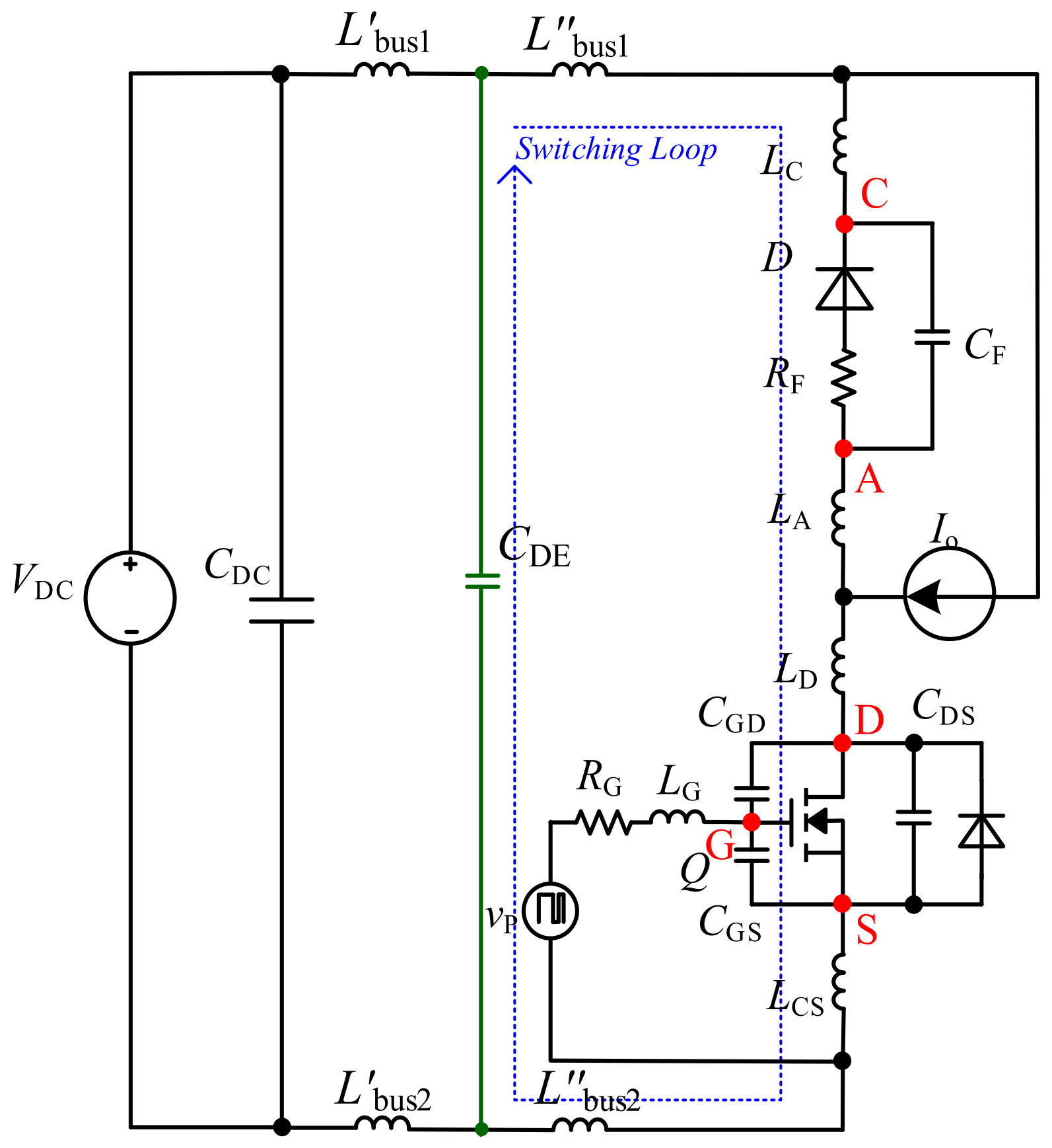
2. Suppressing Mechanism of DC-Side Snubber CDE

In a phase-leg configuration, such as boost, buck-boost, half-bridge, and full-bridge, the active switch makes current communication with the freewheeling diode during the turn-on and turn-off transition of the active switch. The basic cell is shown in Figure 1, with one branch being the output current, Io, one branch being the freewheeling diode, and one branch being the active switch, which was chosen to study. The input voltage source, VDC, is constant. The output current, Io, is constant. CDC is the DC bulk capacitor. CDE is the DC-side snubber capacitor. The switch, Q, is driven by the double pulse signal. The switching of Q causes current commutation with the external circuit and the diode, D. However, the parasitic elements existing in the circuit need to be considered due to the high-speed switching SiC MOSFET. The parasitic elements in Figure 1 are the gate–source capacitance (CGS), the gate–drain capacitance (CGD), the drain–source capacitance (CDS), the gate inductance (LG), the drain inductance (LD), the source inductance (LS) of the Q and the junction capacitance (CF), the cathode inductance (LC1), and the anode inductance (LA1) of the diode (D). A SiC diode is employed as the freewheeling diode, which does not have the reverse recovery charge (Qrr) and has a low voltage drop. Lbus1, Lbus2, L′′bus1, and L′′bus2 represent the interconnection parasitic inductors of the PCB traces. LCS are the common source inductances shared by the switching power loop and the gate drive loop. RG represents the external gate drive resistance. vP is the gate signal for the SiC MOSFET.
The turn-on switching transition of the SiC MOSFET can be divided into four stages [26], which are the Turn-on Delay Time (Stage 1: t1t2), Current Rising Time (Stage 2: t2t3), Voltage Falling Time (Stage 3: t3t4), and Gate Remaining Charging Time (Stage 4: t4t5). The turn-off switching transition of the SiC MOSFET can be divided into four stages [26], which are the Turn-off Delay Time (Stage 5: t5t6), Voltage Rising Time (Stage 6: t6t7), Current Falling Time (Stage 7: t7t8), and Gate Remaining Discharging Time (Stage 8: t8t9). Figure 2 shows the switching waveforms of the SiC diode and the SiC MOSFET. During Stage 4, the turn-off overvoltage and oscillation of the SiC diode occur. During Stage 7 and Stage 8, the turn-off overvoltage and oscillation of the SiC MOSFET occur.

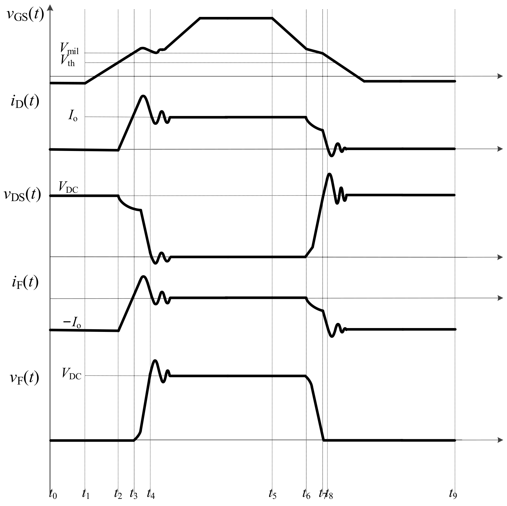
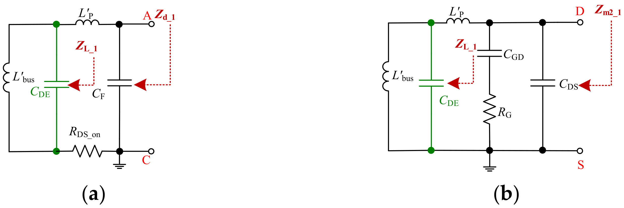
2.1. Analysis of Stage 4

At t4, the voltage of the SiC diode, vF, reaches the input voltage, VDC. Then the turn-off overvoltage and oscillation on the SiC diode occurs. In this stage, the SiC MOSFET is equivalent to the on-state resistor (RDS_on). Figure 3a shows the equivalent circuit at this stage, in which LP is the sum of LC, LA, LD, LCS, L′′bus1, and L′′bus2. Lbus is the sum of Lbus1 and Lbus2. The parasitic capacitors of the SiC MOSFET are neglected because the SiC MOSFET is in the on-state. The terminal impedance Zd_1 is calculated as Equation (1), as the following,
Z d _ 1 ( s ) = N d _ 1 s D d _ 1 s ,
where Nd_1(s) and Dd_1(s) are shown in Appendix A. The amplitude–frequency curves of the terminal impedance Zd_1 are shown in Figure 4a, based on the parameters in Table 1. To be consistent with the experimental verification in Section 4, parameters of the SiC MOSFET C2M0080120D and the SiC diode C4D20120A were used. Based on Figure 4a, there are two resonant peaks existing on the terminal impedance Zd_1. The resonant frequencies are expressed as Equations (2) and (3),
f d _ 1 _ 1 1 2 π L P C D E C F C D E + C F ,
f d _ 1 _ 2 1 2 π L b u s C D E + C F ,
where fd_1_1 represents the high-resonance frequency of the terminal impedance Zd_1, and fd_1_2 represents the low-resonance frequency of the terminal impedance Zd_1. The peak resonant impedances of the terminal impedance Zd_1 amplify the excitation source at the resonant frequencies and result in two oscillations overlaying on the turn-off voltage of the SiC diode.

2.2. Analysis of Stage 7 and Stage 8

At t7, the SiC diode and the SiC MOSFET make a current commutation, and the turn-off overvoltage of the SiC MOSFET occurs. At t8, the current commutation comes to an end, and the oscillation on the turn-off voltage of the SiC MOSFET occurs. Figure 3b shows the equivalent circuit at these two stages. The capacitor of the SiC diode is neglected because the SiC diode is in the on-state. The terminal impedance Zm2_1 is calculated as Equation (4),
Z m 2 _ 1 ( s ) = N m 2 _ 1 s D m 2 _ 1 s ,
where Nm2_1(s) and Dm2_1(s) are shown in Appendix A. The amplitude–frequency curves of the terminal impedance, Zm2_1, are based on the parameters in Table 1, as shown in Figure 4b. In Figure 4b, there are two resonant peaks existing on the terminal impedance Zm2_1, which is the same as the terminal impedance Zd_1. The resonant frequencies are expressed as Equations (2) and (3),
f m 2 _ 1 _ 1 1 2 π L P C DE C oss C DE + C oss ,
f m 2 _ 1 _ 2 1 2 π L bus C DE + C oss ,
where fm2_1_1 represents the high-resonance frequency of the terminal impedance Zm2_1 and fm2_1_2 represents the low-resonance frequency of the terminal impedance Zm2_1, and Coss = CGD + CDS. The peak resonant impedances of the terminal impedance Zm2_1 amplify the excitation source at the resonant frequencies and result in two oscillations overlaying on the turn-off voltage of the SiC MOSFET.

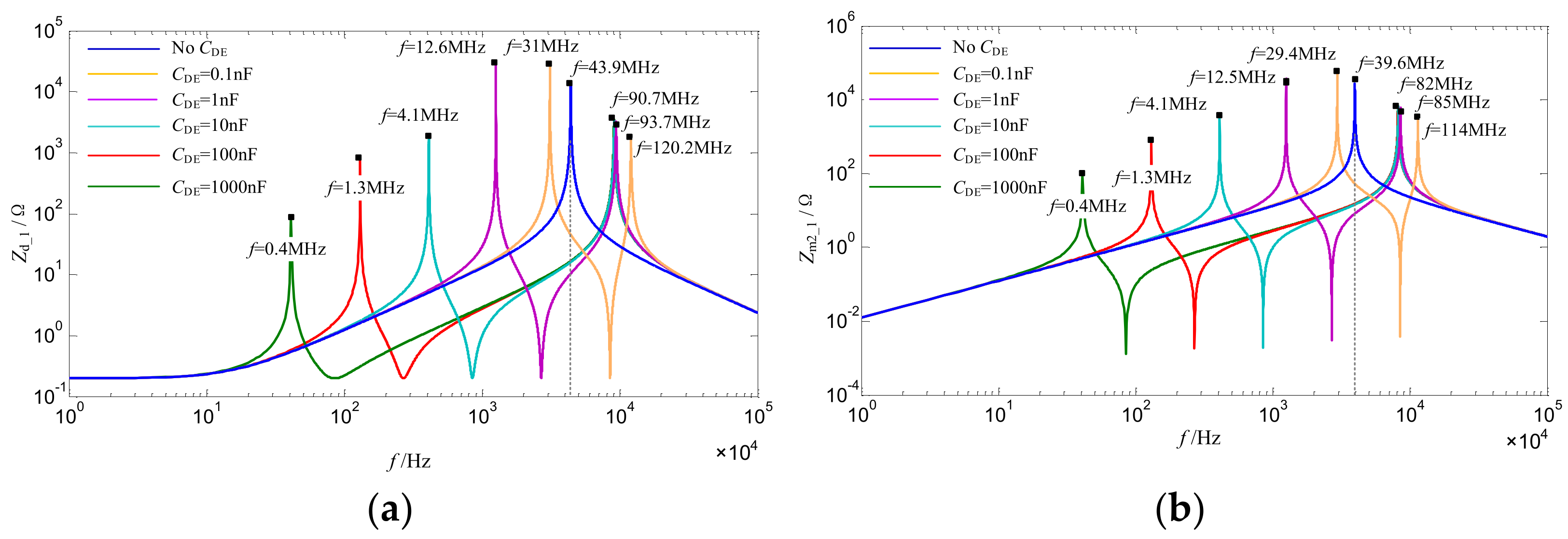
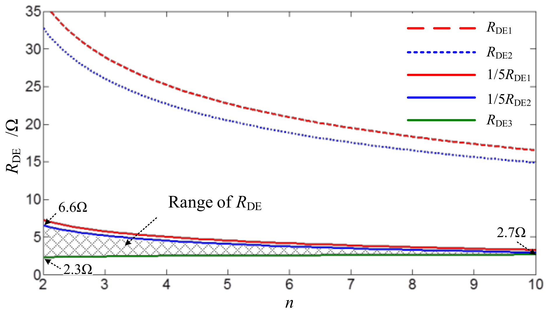
2.3. Guideline Selection for Capacitor CDE

To realize the decouple of the inductor Lbus from the switching power loop and make inductor Lbus and parasitic capacitors CF, CGD, and CDS no resonance, capacitor CDE must be much larger than the parasitic capacitors CF, CGD, and CDS according to Equations (1)–(6). In addition, the impedance ZL_1 of the paralleling branches Lbus and CDE at the high-resonance frequency fd1_1_1 and the high-resonance frequency fm2_1_1 should be much lower than the impedance of inductor LP. In general, the capacitor CDE satisfies the inequality in Equation (7). It is considered that capacitor CDE is large enough than parasitic capacitors CF, CGD, and CDS.
C DE max ( 100 C o s s , 100 C F ) .
The impedance ZL_1 of the paralleling branches Lbus and CDE can be expressed as Equation (8). In addition, Equation (9) should be satisfied and simplified as Equation (10).
Z L _ 1 ( s ) = L bus s C DE L bus s 2 + 1 .
j 2 π f d _ 1 _ 1 L P j 2 π f d _ 1 _ 1 L bus ( j 2 π f d _ 1 _ 1 ) 2 C DE L bus + 1 j 2 π f m 2 _ 1 _ 1 L P j 2 π f m 2 _ 1 _ 1 L bus ( j 2 π f m 2 _ 1 _ 1 ) 2 C DE L bus + 1 .
Assuming that Lbus = nLP. Equation (9) can be simplified as Equation (10),
C DE max 1 + 1 n C F , 1 + 1 n C oss .
As simplified steps of Equation (7), Equation (11) represents that capacitor CDE satisfies Equation (10).
C DE max 100 1 + 1 n C F , 100 1 + 1 n C oss .
In Figure 4, capacitor CDE is set to none, 0.1 nF, 1 nF, 10 nF, 100 nF, and 1000 nF, respectively. When capacitor CDE is larger than 10nF, the peak impedances on the terminal impedances, Zd_1 and Zm2_1, are obviously smaller than without the capacitor CDE. In addition, the high-resonance frequencies are scarcely affected by capacitor CDE. However, the low-frequency resonances are still affected by the capacitor CDE. Based on Equations (3) and (6), the low-frequency resonances are caused by the capacitor CDE and inductor Lbus. The voltage fluctuation, ∆vCDE, on capacitor CDE can be calculated as Equation (12). Assuming that the limitation of the voltage fluctuation is ∆VCDE, capacitor CDE also needs to satisfy Equation (13).
Δ v CDE = I o L bus C DE sin t L bus C DE .
C DE 4 I o 2 Δ V CDE 2 L bus .
In summary, the DC-side snubber CDE needs to satisfy Equation (14), and the decoupling of the parasitic inductor Lbus and the suppression for the low-frequency oscillation on the turn-off voltage can be realized.
C DE max ( 100 C F , 100 C o s s , 100 1 + 1 n C F , 100 1 + 1 n C oss , 4 I o 2 Δ V CDE 2 L bus ) .

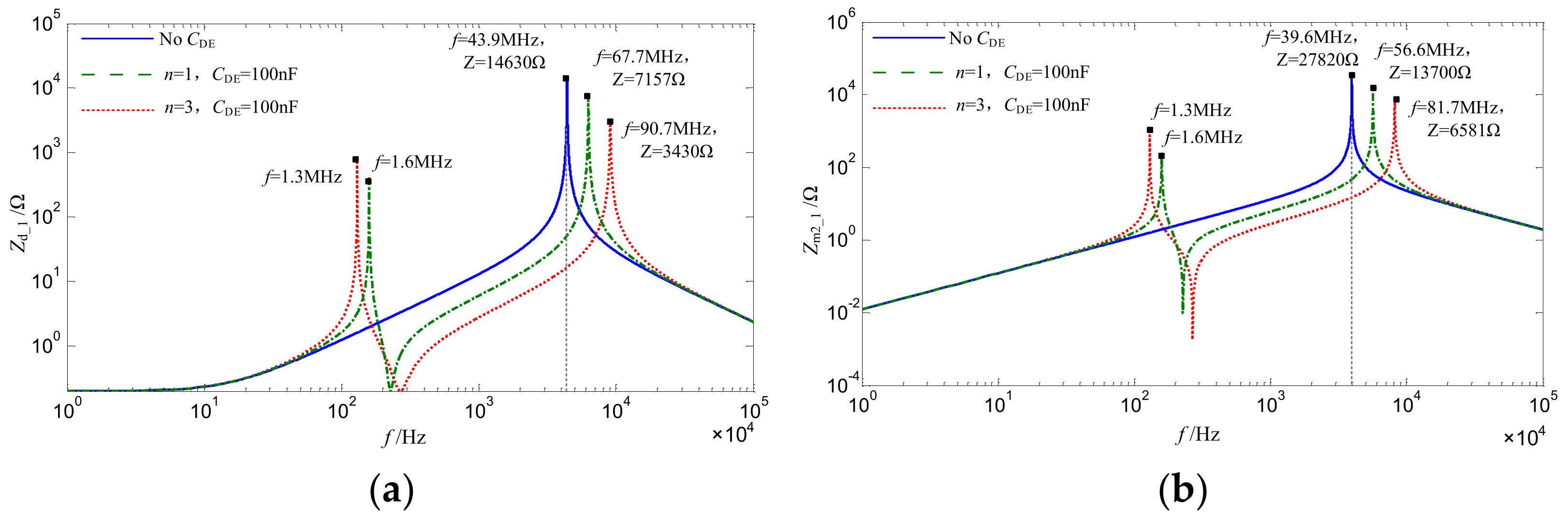
2.4. Analyzation for the Suppressing Effectiveness of Capacitor CDE

Assume the peak impedances, Zd_1_H_P and Zm2_1_H_P, of the SiC diode and SiC MOSFET with the capacitor CDE are 1/ρ times the peak impedances, Zd_H_P and Zm2_H_P, without the capacitor CDE. Equations (15)–(18) express the peak impedances without and with the capacitor CDE.
Z d _ H _ P = L P + L b u s R D S _ o n C F ,
Z m 2 _ H _ P = L P + L b u s C o s s R G C G D 2 ,
Z d _ 1 _ H _ P = L P R D S _ o n C F ,
Z m 2 _ 1 _ H _ P = L P C o s s R G C G D 2 .
Therefore, Equation (19) can be derived based on the relations between the peak impedances Zd_H_P, Zm2_H_P and Zd_1_H_P, Zm2_1_H_P.
ρ n + 1 .
Figure 5 presents the amplitude–frequency curves of terminal impedances, Zd_1 and Zm2_1, with different n values based on parameters in Table 1. Inductors Lbus and LP are set to 50 nH, 150 nH or 100 nH, 100 nH, respectively, which means n = 3 or n = 1. Based on Figure 5, the larger n is, the smaller LP is, which represents that the capacitor CDE is closer to the devices, the lower the peak impedance is. Compared to without CDE, the peak impedance of terminal impedances, Zd_1 and Zm2_1, with CDE is reduced nearly n/(n + 1) times.

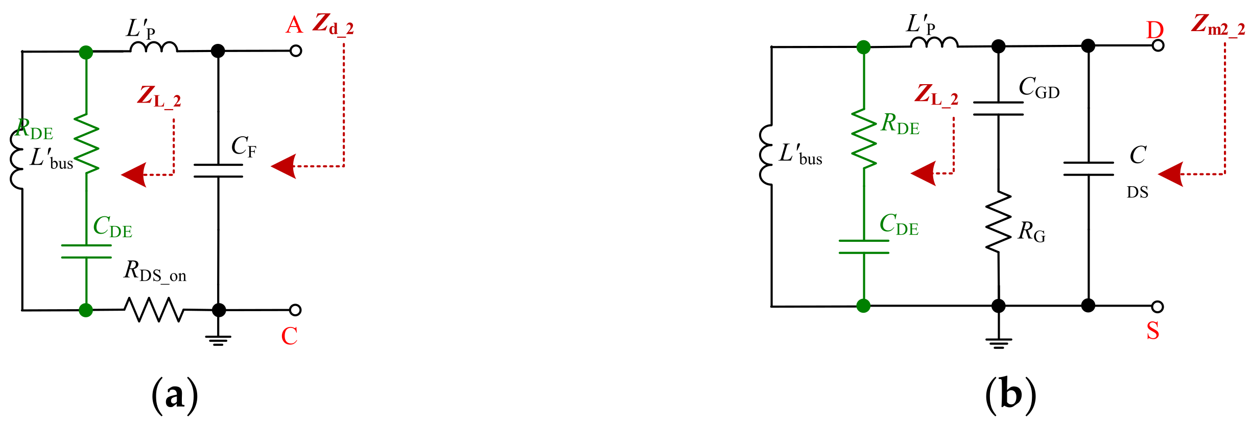
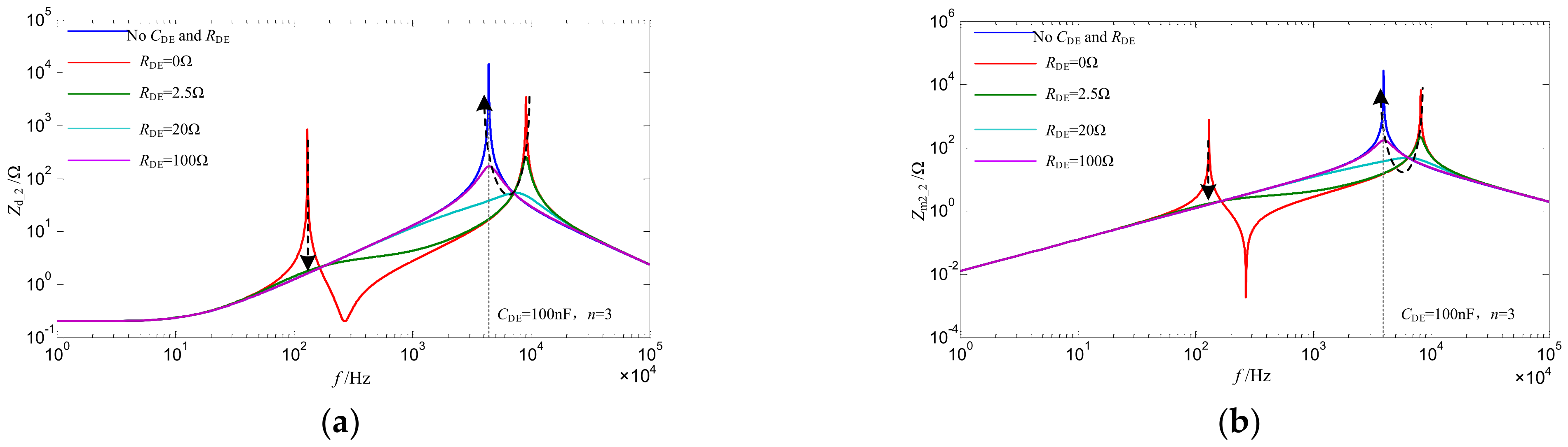
3. Analyzation for DC-Side Snubber with Damping Resistor CDERDE

When the DC-side snubber CDE cannot be selected large enough to avoid the low-frequency oscillation on the turn-off voltage, the suppressing effectiveness is not good owning to the bigger capacitor with parasitic inductors added to the switching power loop. The DC-side snubber with a damping resistor can be used to solve this problem, which is the high-frequency decoupling capacitor in series with a damping resistor. Figure 6 shows the equivalent circuits with this DC-side snubber. Capacitor CDE is to decouple the parasitic inductor Lbus, and resistor RDE is to dampen the low-frequency oscillation on the turn-off voltage.
If capacitor CDE satisfies Equation (7) and Equation (11) and realizes the decoupling of the inductor Lbus from the switching power loop, the low-frequency resonance is only caused by the capacitor CDE and inductor Lbus. The impedance ZL_2 of the paralleling branches Lbus and CDE-RDE can be calculated as Equation (20),
Z L _ 2 ( s ) = ( C DE R DE s + 1 ) L bus s C DE L bus s 2 + C DE R DE s + 1 .
Due to the damping resistor RDE that is in series with capacitor CDE, the impedance ZL_2 at the high-resonance frequency fd1_1_1 and the high-resonance frequency fm2_1_1 should be much lower than the impedance of inductor LP. The relations can be expressed as Equation (21),
j 2 π f d _ 1 _ 1 L P ( j 2 π f d _ 1 _ 1 C DE R DE + 1 ) j 2 π f d _ 1 _ 1 L bus ( j 2 π f d _ 1 _ 1 ) 2 C DE L bus + j 2 π f d _ 1 _ 1 C DE R DE + 1 j 2 π f m 2 _ 1 _ 1 L P ( j 2 π f m 2 _ 1 _ 1 C DE R DE + 1 ) j 2 π f m 2 _ 1 _ 1 L bus ( j 2 π f m 2 _ 1 _ 1 ) 2 C DE L bus + j 2 π f m 2 _ 1 _ 1 C DE R DE + 1 .
Assuming that CDE = m1CF and CDE = m2Coss, Equation (21) can be simplified as
R DE R DE 1 R DE R DE 2 ,
where RDE1 = ((1 − nm1)2n2)/((n2 − 1)(n + 1)m1))1/2((Lbus + LP)/CDE)1/2 and RDE2 = (((1 − nm2)2n2)/((n2 − 1)(n + 1) m2))1/2((Lbus + LP)/CDE)1/2. To reduce the scale of the damping resistor RDE, Equation (22) can be simplified as,
R DE min ( 1 5 R DE 1 , 1 5 R DE 2 ) .
Due to its discriminant of Equation (20), the low-frequency resonances on the terminal impedances, Zd_1 and Zm2_1, of the SiC diode and SiC MOSFET can be cancelled completely when the damping resistor RDE satisfies Equation (24).
R DE R DE 3 ,
where RDE3 = 2(n/(n + 1))1/2((Lbus + LP)/CDE)1/2. According to Equations (23) and (24), Figure 7 shows the range of the damping resistor RDE. The larger n is, the smaller the range of the damping resistor RDE is.
According to Figure 7, the terminal impedances, Zd_2 and Zm2_2, of the SiC diode and SiC MOSFET can be calculated as Equations (25) and (26),
Z d _ 2 ( s ) = N d _ 2 s D d _ 2 s ,
Z m 2 _ 2 ( s ) = N m 2 _ 2 s D m 2 _ 2 s .
where Nd_2(s), Dd_2(s), Nm2_2(s), and Dm2_2(s) are shown in Appendix A. The amplitude–frequency curves of Zd_2 and Zm2_2, based on Table 1, are shown in Figure 8. From Figure 8, the low-frequency peak impedances of Zd_2 and Zm2_2 are eliminated, which indicates this DC-side snubber can effectively suppress the low-frequency oscillation on turn-off voltage. In addition, if resistor RDE satisfies its range requirement, the high-resonance frequency of the terminal impedance, Zd_2 and Zm2_2, is scarcely affected, and the high-frequency peak impedances are reduced. It is indicated that inductor Lbus can be decoupled from the switching power loop, and resistor RDE has suppressing effectiveness on the turn-off overvoltage.

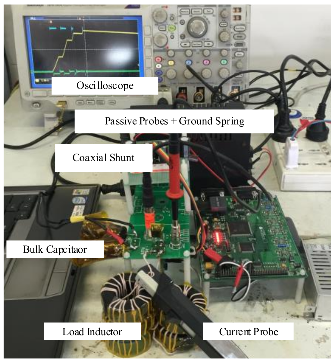
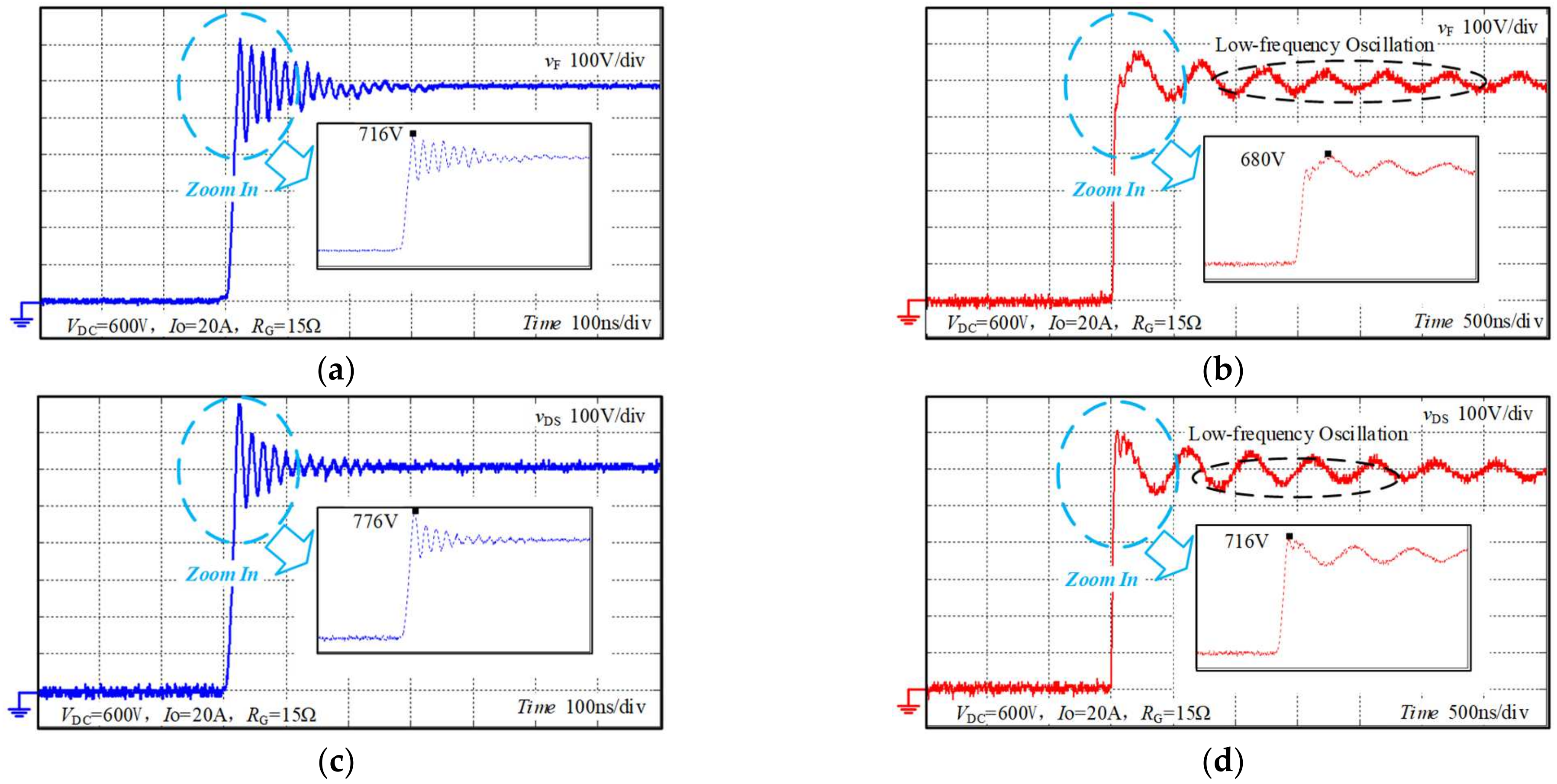
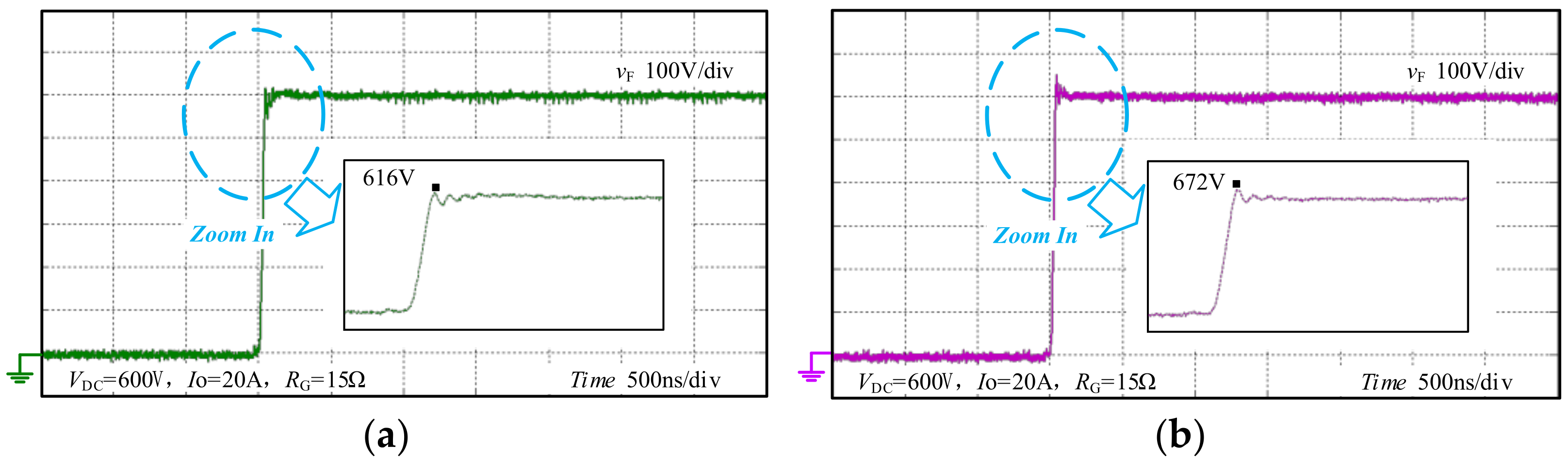
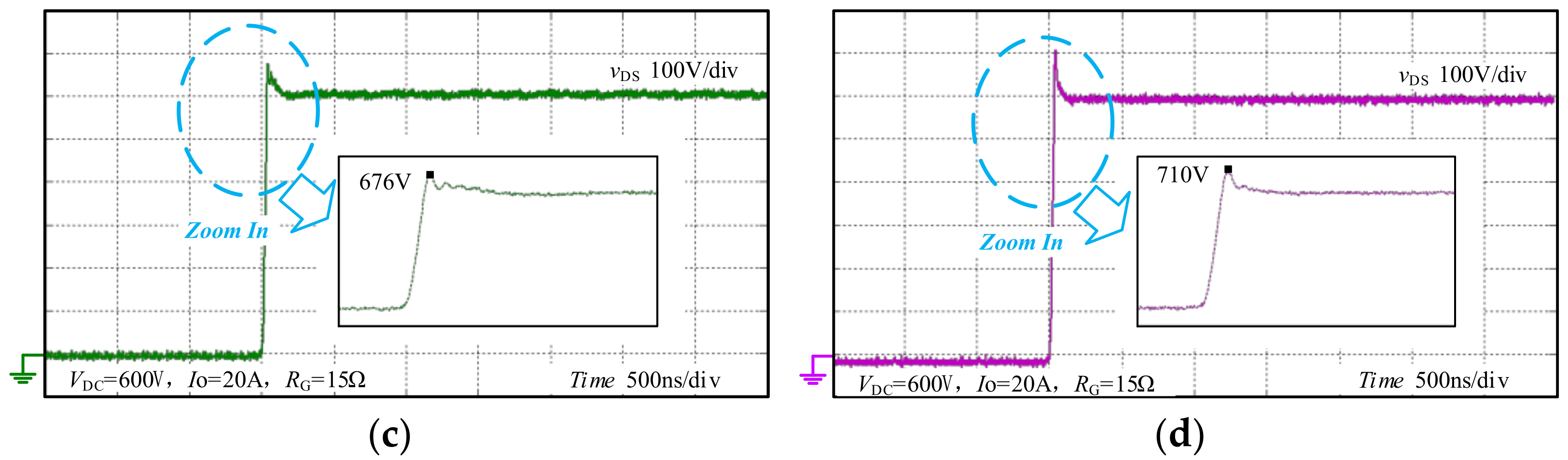
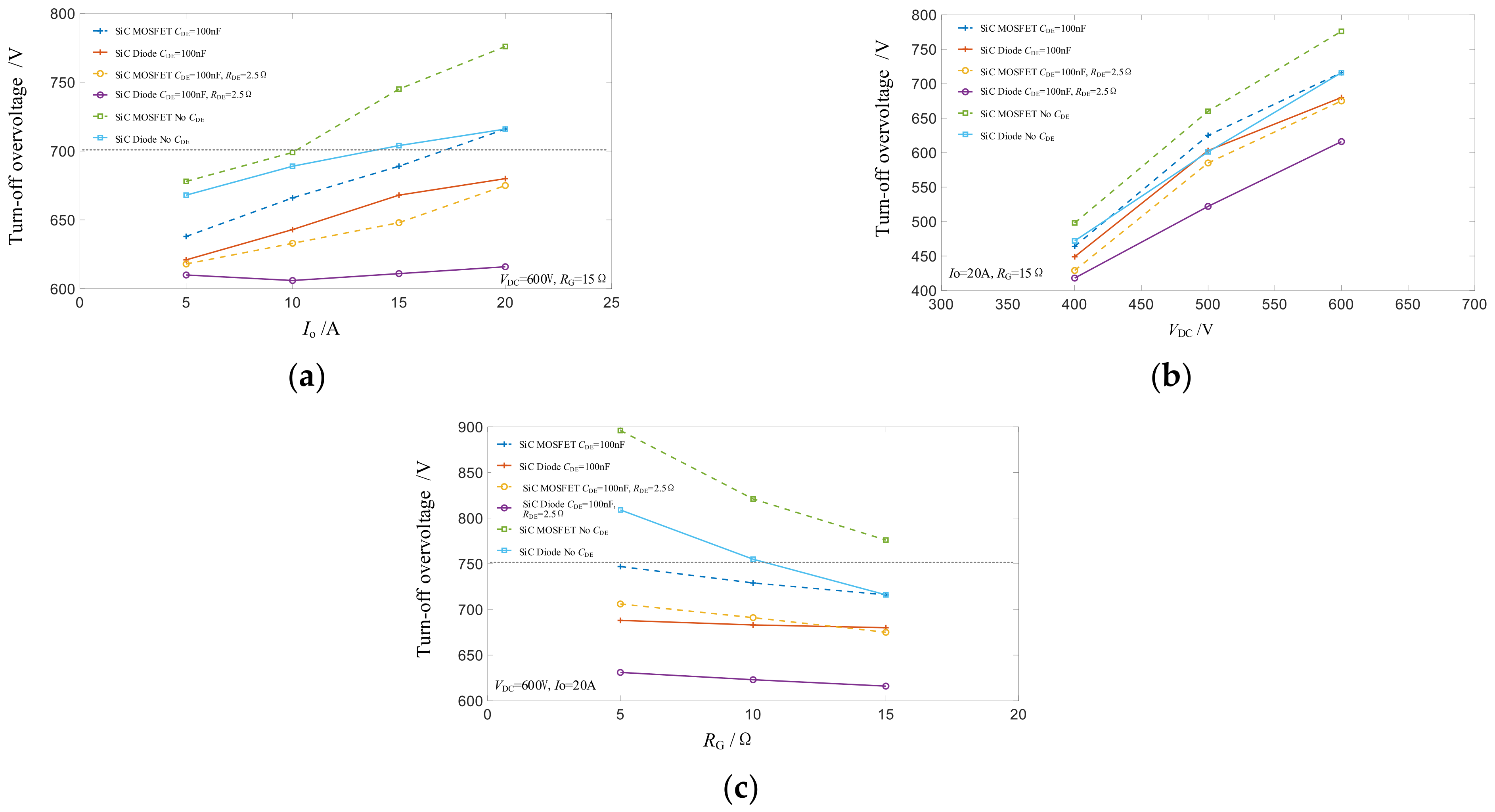
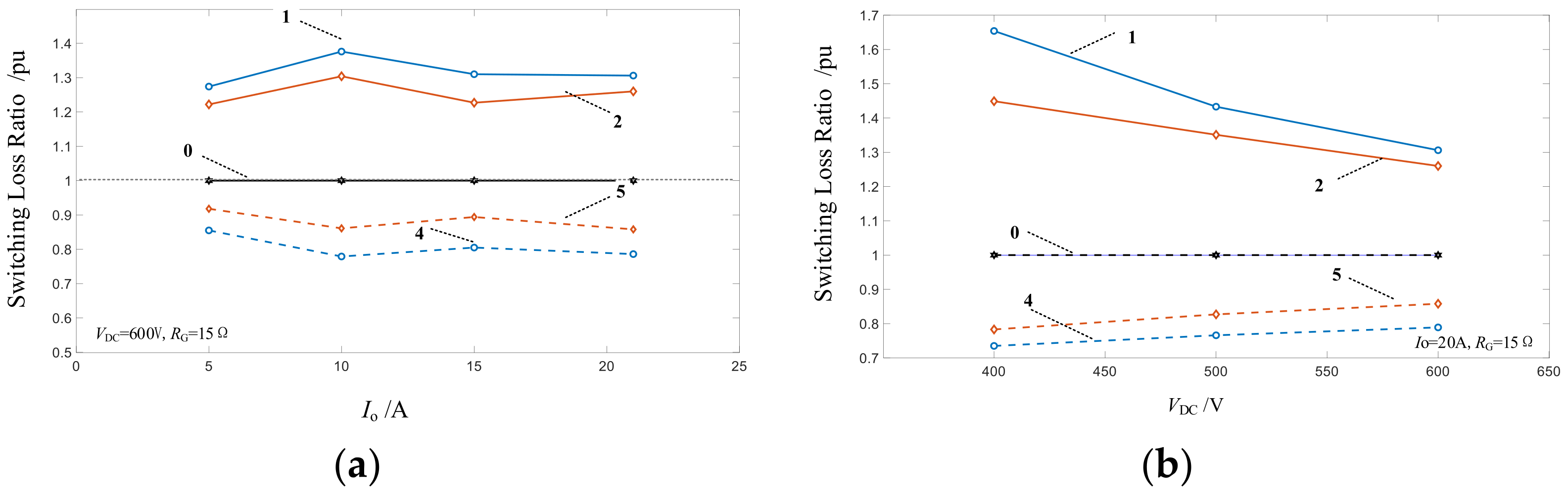
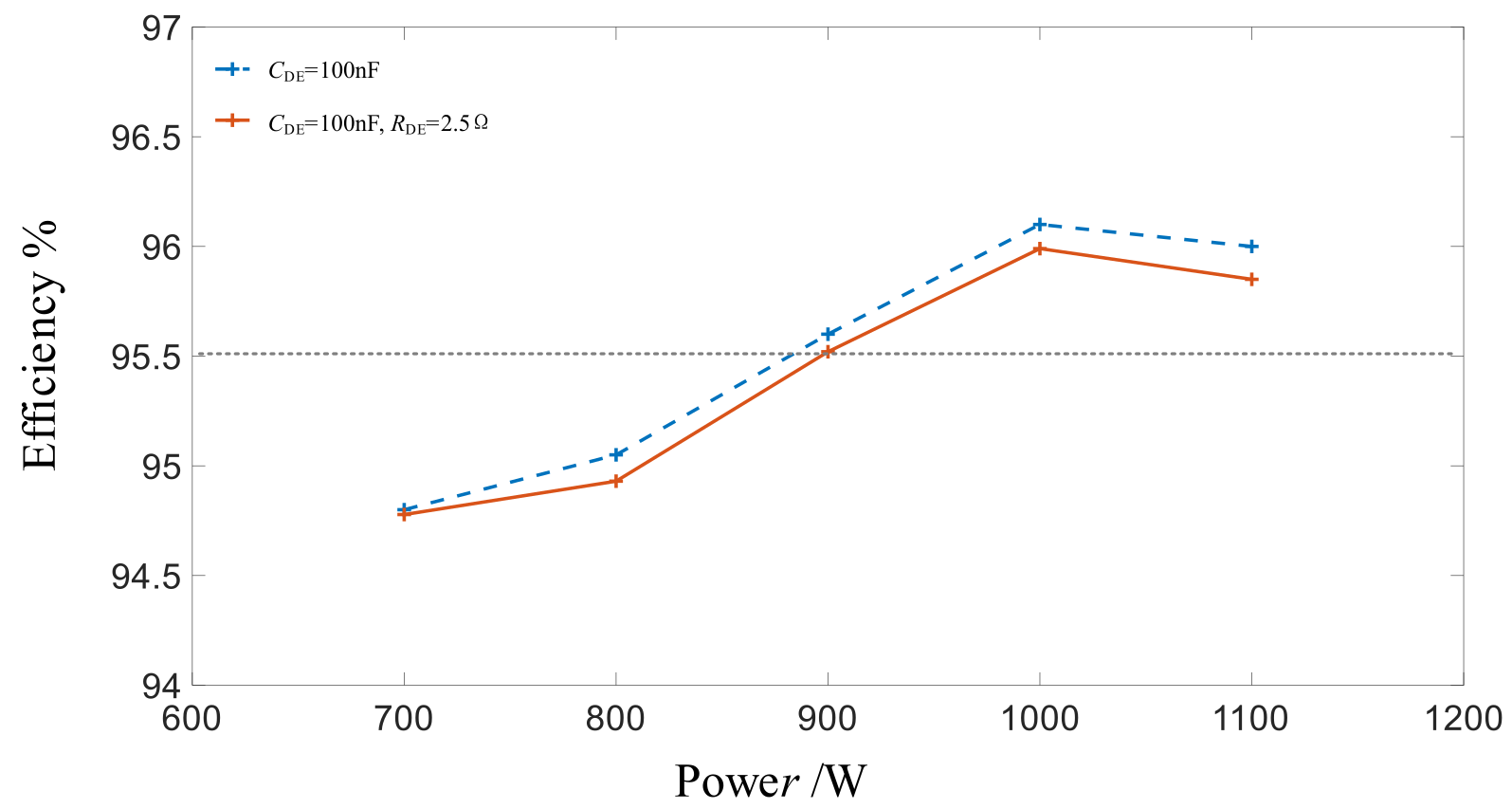
4. Experimental Results

To verify the suppressing effectiveness of DC-side snubbers, experiments using the 1200V SiC MOSFET C2M0080120D and the SiC diode C4D20120A by Cree Inc. are marked based on the double-pulse-test circuit. Figure 9 presents the testing platform, and Table 2 shows the test equipment used in the platform.
Figure 10 shows the experimental waveforms without and with capacitor CDE, in which capacitor CDE is the multilayer ceramic capacitor and CDE = 100 nF. In Figure 10a,b, the turn-off voltage of the SiC diode is presented. In Figure 10c,d, the turn-off voltage of the SiC MOSFET is presented. Compared to results in Figure 10a,c, without capacitor CDE, the turn-off overvoltage of the SiC diode and SiC MOSFET reduces obviously in Figure 10b,d. However, it is shown that the low-frequency oscillation overlays the high-frequency oscillation on the turn-off voltage of the SiC diode and SiC MOSFET.
Figure 11 shows the experimental waveforms with capacitor CDE and resistor RDE, in which CDE = 100 nF and RDE = 2.5 Ω or RDE = 5 Ω. In Figure 11a,b, the turn-off voltage of the SiC diode is presented. In Figure 11c,d, the turn-off voltage of the SiC MOSFET is presented. Compared to the results in Figure 10b,d, the low-frequency oscillations on the turn-off voltage of the SiC diode and SiC MOSFET are suppressed effectively. In addition, the turn-off overvoltage of the SiC diode and SiC MOSFET are reduced in Figure 11a,c, in which resistor RDE = 2.5 Ω. Comparing Figure 11a,c with Figure 11b,d, the turn-off overvoltage of the SiC diode and SiC MOSFET were obviously increased when RDE = 5 Ω.
Figure 12 presents the turn-off overvoltage of the SiC diode and the SiC MOSFET at different Io, VDC, and RG. From Figure 12, although the higher Io, higher VDC, and lower RG make the turn-off overvoltage higher, DC-side snubbers have effective suppression on the turn-off overvoltage of the SiC diode and SiC MOSFET. Moreover, the DC-side snubber with the damping resistor CDE-RDE is the most effective. Figure 13 presents the effect of DC-side snubbers on the switching losses of the SiC MOSFET at different Io and VDC. Figure 13 employs the switching losses of the SiC MOSFET without the snubber as a reference quantity and transforms the switching losses with DC-side snubbers into per-unit. The turn-on loss of the SiC MOSFET with DC-side snubbers increases, and the turn-off loss of the SiC MOSFET decrease, because a portion of parasitic inductors is decoupled from the power switching loop. Figure 14 presents the efficiency of a 1.1kW buck converter with DC-side snubbers. The tested conditions of the buck converter are presented in Table 3, and the efficiency is tested under open-loop control. From Figure 14, it is observed that the efficiency of the buck converter with CDE = 100 nF, RDE = 2.5 Ω is a little lower than with CDE = 100 nF, which is owning to the loss of RDE.

5. Conclusions

This paper designs effective DC-side snubbers to suppress the turn-off overvoltage and oscillation for SiC devices application. By the turn-off terminal impedances of the SiC diode and SiC MOSFET, the suppressing mechanisms and design principles of DC-side snubbers are investigated. Based on the above analysis and experimental results, the following conclusions can be drawn:
(1)
According to the guideline design for DC-side snubbers, the turn-off overvoltage and oscillation of the SiC diode and the SiC MOSFET can be suppressed effectively.
(2)
Capacitor CDE is closer to devices, which represents the parasitic inductors in the switching power loop are lower, which means the lower the peak impedance is and the lower the turn-off overvoltage is.
(3)
The DC-side snubber with the damping resistor CDE-RDE can not only eliminate the low-frequency oscillation on the turn-off voltage but also can reduce the turn-off overvoltage.

Author Contributions

Conceptualization, M.L.; methodology, M.L.; validation, M.L.; writing, M.L.; funding acquisition, J.C. and P.J. All authors have read and agreed to the published version of the manuscript.

Funding

This research was funded by the National Key R&D Program of China, grant number 2021YFF0700102 and the National Natural Science Foundation of China, grant number 51907002.

Data Availability Statement

Not applicable.

Conflicts of Interest

The authors declare no conflict of interest. The funders had no role in the design of the study; in the collection, analyses, or interpretation of data; in the writing of the manuscript; or in the decision to publish the results.

Appendix A

In Equation (1), Nd_1(s) and Dd_1(s) are as the following,
N d _ 1 s = C D E L b u s L P s 3 + C D E L b u s R D S _ o n s 2 + L P s + R D S _ o n
D d _ 1 s = C D E C F L b u s L P s 4 + C D E C F L b u s R D S _ o n s 3 + C D E L b u s + C F L P s 2 + C F R D S _ o n s + 1
In Equation (4), Nm2_1(s) and Dm2_1(s) are as the following,
N m 2 _ 1 s = s C D E C G D L b u s L P R G s 3 + C D E L b u s L P s 2 + C G D R G L P s + L P
D m 2 _ 1 s = C D E C D S C G D L b u s L P R G s 5 + C D E C o s s L b u s L P s 4 + C G D R G C D E L b u s + C D S L P s 3 + C D E L b u s + C o s s L P s 2 + C G D R G s + 1
In Equation (25), Nd_2(s) and Dd_2(s) are as the following,
N d _ 2 s = C D E L b u s L P s 3 + C D E L b u s R D E + C D E L b u s R D S _ o n + C D E L P R D E s 2 + L P + C D E R D E R D S _ o n s + R D S _ o n
D d _ 2 s = C D E C F L b u s L P s 4 + C D E C F L b u s R D S _ o n + C D E C F L P R D E s 3 + C D E L b u s + C F L P + C D E C F R D E R D S _ o n s 2 + C D E R D E + C F R D S _ o n s + 1
In Equation (26), Nm2_2(s) and Dm2_2(s) are as the following,
N m 2 _ 2 s = C D E C G D L b u s L P R G s 4 + C D E L b u s L P + C D E C G D L P R D E R G s 3 + C D E L b u s R D E + C G D L b u s R G + C D E L P R D E + C G D L P R G s 2 + L P s
D m 2 _ 2 s = C D E C D S C G D L b u s L P R G s 5 + C D E C o s s L b u s L P + C D E C D S C G D L P R D E R G s 4 + C G D C o s s L b u s R G + C D E C o s s L P R D E + C D S C G D L P R G s 3 + C D E L b u s + C o s s L P + C D E C G D R D E R G s 2 + C D E R D E + C G D R G s + 1

References

  1. Millan, J.; Godignon, P.; Perpiñà, X.; Pérez-Tomás, A.; Rebollo, J. A survey of wide bandgap power semiconductor devices. IEEE Trans. Power Electron. 2013, 29, 2155–2163. [Google Scholar] [CrossRef]
  2. Jouha, W.; Oualkadi, A.; Dherbécourt, P.; Joubert, E.; Masmoudi, M. Silicon carbide power MOSFET model: An accurate parameter extraction method based on the levenberg–marquardt algorithm. IEEE Trans. Power Electron. 2018, 33, 9130–9133. [Google Scholar] [CrossRef]
  3. Hashimoto, K.; Okuda, T.; Hikihara, T. A flyback converter with SiC power MOSFET operating at 10 MHz: Reducing leakage inductance for improvement of switching behaviors. In Proceedings of the 2018 International Power Electronics Conference (IPEC-Niigata 2018–ECCE Asia), Niigata, Japan, 20–24 May 2018; pp. 3757–3761. [Google Scholar]
  4. Zhang, W.; Zhang, Z.; Wang, F.; Costinett, D.L.; Tolbert, M.; Blalock, B.J. Characterization and Modeling of a SiC MOSFET′s turn-on overvoltage. In Proceedings of the 2018 IEEE Energy Conversion Congress and Exposition (ECCE), Portland, OR, USA, 23–27 September 2018; pp. 7003–7009. [Google Scholar]
  5. Koiwa, K.; Itoh, J.I. A maximum power density design method for nine switches matrix converter using SiC-MOSFET. IEEE Trans. Power Electron. 2015, 31, 1189–1202. [Google Scholar] [CrossRef]
  6. Hazra, S.; De, A.; Cheng, L.; Palmour, J.; Schupbach, M.; Hull, B.A.; Allen, S.; Bhattacharya, S. High switching performance of 1700-V, 50-A SiC power MOSFET over Si IGBT/BiMOSFET for advanced power conversion applications. IEEE Trans. Power Electron. 2015, 31, 4742–4754. [Google Scholar]
  7. Lemmon, A.; Mazzola, M.; Gaord, J.; Parker, C. Stability considerations for silicon carbide field-effect transistors. IEEE Trans. Power Electron. 2013, 28, 4453–4459. [Google Scholar] [CrossRef]
  8. Mohan, N.; Undeland, T.M. Power Electronics: Converters, Applications, and Design; John Wiley & Sons: Hoboken, NJ, USA, 2007. [Google Scholar]
  9. Zhang, Z.; Guo, B.; Wang, F.; Tolbert, L.M.; Blalock, B.J.; Liang, Z. Impact of ringing on switching losses of wide band-gap devices in a phase-leg configuration. In Proceedings of the 2014 IEEE Applied Power Electronics Conference and Exposition—APEC 2014, Fort Worth, TX, USA, 16–20 March 2014; pp. 2542–2549. [Google Scholar]
  10. Kadavelugu, A.; Baek, S.; Dutta, S.; Bhattacharya, S.; Scofield, J. High-frequency design considerations of dual active bridge 1200 V SiC MOSFET DC-DC converter. In Proceedings of the 2011 Twenty-Sixth Annual IEEE Applied Power Electronics Conference and Exposition (APEC), Fort Worth, TX, USA, 6–11 March 2011; pp. 314–320. [Google Scholar]
  11. Wang, Y.; De Haan, S.W.H.; Ferreira, J.A. Potential of improving PWM converter power density with advanced components. In Proceedings of the 2009 13th European Conference on Power Electronics and Applications, Barcelona, Spain, 8–10 September 2009; pp. 1–10. [Google Scholar]
  12. Liu, Q.; Wang, S.; Baisden, A.C.; Wang, F.; Boroyevich, D. EMI suppression in voltage source converters by utilizing dc-link decoupling capacitors. IEEE Trans. Power Electron. 2007, 22, 1417–1428. [Google Scholar]
  13. Chen, Z. Electrical Integration of SiC Power Devices for High-Power-Density Applications; Virginia Polytechnic Institute and State University: Blacksburg, VA, USA, 2013. [Google Scholar]
  14. Chen, Z.; Yao, Y.; Boroyevich, D.; Ngo, K.; Mattavelli, P. Exploration of a switching loop snubber for parasitic ringing suppression. In Proceedings of the 2014 IEEE Energy Conversion Congress and Exposition (ECCE), Pittsburgh, PA, USA, 14–18 September 2014; pp. 1605–1612. [Google Scholar]
  15. Zhang, Z.; Wang, F. Driving and Characterization of wide bandgap semiconductors for voltage source converter applications. In Proceedings of the 2014 IEEE Wide Bandgap Power Devices and Applications, Knoxville, TN, USA, 13–15 October 2014; pp. 1–84. [Google Scholar]
  16. Witcher, J.B. Methodology for Switching Characterization of Power Devices and Modules; Virginia Polytechnic Institute and State University: Blacksburg, VA, USA, 2003. [Google Scholar]
  17. Pilli, N.K.; Singh, S.K. Influence of peak gate current and rate of rise of gate current on switching behaviour of SiC MOSFET. In Proceedings of the 2017 IEEE Transportation Electrification Conference (ITEC-India), Pune, India, 13–15 December 2017; pp. 1–6. [Google Scholar]
  18. Joko, M.; Goto, A.; Hasegawa, M.; Miyahara, S.; Murakami, H. Snubber circuit to suppress the voltage ringing for SiC device. In Proceedings of the PCIM Europe 2015, Nuremberg, Germany, 19–20 May 2015; pp. 1–6. [Google Scholar]
  19. Liu, T.; Ning, R.; Wong, T.T.; Shen, Z.J. Modeling and Analysis of SiC MOSFET Switching Oscillations. IEEE J. Emerg. Sel. Top. Power Electron. 2016, 4, 747–756. [Google Scholar] [CrossRef]
  20. Yamashita, Y.; Furuta, J.; Inamori, S.; Kobayashi, K. Design of RCD snubber considering wiring inductance for MHz-switching of SiC-MOSFET. In Proceedings of the 2017 IEEE 18th Workshop on Control and Modeling for Power Electronics (COMPEL), Stanford, CA, USA, 9–12 July 2017; pp. 1–6. [Google Scholar]
  21. Wang, J.; Li, R.T.; Chung, H.S. An Investigation into the Effects of the Gate Drive Resistance on the Losses of the MOSFET–Snubber–Diode Configuration. IEEE Trans. Power Electron. 2012, 27, 2657–2672. [Google Scholar] [CrossRef]
  22. Li, H.; Munk-Nielsen, S. Challenges in switching SiC MOSFET without ringing. In Proceedings of the PCIM Europe 2014, Nuremberg, Germany, 20–22 May 2014; pp. 1–6. [Google Scholar]
  23. Chen, Z.; Boroyevich, D.; Mattavelli, P.; Ngo, K. A frequency-domain study on the effect of DC-link decoupling capacitors. In Proceedings of the 2018 IEEE Energy Conversion Congress and Exposition (ECCE), Denver, CO, USA, 28 October 2013; pp. 1886–1893. [Google Scholar]
  24. Petterteig, A.; Lode, J.; Undeland, T.M. IGBT turn-off losses for hard switching and with capacitive snubbers. In Proceedings of the 1991 IEEE Industry Applications Society Annual Meeting, Dearborn, MI, USA, 28 September–4 October 1991; pp. 1501–1507. [Google Scholar]
  25. Liang, M.; Li, Y.; Chen, Q.; Lu, Y.; Yu, H.; Zheng, T.Q.; Guo, H.; Zhao, F. Research on an improved DC-side snubber for suppressing the turn-off overvoltage and oscillation in high speed SiC MOSFET application. In Proceedings of the 2014 IEEE Energy Conversion Congress and Exposition (ECCE), Cincinnati, OH, USA, 1–5 October 2017; pp. 1358–1365. [Google Scholar]
  26. Liang, M.; Zheng, T.Q.; Li, Y. An Improved Analytical Model for Predicting the Switching Performance of SiC MOSFETs. J. Power Electron. 2016, 16, 374–387. [Google Scholar] [CrossRef] [Green Version]
Figure 1. Phase-leg configuration with DC-side Snubber CDE.
Electronics 11 03874 g001
Figure 2. Switching waveforms during the turn-on and turn-off transitions of the SiC MOSFET.
Electronics 11 03874 g002
Figure 3. Equivalent circuit with capacitor CDE (a) at Stage 4 and (b) at Stage 7 and Stage 8.
Electronics 11 03874 g003
Figure 4. Amplitude–frequency curves of the terminal impedances, Zd_1 and Zm2_1, with different CDE (a) at Stage 4 and (b) at Stage 7 and Stage 8.
Electronics 11 03874 g004
Figure 5. Amplitude–frequency curves of terminal impedances, Zd_1 and Zm2_1, with different n values (a) at Stage 4 and (b) at Stage 7 and Stage 8.
Electronics 11 03874 g005
Figure 6. Equivalent circuits with capacitor CDE and resistor RDE (a) at Stage 4, (b) at Stage 7 and Stage 8.
Electronics 11 03874 g006
Figure 7. Range of resistor RDE with different n.
Electronics 11 03874 g007
Figure 8. Amplitude–frequency curves of the terminal impedances, Zd_2 and Zm2_2, with capacitor CDE and resistor RDE (a) at Stage 4 and (b) at Stage 7 and Stage 8.
Electronics 11 03874 g008
Figure 9. DC-side snubber testing platform.
Electronics 11 03874 g009
Figure 10. Tested waveforms without and with capacitor CDE. (a) Turn-off voltage of the SiC diode without CDE, (b) turn-off voltage of the SiC diode with CDE = 100 nF, (c) turn-off voltage of the SiC MOSFET without CDE, and (d) turn-off voltage of the SiC MOSFET with CDE = 100 nF.
Electronics 11 03874 g010
Figure 11. Tested waveforms with capacitor CDE and resistor RDE. (a) Turn-off voltage of the SiC diode at CDE = 100 nF and RDE = 2.5 Ω, (b) turn-off voltage of the SiC diode at CDE = 100 nF and RDE = 5 Ω, (c) turn-off voltage of the SiC MOSFET at CDE = 100 nF and RDE = 2.5 Ω, and (d) turn-off voltage of the SiC MOSFET at CDE = 100 nF and RDE = 5 Ω.
Electronics 11 03874 g011aElectronics 11 03874 g011b
Figure 12. Turn-off overvoltage of the SiC diode and the SiC MOSFET with DC-side snubbers (a) at different Io, (b) at different VDC, and (c) at different RG.
Electronics 11 03874 g012
Figure 13. Switching losses of the SiC MOSFET with DC-side snubbers (a) at different Io and (b) at different VDC. (Note: 0: turn-on loss or turn-off loss with no CDE, 1: turn-on loss with CDE = 100 nF, 2: turn-on loss with CDE = 100 nF and RDE = 2.5 Ω, 4: turn-off loss with CDE = 100 nF, 5: turn-off loss with CDE = 100 nF and RDE = 2.5 Ω).
Electronics 11 03874 g013
Figure 14. Efficiency of the buck converter with DC-side snubbers.
Electronics 11 03874 g014
Table 1. Parameters for drawing the amplitude–frequency curve.
ParameterValueParameterValue
RDS_on0.2 ΩLP50 nH
CGD7.6 pFLbus150 nH
CDS75 pFRG15 Ω
CF67 pF
Table 2. Test equipment used in the platform.
ModelTypeBandwidth
Tektronix TCP0030ACurrent probe120 M
Tektronix DPO4054BOscilloscope500 M
CP3308RPassive probe300 M
SSDN-10Coaxial Shunt2000 M
Table 3. Efficiency-tested conditions of the buck converter.
ParameterValueParameterValue
Input voltage600 VSwitching frequency50 kHz
Output voltage150 VOutput inductor100 µH
Output power700 W~1100 WOutput capacitor220 µF
Publisher′s Note: MDPI stays neutral with regard to jurisdictional claims in published maps and institutional affiliations.

