
A New Gate Driver for Suppressing Crosstalk of SiC MOSFET

Abstract
:1. Introduction
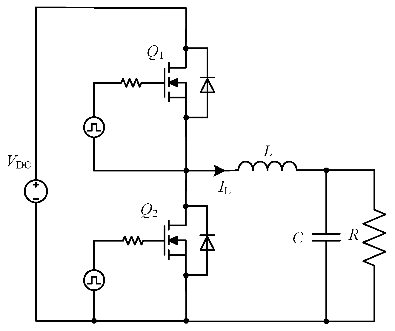
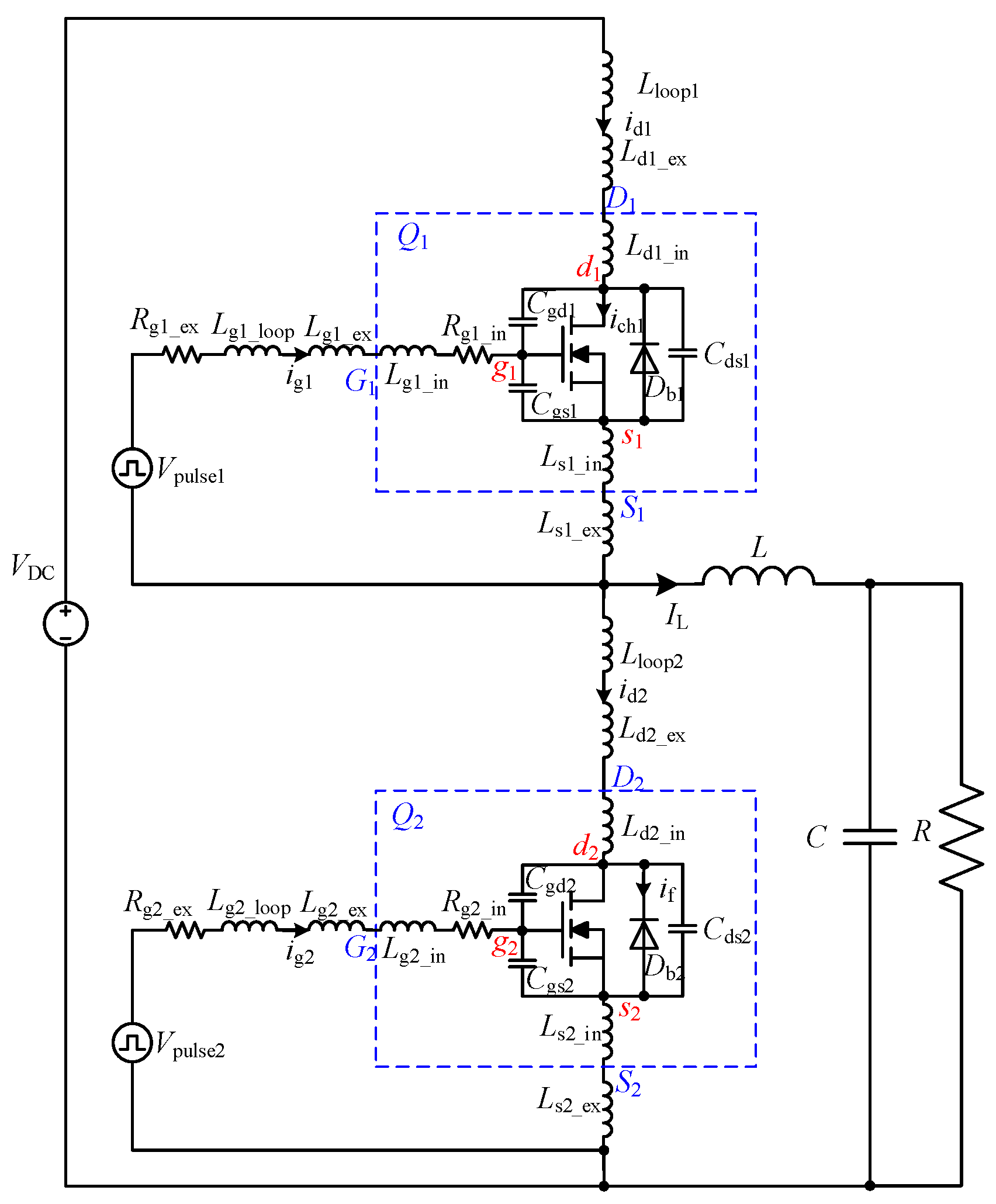
2. Crosstalk Mechanisms of SiC MOSFET
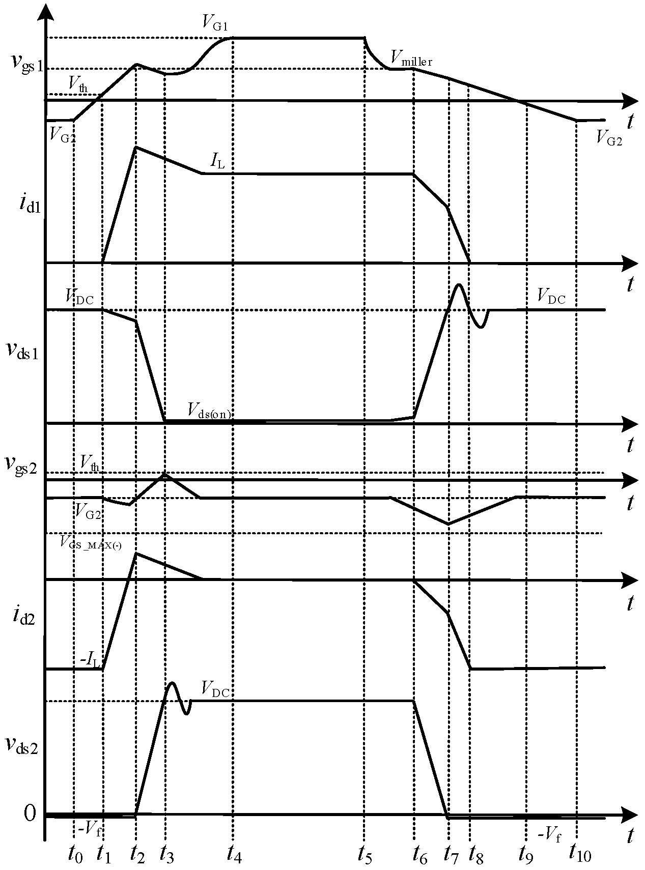
2.1. Crosstalk Issue during Q1 Turn-ON Transition
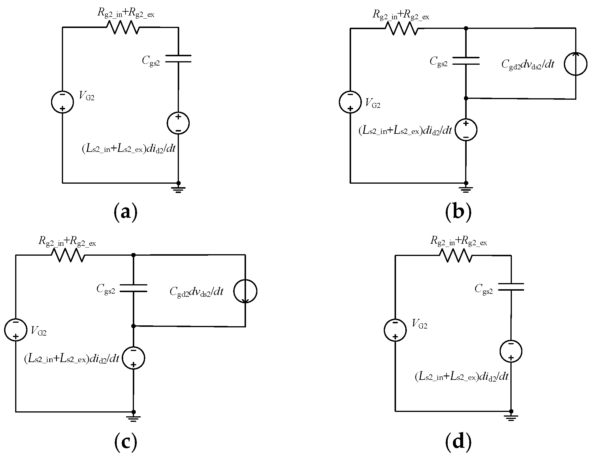
2.2. Crosstalk Issue during Q1 Turn-OFF Transition
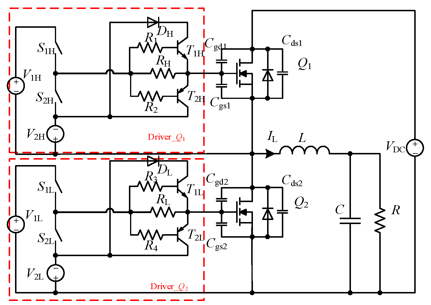
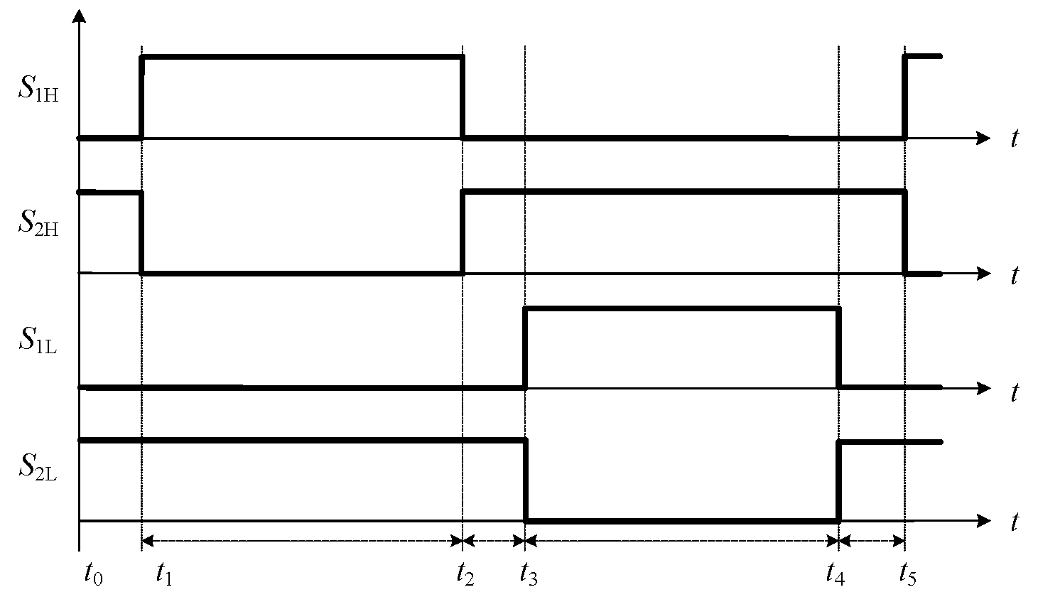
3. A New Gate Driver for Suppressing Crosstalk Issue of SiC MOSFET
3.1. Operating Principle
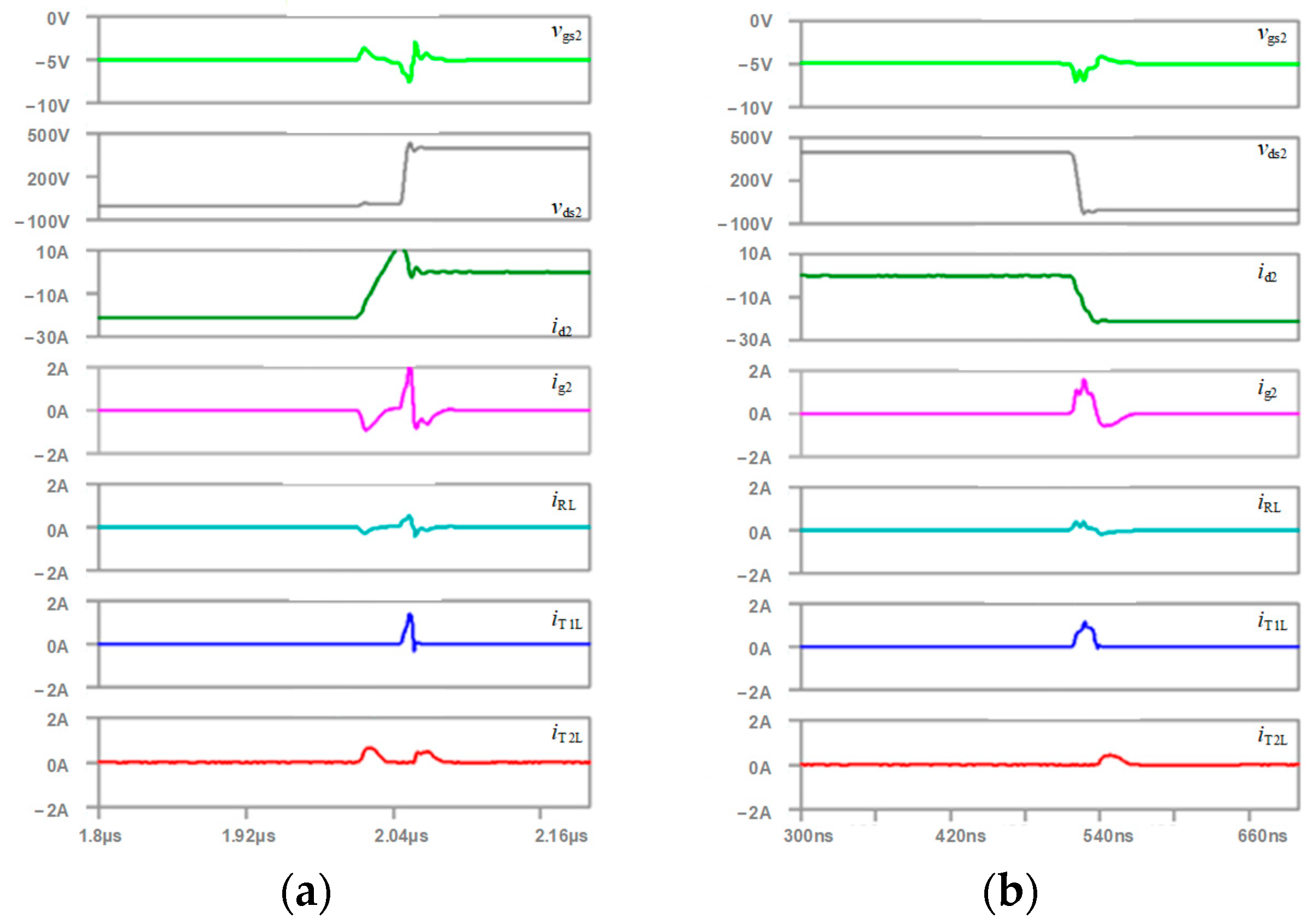
3.2. Simulation Results
3.3. Comparisons
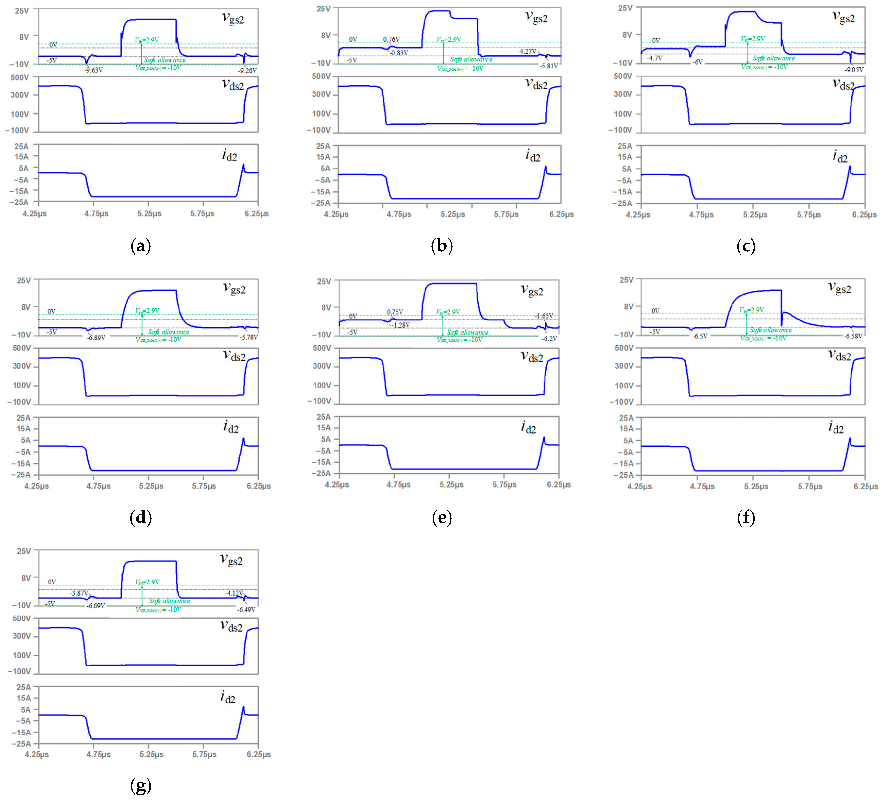
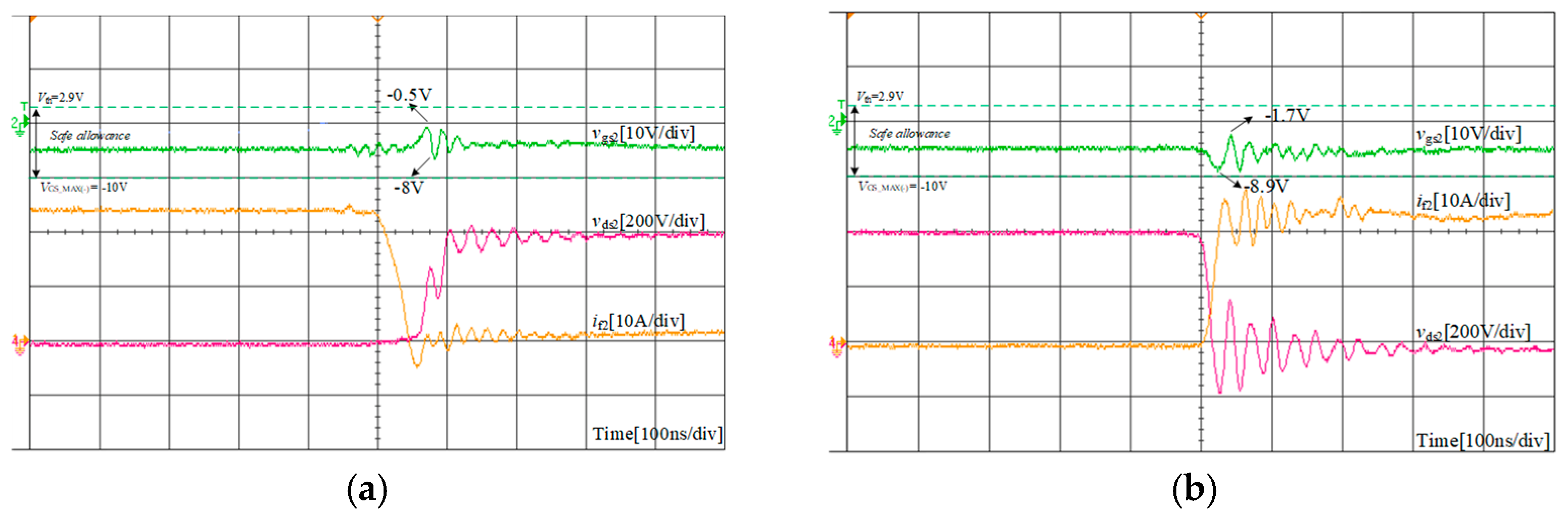
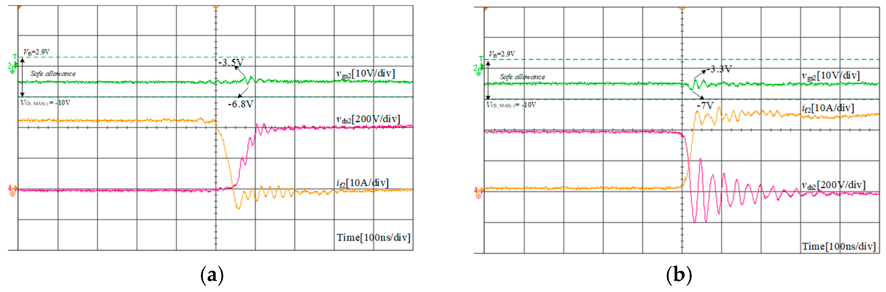
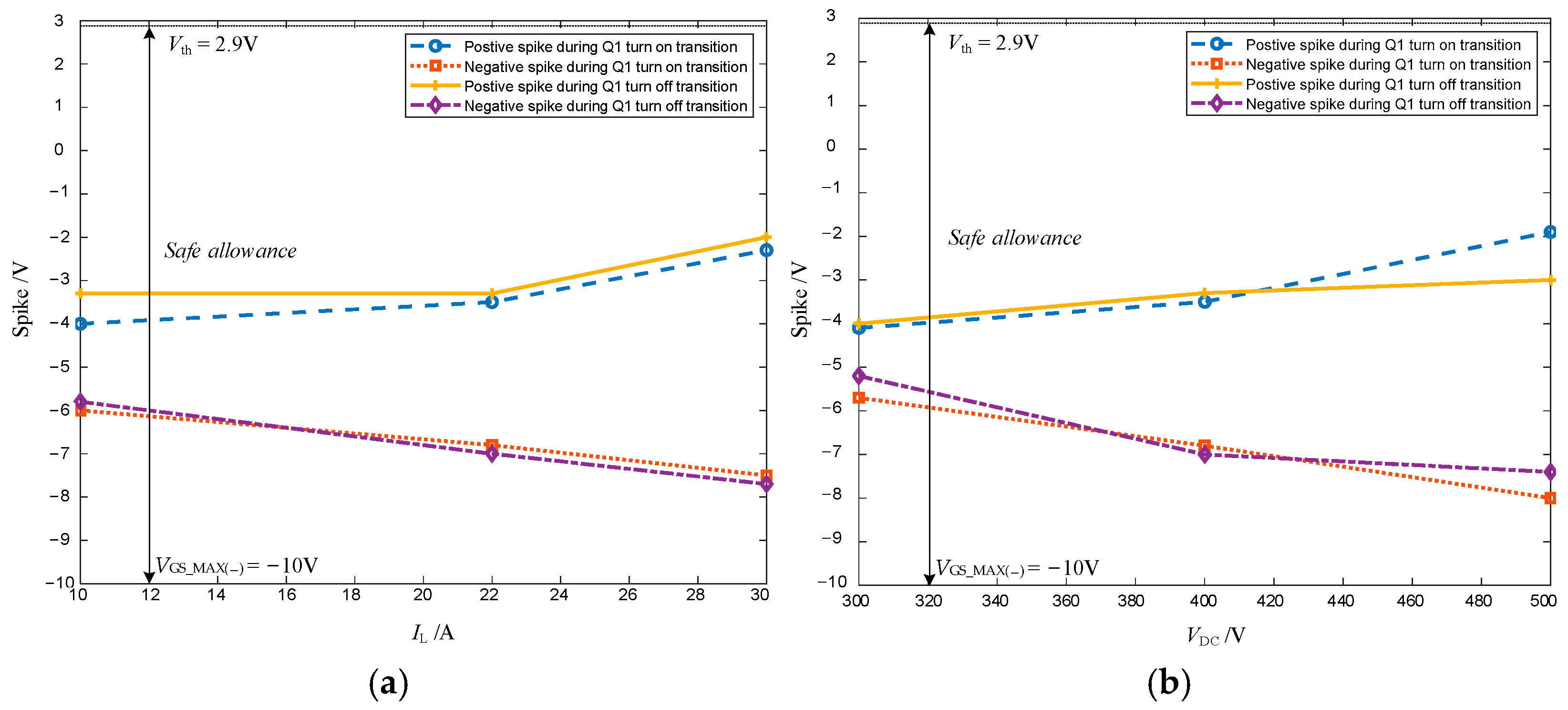
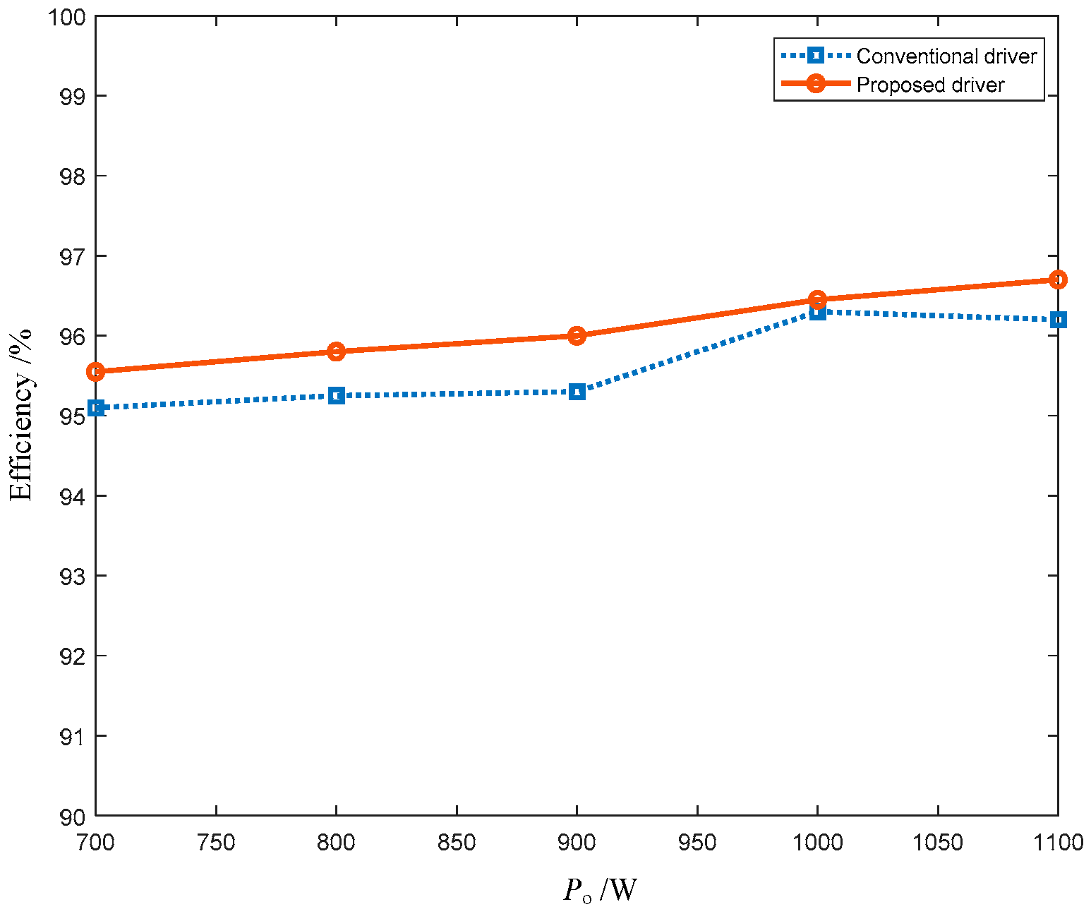
4. Verification
5. Conclusions
Author Contributions
Funding
Data Availability Statement
Conflicts of Interest
References
- Zhang, L.; Zheng, Z.; Lou, X. A review of WBG and Si devices hybrid applications. Chin. J. Electr. Eng. 2021, 7, 1–20. [Google Scholar] [CrossRef]
- Narasipuram, R.P.; Mopidevi, S. A technological overview & design considerations for developing electric vehicle charging stations. J. Energy Storage 2021, 43, 103225. [Google Scholar]
- Oliveira, J.; Alhoussen, A.; Loiselay, F.; Morel, H.; Planson, D. Switching Behavior and Comparison of Wide Bandgap Devices for Automotive Applications. In Proceedings of the 2021 23rd European Conference on Power Electronics and Applications (EPE’21 ECCE Europe), Ghent, Belgium, 6–10 September 2021; pp. 1–10. [Google Scholar]
- Shah, S.S.; Narwal, R.; Bhattacharya, S.; Kanale, A.; Cheng, T.H.; Mehrotra, U.; Agarwal, A.; Baliga, B.J.; Hopkins, D.C. Optimized AC/DC Dual Active Bridge Converter using Monolithic SiC Bidirectional FET (BiDFET) for Solar PV Applications. In Proceedings of the 2021 IEEE Energy Conversion Congress and Exposition (ECCE), Vancouver, BC, Canada, 10–14 October 2021; pp. 568–575. [Google Scholar]
- Iannaccone, G.; Sbrana, C.; Morelli, I.; Strangio, S. Power Electronics Based on Wide-Bandgap Semiconductors: Opportunities and Challenges. IEEE Access 2021, 9, 139446–139456. [Google Scholar] [CrossRef]
- Xu, Y.; Yuan, X.; Ye, F.; Wang, Z.; Zhang, Y.; Diab, M.; Zhou, W. Impact of High Switching Speed and High Switching Frequency of Wide-Bandgap Motor Drives on Electric Machines. IEEE Access 2021, 9, 82866–82880. [Google Scholar] [CrossRef]
- Yu, S.; Wang, J.; Zhang, X.; Liu, Y.; Jiang, N.; Wang, W. The potential impact of using traction inverters with SiC MOSFETs for electric buses. IEEE Access 2021, 9, 51561–51572. [Google Scholar] [CrossRef]
- Zhang, C.; Srdic, S.; Lukic, S.; YKang Choi, E.; Tafti, E. A SiCbased 100 kW high-power-density (34 kW/L) electric vehicle traction inverter. In Proceedings of the 2018 IEEE Energy Conversion Congress and Exposition (ECCE), Portland, OR, USA, 23–27 September 2018. [Google Scholar]
- Nguyen, H.V.; Lee, D.C.; Blaabjerg, F. A novel SiC-based multifunctional onboard battery charger for plug-in electric vehicles. IEEE Trans. Power Electron. 2021, 36, 5635–5646. [Google Scholar] [CrossRef]
- Abbasi, M.; Emamalipour, R.; Cheema, M.A.M.; Lam, J. A new fully magnetically coupled SiC-based DC/DC step-up LLC resonant converter with inherent balanced voltage sharing for renewable energy systems with a medium voltage DC grid. In Proceedings of the 2019 IEEE Energy Conversion Congress and Exposition (ECCE), Baltimore, MD, USA, 29 September–3 October 2019; pp. 5542–5547. [Google Scholar]
- Schwarzer, G.U.; Buschhorn, S.; Vogel, K. System benefits for solar inverters using SiC semiconductor modules. In Proceedings of the International Exhibition and Conference for Power Electronics, Intelligent Motion, Renewable Energy and Energy Management, Nuremberg, Germany, 20–22 May 2014; pp. 787–794. [Google Scholar]
- She, X.; Huang, A.Q.; Lucía, Ó.; Ozpineci, B. Review of silicon carbide power devices and their applications. IEEE Trans. Ind. Electron. 2017, 64, 8193–8205. [Google Scholar] [CrossRef]
- Lemmon, A.; Mazzola, M.; Gaord, J.; Parker, C. Stability considerations for silicon carbide field-effect transistors. IEEE Trans. Power Electron. 2013, 28, 4453–4459. [Google Scholar] [CrossRef]
- Mohan, N.; Undeland, T.M. Power Electronics: Converters, Applications, and Design; John Wiley & Sons: Hoboken, NJ, USA, 2007. [Google Scholar]
- Zhang, Z.; Guo, B.; Wang, F.; Tolbert, L.M.; Blalock, B.J.; Liang, Z. Impact of ringing on switching losses of wide band-gap devices in a phase-leg configuration. In Proceedings of the 2014 IEEE Applied Power Electronics Conference and Exposition—APEC, Fort Worth, TX, USA, 16–20 March 2014; pp. 2542–2549. [Google Scholar]
- Jahdi, S.; Alatise, O.; Gonzalez, J.A.; Bonyadi, R.; Ran, L.; Mawby, P. Temperature and switching rate dependence of crosstalk in Si-IGBT and SiC power modules. IEEE Trans. Ind. Electron. 2015, 63, 849–863. [Google Scholar] [CrossRef] [Green Version]
- Nishigaki, A.; Umegami, H.; Hattori, F.; Martinez, W.; Yamamoto, M. An analysis of false turn-on mechanism on power devices. In Proceedings of the 2014 IEEE Energy Conversion Congress and Exposition (ECCE), Pittsburgh, PA, USA, 14–18 September 2014; pp. 2988–2993. [Google Scholar]
- Wang, J.; Chung, H.S. Impact of parasitic elements on the spurious pulse in synchronous buck converter. IEEE Trans. Power Electron. 2014, 29, 6672–6685. [Google Scholar] [CrossRef]
- Xu, S.; Liu, X.; Sun, W. Modelling of power metal-oxide semiconductor field-effect transistor for the analysis of switching characteristics in half-bridge converters. IET Circuits Devices Syst. 2010, 4, 327–336. [Google Scholar] [CrossRef]
- Xu, S.; Sun, W.; Sun, D. Analysis and design optimization of brushless DC motor’s driving circuit considering the Cdv/dt induced effect. In Proceedings of the 2010 IEEE Energy Conversion Congress and Exposition, Atlanta, GA, USA, 12–16 September 2010; pp. 2091–2095. [Google Scholar]
- Yang, B.; Zhang, J. Effect and utilization of common source inductance in synchronous rectification. In Proceedings of the 2005 IEEE Applied Power Electronics Conference and Exposition, Austin, TX, USA, 6–10 March 2005; pp. 1407–1411. [Google Scholar]
- Yin, S.; Tseng, K.J.; Tong, C.F.; Simanjorang, R.; Gajanayake, C.J.; Nawawi, A.; Liu, Y.; Liu, Y.; See, K.Y.; Sakanova, A.; et al. Gate driver optimization to mitigate shoot-through in high-speed switching SiC half bridge module. In Proceedings of the 2015 IEEE 11th International Conference on Power Electronics and Drive Systems, Sydney, NSW, Australia, 9–12 June 2015; pp. 484–491. [Google Scholar]
- Wang, J.; Chung, H.S. A novel RCD level shifter for elimination of spurious turn-on in the bridge-leg configuration. IEEE Trans. Power Electron. 2014, 30, 976–984. [Google Scholar] [CrossRef]
- Cree. SiC MOSFET Isolated Gate Driver. 2018. Available online: https://assets.wolfspeed.com/uploads/2020/12/CPWRAN21.pdf (accessed on 1 April 2018).
- Zhang, Z.; Wang, F.; Tolbert, L.M.; Blalock, B.J.; Costinett, D.J. Active gate driver for fast switching and cross-talk suppression of SiC devices in a phase-leg configuration. In Proceedings of the 2015 IEEE Applied Power Electronics Conference and Exposition (APEC), Charlotte, NC, USA, 15–19 March 2015; pp. 774–781. [Google Scholar]
- Wu, X.; Zaman, H.; Wu, P.; Jia, R.; Zhao, X.; Wu, X. A quasi-multilevel gate driver for fast switching and crosstalk suppression of SiC devices. IEEE Access 2020, 8, 191403–191412. [Google Scholar] [CrossRef]
- Zhang, Z.; Wang, F.; Tolbert, L.M.; Blalock, B.J. A gate assist circuit for cross talk suppression of SiC devices in a phase-leg configuration. In Proceedings of the 2013 IEEE Energy Conversion Congress and Exposition (ECCE), Denver, CO, USA, 15–19 September 2013; pp. 2536–2543. [Google Scholar]
- Zhou, Q.; Gao, F.; Jiang, T. A gate driver of SiC MOSFET with passive triggered auxiliary transistor in a phase-leg configuration. In Proceedings of the 2015 IEEE Energy Conversion Congress and Exposition (ECCE), Montreal, QC, Canada, 20–24 September 2015; pp. 7023–7030. [Google Scholar]
- Gao, F.; Zhou, Q.; Wang, P.; Zhang, C. A gate driver of SiC MOSFET for suppressing the negative voltage spikes in a bridge circuit. IEEE Trans. Power Electron. 2017, 33, 2339–2353. [Google Scholar] [CrossRef]
- Zhang, Z.; Wang, F.; Tolbert, L.M.; Blalock, B.J. Active gate driver for crosstalk suppression of SiC devices in a phase-leg configuration. IEEE Trans. Power Electron. 2013, 29, 1986–1997. [Google Scholar] [CrossRef]
- Li, Y.; Liang, M.; Chen, J.; Zheng, T.Q.; Guo, H. A low gate turn-off impedance driver for suppressing crosstalk of SiC MOSFET based on different discrete packages. IEEE J. Emerg. Sel. Top. Power Electron. 2018, 7, 353–365. [Google Scholar] [CrossRef]
- Texas Instruments. IGBT & SiC Gate Driver Fundamentals. 2019. Available online: https://www.ti.com/lit/eb/slyy169/slyy169.pdf (accessed on 1 July 2019).
- Texas Instruments. ISO5852S Datasheet. 2017. Available online: https://www.ti.com (accessed on 1 January 2017).
- BROADCOM. ACPL-337J-000E Datasheet. 2014. Available online: https://docs.broadcom.com/doc/AV02-4390EN (accessed on 9 May 2014).
- Analog Devices. ADUM4135BRWZ Datasheet. 2020. Available online: https://www.analog.com/media/en/technical-documentation/data-sheets/ADuM4135.pdf (accessed on 1 July 2015).
- Zhang, Z.; Wang, F.; Tolbert, L.M.; Blalock, B.J.; Costinett, D.J. Realization of high speed switching of SiC power devices in voltage source converters. In Proceedings of the 2015 IEEE 3rd Workshop on Wide Bandgap Power Devices and Applications (WiPDA), Blacksburg, VA, USA, 2–4 November 2015; pp. 28–33. [Google Scholar]
- Chen, J.; Li, Y.; Liang, M. A gate driver based on variable voltage and resistance for suppressing overcurrent and overvoltage of SiC MOSFETs. Energies 2019, 12, 1640. [Google Scholar] [CrossRef]


| Parameter | Value | Parameter | Value |
|---|---|---|---|
| Inner gate resistor (Rg_in) | 3.9 Ω | Threshold voltage (Vth) | 2.9 V |
| Gate inductors (Lg_in + Lg_ex) | 15 nH | Gate-source capacitor (Cgs) | 1122 pF |
| Common source inductors (Ls_in + Ls_ex) | 9 nH | Gate-drain capacitor (Cgd) | 8 pF |
| Drain inductors (Ld_in + Ld_ex) | 6 nH | Drain-source capacitor (Cds) | 92 pF |
| Maximum negative driver voltage (VGS_MAX(−)) | −10 V |
| Parameter | Value | Parameter | Value |
|---|---|---|---|
| Input voltage | 400 V | Power loop inductor | 25 nH |
| Output current | 21 A | Power loop inductor | 25 nH |
| Switching frequency | 500 kHz | Positive driver voltage (V1H and V1L) | 18 V |
| Width of the gate signal | 500 ns | Negative driver voltage (V2H and V2L) | −5 V |
| Dead time | 500 ns | Gate resistor (RH and RL) | 10 Ω |
| Gate loop inductor | 10 nH | Base resistor of BJT(R1~R4) | 1 Ω |
| Parameter | |
|---|---|
| Driver in [24] | V1L = 18 V, V2L = 5 V, RL = 10 Ω |
| Driver in [25] | V1L = 23 V, V2L = 5 V, RL = 10 Ω |
| Driver in [26] | V1L = 18 V, VZ = 4.7 V, RL_ON = 10 Ω, RL_OFF = 10 Ω, RC = 1 Ω, RM = 0.1 Ω, CZ = 100 nF |
| Driver in [27] | V1L = 18 V, V2L = 5 V, RL = 10 Ω |
| Driver in [30] | V1L = 18 V, V2L = 5 V, RL = 10 Ω, Ca = 5 nF |
| Driver in [31] | V1L = 18 V, V2L = 5 V, RL_ON = 10 Ω, RL_OFF = 10 Ω, Ca1 = 5 nF |
| Proposed driver | V1L = 18 V, V2L = 5 V, RL = 10 Ω |
| Suppression Method | Assistant Components | Implementation | Suppression Effectiveness | |
|---|---|---|---|---|
| Driver in [25] | Shift driver voltage and provide a low impedance path | One diode, two MOSFETs and drivers for MOSFETs | hard | Good |
| Driver in [26] | Shift driver voltage | One resistor, one MOSFET and driver for MOSFET | Medium | Bad |
| Driver in [27] | Shift driver voltage and provide a low impedance path | Two diodes, two switches (if MOSFETs, drivers are needed) | hard | Medium |
| Driver in [30] | provide a low impedance path | One capacitor, one MOSFET and driver for MOSFET | Medium | Good |
| Driver in [31] | provide a low impedance path | Two capacitors | Easy | Good |
| Proposed driver | provide a low impedance path | Two BJTs and one diode | Easy | Good |
| Parameter | Value | Parameter | Value |
|---|---|---|---|
| Input voltage | 400 V | Dead time | 500 ns |
| Output voltage | 100 V | Output inductor | 100 µH |
| Output power | 700~1100 W | Output capacitor | 220 µF |
| Switching frequency | 50 kHz |
Publisher’s Note: MDPI stays neutral with regard to jurisdictional claims in published maps and institutional affiliations. |
© 2022 by the authors. Licensee MDPI, Basel, Switzerland. This article is an open access article distributed under the terms and conditions of the Creative Commons Attribution (CC BY) license (https://creativecommons.org/licenses/by/4.0/).
Share and Cite
Liang, M.; Chen, J.; Bai, J.; Jia, P.; Jiao, Y. A New Gate Driver for Suppressing Crosstalk of SiC MOSFET. Electronics 2022, 11, 3268. https://doi.org/10.3390/electronics11203268
Liang M, Chen J, Bai J, Jia P, Jiao Y. A New Gate Driver for Suppressing Crosstalk of SiC MOSFET. Electronics. 2022; 11(20):3268. https://doi.org/10.3390/electronics11203268
Chicago/Turabian StyleLiang, Mei, Jiwen Chen, Jinchao Bai, Pengyu Jia, and Yuzhe Jiao. 2022. "A New Gate Driver for Suppressing Crosstalk of SiC MOSFET" Electronics 11, no. 20: 3268. https://doi.org/10.3390/electronics11203268