
A Non-Isolated Hybrid Zeta Converter with a High Voltage Gain and Reduced Size of Components

 ,
,  , , and
Abstract
:1. Introduction
2. Materials and Methods
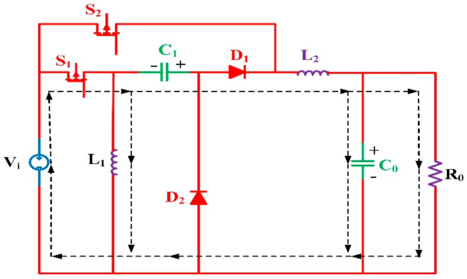
2.1. The Hybrid DC-DC Zeta Converter Operating Principle
- All semiconductor devices, such as MOSFETs and diodes, are considered ideal.
- Two capacitors, C1 and C2, are substantial enough to maintain a constant voltage.
- I.
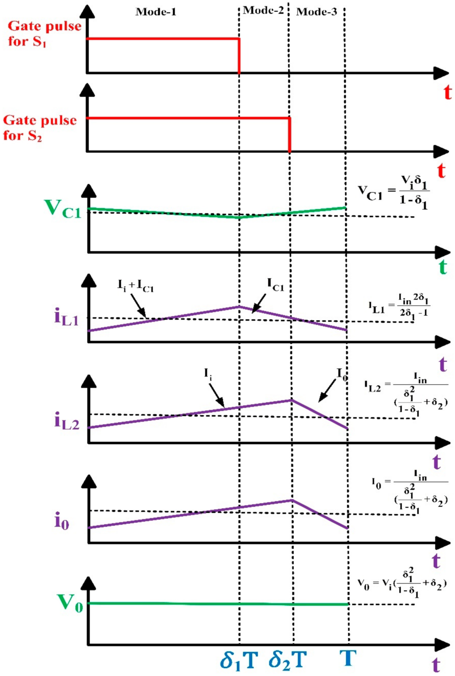
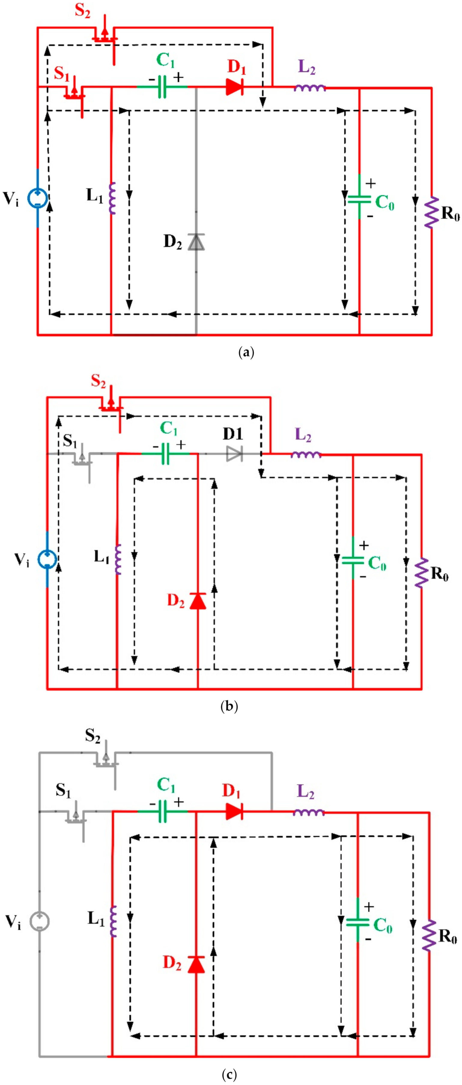
- Mode-1 (0 < t < δ1T): In this mode Switch S1 and S2 are turned ON and Vi is in parallel with inductor L1, so the voltage across inductor L1 is equal to the Vi. L1 is charged through Vi, and L2 is charged through Vi + VC1 and capacitor C1 is discharged through L2 + V0, which are illustrated in Figure 3a. As a result, the following equations can be obtained:
- II.
- Mode 2 (δ1T < t < δ2T): Switch S1 is turned OFF, while switch S2 is switched ON in this mode. L1 is discharged through VC1, L2 is charged through Vi, and capacitor C1 is charged through L1 as illustrated in Figure 3b. The inductor voltages can be computed as
- III.
- Mode-3 (δ2T < t < T): In this mode, two switches are turned OFF. L1 is discharged through VC1, and L2 is discharged through V0, and capacitor C1 is charged through L1 as in Figure 3c. The inductor voltages can be computed as
2.2. Steady-State Analysis of the Converter
2.2.1. Voltage Gain Analysis
2.2.2. Dynamic Modelling
2.3. Passive Component Design and Efficiency Calculation
2.3.1. Inductor Design
2.3.2. Capacitor Design
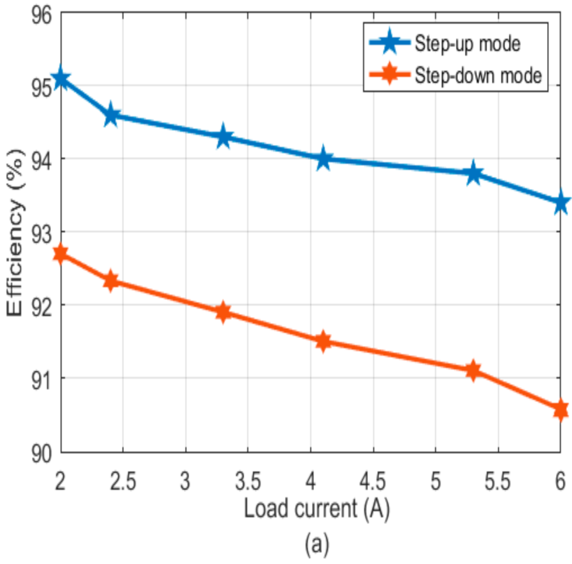
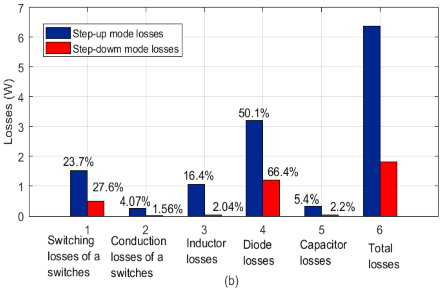
2.3.3. Efficiency Calculations
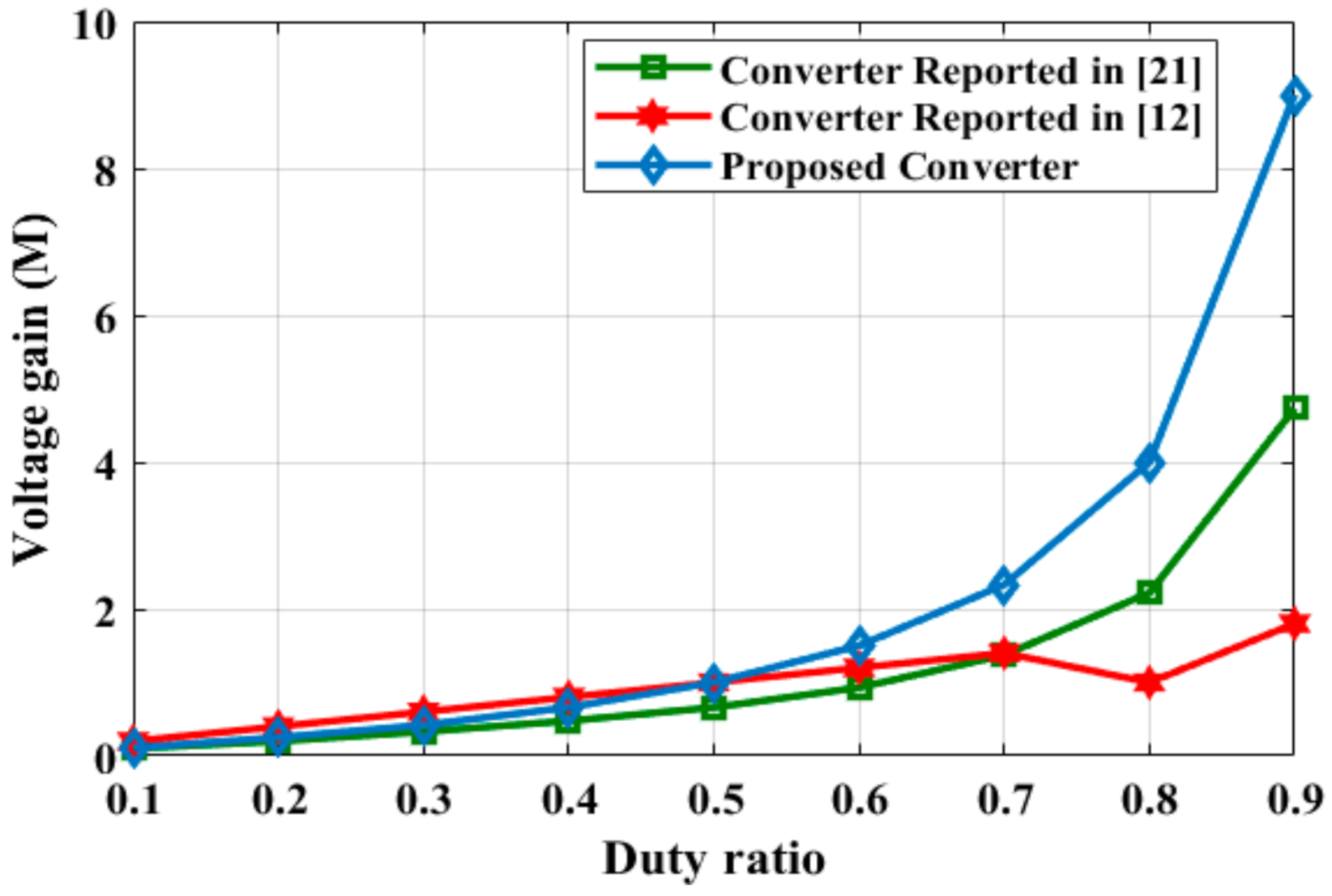
2.4. Comparison with Other Topologies
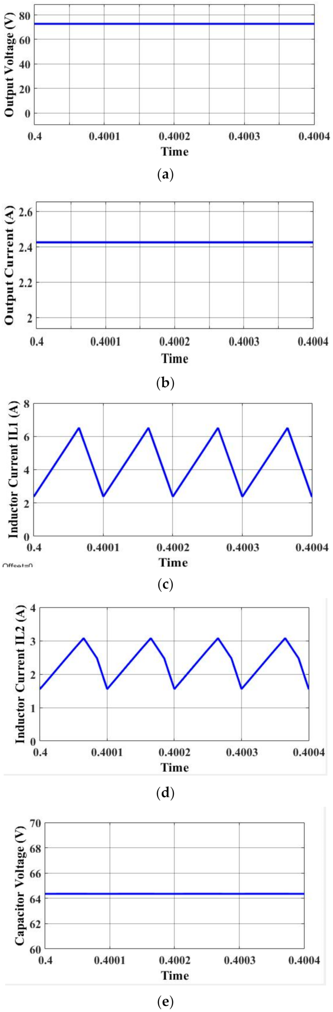
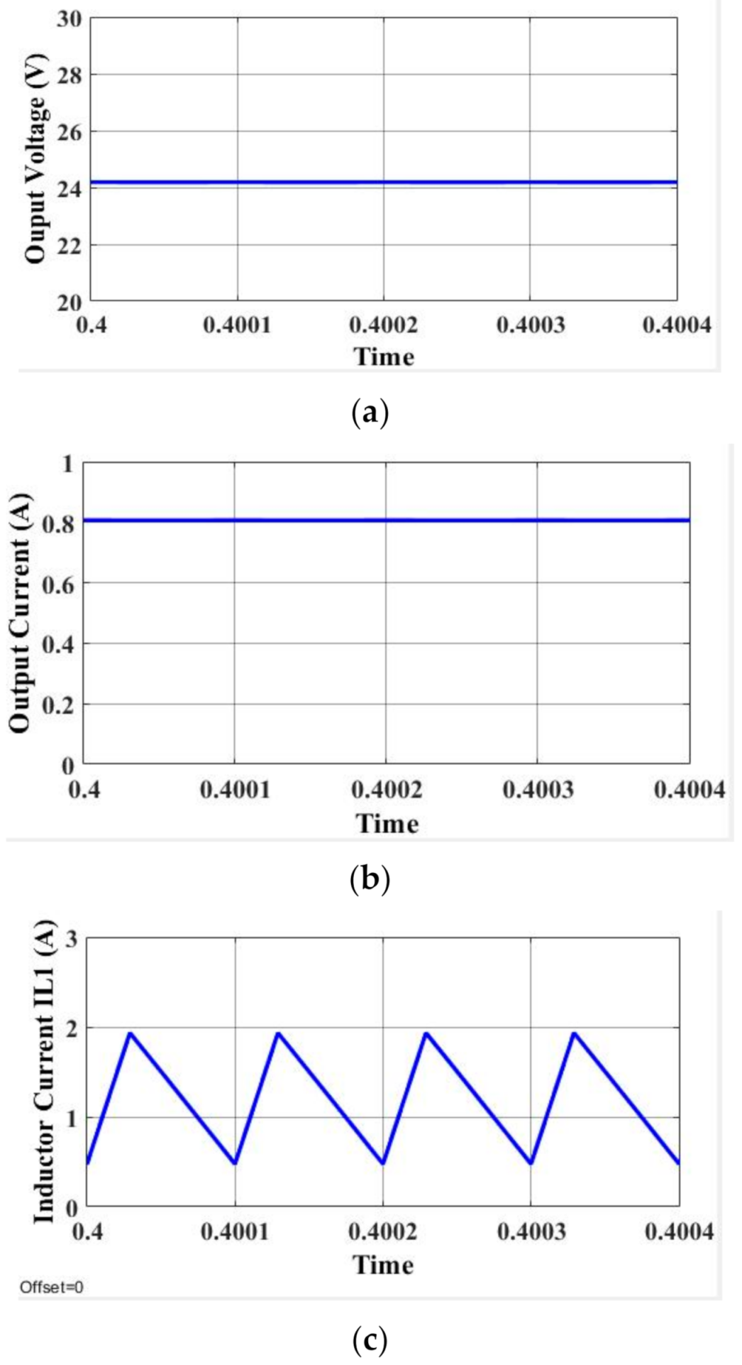
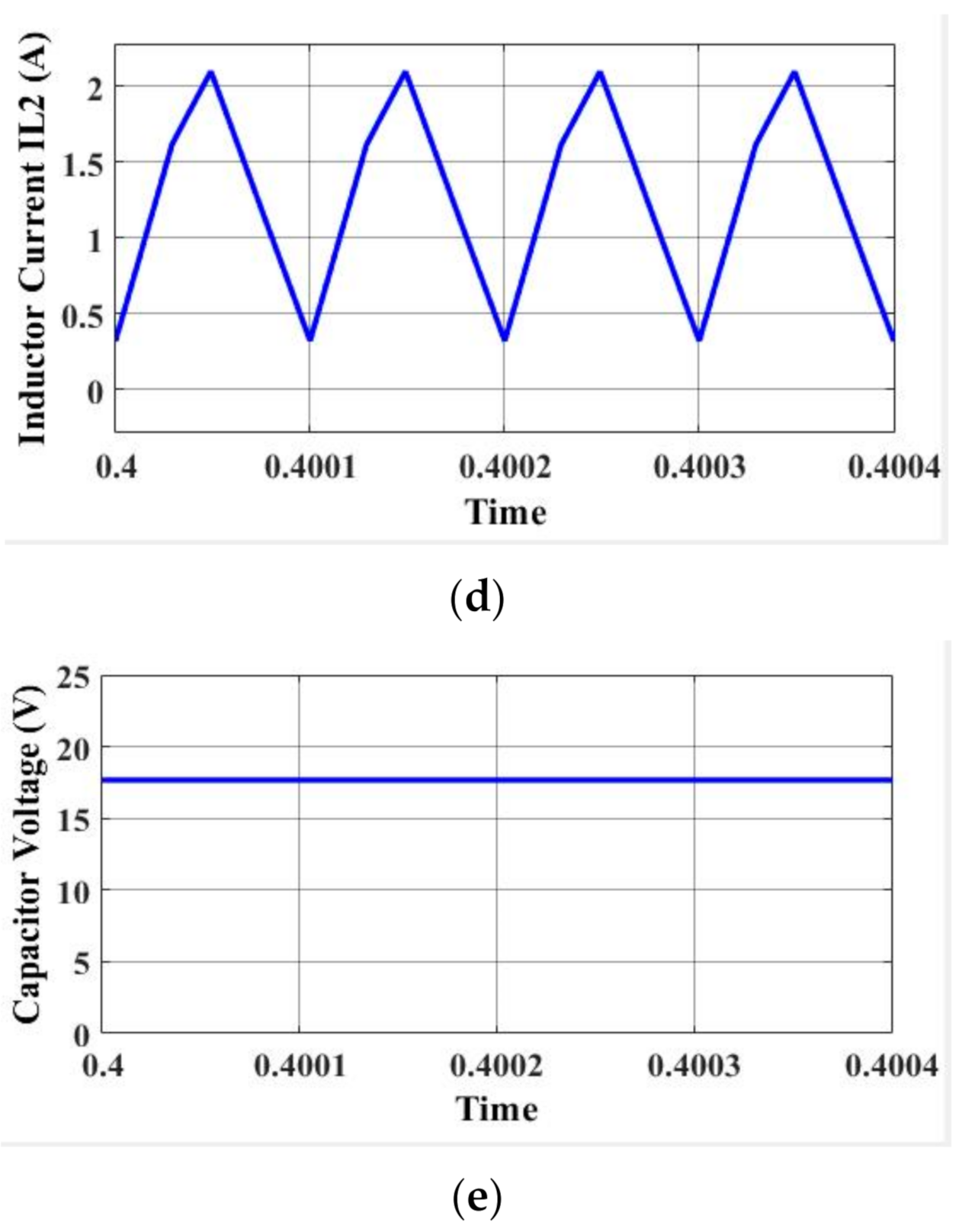
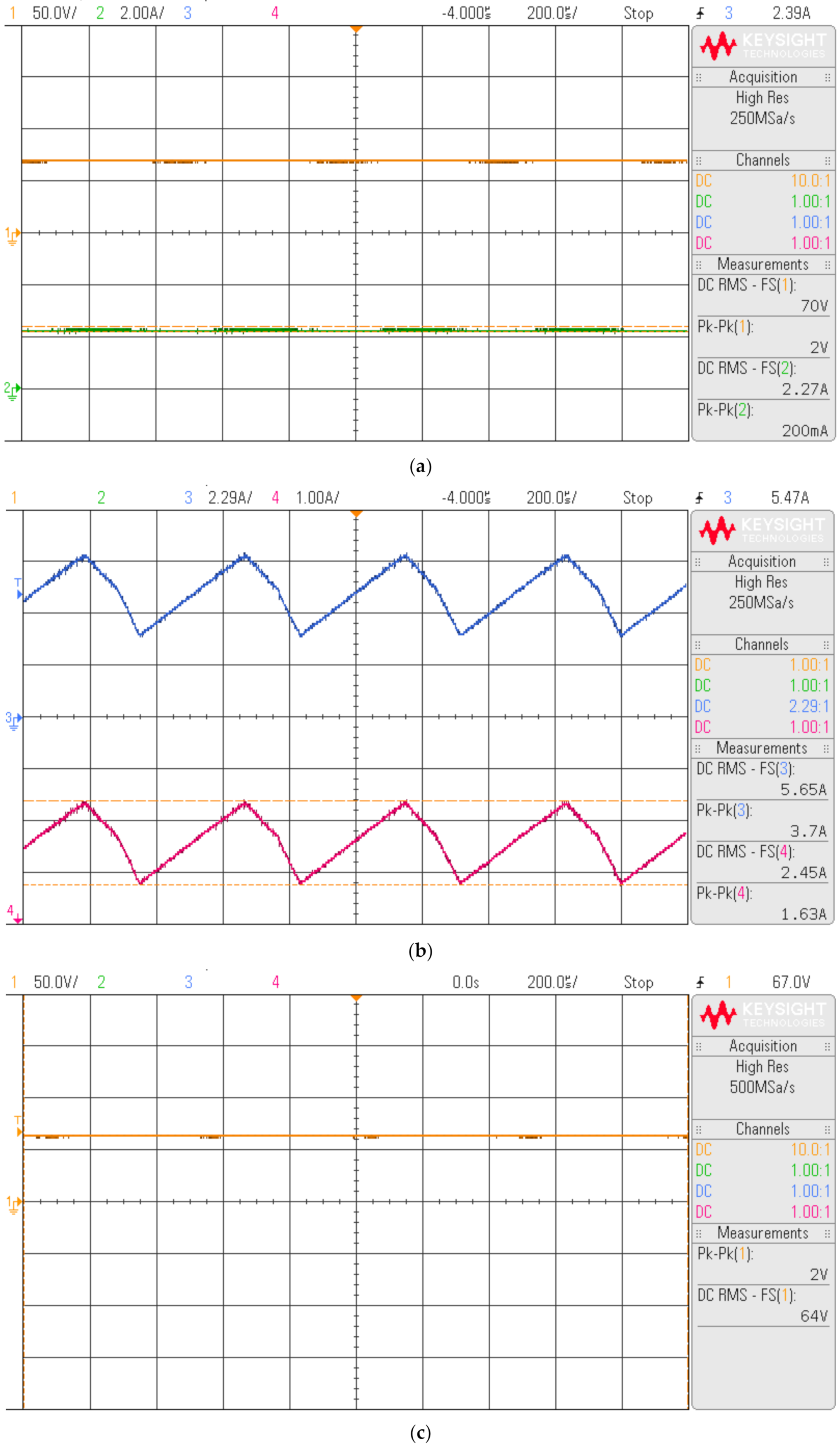
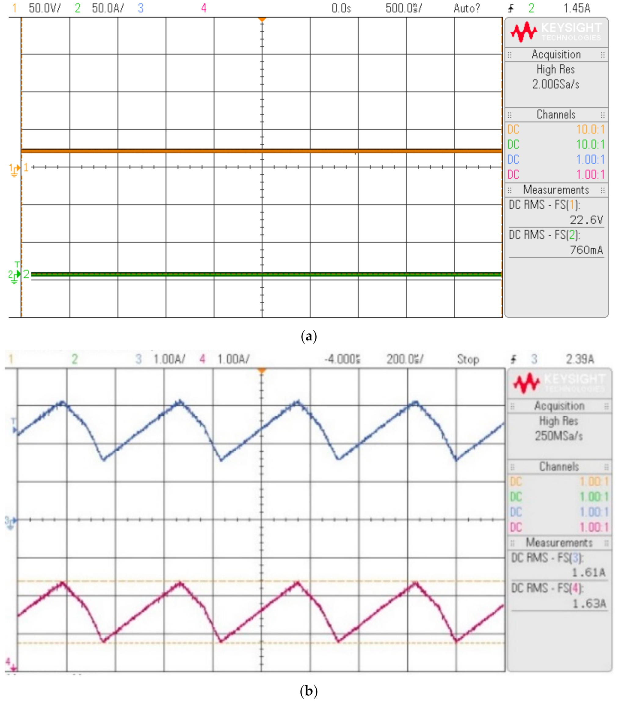
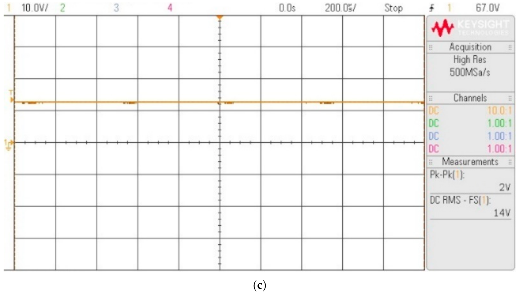
3. Results
4. Conclusions
Author Contributions
Funding
Institutional Review Board Statement
Informed Consent Statement
Data Availability Statement
Acknowledgments
Conflicts of Interest
References
- Lee, H.-S.; Choe, H.-J.; Ham, S.-H.; Kang, B. High-Efficiency Asymmetric Forward-Flyback Converter for Wide Output Power Range. IEEE Trans. Power Electron. 2017, 32, 433–440. [Google Scholar] [CrossRef]
- Hwu, K.I.; Jiang, W.Z. Voltage Gain Enhancement for a Step-up Converter Constructed by KY and Buck-Boost Converters. IEEE Trans. Ind. Electron. 2014, 61, 1758–1768. [Google Scholar] [CrossRef]
- Ajami, A.; Ardi, H.; Farakhor, A. Design, Analysis and Implementation of a Buck–Boost DC/DC Converter. IET Power Electron. 2014, 7, 2902–2913. [Google Scholar] [CrossRef]
- Rayeen, Z.; Hanif, O.; Bose, S. Modelling and Analysis of Interleaved Cuk Converter Controlled by PID Controller with Phase Shift PWM Method. In Proceedings of the 2019 IEEE Students Conference on Engineering and Systems (SCES), Allahabad, India, 29–31 May 2019. [Google Scholar]
- Banaei, M.R.; Bonab, H.A.F. A High Efficiency Non isolated Buck–Boost Converter Based on ZETA Converter. IEEE Trans. Ind. Electron. 2020, 67, 1991–1998. [Google Scholar] [CrossRef]
- Ansari, S.A.; Moghani, J.S. A Novel High Voltage Gain Noncoupled Inductor SEPIC Converter. IEEE Trans. Ind. Electron. 2019, 66, 7099–7108. [Google Scholar] [CrossRef]
- Axelrod, B.; Berkovich, Y.; Ioinovici, A. Switched-Capacitor/Switched-Inductor Structures for Getting Transformerless Hybrid DC–DC PWM Converters. IEEE Trans. Circuits Syst. I Regul. Pap. 2008, 55, 687–696. [Google Scholar] [CrossRef]
- Liao, H.-K.; Liang, T.-J.; Yang, L.-S.; Chen, J.-F. Non-Inverting Buck–Boost Converter with Interleaved Technique for Fuel-Cell System. IET Power Electron. 2012, 5, 1379. [Google Scholar] [CrossRef]
- Fu, J.; Zhang, B.; Qiu, D.; Xiao, W. A Novel Single-Switch Cascaded DC-DC Converter of Boost and Buck-Boost Converters. In Proceedings of the 2014 16th European Conference on Power Electronics and Applications, Lappeenranta, Finland, 26–28 August 2014. [Google Scholar]
- Miao, S.; Wang, F.; Ma, X. A New Transformer less Buck–Boost Converter with Positive Output Voltage. IEEE Trans. Ind. Electron. 2016, 63, 2965–2975. [Google Scholar] [CrossRef]
- Wu, H.; Sun, K.; Chen, L.; Zhu, L.; Xing, Y. High Step-up/Step-down Soft-Switching Bidirectional DC–DC Converter with Coupled-Inductor and Voltage Matching Control for Energy Storage Systems. IEEE Trans. Ind. Electron. 2016, 63, 2892–2903. [Google Scholar] [CrossRef]
- Hwu, K.I.; Yau, Y.T. Two Types of KY Buck–Boost Converters. IEEE Trans. Ind. Electron. 2009, 56, 2970–2980. [Google Scholar] [CrossRef]
- Lin, B.-R.; Chen, J.-J. Analysis of an Integrated Flyback and Zeta Converter with Active Clamping Technique. IET Power Electron. 2009, 2, 355–363. [Google Scholar] [CrossRef]
- Valsalan, N.; Subha, S.T. Dual Zeta Converter with Reduced Ripple for Sensitive Load Applications. In Proceedings of the 2013 International Conference on Energy Efficient Technologies for Sustainability, Nagercoil, India, 10–12 April 2013. [Google Scholar]
- Saadat, P.; Abbaszadeh, K. A Single-Switch High Step-up DC–DC Converter Based on Quadratic Boost. IEEE Trans. Ind. Electron. 2016, 63, 7733–7742. [Google Scholar] [CrossRef]
- Ding, S.; Wang, F. A New Negative Output Buck–Boost Converter with Wide Conversion Ratio. IEEE Trans. Ind. Electron. 2017, 64, 9322–9333. [Google Scholar] [CrossRef]
- Banaei, M.R.; Ghabeli Sani, S. Analysis and Implementation of a New SEPIC-Based Single Switch Buck-Boost Dc-Dc Converter with Continuous Input Current. IEEE Trans. Power Electron. 2018, 33, 10317–10325. [Google Scholar] [CrossRef]
- Banaei, M.R.; Bonab, H.A.F. A Novel Structure for Single-Switch Nonisolated Transformerless Buck–Boost DC–DC Converter. IEEE Trans. Ind. Electron. 2017, 64, 198–205. [Google Scholar] [CrossRef]
- Banaei, M.R.; Ardi, H.; Farakhor, A. Analysis and Implementation of a New Single-switch Buck–Boost DC/DC Converter. IET Power Electron. 2014, 7, 1906–1914. [Google Scholar] [CrossRef] [Green Version]
- Moradpour, R.; Ardi, H.; Tavakoli, A. Design and Implementation of a New SEPIC-Based High Step-up DC/DC Converter for Renewable Energy Applications. IEEE Trans. Ind. Electron. 2018, 65, 1290–1297. [Google Scholar] [CrossRef]
- Li, J.; Liu, J. A Novel Buck–Boost Converter with Low Electric Stress on Components. IEEE Trans. Ind. Electron. 2019, 66, 2703–2713. [Google Scholar] [CrossRef]


| Converter Topology | Proposed Converter | Reported in [12] | Reported in [21] | Reported in [18] | Traditional Zeta Converter |
|---|---|---|---|---|---|
| Number of switches | 2 | 2 | 1 | 1 | 1 |
| Number of diodes | 2 | 1 | 3 | 3 | 1 |
| Number of inductors | 2 | 2 | 2 | 3 | 2 |
| Number of capacitors | 2 | 3 | 2 | 5 | 2 |
| Total component count | 8 | 8 | 8 | 12 | 6 |
| Input current | Continuous | Continuous | Continuous | Discontinuous | Continuous |
| Voltage gain |
| Components | Range |
|---|---|
| Inductor L1 | 1 mH, RL = 35 m Ω |
| Inductor L2 | 1 mH, RL = 40 m Ω |
| Capacitor C0 | 10 µH, RL = 0.051 Ω |
| Capacitor C1 | 100 µH, RL = 0.02 Ω |
| Vin, f | 36 V, 10 KHz |
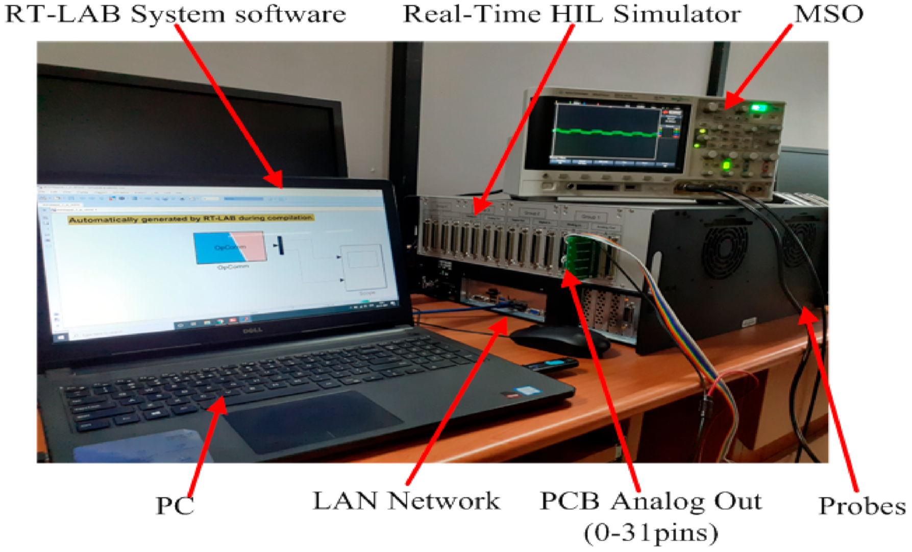
| Name of the Device | OP5700 Simulator |
|---|---|
| FPGA | Xilinx® Virtex®7 FPGA on VC707 board s |
| I/O Lines | 256 lines, routed to eight analog or digital, 16 or 32 channels |
| High-Speed Communication Ports | 16SFP sockets, up to 5 GBps |
| I/O Connectors | Four-panel of 4 DB37 connectors |
| Monitoring Connectors | Four-panel of RJ45 connectors |
| PC Interface | Standard PC connectors |
| Power Rating | Input: 100-240VAC, 50–60 Hz, 10/5 A Power: 600 W |
| Limitations |
|---|
|
Publisher’s Note: MDPI stays neutral with regard to jurisdictional claims in published maps and institutional affiliations. |
© 2022 by the authors. Licensee MDPI, Basel, Switzerland. This article is an open access article distributed under the terms and conditions of the Creative Commons Attribution (CC BY) license (https://creativecommons.org/licenses/by/4.0/).
Share and Cite
Santosh Kumar Reddy, P.L.; Obulesu, Y.P.; Singirikonda, S.; Al Harthi, M.; Alzaidi, M.S.; Ghoneim, S.S.M. A Non-Isolated Hybrid Zeta Converter with a High Voltage Gain and Reduced Size of Components. Electronics 2022, 11, 483. https://doi.org/10.3390/electronics11030483
Santosh Kumar Reddy PL, Obulesu YP, Singirikonda S, Al Harthi M, Alzaidi MS, Ghoneim SSM. A Non-Isolated Hybrid Zeta Converter with a High Voltage Gain and Reduced Size of Components. Electronics. 2022; 11(3):483. https://doi.org/10.3390/electronics11030483
Chicago/Turabian StyleSantosh Kumar Reddy, Padala Lakshmi, Yeddula Pedda Obulesu, Srinivas Singirikonda, Mosleh Al Harthi, Mohammed S. Alzaidi, and Sherif S. M. Ghoneim. 2022. "A Non-Isolated Hybrid Zeta Converter with a High Voltage Gain and Reduced Size of Components" Electronics 11, no. 3: 483. https://doi.org/10.3390/electronics11030483