1. Introduction
Recently, high-speed and large-capacity data processing has become important in the fields of big data and artificial intelligence, which are the core of the fourth industrial revolution. Conventional random-access memory devices, such as static random-access memory (SRAM) and dynamic random-access memory (DRAM), store data during a write cycle and read a stored memory during a read cycle. As a specific memory location, called the address, must be assigned during this process, sequential memory operations are inevitable for random-access memory devices [
1,
2,
3,
4,
5].
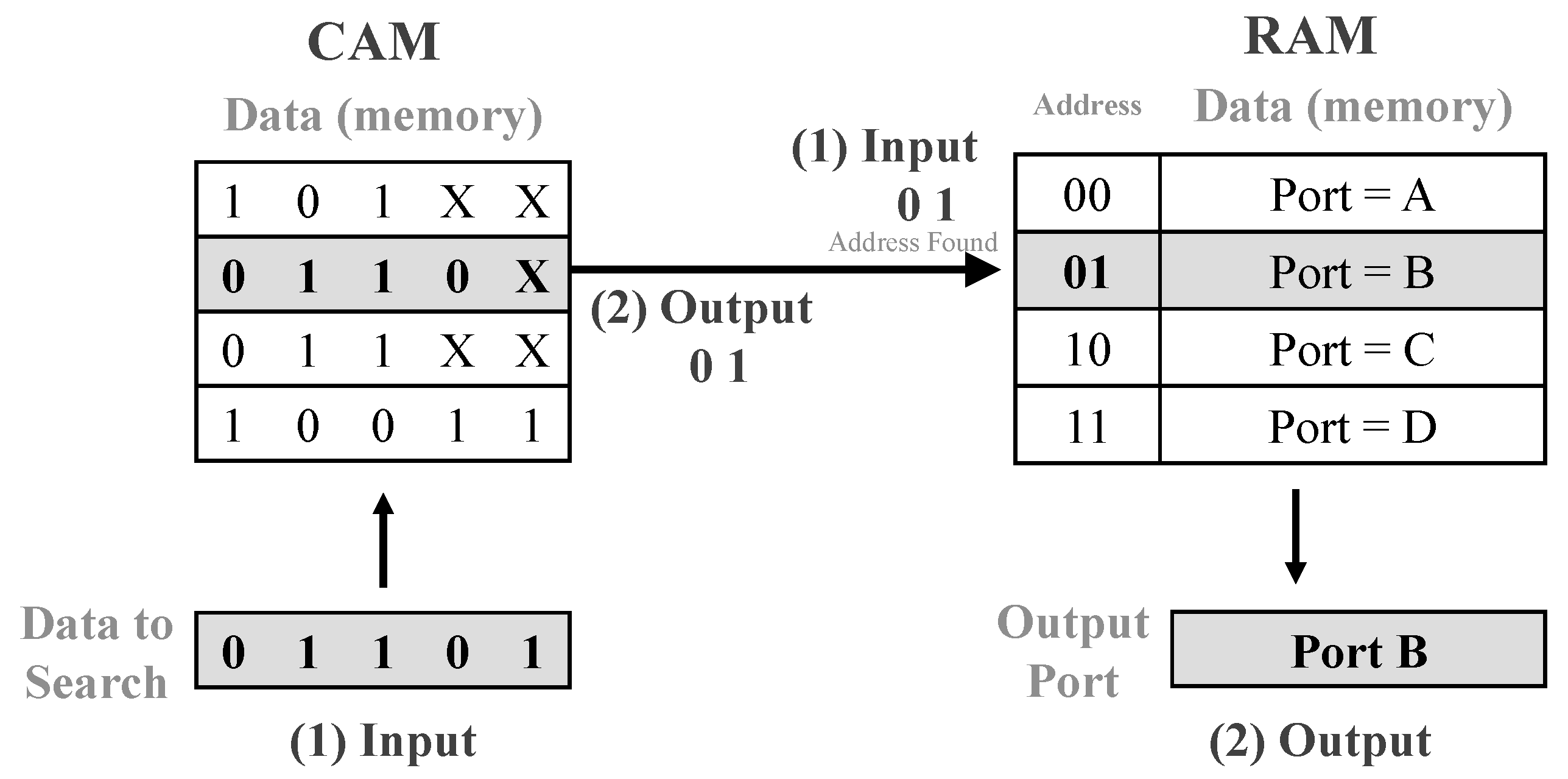
For this reason, conventional random-access memory devices are not suitable for the high-speed and low-power large-capacity data processing required for big data and artificial intelligence. When search data are input, content-addressable memory (CAM), which this study focuses on, compares the search data against all data stored in the data array simultaneously in parallel. The CAM quickly returns the matching address values to the output to enable a high-speed search operation, as shown in
Figure 1 [
6,
7]. For conventional CMOS-based CAMs, nine to ten metal-oxide–semiconductor field-effect transistors (MOSFETs) are used for BCAMs, and 16–17 MOSFETs are used for TCAMs, as shown in
Figure 2. Hence, CAMs have a significantly lower density than SRAMs, which consist of six to eight MOSFETs. It is not possible to manufacture high-capacity memory with existing CMOS-based CAMs because they have a lower density than SRAMs/DRAMs. In addition, CAMs have a power-consumption problem. Many recent studies have proposed structures for high-speed and low-power CAMs [
8,
9,
10,
11,
12,
13,
14,
15,
16,
17,
18,
19,
20,
21].
More recently, the possibility of a TCAM cell using a single NEM device has been proposed in [
22]. Applications of NEM-based TCAM arrays are proposed, and devices and model-based operations are validated in [
23,
24]. In [
23], a compact TCAM cell by removing search line transistors is proposed for small area. A new simple TCAM searching method for neural network applications is proposed in [
24].
In this study, three-dimensional integrated nanoelectromechanical (NEM) memory switches, which are driven by an electromechanical principle, are used in place of conventional CMOS transistors to overcome the limitations of CMOS-based CAMs and increase the density of the front-end area [
25,
26,
27]. This work is an extension of [
22], and is proposing a new CAM architecture with an advanced precharge circuit to improve stability in practical operation for both BCAM and TCAM by using a single NEM cell. In order to validate the performance of the proposed CAM array as a practical memory system, the proposed cell is extended to 10 rows of 10-bit array. Layout simulations are conducted to verify the operation and the higher performance over CMOS-based counterparts. An actual chip is manufactured in 65 nm technology, and the CAM operation is successfully measured.
The remainder of the paper is structured as follows.
Section 2 introduces the conventional SRAM-based CAM. The architecture and the periphery circuitry of the proposed NEM-based CAM are discussed in
Section 3.
Section 4 validates the performance of the 10 × 10 CAM array through simulations. Chip layout and actual measurement are discussed in
Section 5.
Section 6 concludes this work.
2. Related Work
CAMs have three modes: write, read, and search. They operate in the same manner as SRAMs in the write and read modes. For example, to store a ‘1’ in a memory cell, a ‘1’ is written to the BL, and a high signal is applied to the WL. Here, the access transistors, N6 and N7, are turned on, so the data written to the BL are stored in the cell. When a low signal is applied to WL, the access transistor turns off, and a circuit consisting of two inverters stores data. To read the bit stored in the SRAM, a high signal is applied to the WL while the BL is precharged. If ‘0’ is stored, BL is discharged to ground (GND) and indicates a low value. If ‘1’ is stored in SRAM, the precharged high value is maintained.
In the CAM search operation, both search lines (SL, SLB) are precharged with GND, and the ML is precharged with the supply voltage (VDD) value. The data value being searched for is written to the SL. If the data value being searched for, using the N1–N4 transistors, and the data value stored in the SRAM are found to be the same, the pull-down path is kept ‘off’, and the ML has a high value, indicating a ‘match’. Conversely, if the value being searched for and the stored data value differ, one of the pull-down paths connects the ML to GND and the ML is discharged to a low state, indicating a ‘mismatch’.
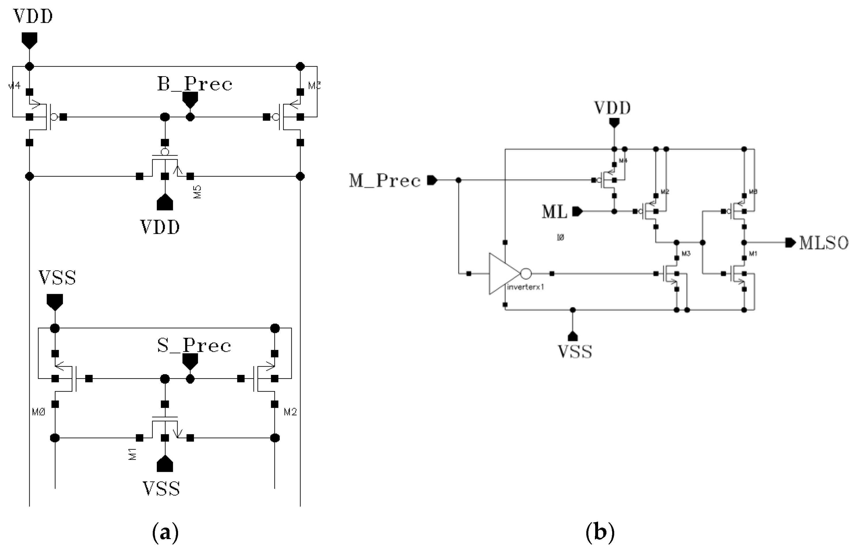
In conventional CMOS-based CAMs, a precharge circuit is used to reduce the delay, as shown in
Figure 3 [
4,
5]. When the BL or ML voltage decreases in the precharged state during an operation, owing to the precharge circuit, the delay problem can be solved by using a sense amplifier to detect small changes [
8].
The formula for calculating the delay is as follows.
increases as the number of cells increases, and
has a small value because of the high-density characteristics of the cells. Therefore, the change of
must be rapidly minimized to have a small delay value.
In addition, if the SL precharge is used, the two NMOSs connected in series in the matching circuit are turned off before a match operation is performed. Hence, the pull-down path that connects the ML to GND is blocked to prevent a discharge. In addition to these tactics, studies have been conducted on various methods to reduce power consumption; for example, a precharge-free CAM circuit that eliminates the precharge circuit to reduce power consumption when a mismatch occurs [
24] or a CAM circuit using an AND gate that yields ‘1’ when all bits are ‘1’ and yields ‘0’, if even one bit does not match [
25].
2.1. CMOS-Based BCAM and TCAM
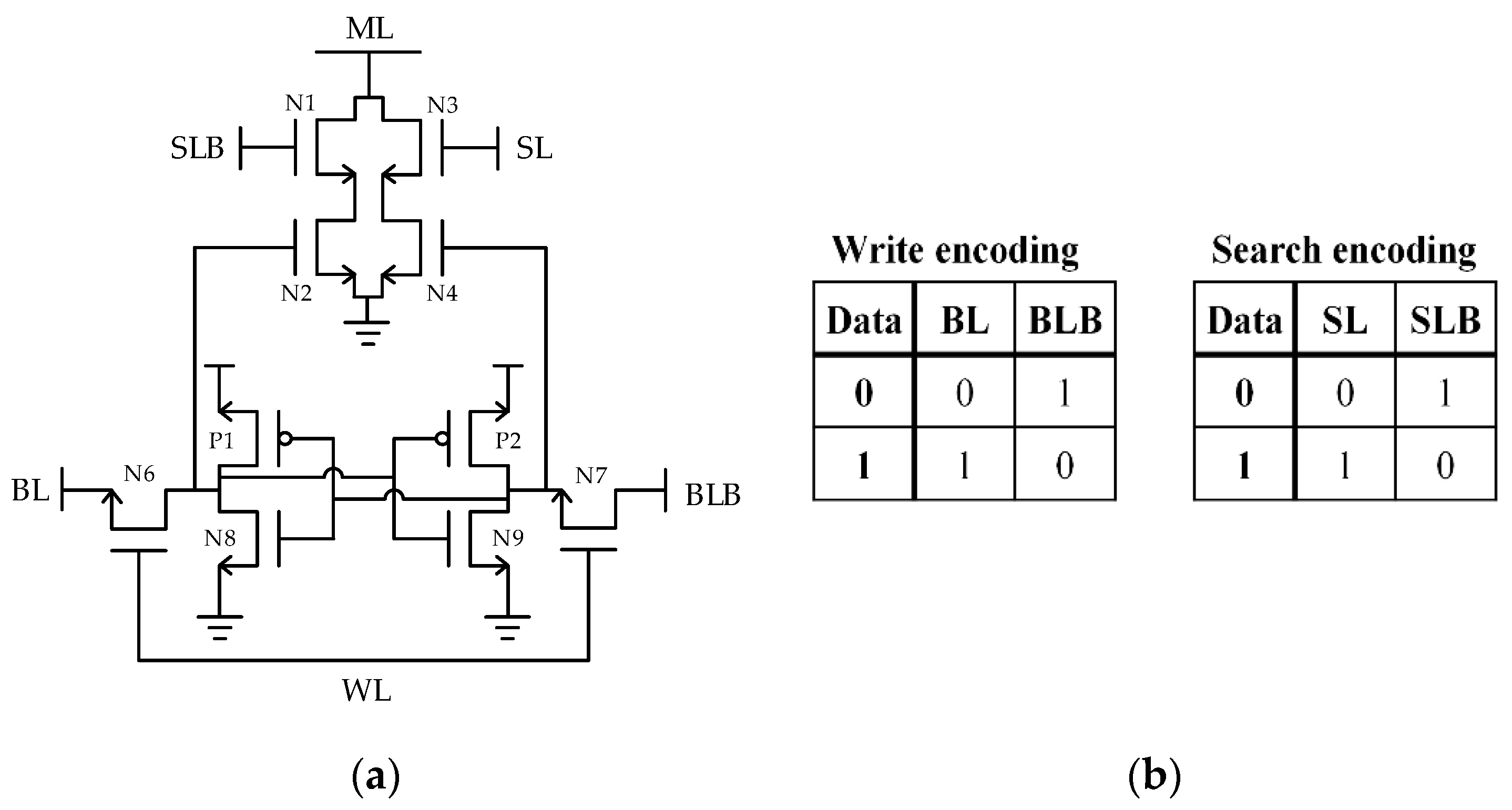
A typical CMOS-based BCAM uses one SRAM to store a value of ‘0’ or ‘1’. A schematic diagram of the CMOS-based BCAM single-bit cell is shown in
Figure 4a, and the data encoding is depicted in
Figure 4b. The transistor sizing values for the CMOS-based BCAM single-bit cell are summarized in
Table 1 [
3].
In the CMOS-based BCAM single-bit cell, six transistors are used in the memory cell, and four transistors with pass-transistor logic are used for the search operation. Two additional transistors are used for the write operation. The upper CAM cell for the match operation uses four transistors, and the SL and BL each require three transistors for the precharge [
4,
5]. A total of 22 transistors was used in the CMOS-based BCAM.
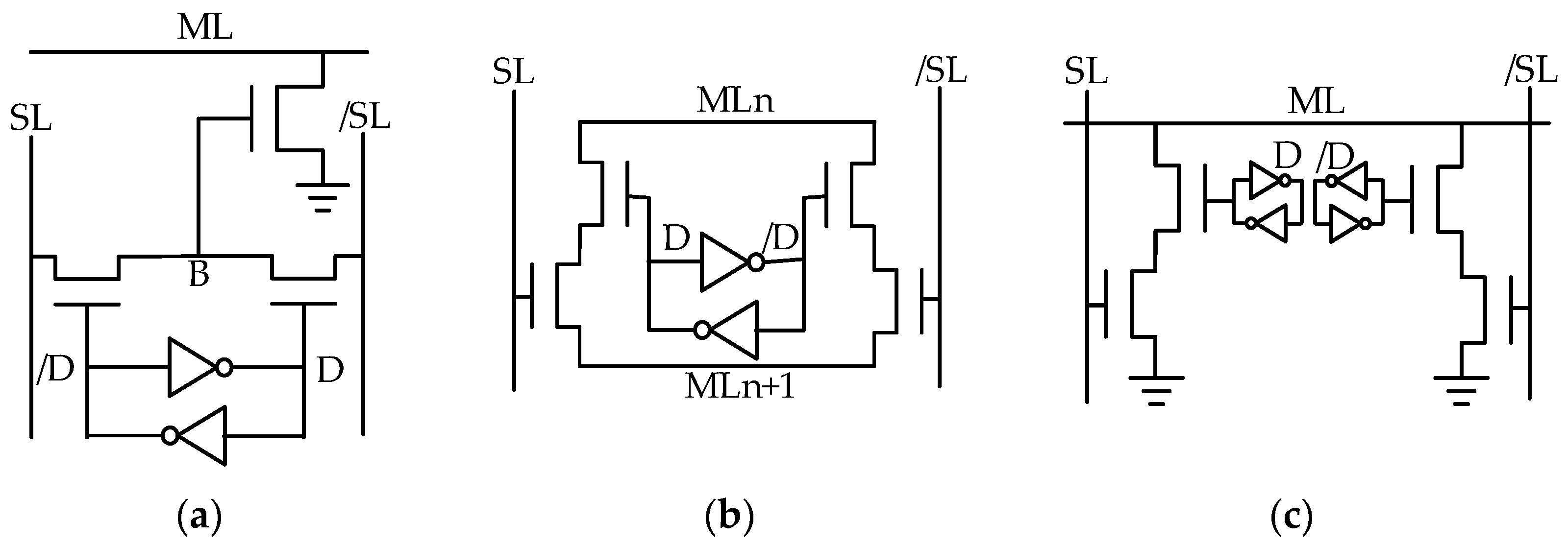
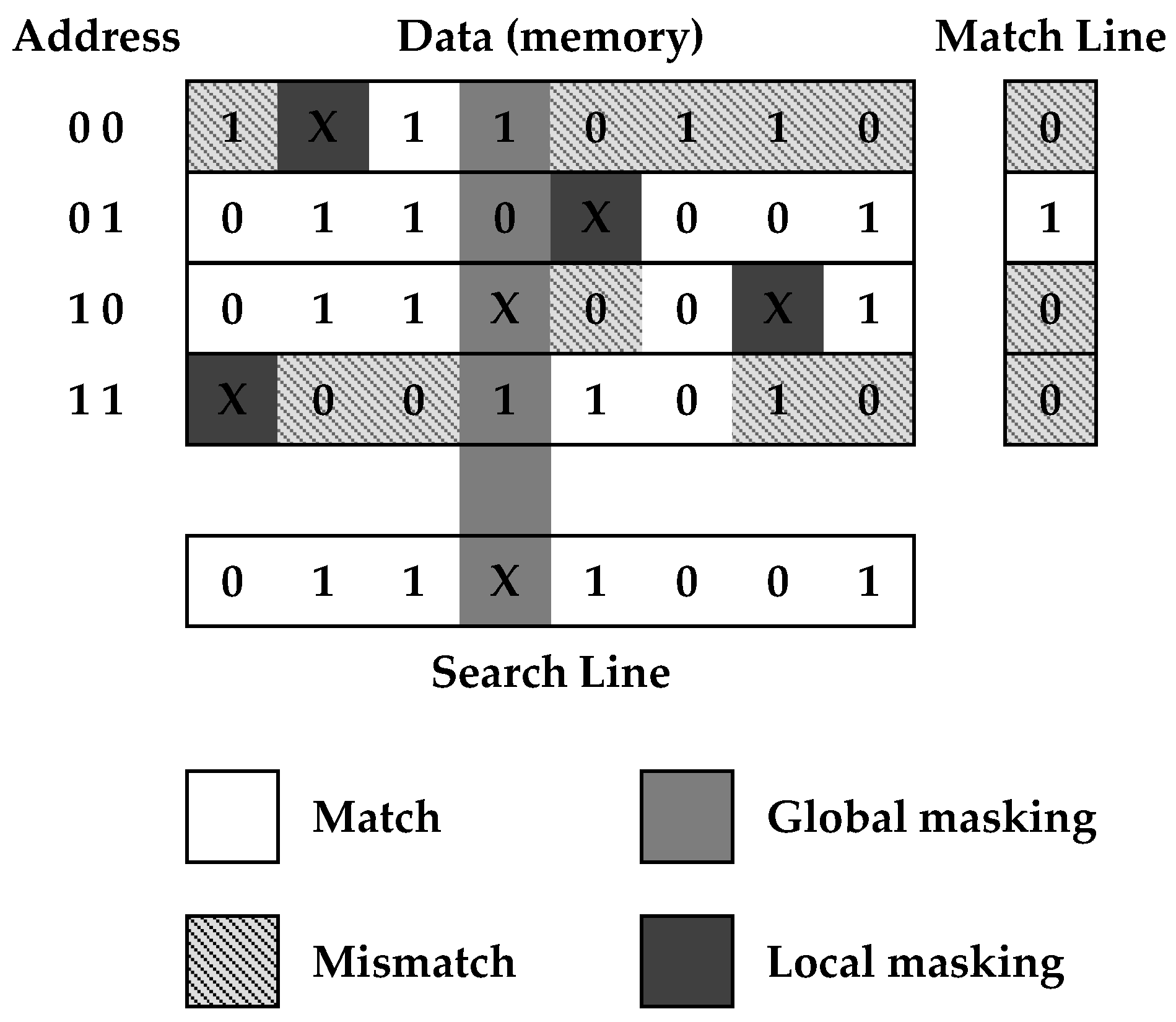
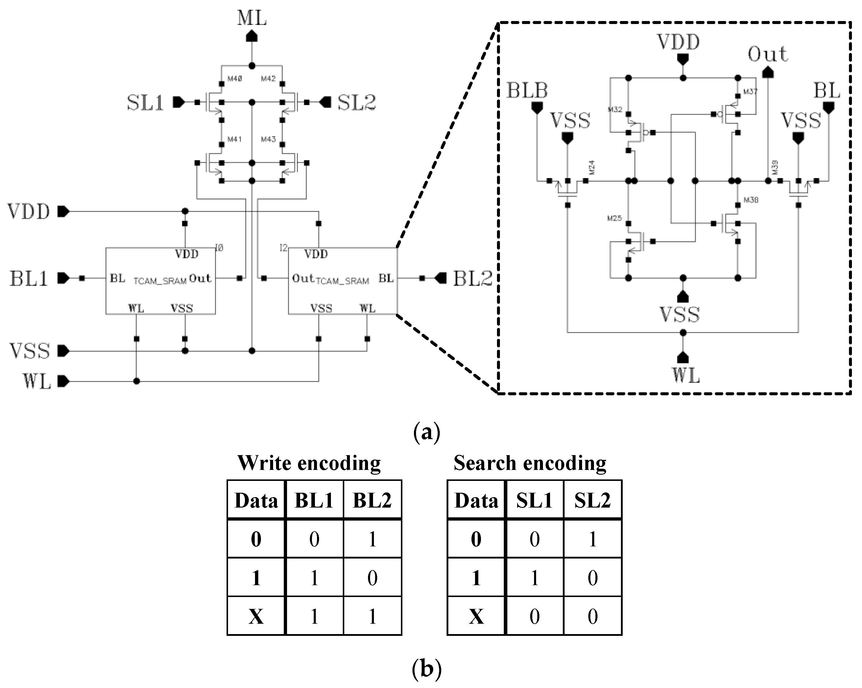
A conventional CMOS-based ternary CAM uses two SRAM cells to store ‘0’, ‘1’, and ternary value X (do not care). The X value can be applied to both a data write and a search as a bit mask. When an X value is written, the cell always returns a match when searching, and when the X value is searched, the cell returns a match with whatever data is written in the cell. Writing an X value can be referred to as local masking and searching for an X value is global masking. As shown in
Figure 5, local masking applies masking to one specific cell, while global masking applies masking to an entire column. The schematic design of a CMOS-based TCAM cell is shown in
Figure 6, with data encodings for data values on write and search. ‘0’ is a low and ‘1’ is a high value (e.g., VDD) input. The data-search functions are the same as in BCAM; however, the X value is also considered. When the X value ‘11’ is written, an inverse voltage value ‘00’ is passed to the lower pair of NMOS search circuits, disconnecting the ML from the pull-down path, regardless of the SL. When the X value ‘00’ is searched, the upper pair of NMOS transistors disconnect the pull-down path.
While the SL and ML precharge circuits are the same as those for BCAM, TCAM requires two BL precharge circuits for each memory-array column, as two independent SRAM cells are used for each TCAM cell. Two 6T SRAM cells and four transistors are used for the search circuit, making a total of 16 transistors for each SRAM-TCAM cell. In addition, two 7T BL precharge circuits, one 9T SL precharge circuit (excluding the buffer), and one 7T ML precharge circuit are used to form a fully functional CMOS-based TCAM, using 46 transistors in total.
2.2. NEM Memory Switch
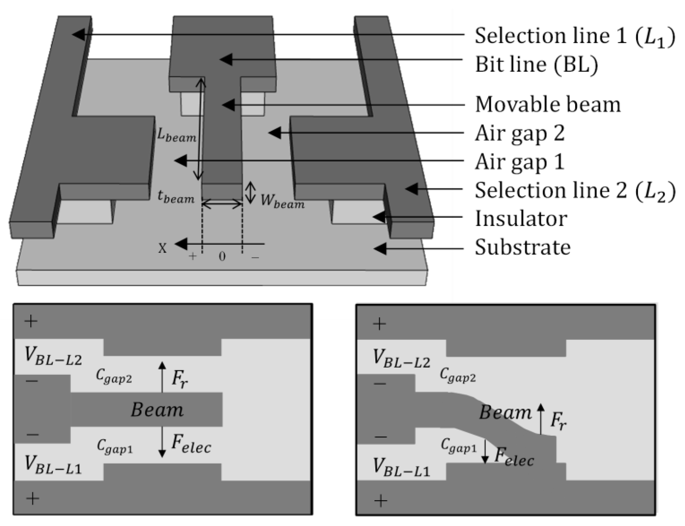
Figure 7 is a 3D depiction and a cross-section of a nanoelectromechanical memory switch driven by an electromechanical principle using an air gap-based smart wiring technology implemented on an existing CMOS circuit [
25]. The NEM memory switch connects the path by controlling the central movable beam. A movable beam that has moved once is non-volatile, and maintains the path after writing the data, owing to the van der Waals adhesion force [
25,
26,
27]. For example, when a sufficient voltage is applied to
L1, the beam forms a path with
L1, and when sufficient voltage is applied to
L2, the beam forms a path to
L2. Additionally, there is a floating state that is not connected to either
L1 or
L2, and can have a total of three configurable states. These characteristics of NEM memory are especially valuable when designing TCAM. Thus, NEM memory allows TCAM designs with a small number of transistors and can be built on top of the CMOS logic layer to achieve very high densities. In addition, since the state is changed by the physical connection of the movable beam, there is no need for switching, which has the advantage of lower power consumption compared to CMOS-based.
Section 3 describes the single cell and structure of the NEM-based CAM by utilizing the characteristics of the NEM memory switch.
3. Proposed NEM-Based CAM Designs
In this study, a NEM memory-switch device, utilizing a CMOS back-end-of-the-line (BEOL) process, is applied to a high-speed, low-power CAM device using a commercial 65-nm process. By doing so, this study aims to improve the problems that have occurred when implementing high-capacity, low-power systems, owing to the low density of a typical CMOS-based CAM.
Therefore, we propose a CAM single-bit cell and 10 × 10 CAM array structure using a NEM memory switch, which utilizes the CMOS BEOL process. The process uses a three-dimensional integrated NEM memory switch, driven by an electromechanical principle, using air-gap-based smart-wiring technology implemented on a CMOS circuit [
25].
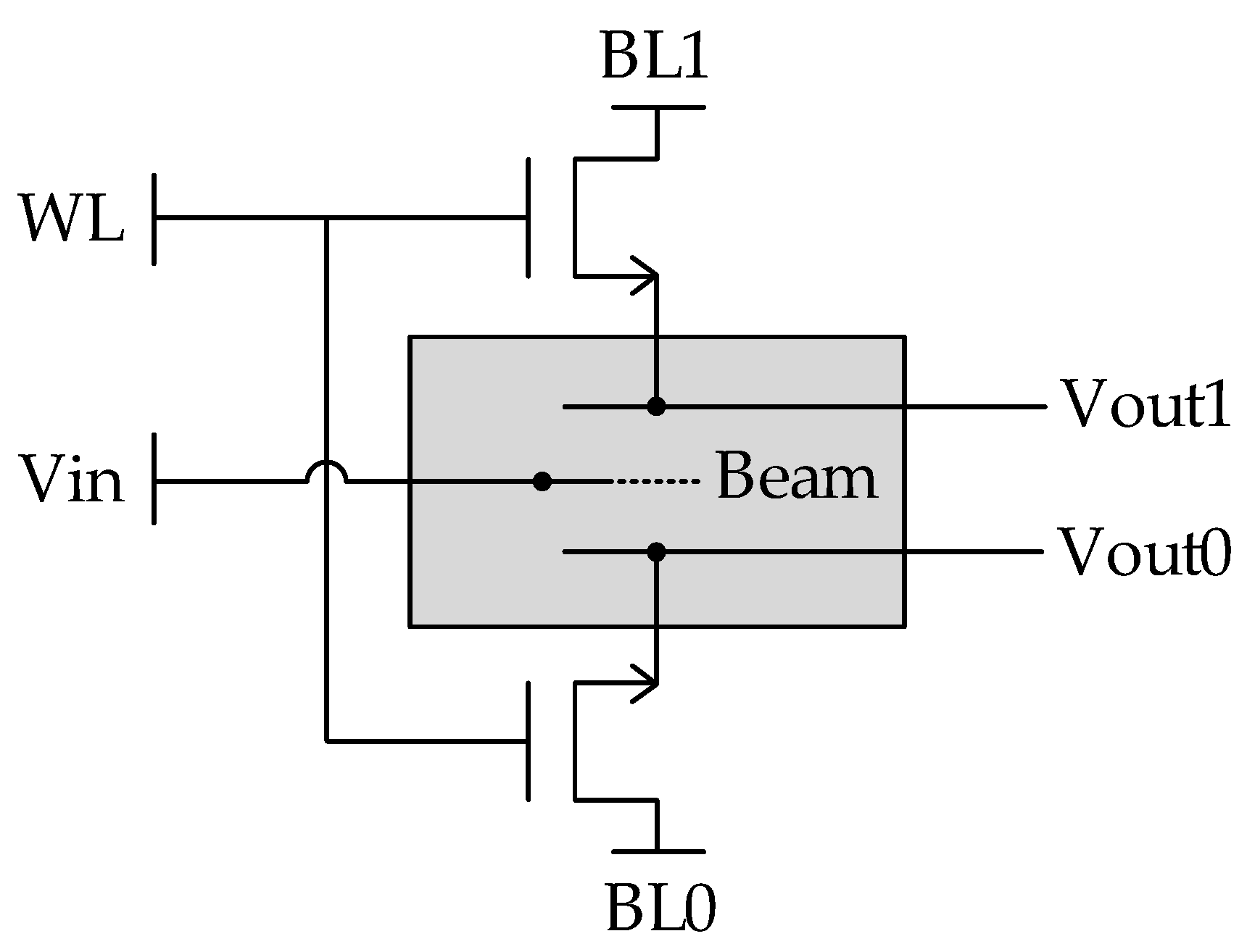
Figure 8 shows the schematic of the memory cell implemented using the NEM memory switch. When a data-write operation is performed, a voltage is applied to the bit lines (BL0, BL1) of the NEM memory switch to establish a beam connection. Subsequently, a high value is applied to Vin of the NEM memory switch during the search operation, and the voltage delivered to Vout0 and Vout1 can be checked (the voltage applied to Vin is delivered through the path where the beam is connected). In short, the stored states can be checked.
NEM-Based CAM
With conventional CMOS-based CAMs, BCAMs and TCAMs must be implemented separately. On the other hand, with the NEM-based CAM proposed in this paper, both BCAMs and TCAMs can be implemented with the same structure.
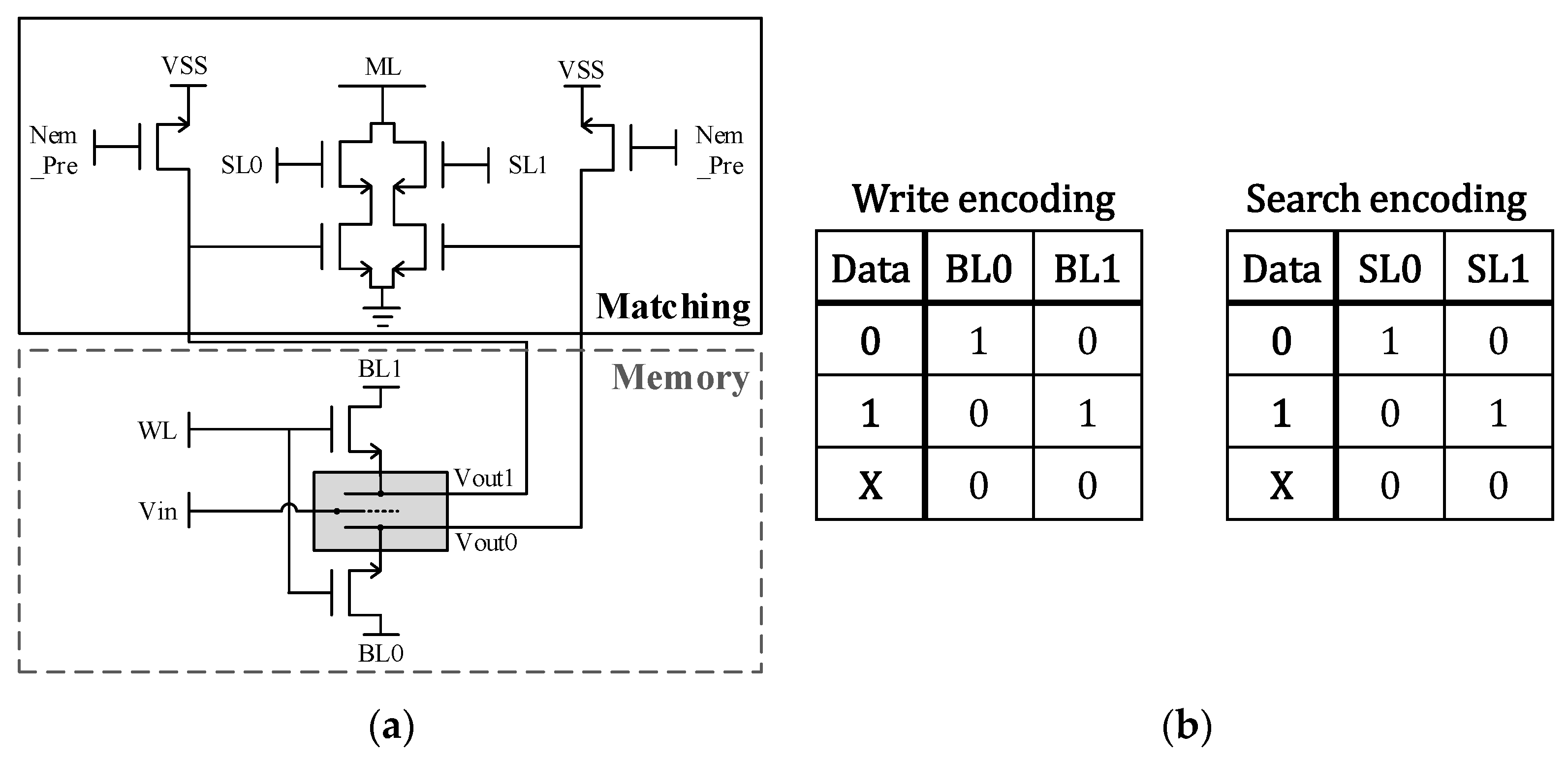
Figure 9a shows a circuit diagram of the NEM-based CAM single-bit cell, and
Figure 9b depicts the data encoding. The basic structure of the NEM-based CAM is the same as that of the SRAM-based CAM. However, there is a major difference between them, in terms of memory and precharge-related circuits.
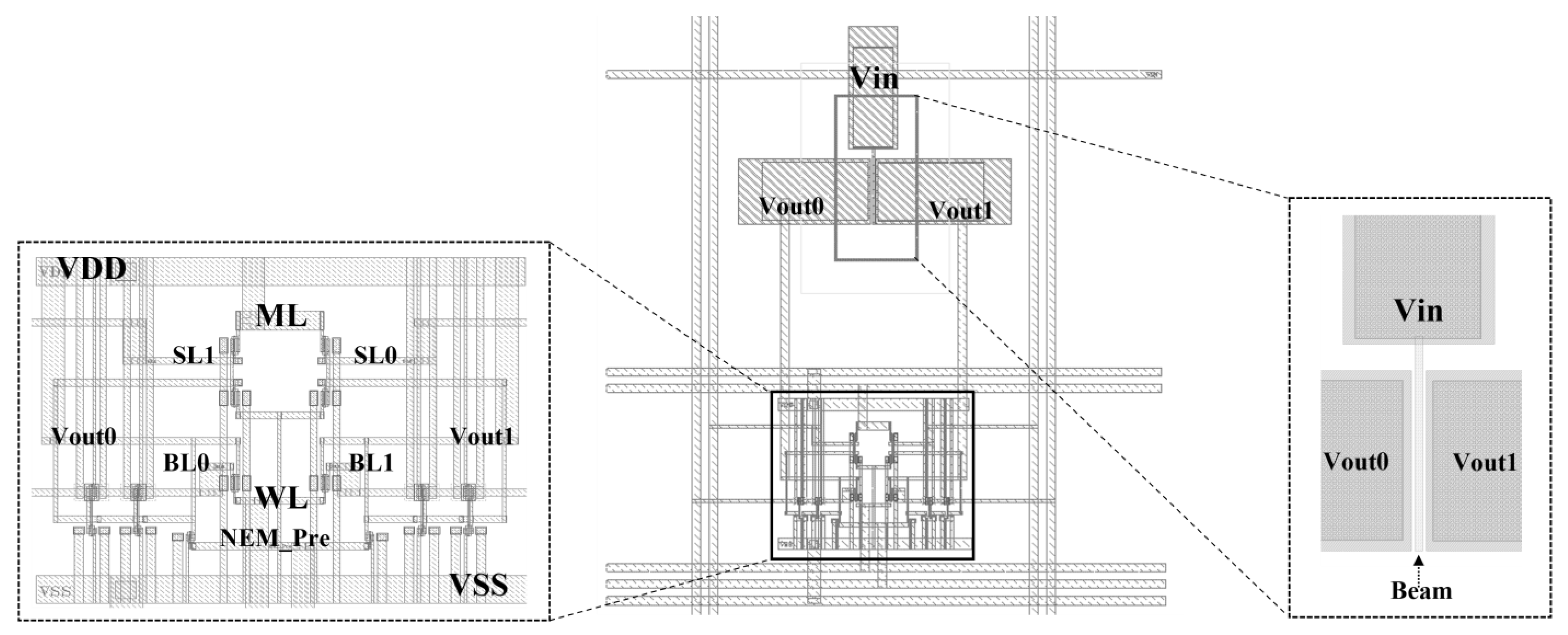
Figure 10 shows the layout of the partial circuit, which is composed of CMOS transistors and responsible for the matching operation in the NEM-based CAM.
Figure 10 also shows the layout of the NEM memory-switch device responsible for the memory in the NEM-based CAM. The CMOS-based CAM uses CMOS transistors for its memory; however, the NEM-based CAM uses the NEM memory switch using the CMOS BEOL process for its memory. Another difference is in the precharge-related circuits. The CMOS-based CAM requires precharge- and enable-related circuits for the BL and SL, whereas the NEM-based CAM can perform the search operation by providing a search signal to the Vin pin without additional circuits.
The basic write and search operations of the NEM-based CAM, utilizing the CMOS BEOL process, are the same as those of the CMOS-based CAM. First, a high value is applied to the WL. Then, a high value is applied to the BL, corresponding to the value to be stored, and the beam of the NEM memory switch is connected to the path to perform the write operation. During the search operation, a high value is applied to the SL, corresponding to the value to be searched for. A high value is applied to Vin, which is delivered to the path connected to the beam of the NEM memory switch. Whether a match exists can be determined by receiving the voltage delivered from Vin and the value of the SL and connecting them to two NMOSs connected in series. Prior to applying a high value to Vin, Vout0 and Vout1 of the NEM memory switch are maintained in a floating state, when operating with only the basic circuits that constitute the CAM. Imperfect operations occur for this reason, and a precharge circuit using NMOS is implemented to solve this problem. The NEM-based CAM single-bit cell does not use separate transistors for its memory cell, and the search operation is carried out using the Vin of the NEM device; hence, transistors are not used. Two additional transistors are used for the write operation, and the upper CAM cell uses four transistors for the match operation. Unlike the CMOS-based CAM, the NEM-based CAM cell does not require a separate precharge circuit; thus, it has the advantage of using fewer transistors.
However, two additional transistors are used for precharge. In total, eight transistors are used in the NEM-based CAM. As the NEM memory switch is on the top metal, it can be laid out vertically in relation to the CMOS transistors. The width of the NEM-based CAM single-bit cell is 20 μm and its height is 12 μm.
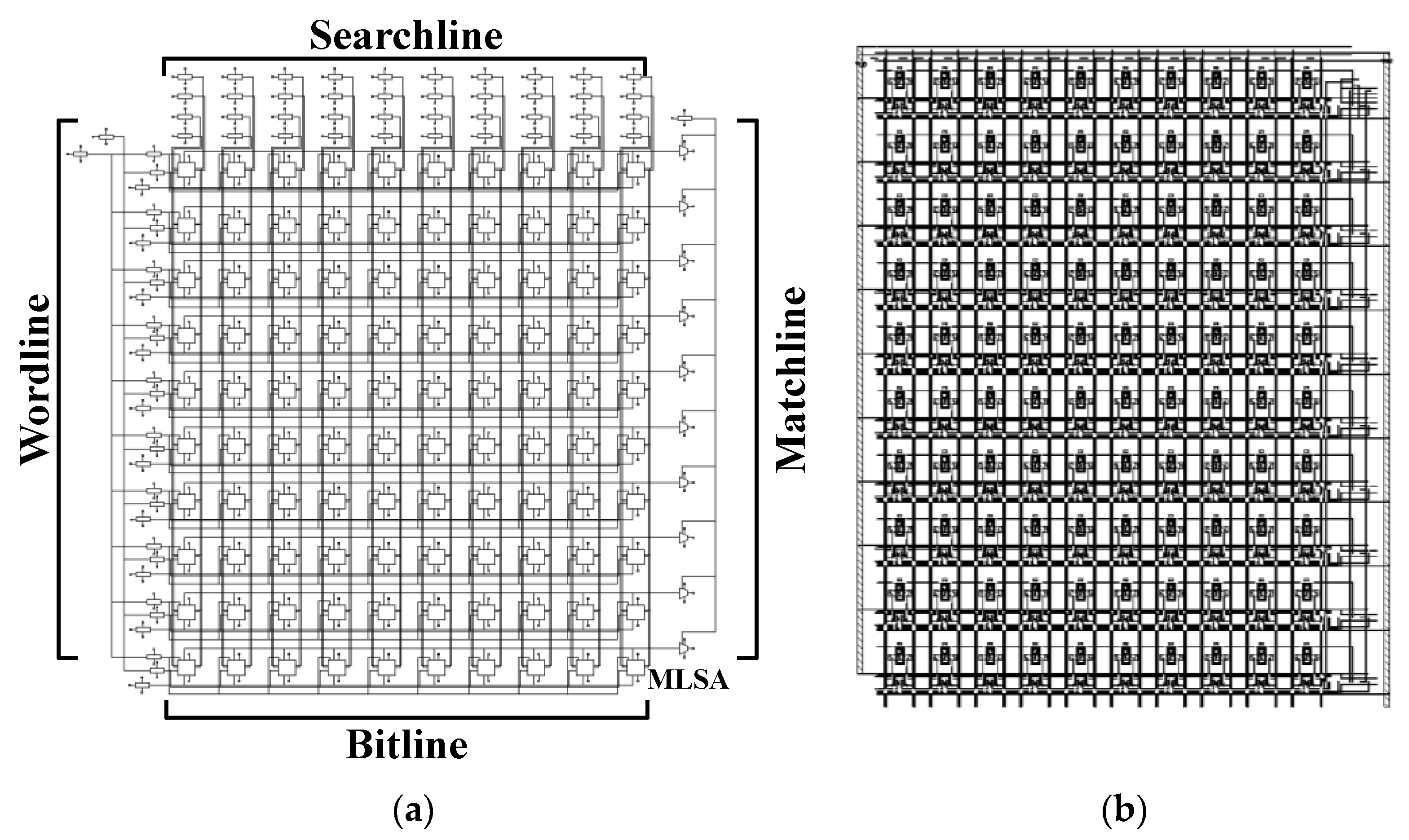
Figure 11a shows the schematic of the NEM-based 10 × 10 CAM array, and
Figure 11b shows the layout. As the NEM memory switch is on the top metal, it can be laid out vertically in relation to the CMOS transistors. The width of the NEM-based CAM single-bit cell is 20 μm and its height is 12 μm.
Figure 11a shows the circuit diagram of the NEM-based 10 × 10 CAM array, and
Figure 11b shows the layout.
4. Simulation
In this study, we used Cadence’s Spectre simulation platform to perform the simulation, and we used Mentor Graphics’ Calibre LVS and DRC verification software to verify the circuit design and layout. Moreover, the Verilog-A model was used for the proposed NEM memory switch [
27].
The single-bit unit cell and 10 × 10 array of the proposed NEM-based CAM were simulated. For a simple comparison, the pre-layout simulation and post-layout simulation were performed for the single-bit cell and the 10 × 10 array of the CMOS-based CAM, and then a final comparison was performed.
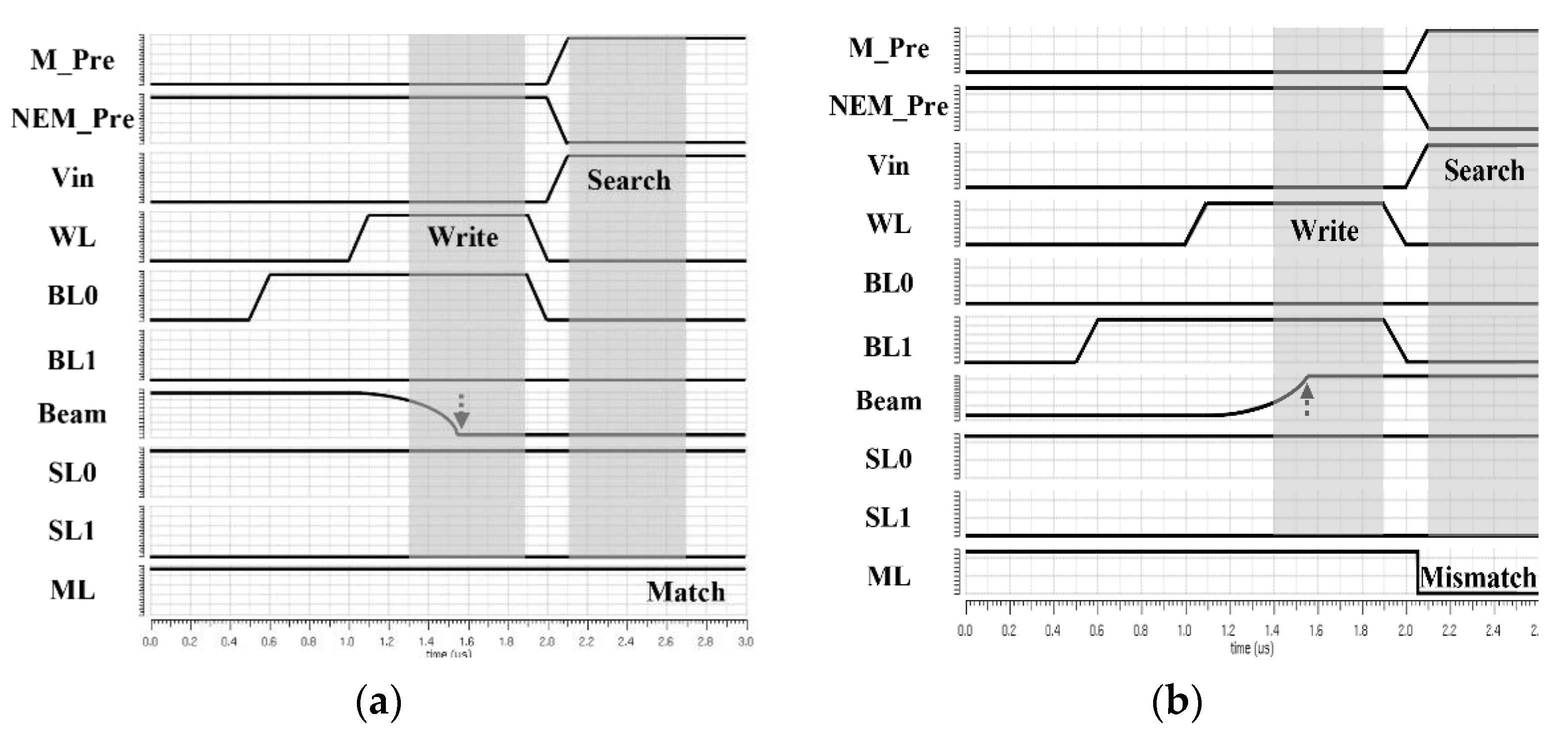
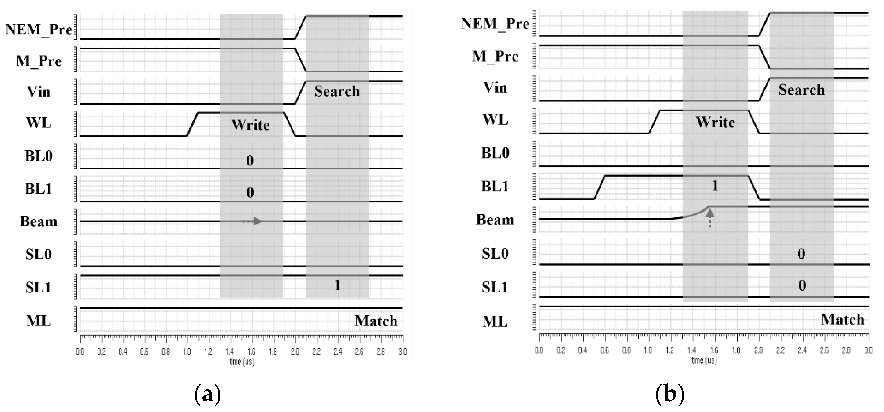
Figure 12 shows the results of the BCAM pre-layout transient simulation, which verified the operation of the NEM-based CAM single-bit cell proposed in this paper. The results for the data match/mismatch in the general data write and search operations were confirmed. It can be seen from the transient simulation that a state transition (initial state to state 1) takes about 0.5 μs during the write operation of a given NEM memory switch. The change in the beam position of the NEM memory switch is shown in the beam row of the transient simulation shown in
Figure 12. However, the NEM memory switch responds faster for the search operation; hence, the operation can be performed in ns time units. In
Figure 12a, a high signal is applied to BL0, and Beam and Vout0 in
Figure 9 are connected to write a ‘0’ to the NEM memory. To prevent Vout0 and Vout1 from staying in the floating state, the NEM precharge signal is kept high during the write duration, which turns on the PMOS circuits to maintain the pull-down path.
Subsequently, a high signal is applied to Vin to perform a search operation, and the ML precharge signal is disconnected, yielding a ‘match’ result in the ML row of the graph. When ‘0’ is written, it can be seen that the beam is connected to the lower path. As the stored bit ‘0’ and the search key ‘0’ match, the ML maintains a high value, indicating a ‘match’. In
Figure 12b, a high signal is applied to BL1, and Beam and Vout1 of
Figure 9 are connected to write a ‘1’ to the NEM memory. The subsequent operation is the same as in the previous description, and the match result is shown in the ML row of the graph. When a ‘1’ is written, it can be seen that Beam is connected to the upper path. As the stored bit ‘1’ and the search key ‘0’ do not match, the ML cannot maintain a high state and is discharged to GND, indicating a ‘mismatch’.
Figure 13 shows the pre-layout transient simulation for verifying the TCAM operation. In
Figure 13a, a low signal is applied to both BL0 and BL1, so Beam in
Figure 9 is not connected to both Vout0 and Vout1. As a result, ‘X’ (don’t care) is written to the NEM memory. The subsequent operation is the same as in the previous description. The ‘match’ result appears in the ML row of the graph. When ‘X’ is written, it can be seen in the Beam row of the graph that Beam is not connected to any path and maintains a floating state.
The stored bit ‘X’ always matches the search key, whether the search key is ‘0’ or ‘1’, and the ML maintains a high state. This represents local masking. In
Figure 13b, a high signal is applied to BL1, so Beam and Vout1 in
Figure 9 are connected to write a ‘1’ to the NEM memory. When a high signal is applied to both SL0 and SL1, the search key indicates ‘X’ (don’t care). The subsequent operation is the same as in the previous description. The match result is shown in the ML row of the graph. When a ‘1’ is written, it can be seen that Beam is connected to the upper path. As the search key is ‘X’, it is always matched, regardless of the stored bit, and ML maintains a high state. This represents global masking [
28].
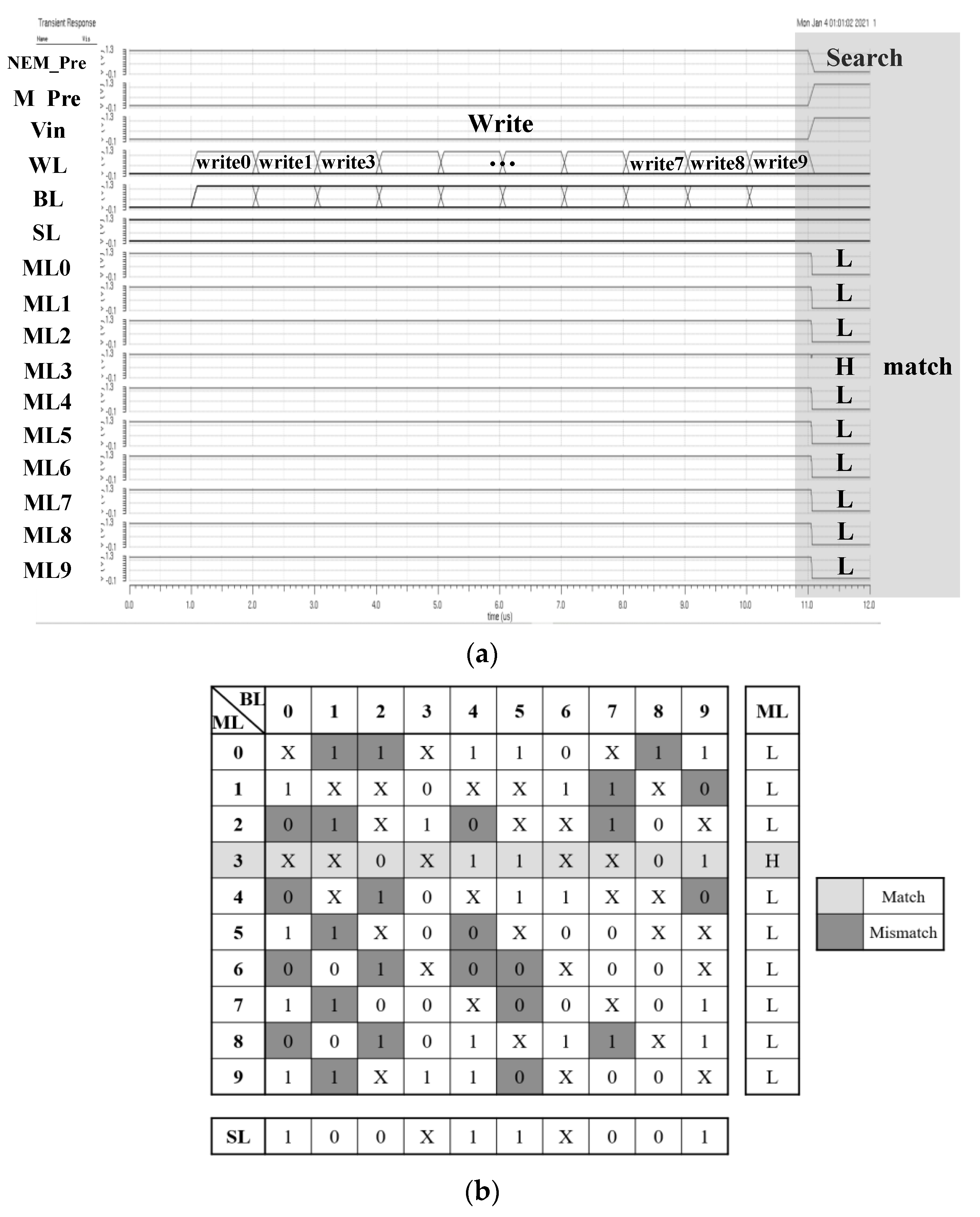
The operation of the proposed CAM 10 × 10 array is verified through the data match/mismatch results from the data write and search operations. When the data match, the ML remains in the precharged-high state. When the data do not match, the ML drains to a low state. The post-layout simulation for the operation verification of the 10 × 10 array of the NEM-based CAM is shown in
Figure 14a. The simulation test bench is shown in
Figure 14b. Each write stage is performed in 1 μs units, and the search stage is performed in 1 ns units. If the BL and the SL match or local/global masking is applied with a value of ‘X’, the ML is in a high state, as shown in row ML3 of
Figure 14a, indicating a ‘match’. On the other hand, if even a single mismatch occurs, the ML is placed in a low state, similar to the remaining ML rows, other than row ML3, indicating a mismatch. The propagation delay and power consumption that occur when a match operation is performed by the single-bit unit cell and the 10 × 10 array of both the conventional CMOS-based CAM and the NEM-based CAM were measured through the pre-layout simulation and the post-layout simulation.
Table 2 shows the comparison of the measurement results for the conventional CMOS-based CAM and the NEM-based CAM. It also shows the improvement rate of the NEM-based CAM proposed in this study, compared to the conventional CAM.
As shown in
Table 2, the proposed NEM-based CAM is able to reduce the propagation delay by about 8% for the single-bit cell and 23% for the 10 × 10 array, compared to the CMOS-based CAM in the layout simulation. In addition, the power consumption during a match operation is reduced by up to 2.6 times for the single-bit cell and 3.0 times for the 10 × 10 array by the proposed NEM-based CAM. It is worth noting that the improvement in delay and power is enlarged as the array of CAM becomes larger.
The number of transistors used in the circuit design and the area of the actual design layout were compared with those of the single-bit unit cell of the conventional CMOS-based CAMs and the single-bit unit cell of the NEM-based CAM.
Table 3 shows the number of transistors used in the CMOS-based CAMs and the NEM-based CAM, a comparison of the area of the front-end areas, and the improvement rate of the proposed NEM-based CAM, compared to the conventional CAMs.
According to the experimental results, the number of transistors used in the circuit constituting the proposed NEM-based CAM was reduced by about 2.6 times, compared to the CMOS-based BCAM, and by about 5.8 times, compared to the TCAM. Moreover, because the NEM memory switch can be laid out vertically, the polysilicon substrate area can be saved. Hence, the area of the front-end area of the proposed NEM-based CAM was reduced by about 71.9%, compared to the CMOS-based BCAM, and by about 89.3%, compared to the TCAM. As shown in
Table 2 and
Table 3, the advantages of NEM-based CAM are expected to be expanded when a larger size than the size presented in this study is designed.
5. Measurements
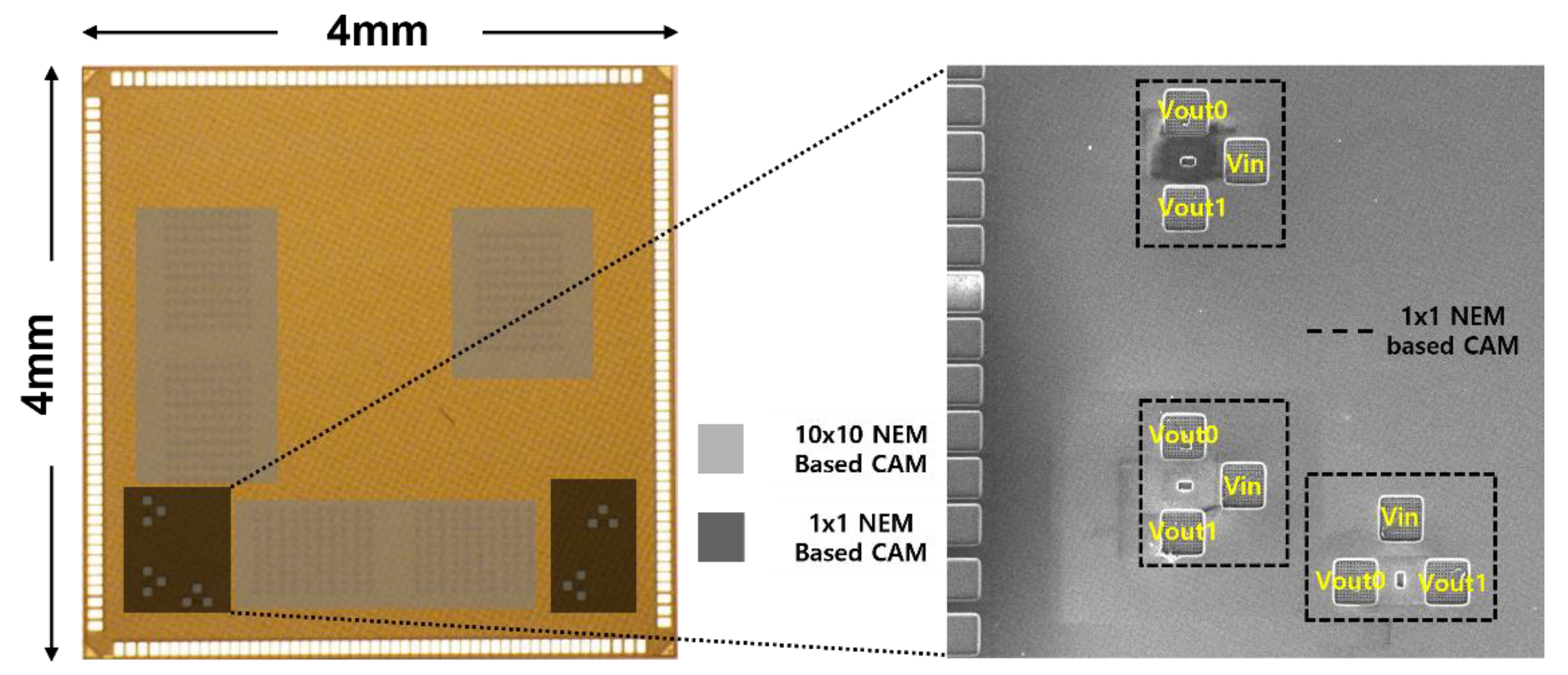
In this study, the 65 nm CMOS process was used to design and fabricate a chip.
Figure 15 shows a die photo of the fabricated chip. The NEM-based CAM memory array was designed in sizes of 10 × 10 and 1 × 1. The 1 × 1 NEM-based CAM memory unit was fabricated to examine whether the movable beam transitioned properly from the initial floating state to the V
L1 or V
L2 state. In addition, pads corresponding to Vout0, Vout1, and Vin were added to the 1 × 1 NEM-based CAM, in addition to the pads that exist on the outer area of the chip. We used a probe station to measure and verify the normal operation of the movable beam.
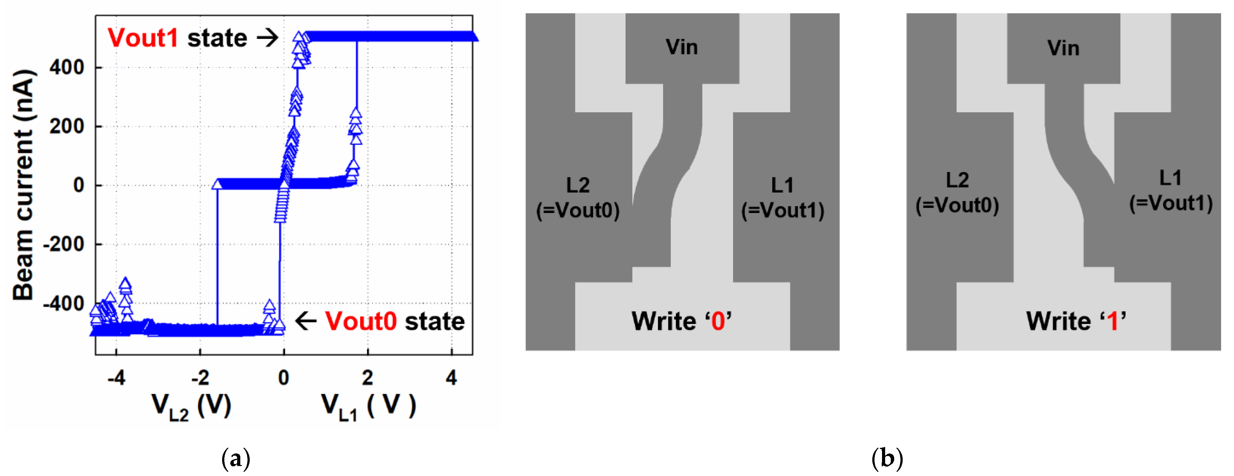
Figure 16a shows the switching behavior of V
L2 state (Vin = Vout0) and V
L1 state (Vin = Vout1) of a NEM memory switch. Possible micro-welding effects in NEM memory switches are suppressed by limiting the maximum current level to 500 nA during measurement [
26]. To check whether the movable beam can be in contact with the two states normally, an experiment was conducted with the additional PAD mentioned above. A total of 10 times were toggled by applying voltage to the PAD corresponding to Vout0 and Vout1, respectively, and it appears that a path was formed normally, as shown in
Figure 16b, and the NEM memory switch repeated the transition between the V
L1 and V
L2 states in a non-volatile manner within 1.2 V. Considering that the NEM memory switch may corrode when it is continuously exposed to room temperature, owing to its characteristics, a chip on board (COB) was made for measurement, after connecting the movable beam to the Vout1 (‘1′) state.
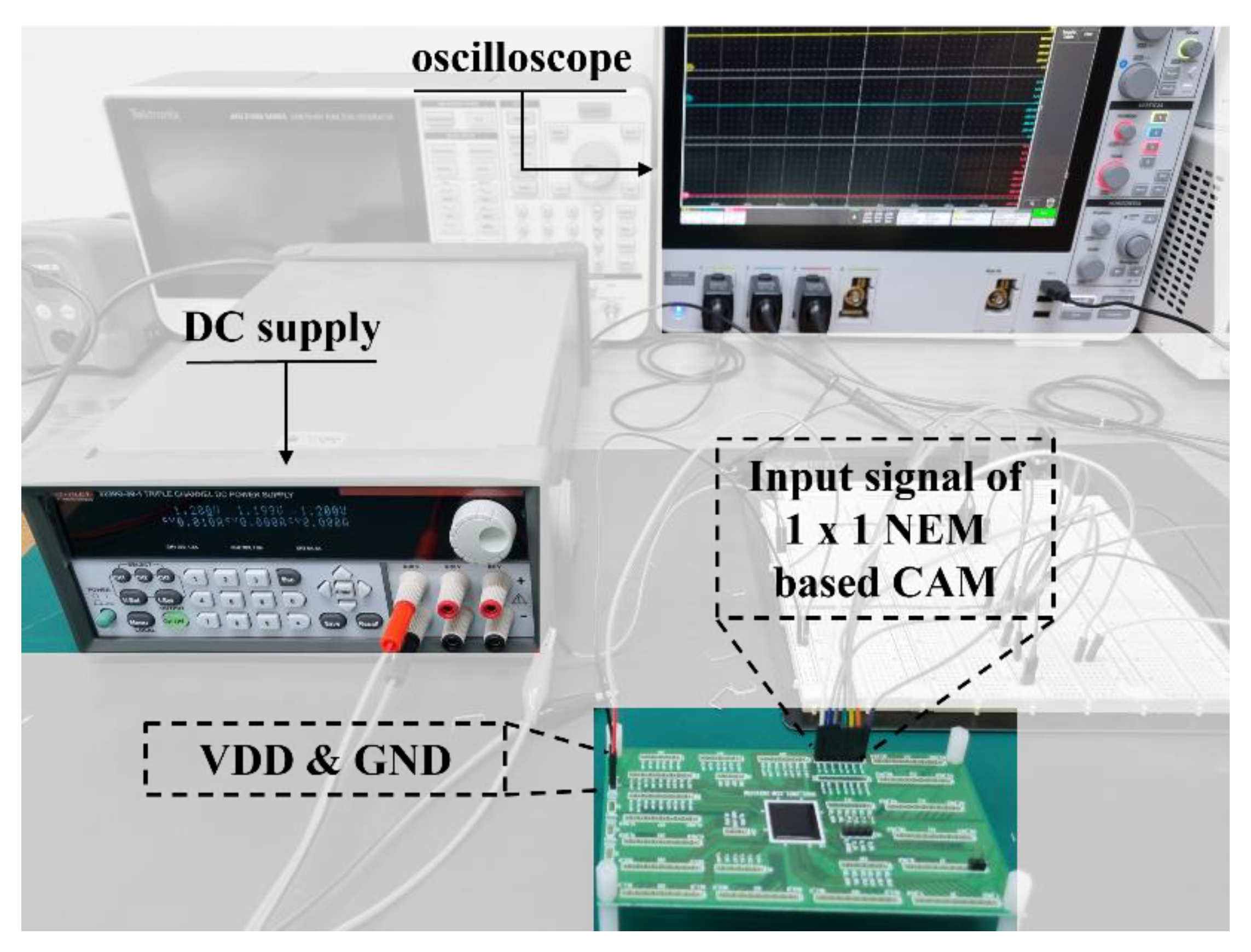
As shown in
Figure 17, the experimental equipment was set up to check the 1 × 1 NEM memory-switch-based CAM, based on the COB. VDD and GND were controlled through the DC power supply, and the waveforms of Vin and the ML were verified using an oscilloscope.
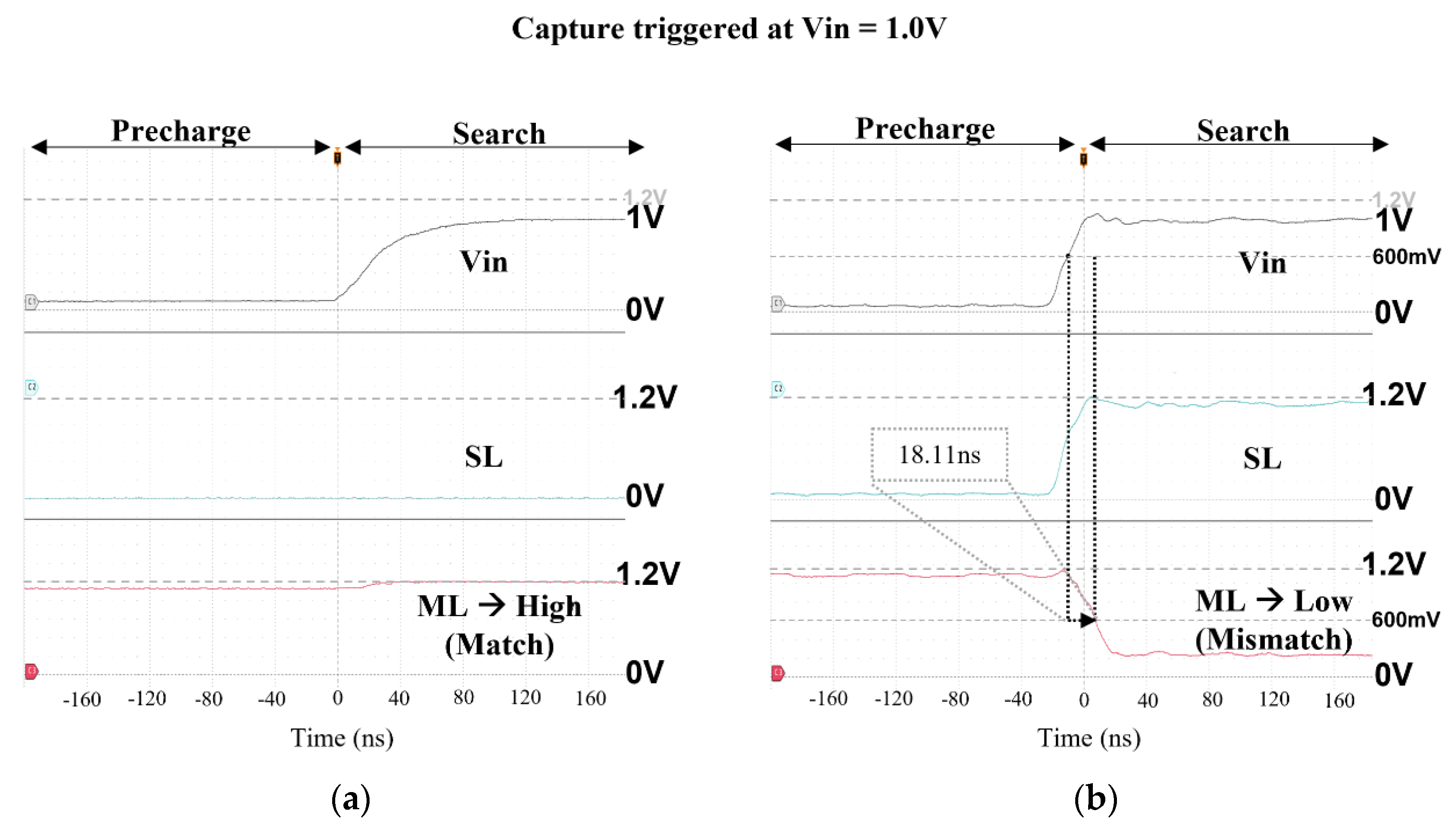
The match and mismatch operations were verified assuming data ‘0’ was stored, as shown in
Figure 12a. The Vin signal keeps the ML in a high state through the precharge, and it flows along the movable beam to turn the comparison transistors on or off. First, in the case of a match, a ‘0’ signal is applied to the SL. The ML maintains a high value, which indicates a match, as shown in
Figure 18a.
Conversely, in the case of a mismatch, the search operation was started at the same time a ‘1’ was applied to the SL. While the ML maintains a high state, a pull-down path is formed, owing to the grounding of the NEM-based CAM cell. As a result, a low value is output, indicating a mismatch, as shown in
Figure 18b. We confirmed that the operation results of the fabricated chip are the same as those of the simulation, thereby demonstrating that the NEM memory-switch-based CAM can be applied in practice.


 and
and 


