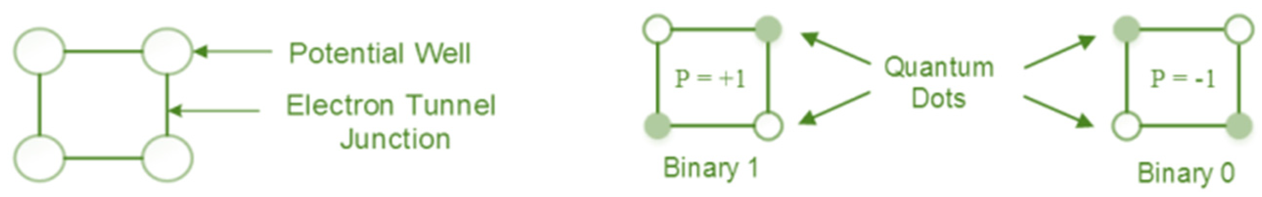
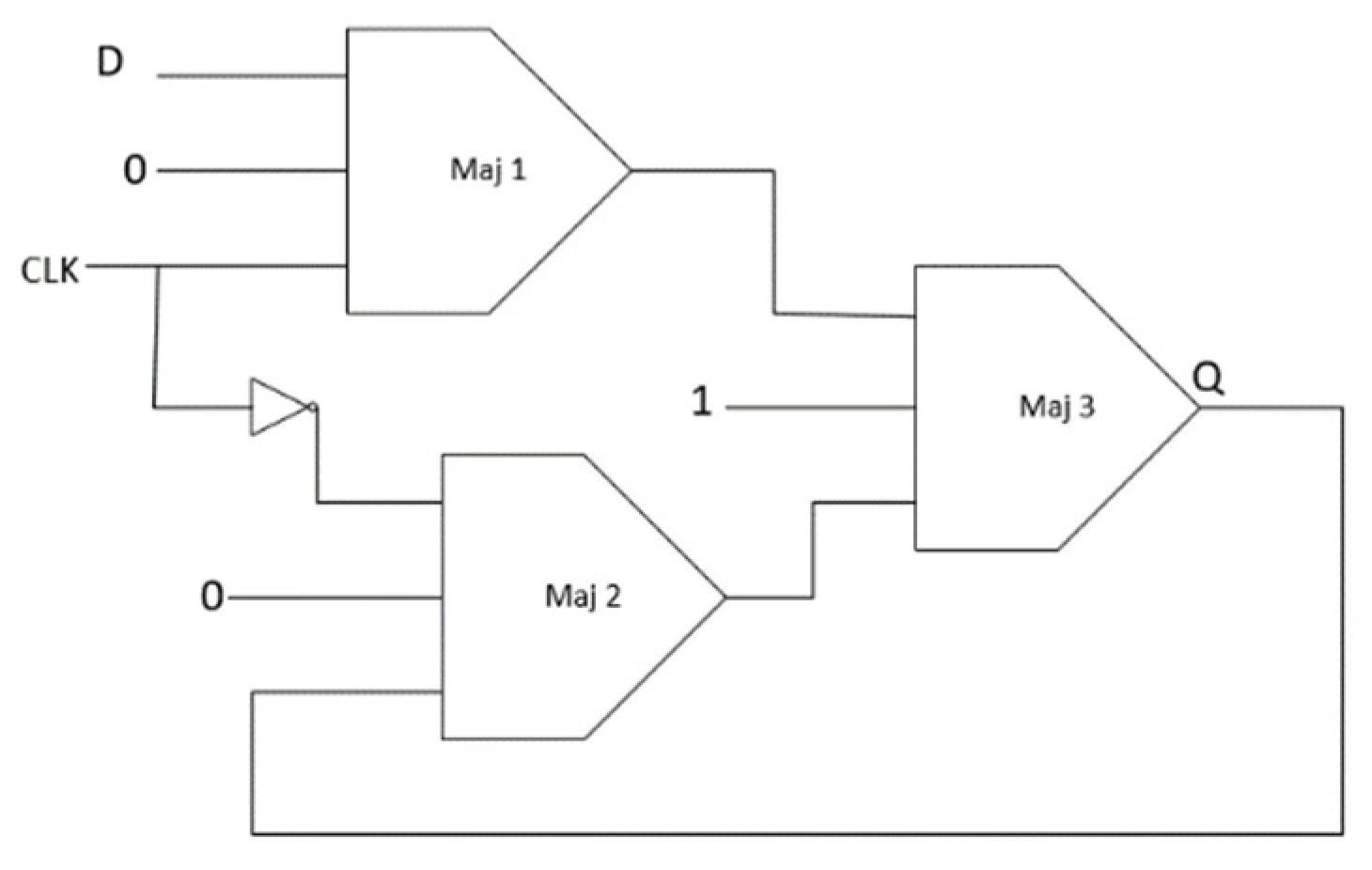
Flip flops and registers form the essential constituent. Many of the digital circuits include special purpose processors and the design of memory chips. DFF and shift registers can further be used for designing counters. In this work, new designs for different types of registers using the proposed DFF were proposed.
4.1. PIPO Designs
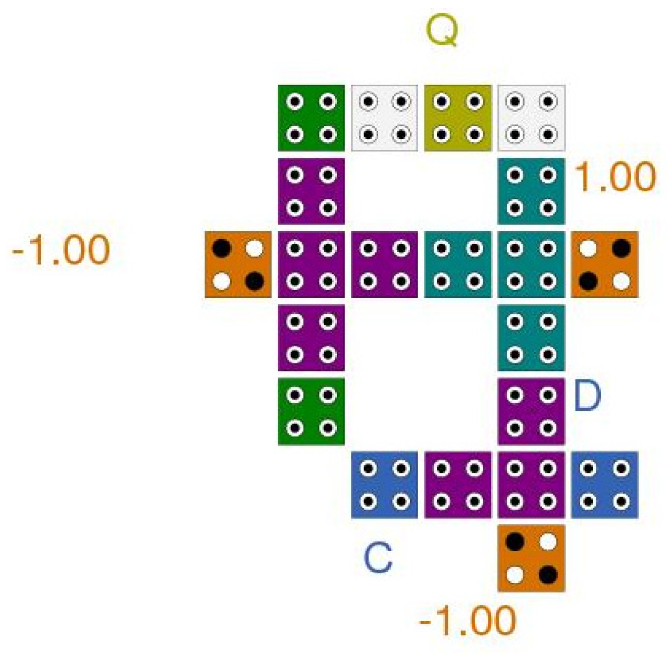
When the inputs are applied in a parallel manner to the register and outputs are obtained in a parallel manner, the register is called a parallel-input-parallel-output shift register. The block diagram of a simple two-bit PIPO formed using three D flip flops is shown in
Figure 10. It can be seen that all inputs enter the respective flip flops in a parallel manner and that all the outputs are obtained parallel too.
The two-bit PIPO shift register was constructed using two proposed DFFs. The proposed DFF design was used here. It utilized 55 cells in its QCA design. The two parallel inputs were
D1 and
D2 for stage 1 and stage 2, respectively.
CLK is the clock signal applied to the circuit.
Q1 and
Q2 were two parallel outputs from stages 1 and 2, respectively. Each stage had a latency of 1 because the QCA clock zone changes four phases from respective input to output with a delay of 0.25 for each zone.
Figure 11 shows the two-bit PIPO shift register design as employed in QCA, and
Figure 12 shows its simulation graph. It can be seen that when the positive level of the clock appears, the outputs start to follow their respective inputs with a delay of 1 for each stage. For the first clock, the input
D1 is 0011, and it can be seen that output
Q1 reflects the same sequence 01 with the delay. The second input
D2 is 0101 for this duration, and output
Q2 reflects the same sequence with the delay of 1.
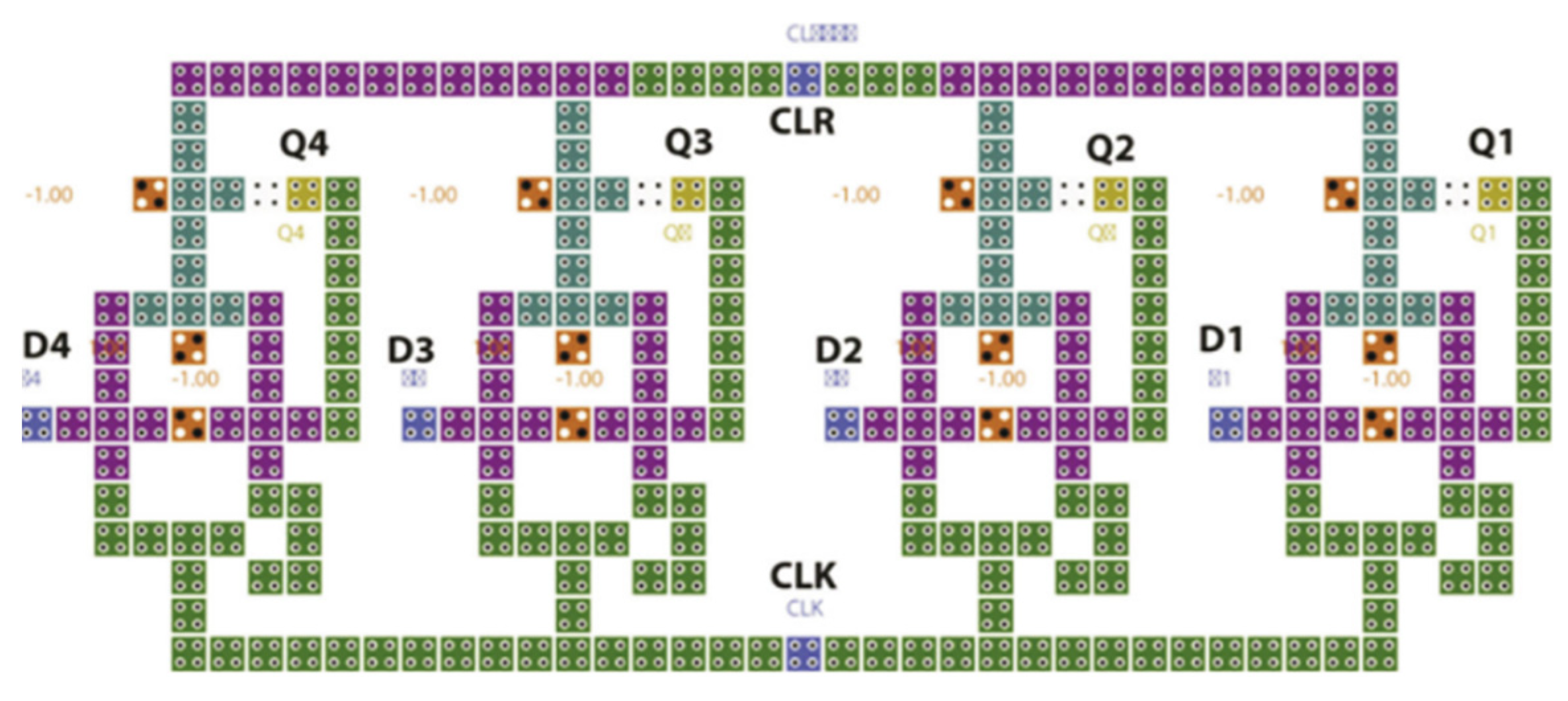
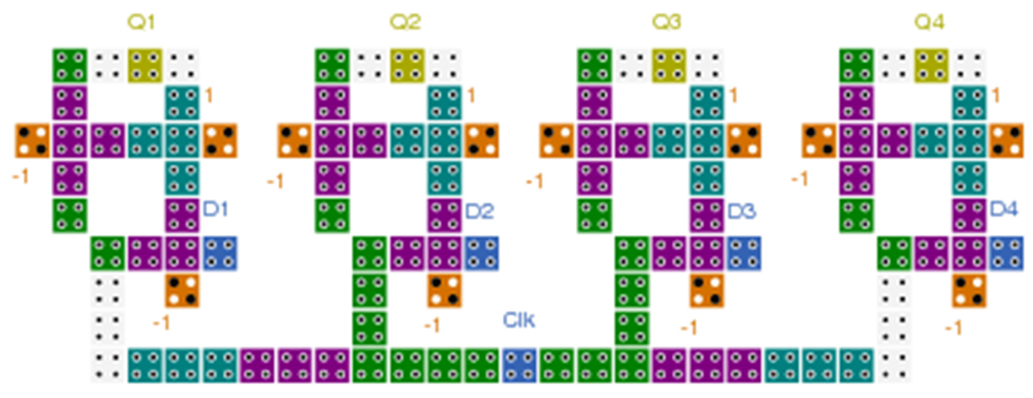
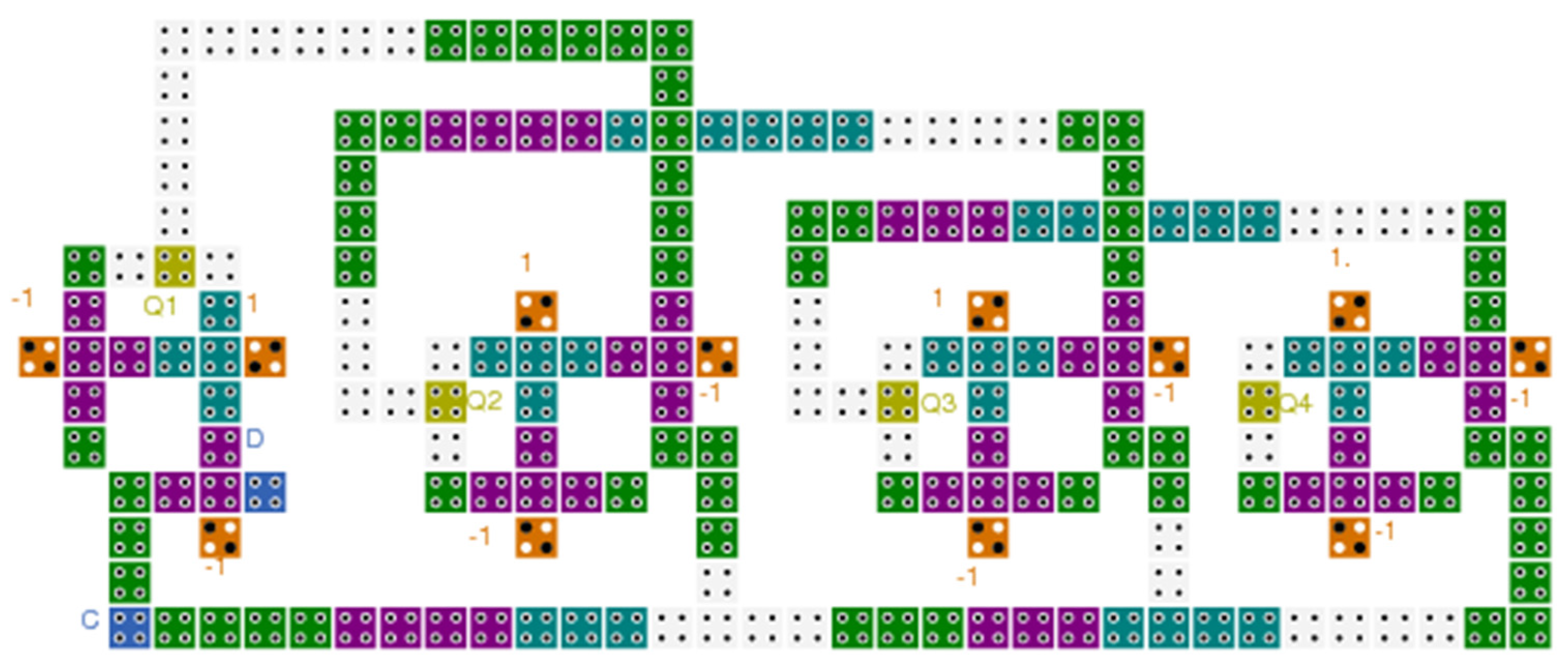
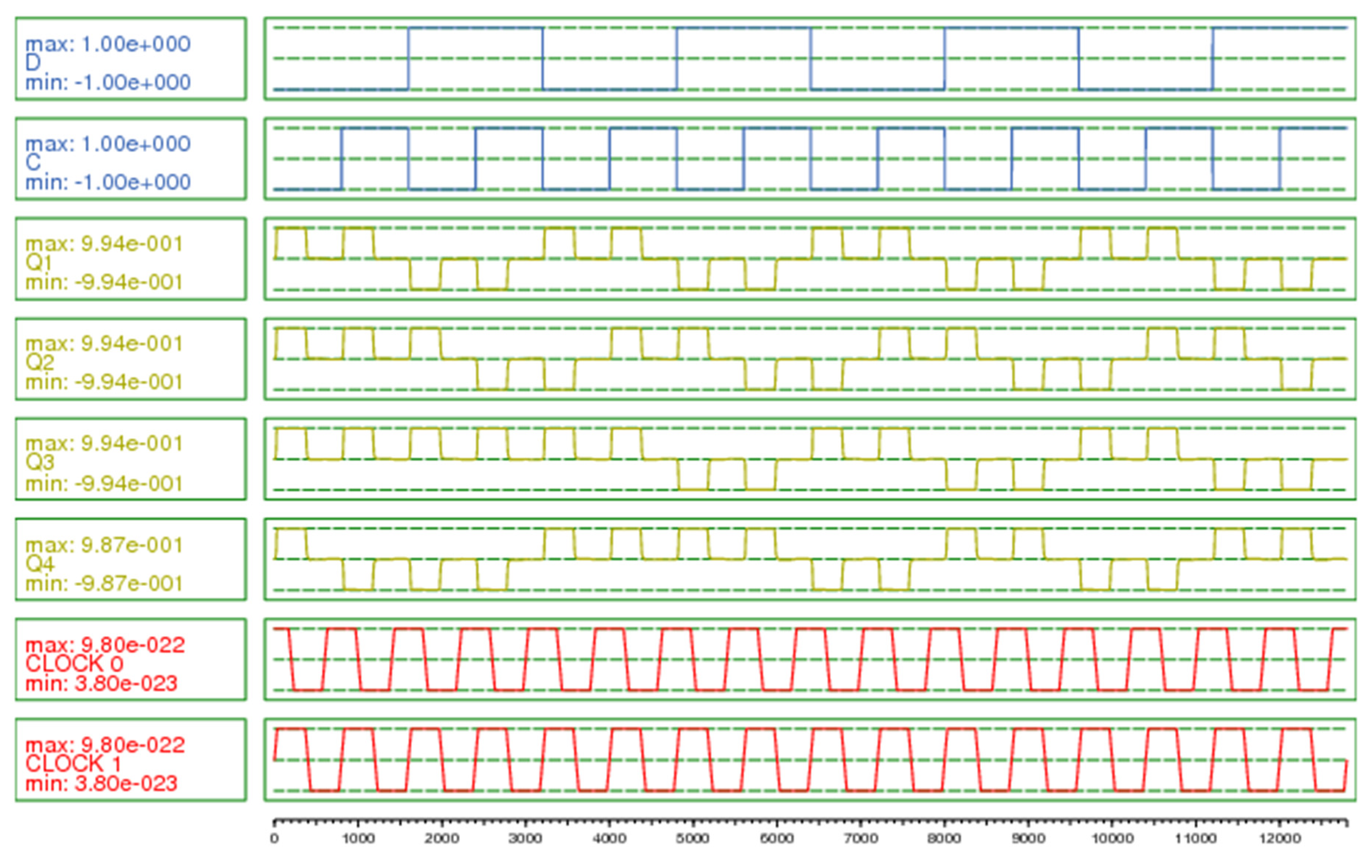
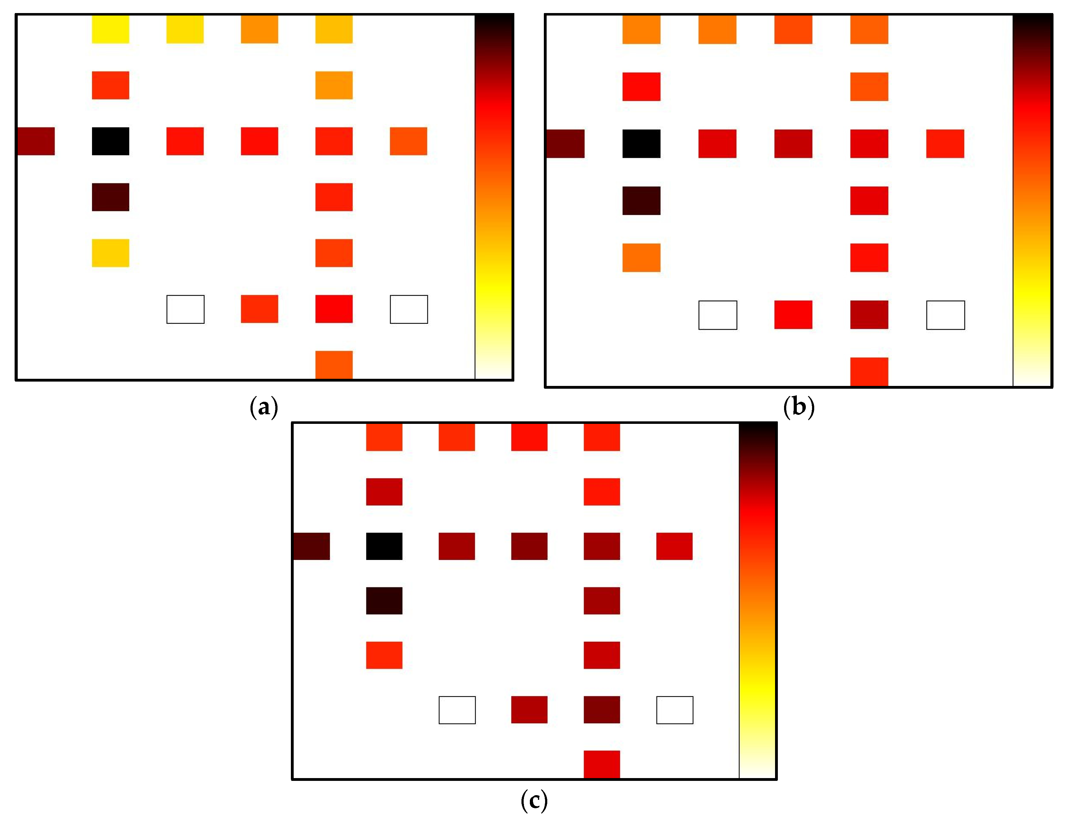
The four-bit PIPO shift register is devised with the use of four proposed DFF. It utilizes 114 cells in its QCA implementation. The four parallel inputs to the four stages are
D1,
D2,
D3, and
D4.
Q1,
Q2,
Q3, and
Q4 are the respective parallel outputs from each of these stages. The latency for each stage is 1.
Figure 13 and
Figure 14 show the four-bit PIPO shift register design as employed in QCA and its simulation graph, respectively.
The performance parameters of the proposed two-bit PIPO and four-bit PIPO shift registers are given in
Table 1. The PIPO designs are effectual in terms of fewer total cells utilized in the design, the area occupied by the cells, total area, cost, and latency.
4.2. SIPO Designs
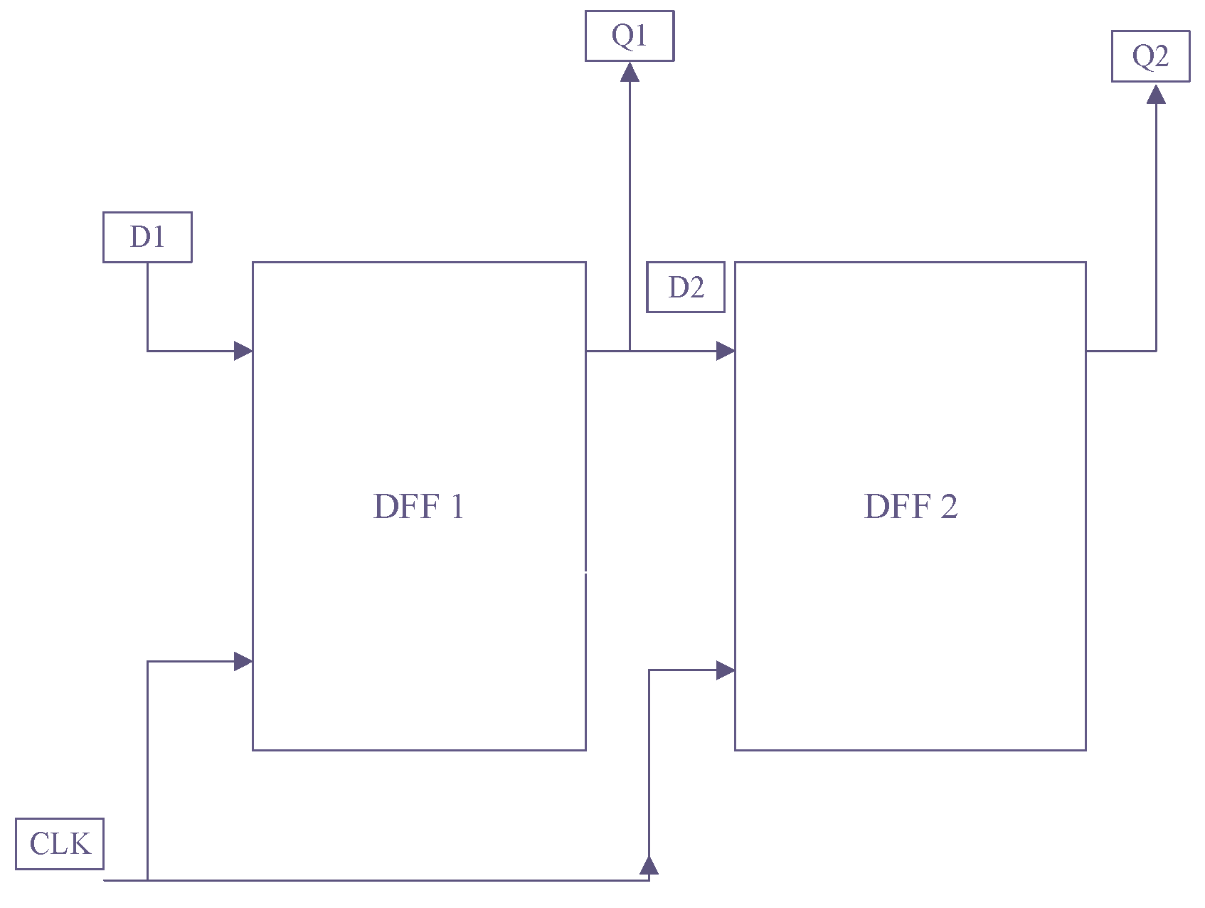
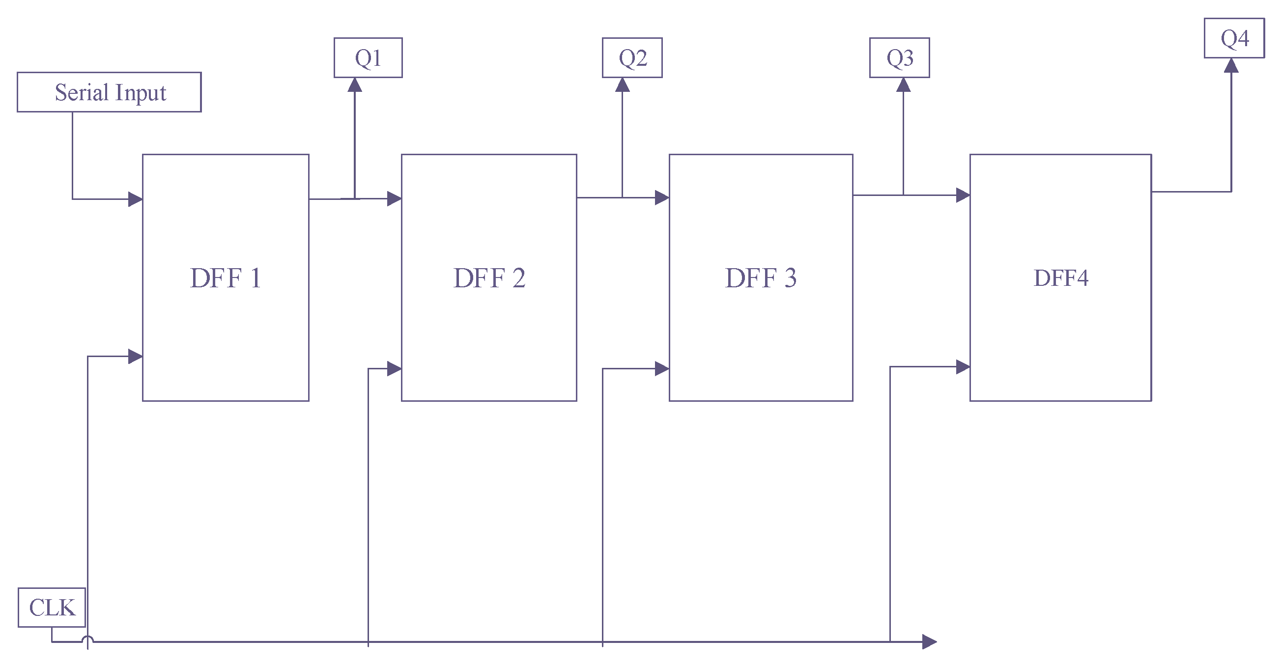
When the input is applied serially and the output is obtained in a parallel manner, the shift register is termed as serial-input-parallel-output.
Figure 15 is the block diagram representation of a four-bit SIPO shift register. It can be seen that all the DFF are joined in a cascade manner where serial input is entered to the first DFF at the left and then the output of one connects to the input of the DFF following it. Since the same
CLK pulse is applied to each of the DFF, the design is synchronous, and the output of each DFF is occupied in a parallel manner.
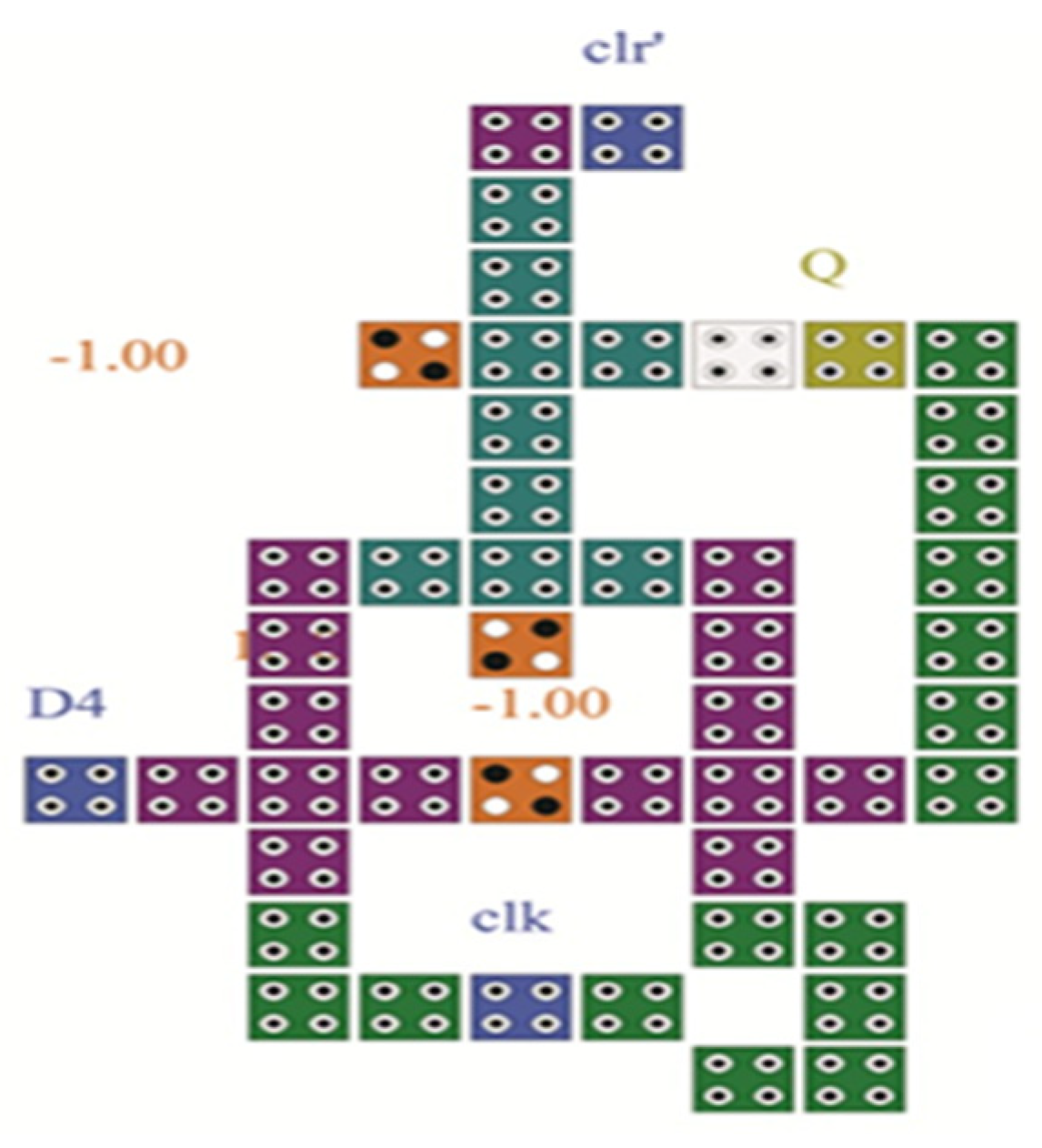
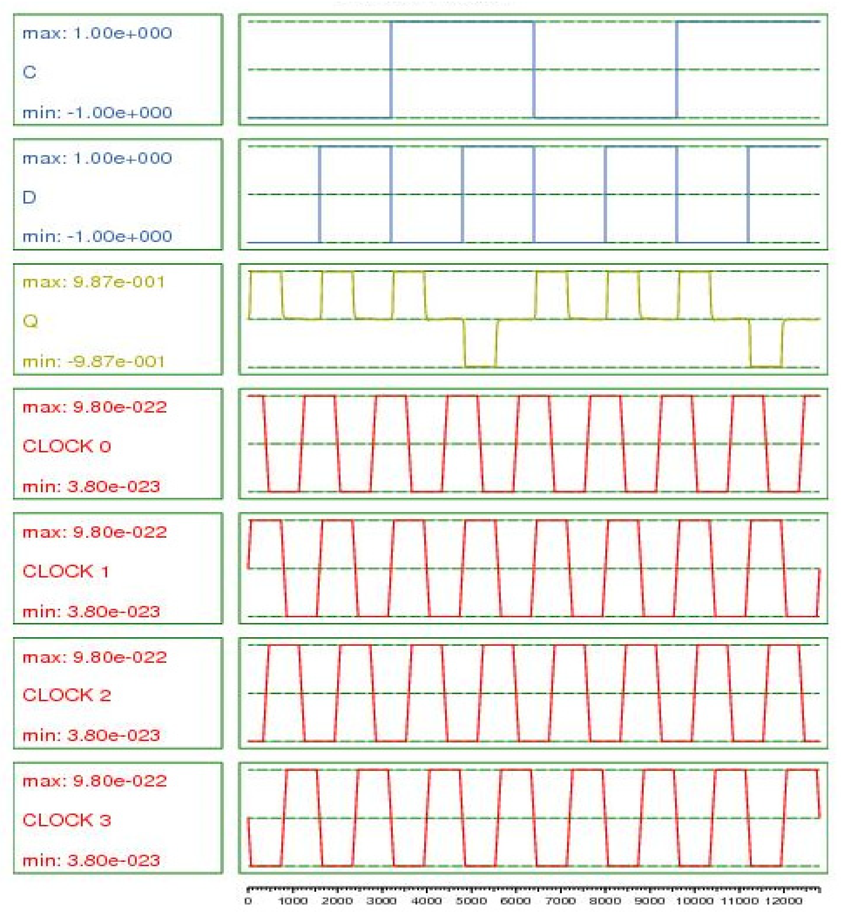
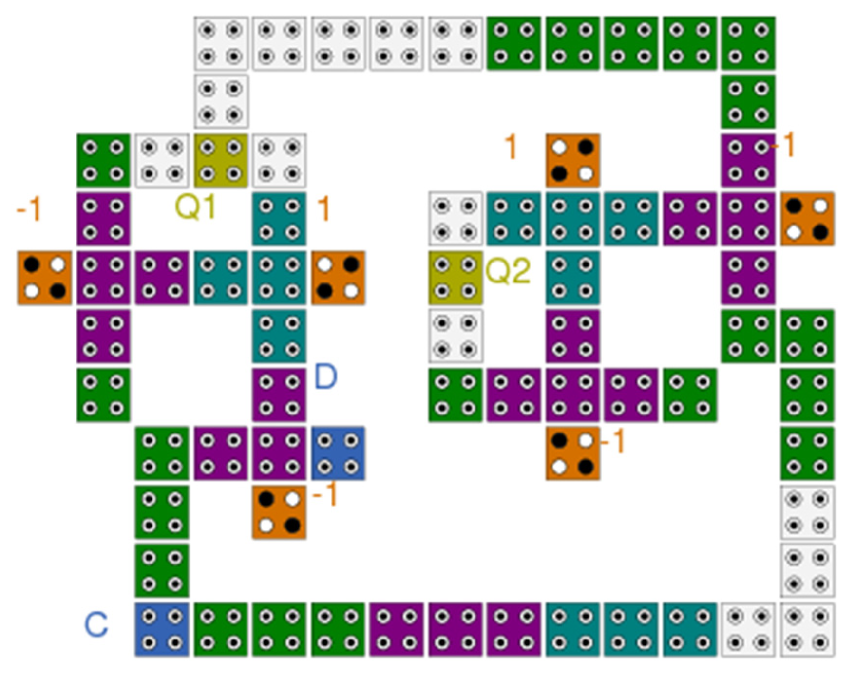
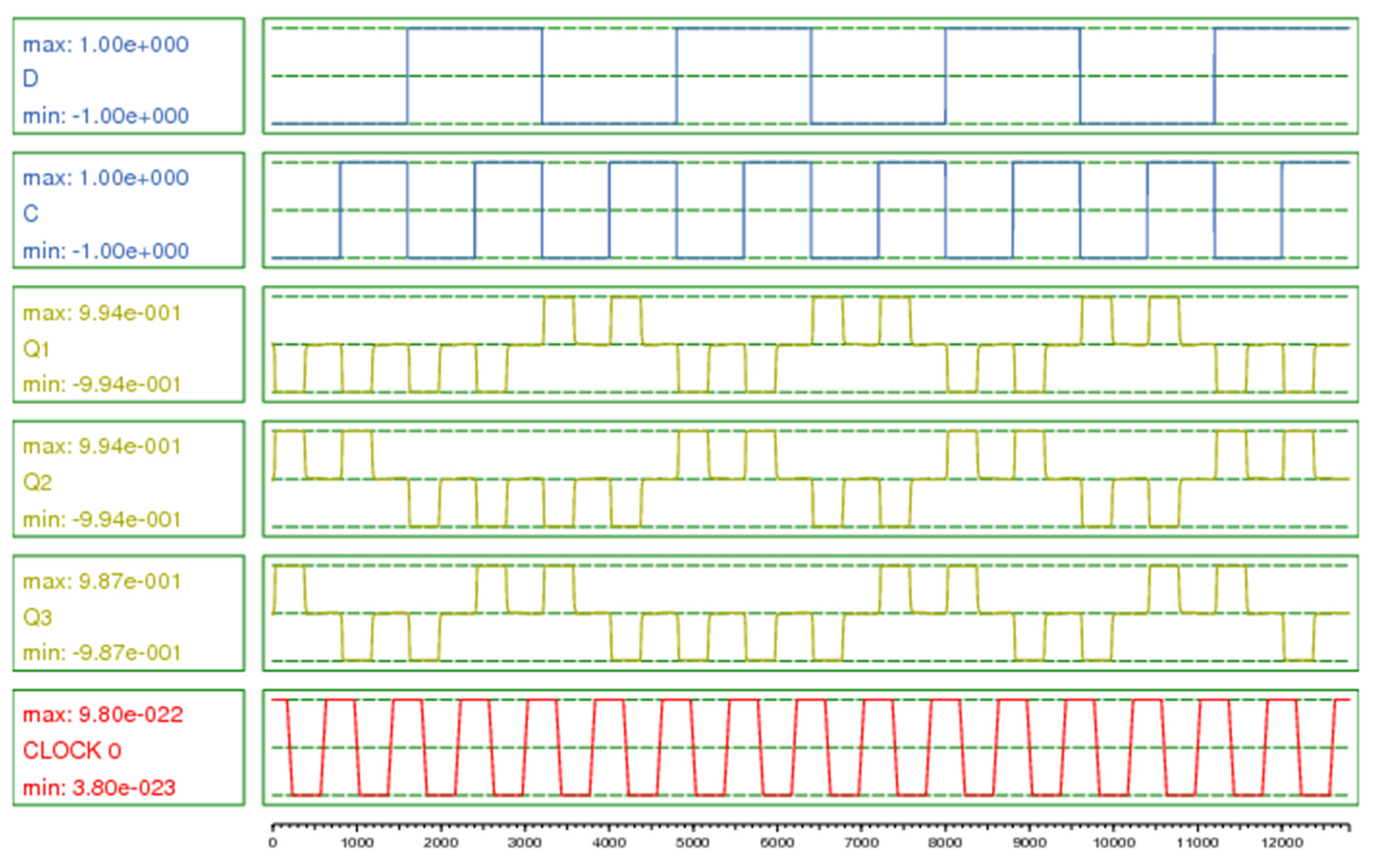
The two-bit SIPO shift register is designed with the proposed design of DFF. It utilizes 73 cells in its QCA design.
D is the serial input applied to the flip flop of the first stage.
Q1 is the first stage output, which connects to the input of the second stage of the SIPO shift register.
Q2 is the stage 2 output. The latency for stage 1 is 1 as the QCA clock zone undergoes four changes from input
D to output
Q1. These changes are clock 1 shown in magenta to clock 2 shown in blue and to clock 3 shown in white. The clock zone undergoes 4 changes from
Q1 to output
Q2, making a total of 8 changes in clock zones from serial input
D to output
Q2 with each change giving rise to a delay of 0.25. Therefore, the delay for the second stage is 2.
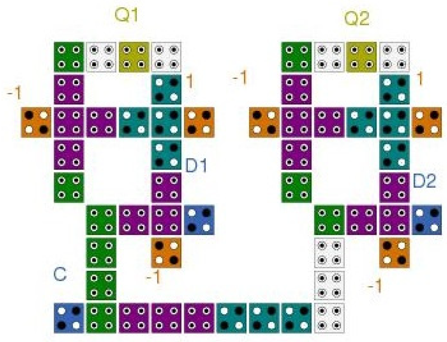
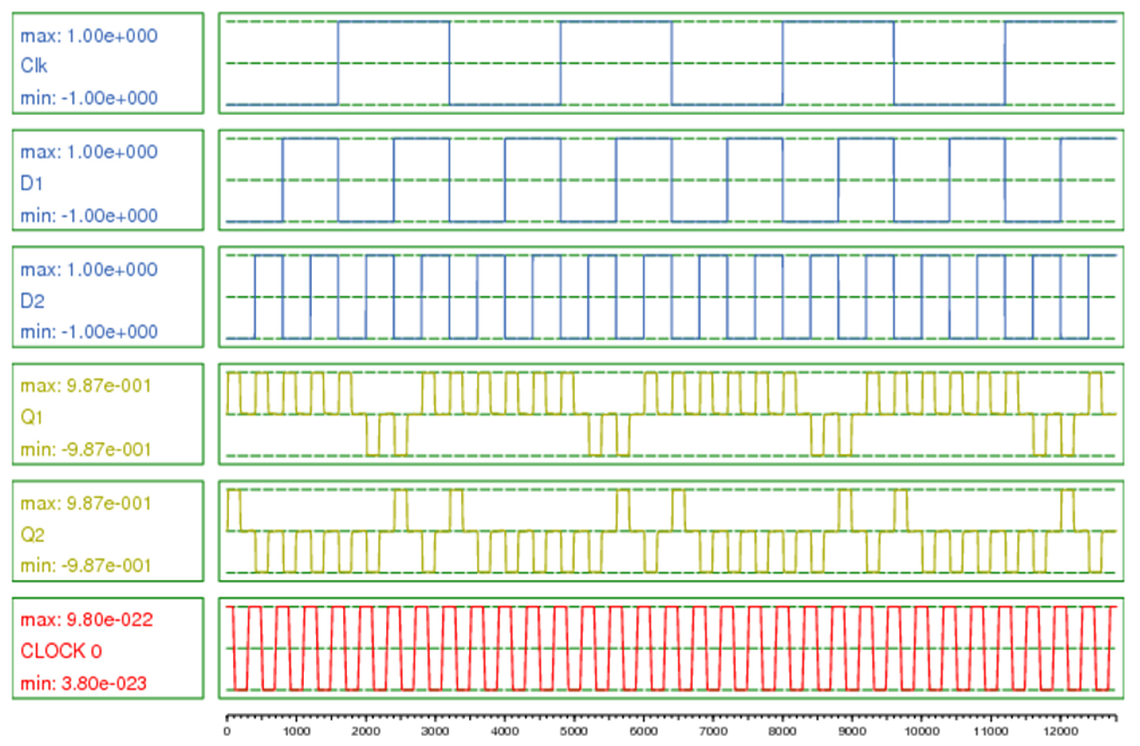
Figure 16 is the implementation of the two-bit SIPO shift register in QCA, and
Figure 17 shows the simulation graph for this shift register. When the first clock pulse appears,
D is 0; therefore,
Q1 follows the serial input and remains 0 until the next clock pulse appears. It can be seen from the simulation graph that output appears after a delay of 1 in
Q1. Then, at the second clock pulse,
Q2 follows the input going to it through
Q1, i.e., becomes 0 with the delay of 2, and at the same time
Q1 goes from 0 to 1 because serial input
D is 1 and has the same value until the next clock pulse appears. This process continues, and the input sequence of 0101 appears at the parallel outputs as it keeps shifting with each clock pulse.
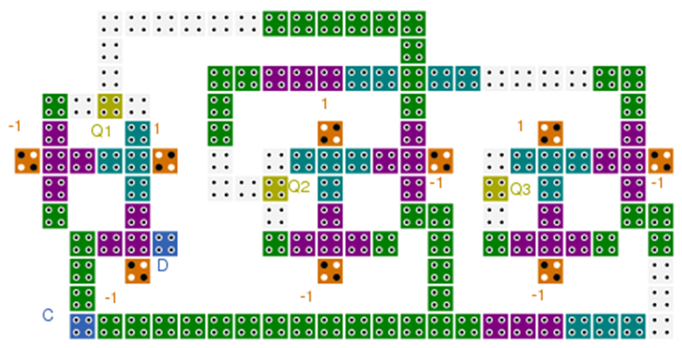
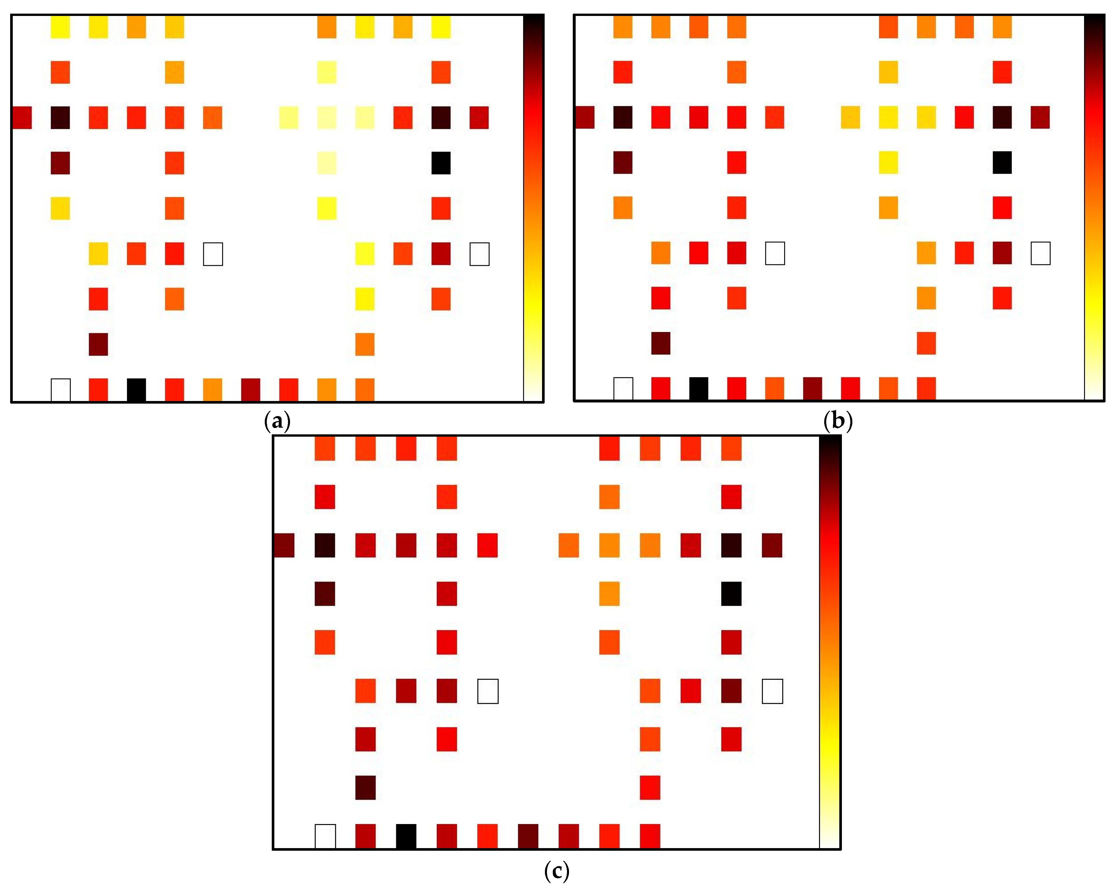
The three-bit SIPO shift register is designed with three proposed DFF forming three stages. It utilizes 133 cells in its QCA design. The latency is 1, 2, and 4 for stage 1, stage 2, and stage 3, respectively. Serial input
D is coupled to the input of the first stage.
Q1,
Q2, and
Q3 are parallel outputs.
Q1 is connected to the second stage input, and
Q2 is connected to the third stage input.
Figure 18 is the three-bit SIPO shift register design as implemented in QCA followed by its simulation graph in
Figure 19.
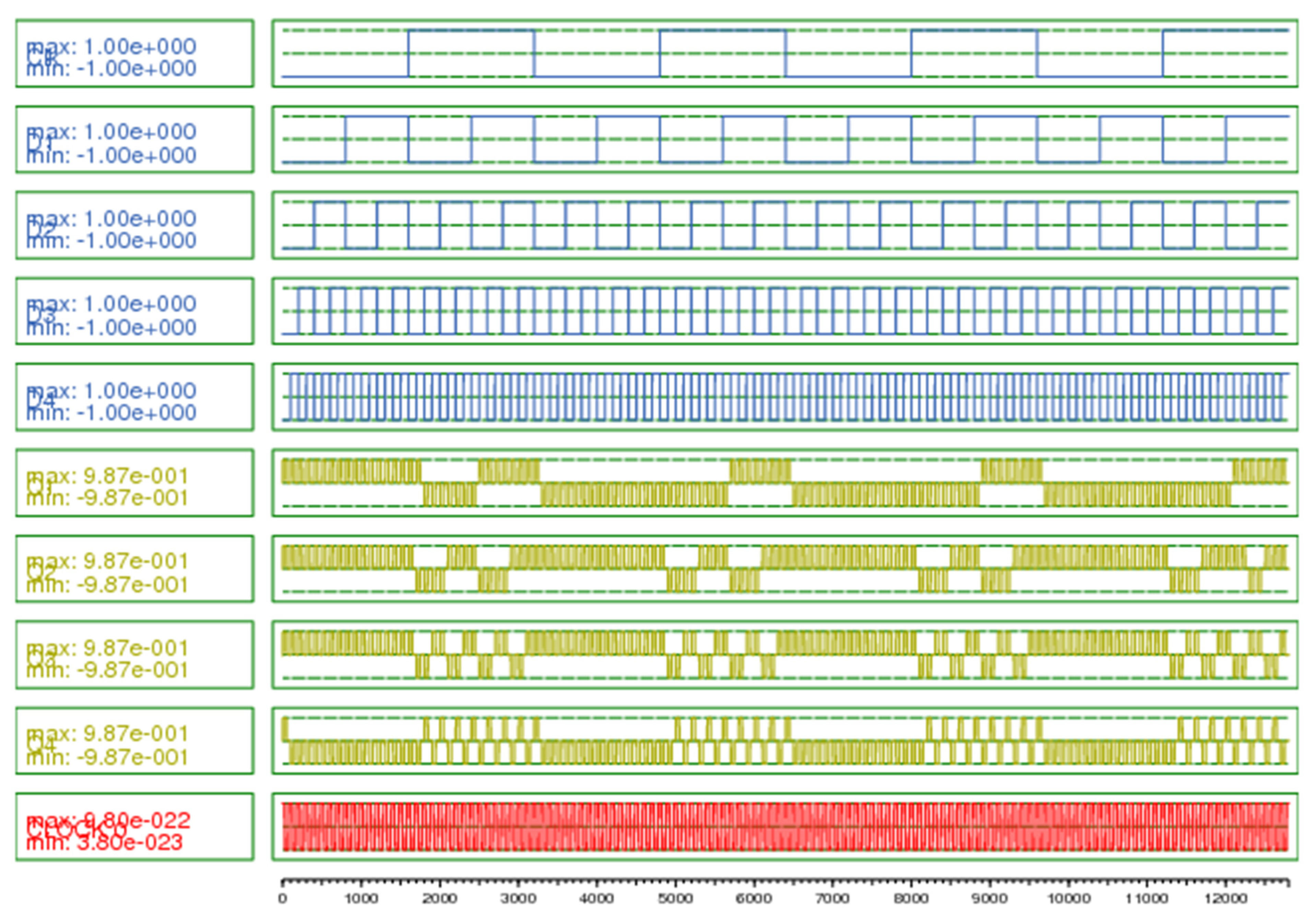
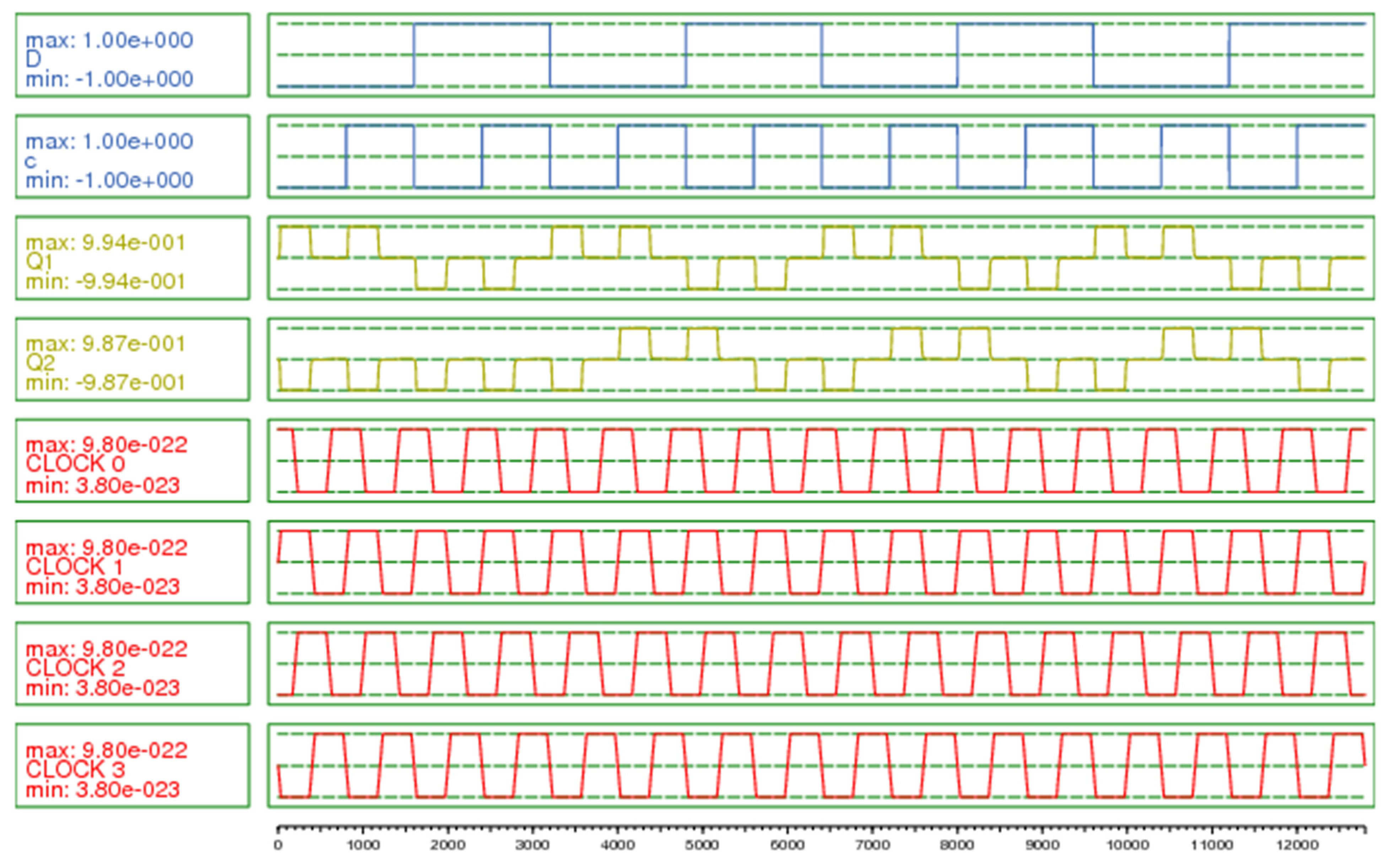
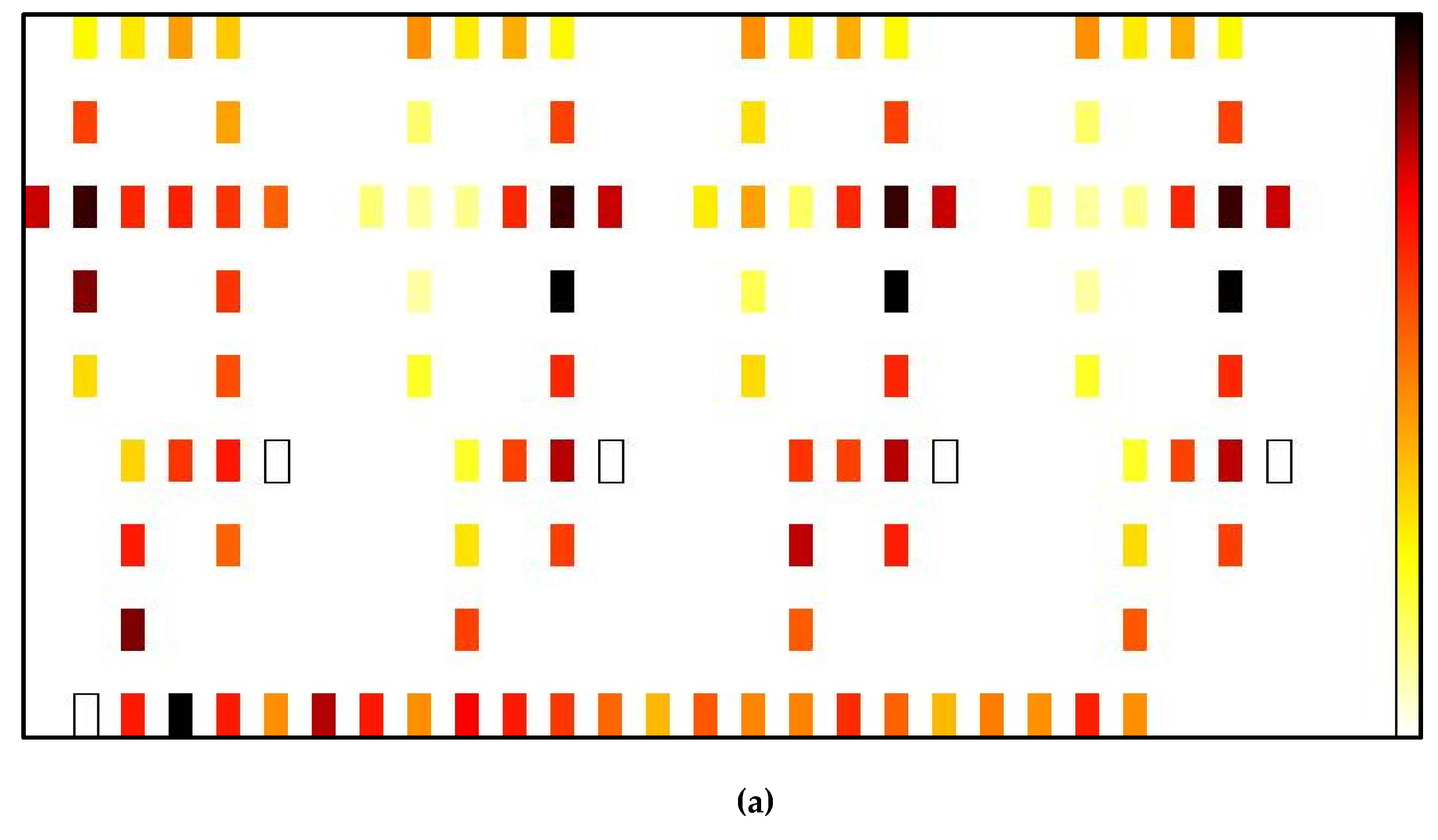
Figure 20 shows the QCA implementation of four-bit SIPO shift register. Four proposed DFF are used to design this four-bit SIPO shift register. It utilizes 199 cells in its QCA design.
D is the serial input that connects to the input of DFF in the first stage.
Q1,
Q2,
Q3, and
Q4 are the parallel outputs of four stages. Output
Q1 of the first stage has a connection to the input of the second stage, output
Q2 has a connection made with the input of the third stage, and output
Q3 has a connection to the input of the fourth stage. The delay is 1, 2, 4, and 6 for stages 1, 2, 3, and 4, respectively.
Figure 21 shows the simulation graph of the four-bit SIPO shift register. It can be seen from the waveform that when the first clock pulse appears, serial input
D is 0; therefore, output Q
1 follows the input and attains the value of 0 after the delay of 1. It remains at the same value until the next clock pulse appears, and then input
D is 1; therefore,
Q1 goes from 0 to 1. At the second clock pulse, the first bit, 0, is shifted to stage 2 and is shown in the graph after the delay of 2. It remains at the same value until the third clock pulse appears and then follows the next value of
Q1, i.e., 1. Similarly, bit 0 shifts to stages 3 and 4 at clock pulses 3 and 4. While the first bits keep shifting from stage 1 to 4,
Q1 goes from 1 to 0 and then 1 at every clock pulse as the serial input
D appears in the same manner.
The performance parameters for the anticipated 2-bit, 2-bit, and 4-bit SIPO shift registers are given in
Table 2. These SIPO shift registers are quite efficient in terms of various QCA performance constraints such as number of QCA cells employed in the design, cell area utilization, total area utilized, and cost.


 ,
, 


