
Ultra-Low-Cost Design of Ripple Carry Adder to Design Nanoelectronics in QCA Nanotechnology


Abstract
:1. Introduction
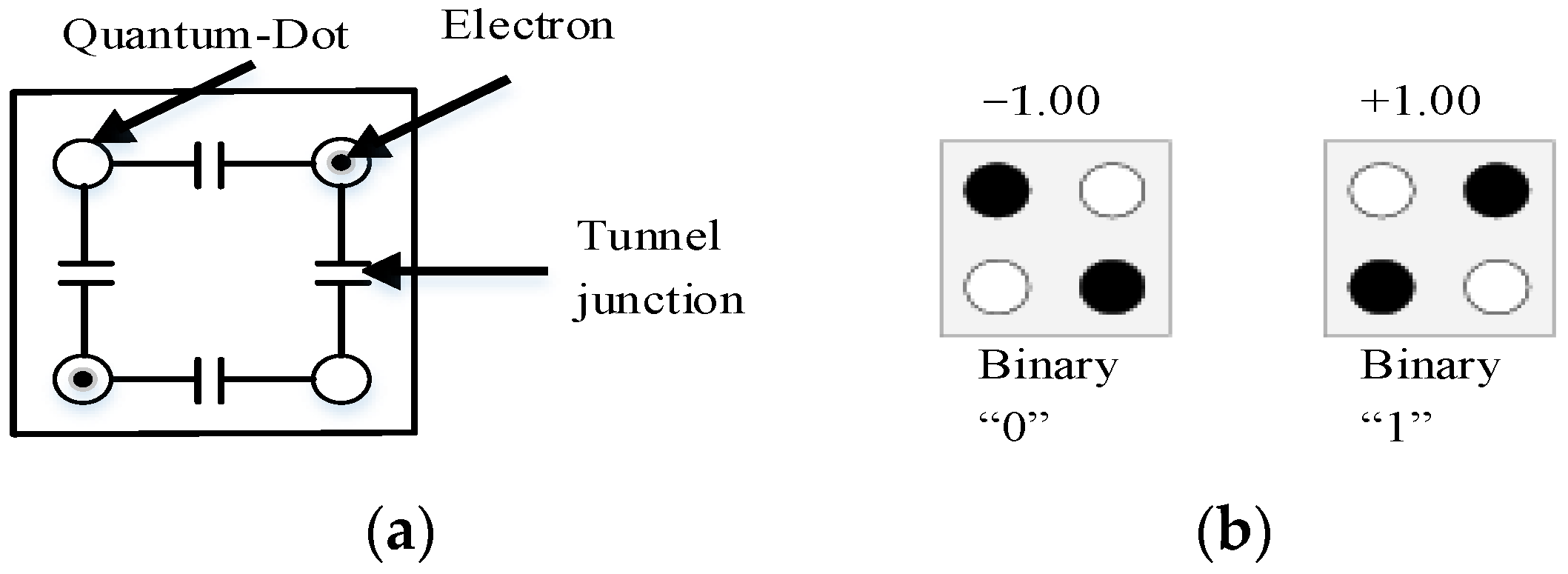
2. QCA Basics
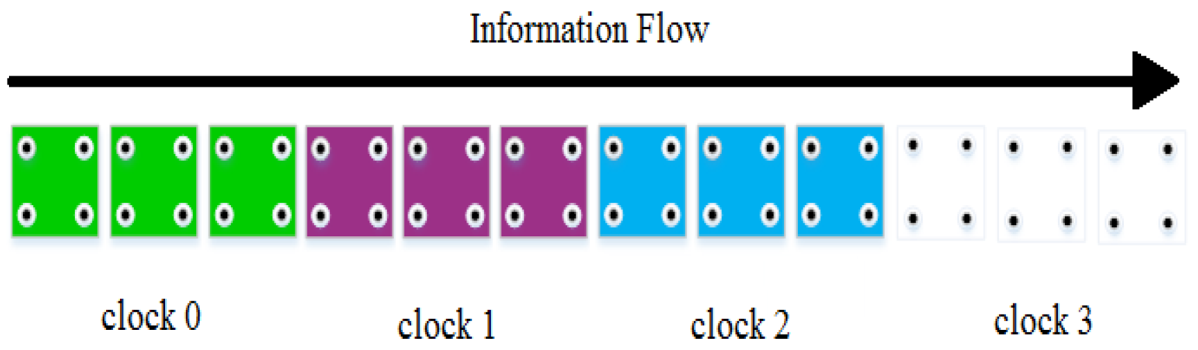
2.1. The QCA Cells Basics
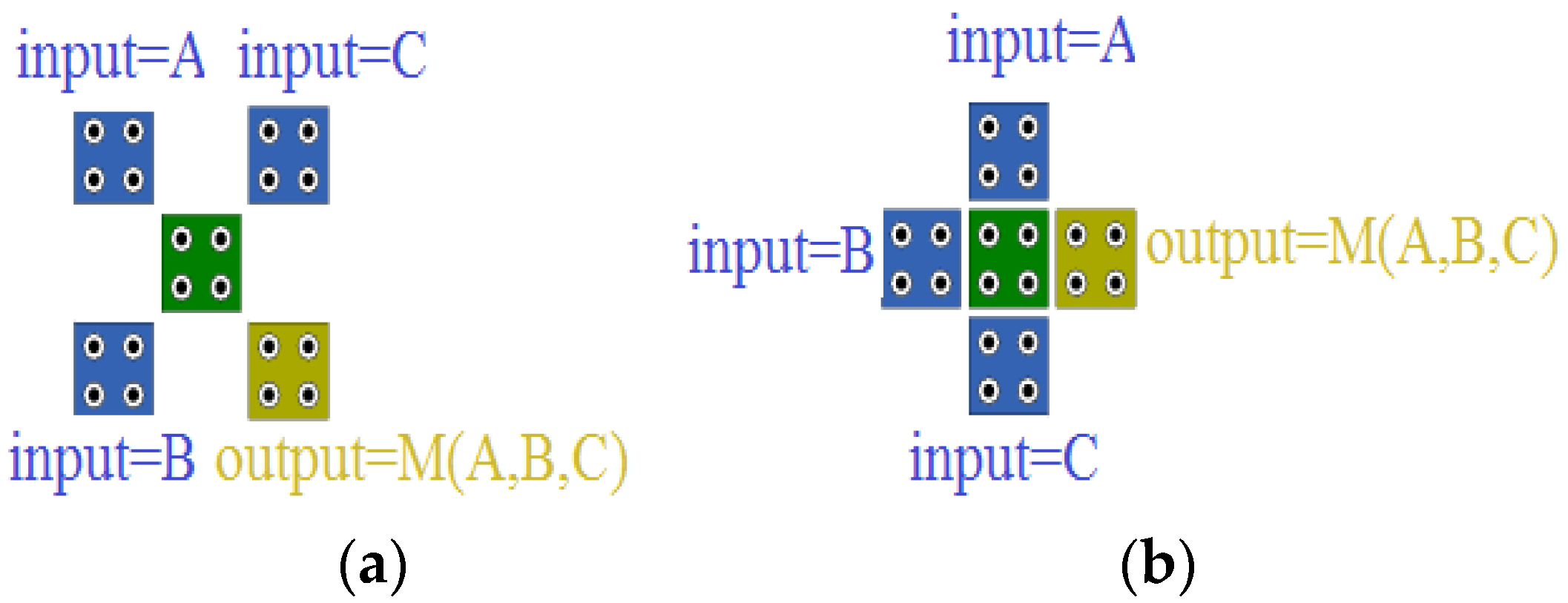
2.2. Overview of FA/RCA Designs
3. The Proposed Circuits
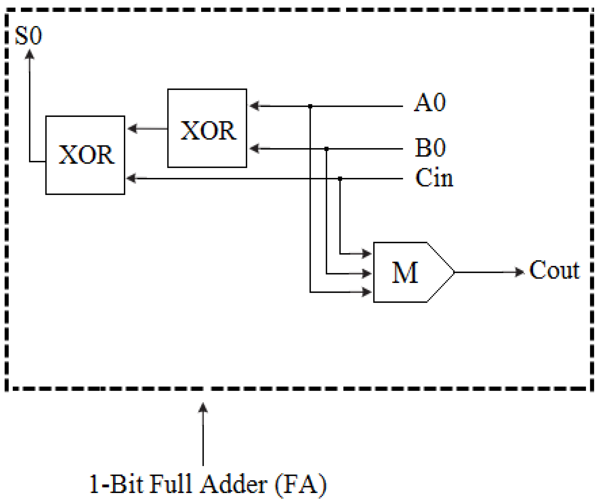
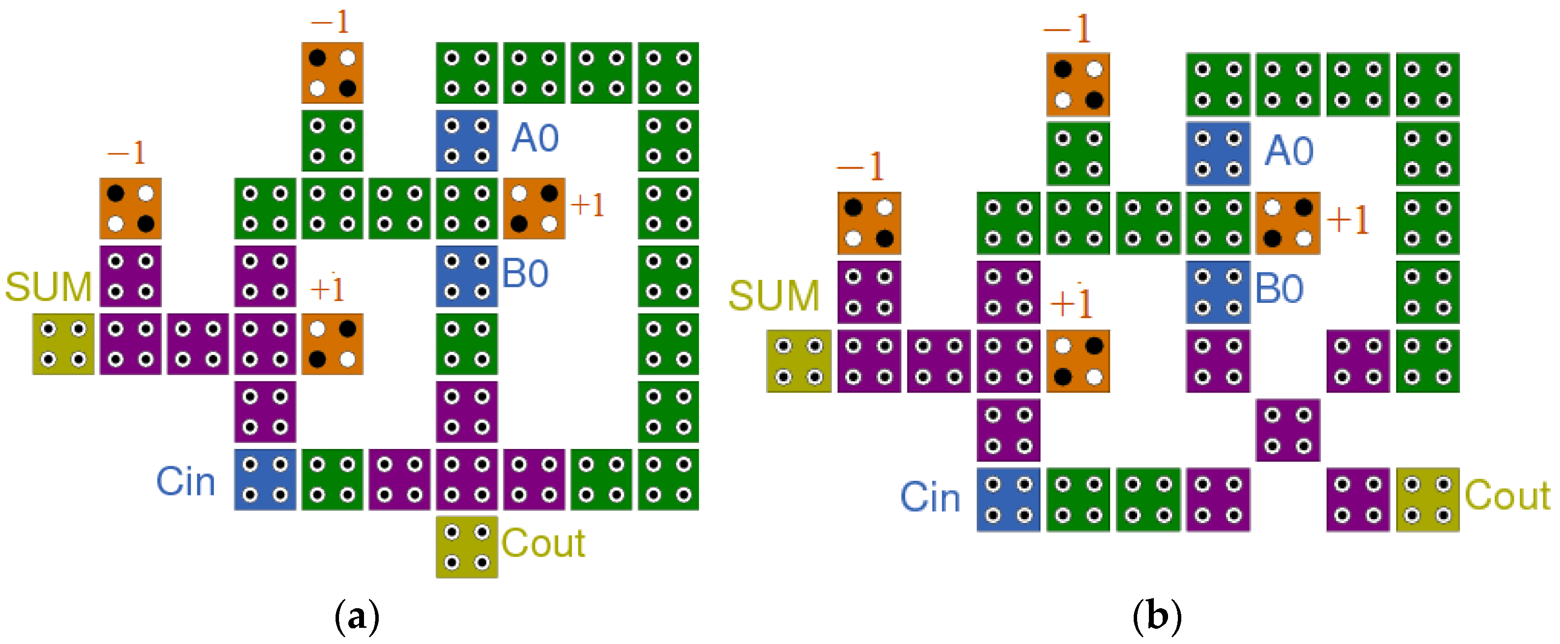
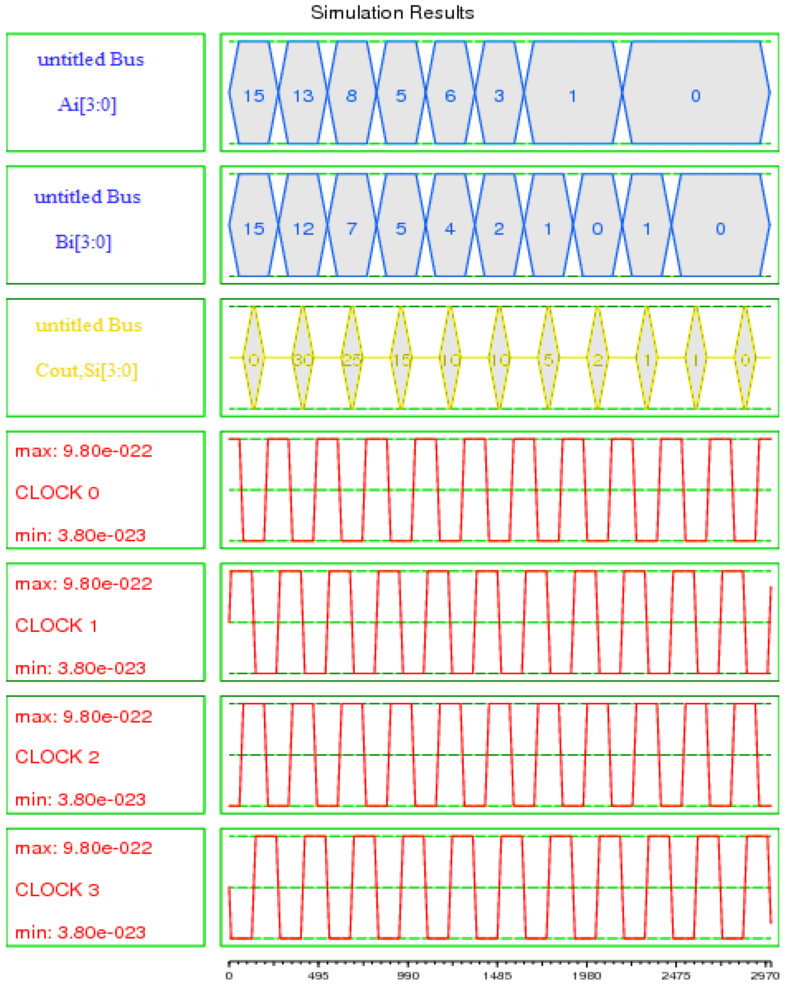
3.1. The FA Circuit Design and Implementation
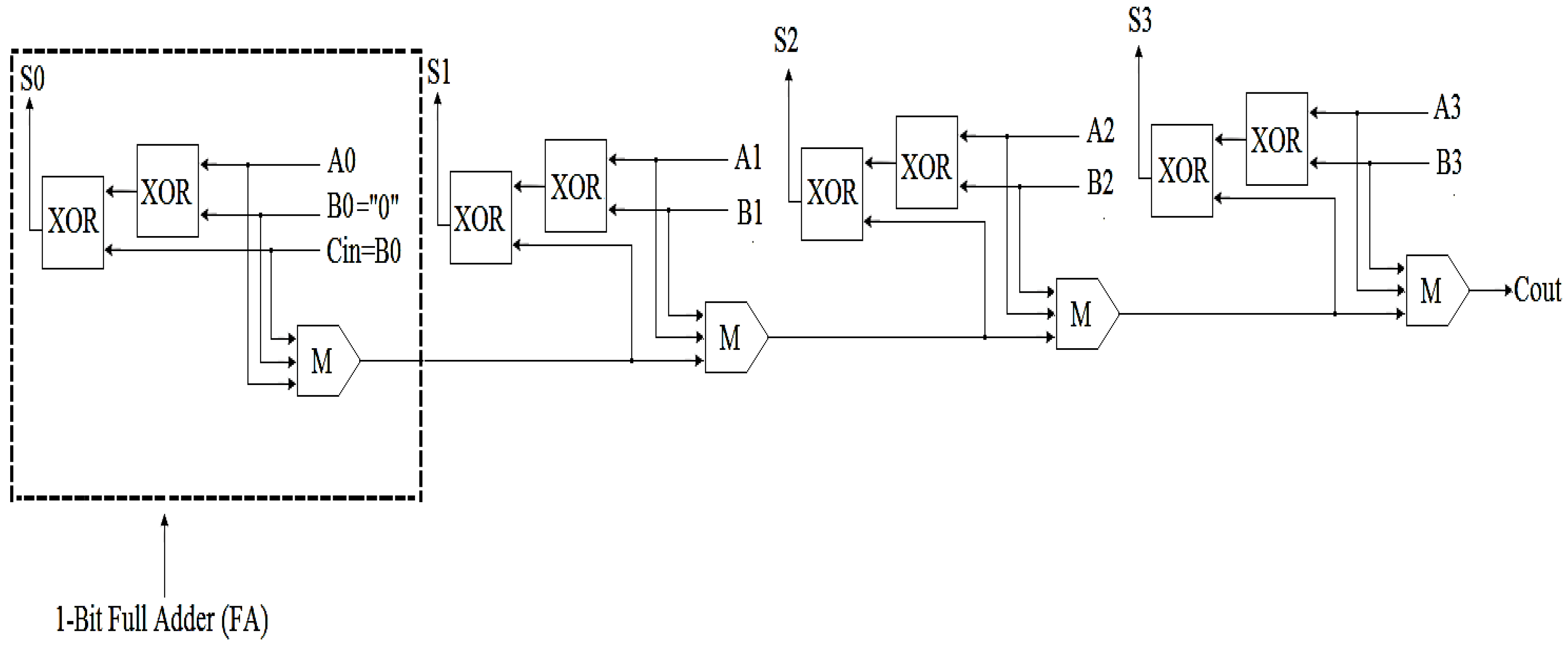
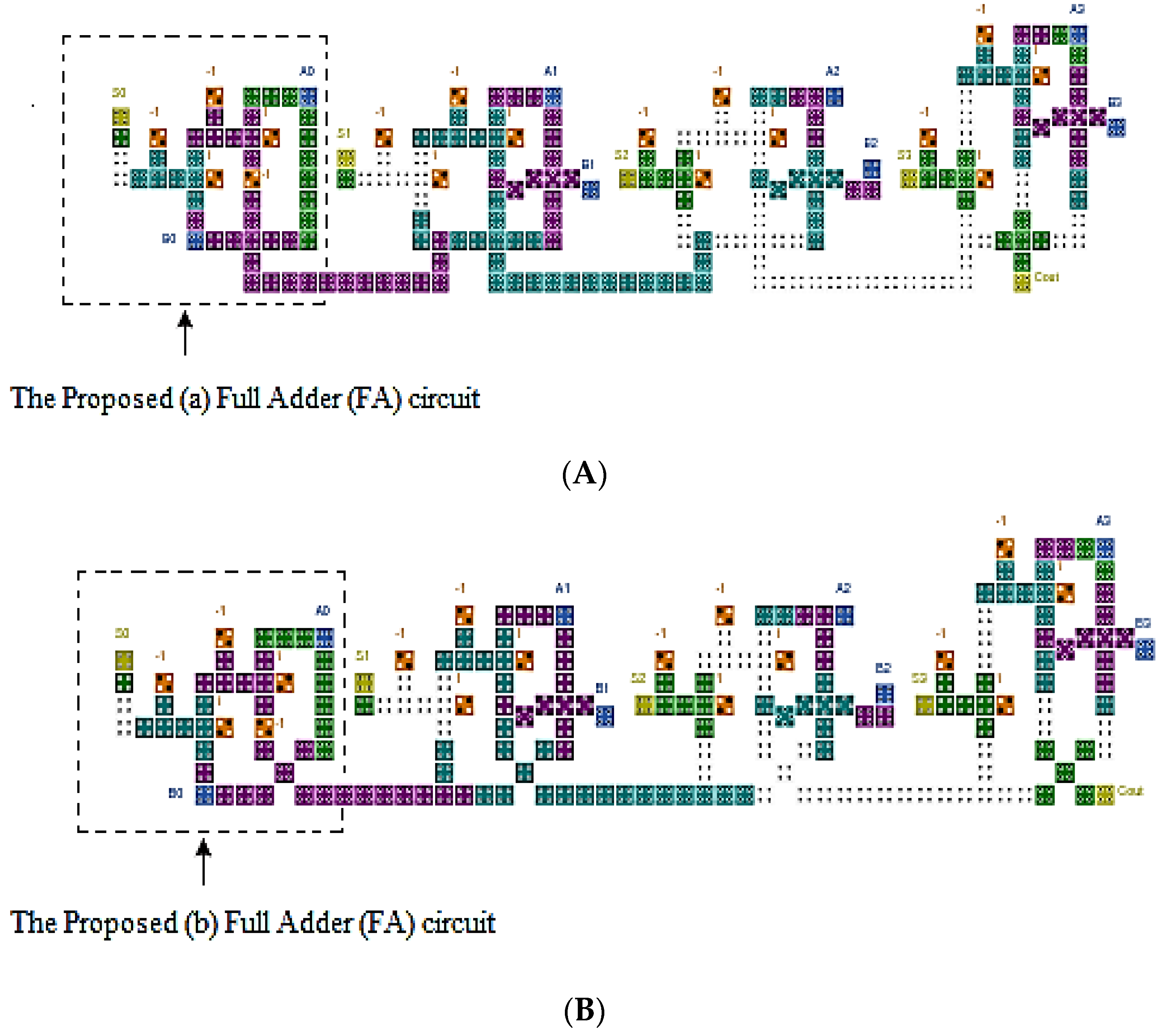
3.2. The RCA Circuit Design and Implementation
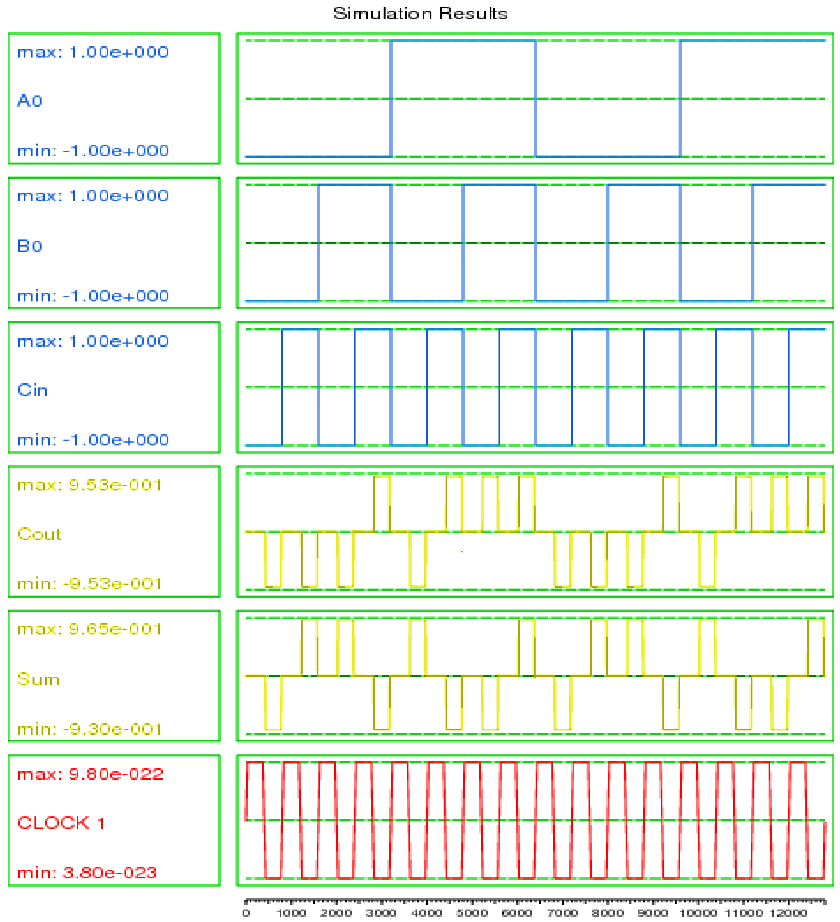
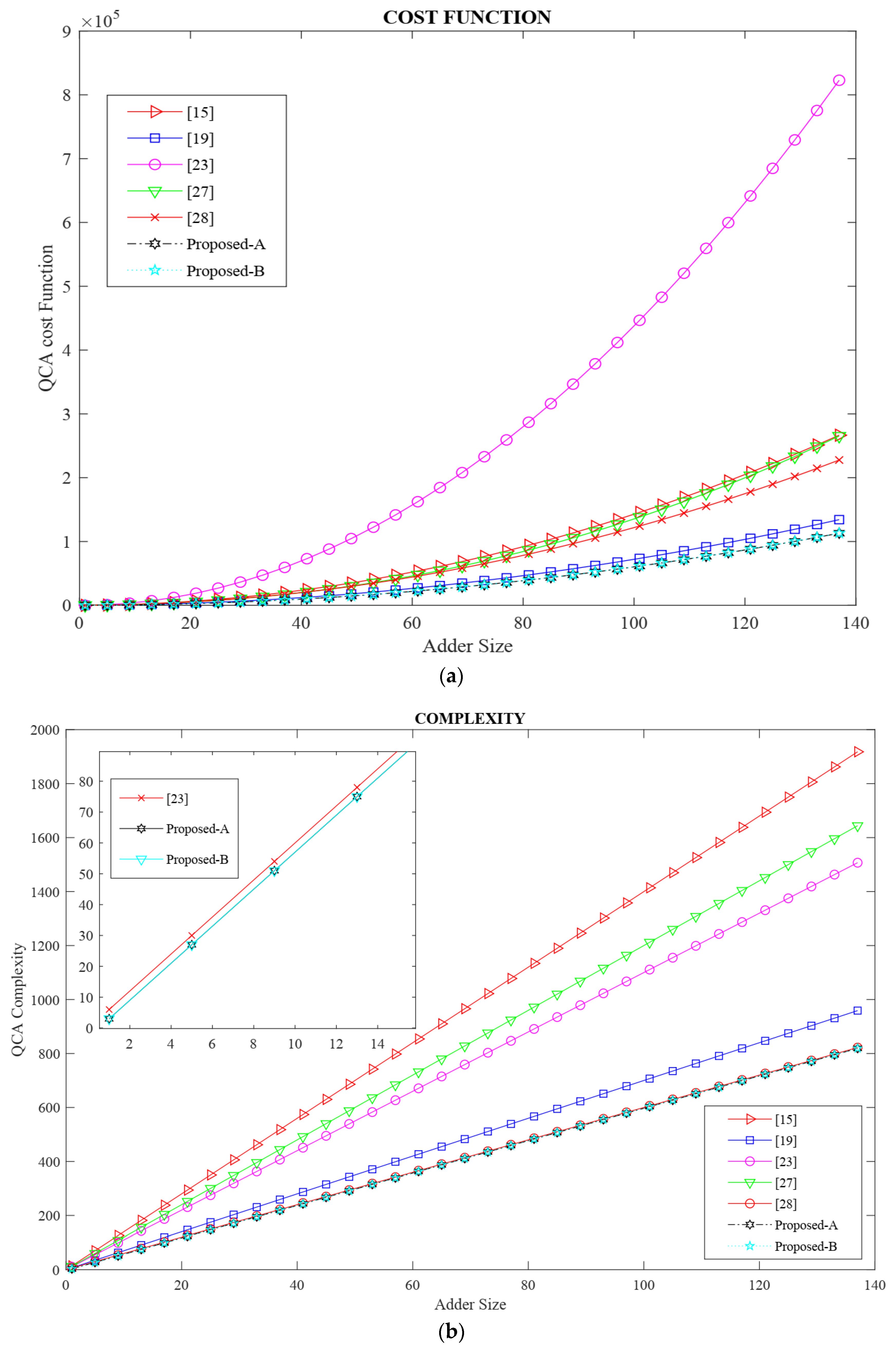
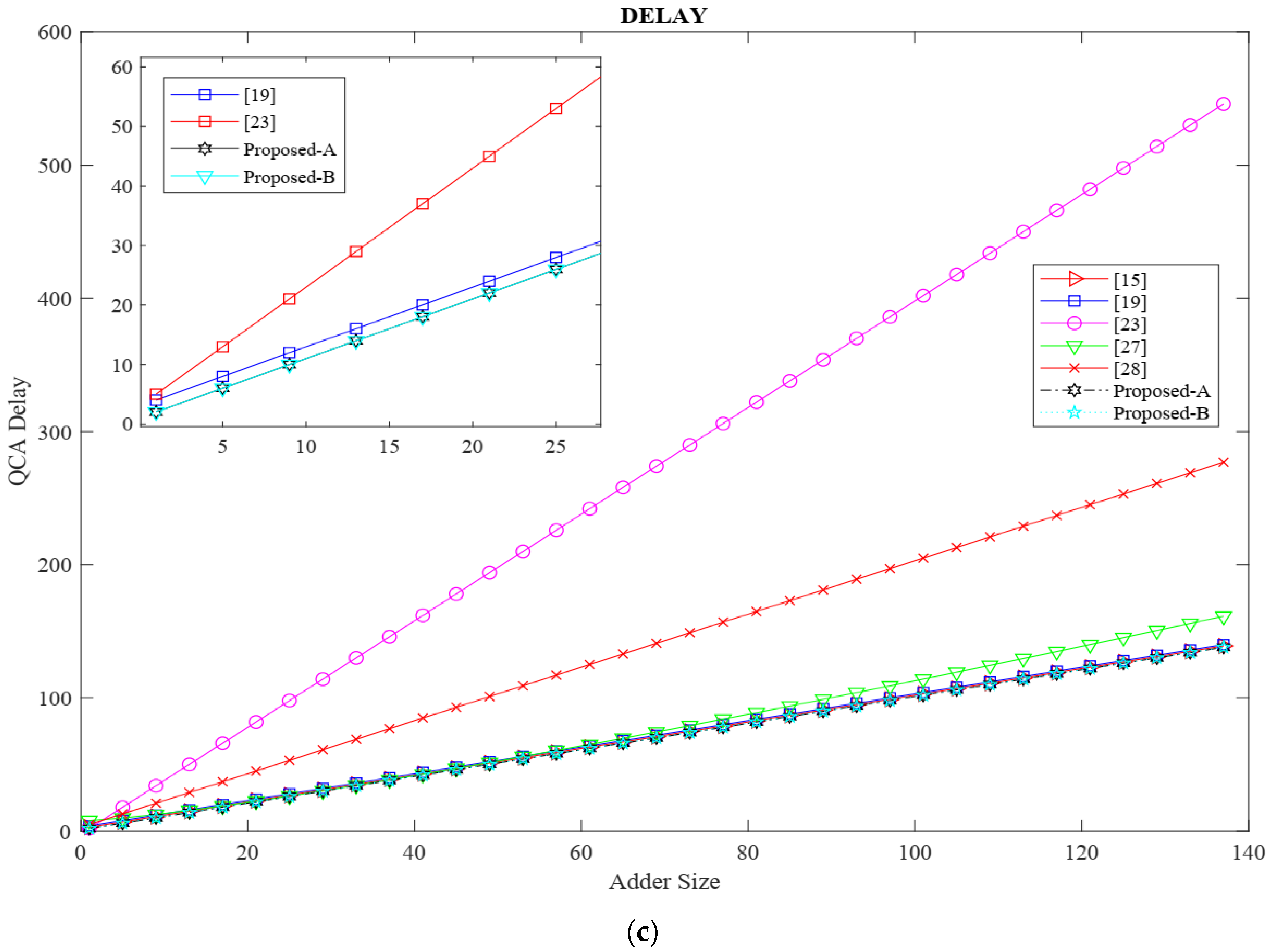
4. Performance Evaluation
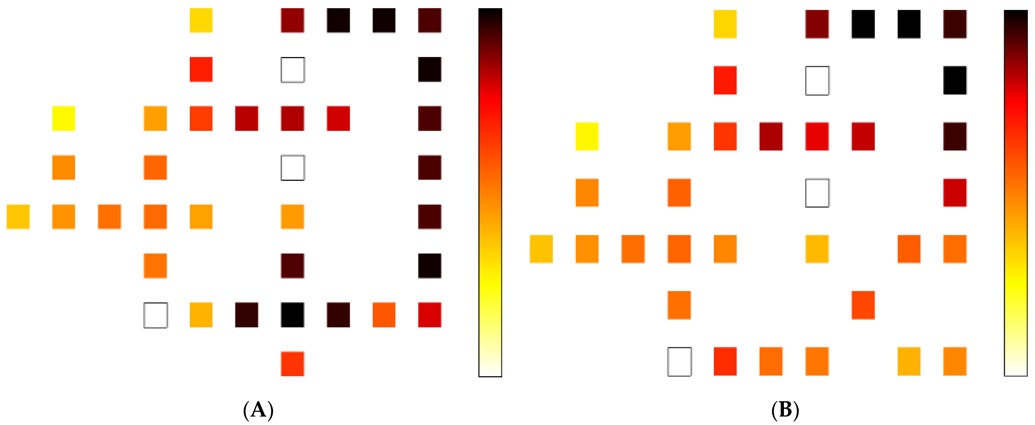
5. Energy Dissipation Analysis
6. Conclusions
Author Contributions
Funding
Institutional Review Board Statement
Informed Consent Statement
Data Availability Statement
Conflicts of Interest
References
- Wang, L.; Xie, G. A Novel XOR/XNOR Structure for Modular Design of QCA Circuits. IEEE Trans. Circuits Syst. II Express Briefs 2020, 67, 3327–3331. [Google Scholar] [CrossRef]
- Snider, E.G.; Orlov, A.O.; Amlani, I.; Zuo, X.; Bernstein, G.H.; Lent, C.S.; Merz, J.L.; Porod, W. Quantum-dot cellular automata: Review and recent experiments (invited). J. Appl. Phys. 1999, 85, 4283–4285. [Google Scholar] [CrossRef]
- Macucci, M.; Gattobigio, M.; Bonci, L.; Iannaccone, G.; Prins, F.; Single, C.; Wetekam, G.; Kern, D. A QCA cell in silicon-on-insulator technology: Theory and experiment. Superlattices Microstruct. 2003, 34, 205–211. [Google Scholar] [CrossRef]
- Edrisi Arani, I.; Rezai, A. Novel circuit design of serial–parallel multiplier in quantum-dot cellular automata technology. J. Comput. Electron. 2018, 17, 1771–1779. [Google Scholar] [CrossRef]
- Vankamamidi, V.; Ottavi, M.; Lombardi, F. Two-dimensional schemes for clocking/timing of QCA circuits. IEEE Trans. Comput.-Aided Des. Integr. Circuits Syst. 2007, 27, 34–44. [Google Scholar] [CrossRef]
- Vahabi, M.; Lyakhov, P.; Bahar, A.N. Design and Implementation of Novel Efficient Full Adder/Subtractor Circuits Based on Quantum-Dot Cellular Automata Technology. Appl. Sci. 2021, 11, 8717. [Google Scholar] [CrossRef]
- Bhargav, A.; Huynh, P. Design and Analysis of Low-Power and High Speed Approximate Adders Using CNFETs. Sensors 2021, 21, 8203. [Google Scholar] [CrossRef]
- Vahabi, M.; Lyakhov, P.; Bahar, A.N.; Wahid, K.A. Design and Implementation of New Coplanar FA Circuits without NOT Gate and Based on Quantum-Dot Cellular Automata Technology. Appl. Sci. 2021, 11, 12157. [Google Scholar] [CrossRef]
- Tougaw, P.D.; Lent, C.S. Logical devices implemented using quantum cellular automata. J. Appl. Phys. 1994, 75, 1818–1825. [Google Scholar] [CrossRef]
- Kim, H.-I.; Jeon, J.-C. Quantum LFSR Structure for Random Number Generation Using QCA Multilayered Shift Register for Cryptographic Purposes. Sensors 2022, 22, 3541. [Google Scholar] [CrossRef]
- Lent, C.S.; Tougaw, P.D.; Porod, W. Quantum cellular automata: The physics of computing with arrays of quantum dot molecules. In Proceedings of the PhysComp 94: Workshop on Physics and Computing, Dallas, TX, USA, 17–20 November 1994; pp. 5–13. [Google Scholar]
- Cho, H.; Swartzlander, E.E. Adder and multiplier design in quantum-dot cellular automata. IEEE Trans. Comput. 2009, 58, 721–727. [Google Scholar] [CrossRef]
- Pudi, V.; Sridharan, K. Low Complexity Design of Ripple Carry and Brent–Kung Adders in QCA. IEEE Trans. Nanotechnol. 2011, 11, 105–119. [Google Scholar] [CrossRef]
- Hayati, M.; Rezaei, A. Design of novel efficient adder and subtractor for quantum-dot cellular automata. Int. J. Circuit Theory Appl. 2014, 43, 1446–1454. [Google Scholar] [CrossRef]
- Mohammadi, M.; Mohammadi, M.; Gorgin, S. An efficient design of full adder in quantum-dot cellular automata (QCA) technology. Microelectron. J. 2016, 50, 35–43. [Google Scholar] [CrossRef]
- Hanninen, I.; Takala, J. Robust adders based on quantum-dot cellular automata. In Proceedings of the 2007 IEEE International Conference on Application-Specific Systems, Architectures and Processors (ASAP), Montreal, QU, Canada, 9–11 July 2007. [Google Scholar]
- Ahmad, F.; Bhat, G.M.; Khademolhosseini, H.; Azimi, S.; Angizi, S.; Navi, K. Towards single layer quantum-dot cellular automata adders based on explicit interaction of cells. J. Comput. Sci. 2016, 16, 8–15. [Google Scholar] [CrossRef]
- Erniyazov, S.; Jeon, J.-C. Carry save adder and carry look ahead adder using inverter chain based coplanar QCA full adder for low energy dissipation. Microelectron. Eng. 2019, 211, 37–43. [Google Scholar] [CrossRef]
- Abedi, D.; Jaberipur, G.; Sangsefidi, M. Coplanar Full Adder in Quantum-Dot Cellular Automata via Clock-Zone-Based Crossover. IEEE Trans. Nanotechnol. 2015, 14, 497–504. [Google Scholar] [CrossRef]
- Sandhu, A.; Gupta, S. Performance evaluation of an efficient five input majority gate design in QCA nanotechnology. Iran. J. Sci. Technol. Trans. Electr. Eng. 2019, 8, 194–205. [Google Scholar] [CrossRef]
- Safoev, N.; Jeon, J.-C. Design of high-performance QCA incrementer/decrementer circuit based on adder/subtractor methodology. Microprocess. Microsyst. 2020, 72, 102927. [Google Scholar] [CrossRef]
- Liu, W.; Lu, L.; O’Neill, M.; Swartzlander, E.E. A First Step Toward Cost Functions for Quantum-Dot Cellular Automata Designs. IEEE Trans. Nanotechnol. 2014, 13, 476–487. [Google Scholar] [CrossRef]
- Moosavi, N.; Navi, K.; Aghazarian, V. Ultra-Low Cost Full Adder Cell Using the nonlinear effect in Four-Input Quantum Dot Cellular Automata Majority Gate. Int. J. Nonlinear Anal. Appl. 2020, 11, 1–16. [Google Scholar] [CrossRef]
- Zoka, S.; Gholami, M. A novel efficient full adder–subtractor in QCA nanotechnology. Int. Nano Lett. 2018, 9, 51–54. [Google Scholar] [CrossRef] [Green Version]
- Majeed, A.H.; Bin Zainal, M.S.B.; Alkaldy, E.; Nor, D.M. Full Adder Circuit Design with Novel Lower Complexity XOR Gate in QCA Technology. Trans. Electr. Electron. Mater. 2020, 21, 198–207. [Google Scholar] [CrossRef]
- Sasamal, T.N.; Mohan, A.; Singh, A.K. Optimal realization of full adder in QCA using 5-input majority gate. In Proceedings of the 2020 International Conference on Industry 4.0 Technology (I4Tech), Pune, India, 13–15 February 2020. [Google Scholar]
- Hashemi, S.; Tehrani, M.; Navi, K. An efficient quantum-dot cellular automata full-adder. Sci. Res. Essays 2012, 7, 177–189. [Google Scholar]
- Balali, M.; Rezai, A.; Balali, H.; Rabiei, F.; Emadi, S. Towards coplanar quantum-dot cellular automata adders based on efficient three-input XOR gate. Results Phys. 2017, 7, 1389–1395. [Google Scholar] [CrossRef]
- Srivastava, S.; Sarkar, S.; Bhanja, S. Estimation of Upper Bound of Power Dissipation in QCA Circuits. IEEE Trans. Nanotechnol. 2008, 8, 116–127. [Google Scholar] [CrossRef]
- Srivastava, S.; Asthana, A.; Bhanja, S.; Sarkar, S. QCAPro-an error-power estimation tool for QCA circuit design. In Proceedings of the 2011 IEEE International Symposium of Circuits and Systems (ISCAS), Rio de Janeiro, Brazil, 15–18 May 2011. [Google Scholar]


| Parameter | Value |
|---|---|
| cell width | 18 nm |
| cell height | 18 nm |
| relative permittivity | 12.9 |
| dot diameter | 5 nm |
| number of samples | 12,800 |
| convergence tolerance | 0.001 |
| clock high | 9.8 × 10⁻²² J |
| clock low | 3.8 × 10⁻²³ J |
| clock amplitude factor | 2 |
| radius of effect | 65 nm |
| layer separation | 11.5 nm |
| maximum iteration per sample | 100 |
| Circuit | Area (µm2) | Cell Count | Latency (clock) | NOT Gate Count | Crossover Type |
|---|---|---|---|---|---|
| FA [1] | 0.057 | 60 | 1 | 1 | not required |
| FA-1 [8] | 0.043 | 45 | 0.75 | 0 | not required |
| FA-2 [8] | 0.037 | 43 | 0.75 | 0 | not required |
| FA [18] | 0.076 | 61 | 0.5 | 4 | coplanar (rotated cells) |
| FA [19] | 0.043 | 59 | 1 | 2 | coplanar (clocking based) |
| FA [20] | 0.047 | 58 | 1 | 4 | coplanar (clocking based) |
| FA [21] | 0.047 | 56 | 1 | 2 | coplanar (clocking based) |
| FA [23] | 0.025 | 37 | 1 | 1 | not required |
| FA [24] | 0.043 | 44 | 1.25 | 6 | not required |
| FA [25] | 0.0.39 | 37 | 0.75 | 2 | not required |
| FA [26] | 0.03 | 37 | 0.75 | 2 | not required |
| Proposed (a) | 0.031 | 37 | 0.5 | 0 | not required |
| Proposed (b) | 0.027 | 35 | 0.5 | 0 | not required |
| Circuit | Area (µm2) | Cell Count | Delay (clock) | Cost | Cost Function P, K, L = 1 |
|---|---|---|---|---|---|
| FA [15] | 0.24 | 237 | 1.5 | 0.36 | 84 |
| FA [19] | 0.29 | 262 | 1.75 | 0.51 | 49 |
| FA [23] | 0.36 | 250 | 2.75 | 0.99 | 66 |
| FA [27] | 0.29 | 308 | 2 | 0.58 | 96 |
| FA [28] | 0.37 | 269 | 3.5 | 1.29 | 154 |
| Proposed (A) | 0.28 | 233 | 1.25 | 0.35 | 26.25 |
| Proposed (B) | 0.25 | 209 | 1.25 | 0.31 | 26.25 |
| FA Circuit | Avg Leakage Energy (meV) | Avg Switching Energy (meV) | Avg Energy Dissipation (meV) | ||||||
|---|---|---|---|---|---|---|---|---|---|
| 0.5 EK | 1 EK | 1.5 EK | 0.5 EK | 1 EK | 1.5 EK | 0.5 EK | 1 EK | 1.5 EK | |
| FA-1 | 11.12 | 32.92 | 58.37 | 49.1 | 42.82 | 36.62 | 60.22 | 75.74 | 94.99 |
| FA-2 | 11.64 | 33.18 | 57.45 | 38.15 | 32.49 | 27.36 | 49.79 | 65.67 | 84.81 |
| FA-[1] | 15.37 | 44.87 | 76.92 | 61.87 | 56.03 | 51.61 | 77.24 | 100.9 | 128.53 |
| FA-[8]-1 | 13.91 | 40.87 | 72.13 | 55.13 | 48.1 | 41.32 | 69.04 | 88.97 | 113.45 |
| FA-[8]-2 | 14.15 | 43.37 | 77.91 | 56.98 | 46.54 | 42.47 | 71.13 | 89.91 | 120.38 |
| FA-[18] | 29.19 | 84.83 | 148.5 | 127.94 | 108.82 | 91.46 | 157.13 | 193.65 | 239.97 |
| FA-[19] | 19.2 | 587.5 | 102.8 | 108.99 | 95.14 | 81.56 | 128.19 | 682.59 | 184.32 |
| FA-[20] | 16.93 | 51.11 | 91.37 | 104.91 | 92.41 | 80.36 | 121.84 | 143.52 | 171.73 |
| FA-[21] | 14.95 | 47.9 | 87.32 | 92.15 | 80.63 | 69.3 | 107.1 | 128.53 | 156.62 |
| FA-[23] | 11.22 | 32.95 | 58.43 | 64.03 | 56.66 | 49.46 | 75.25 | 89.61 | 107.89 |
| FA-[24] | 17.3 | 45.89 | 76.92 | 41.11 | 34.33 | 28.86 | 58.41 | 80.22 | 105.78 |
| FA-[25] | 15.48 | 43.11 | 75.92 | 42.91 | 36.72 | 29.65 | 58.39 | 79.83 | 105.57 |
| FA-[26] | 13.96 | 37.77 | 63.88 | 29.55 | 24.65 | 20.4 | 43.51 | 62.42 | 84.28 |
Publisher’s Note: MDPI stays neutral with regard to jurisdictional claims in published maps and institutional affiliations. |
© 2022 by the authors. Licensee MDPI, Basel, Switzerland. This article is an open access article distributed under the terms and conditions of the Creative Commons Attribution (CC BY) license (https://creativecommons.org/licenses/by/4.0/).
Share and Cite
Vahabi, M.; Bahar, A.N.; Otsuki, A.; Wahid, K.A. Ultra-Low-Cost Design of Ripple Carry Adder to Design Nanoelectronics in QCA Nanotechnology. Electronics 2022, 11, 2320. https://doi.org/10.3390/electronics11152320
Vahabi M, Bahar AN, Otsuki A, Wahid KA. Ultra-Low-Cost Design of Ripple Carry Adder to Design Nanoelectronics in QCA Nanotechnology. Electronics. 2022; 11(15):2320. https://doi.org/10.3390/electronics11152320
Chicago/Turabian StyleVahabi, Mohsen, Ali Newaz Bahar, Akira Otsuki, and Khan A. Wahid. 2022. "Ultra-Low-Cost Design of Ripple Carry Adder to Design Nanoelectronics in QCA Nanotechnology" Electronics 11, no. 15: 2320. https://doi.org/10.3390/electronics11152320