
A Unified and Open LTSPICE Memristor Model Library


Department of Theoretical Electrical Engineering, Technical University of Sofia, blvd. Kl. Ohridski 8, 1000 Sofia, Bulgaria
Electronics 2021, 10(13), 1594; https://doi.org/10.3390/electronics10131594
Submission received: 20 May 2021
/
Revised: 22 June 2021
/
Accepted: 29 June 2021
/
Published: 2 July 2021
(This article belongs to the Section Microelectronics)
Abstract
:In this paper, a unified and open linear technology simulation program with integrated circuit emphasis (LTSPICE) memristor library is proposed. It is suitable for the analysis, design, and comparison of the basic memristors and memristor-based circuits. The library could be freely used and expanded with new LTSPICE memristor models. The main existing standard memristor models and several enhanced and modified models based on transition metal oxides such as titanium dioxide, hafnium dioxide, and tantalum oxide are included in the library. LTSPICE is one of the best software for analysis and design of electronic schemes. It is an easy to use, widespread, and free product with very good convergence. Memristors have been under intensive analysis in recent years due to their nano-dimensions, low power consumption, high switching speed, and good compatibility with traditional complementary metal oxide semiconductor (CMOS) technology. In this work, their behavior and potential applications in artificial neural networks, reconfigurable schemes, and memory crossbars are investigated using the considered memristor models in the proposed LTSPICE library. Furthermore, a detailed comparison of the presented LTSPICE memristor model library is conducted and related to specific criteria, such as switching speed, operating frequencies, nonlinear ionic drift representation, boundary effects, switching modes, and others.
1. Introduction
The resistance switching phenomenon observed in metal oxides such as aluminum oxide, titanium dioxide, tantalum oxide, and others has been analyzed since 1970 [1]. It is related to the process of changing the conductance of the oxide material due to externally applied voltage [1,2]. Such metal oxide materials could retain their conductance and respective state for a long time after turning the electric power source off [2]. These materials can accumulate electric charge proportional to the time integral of the applied voltage and keep the charge if the electric sources are switched off [2]. In this sense, such transition metal oxide materials could be used for creating memory elements [2]. In 1971, Chua predicted the fourth fundamental two-terminal passive electrical element—the memristor [3]. In 2008, the first physical prototype of a memristor was proposed by a Hewlett-Packard research group supervised by Williams [4]. From this moment on, many research groups attempted to produce memristors based on different materials. Some of the successful results are related to polymeric memristors [5], spin memristive systems [6], carbon-based memristors [7], silicon dioxide memristors, and others [8]. Some of the perspective properties of the memristors denoting their potential applications in non-volatile memory crossbars, reconfigurable analog and digital devices, neural networks, and others are their memory effect, high switching speed, low power consumption, nano-scale dimensions, and a sound compatibility to the present CMOS integrated circuit technology [9,10]. In this sense, the memristors based on transition metal oxides are preferred due to their leading properties and indicators [11]. The designing of new and prospective electronic schemes requires preliminary analysis by computer simulations. One preferred software for such analysis is SPICE [12] and its analogues such as LTSPICE, Cadence, and others.
LTSPICE is one of the best products for the analysis, simulation, and design of electronic schemes, circuits, and devices. It is freely available at (https://www.analog.com/en/design-center/design-tools-and-calculators.html#LTspice) (accessed on 16 December 2020). This product is free software with a friendly user interface. It has better convergence than similar products. To the best of the author’s knowledge, there is an absence of complete and suitable SPICE libraries for simulations of different kinds of memristor elements. The main purpose of this paper is to propose to the interested reader a unified and open LTSPICE memristor library containing the main existing and advanced LTSPICE memristor models modified by the author for the analysis of memristor circuits and devices. The proposed library could be expanded by new memristor models, so the readers could enrich the set of suitable models. Another important purpose of this work is to draw comparisons between the considered memristor models and to express their specific advantages, drawbacks, and applications.
The proposed LTSPICE memristor model library with instructions and guidelines for its application are freely available for download and use by readers at: (https://github.com/mladenovvaleri/Advanced-Memristor-Modeling-in-LTSpise) (accessed 16 December 2020).
The rest of the paper is constructed as follows. A brief description of the memristors’ structure and principles of operation is presented in Section 2. The fundamentals of the memristors’ mathematical modeling are presented and discussed in Section 3. The creation of their corresponding LTSPICE models is described in Section 4. Simulation and analysis of several different memristor-based circuits are given in Section 5, where the advantages of the presented models are highlighted. A comparison of the considered memristor models according to several important criteria is presented in Section 6. The discussion and conclusions are given in Section 7.
2. Description of Memristor Structure and Operation in Electronic Schemes
2.1. The Idealized Memristor Element
The ideal memristor element is a passive, two-terminal element. It is a highly nonlinear electric element [13]. It relates the time integrals of the current i flowing through it (the accumulated charge q) and of the voltage v (the so-called flux linkage Ψ). This relation Ψ = Ψ(q) is also called flux-charge relationship [4,11]. It is a nonlinear curve [13]. The amount of electric charges that could be stored into the memristor is limited between its minimal and maximal values qmin and qmax, respectively [11]. The minimal amount of free charges in the memristor is assumed to be zero. The memristor state variable x is proportional to the instantaneous value of the accumulated charge: x = q/qmax. The state variable x is limited in the interval [0, 1]. The system of equations describing the idealized memristor is [3,4,11]:
where k is a constant dependent on the memristor’s physical parameters and properties and M is the instantaneous resistance of the memristor, also called a memristance. The resistance of the memristor could also be expressed as a derivative of the memristor flux linkage Ψ with respect to the accumulated charge q [14]:
The current–voltage characteristic is a pinched hysteresis loop, the area of which decreases when increasing the frequency [14]. The charge–flux relation is an increasing nonlinear curve, which tends to a straight line when increasing the frequency.
2.2. A Description of a Physical Memristor’s Nanostructure
Most memristors considered in recent years are based on transition metal oxides such as titanium dioxide, hafnium dioxide, and tantalum oxide [14]. For this reason, the description of the physical memristor structure in this paragraph is related to memristors based on titanium dioxide and hafnium dioxide [15]. The structure and operation of tantalum oxide memristors is quite different and will be discussed separately [16].
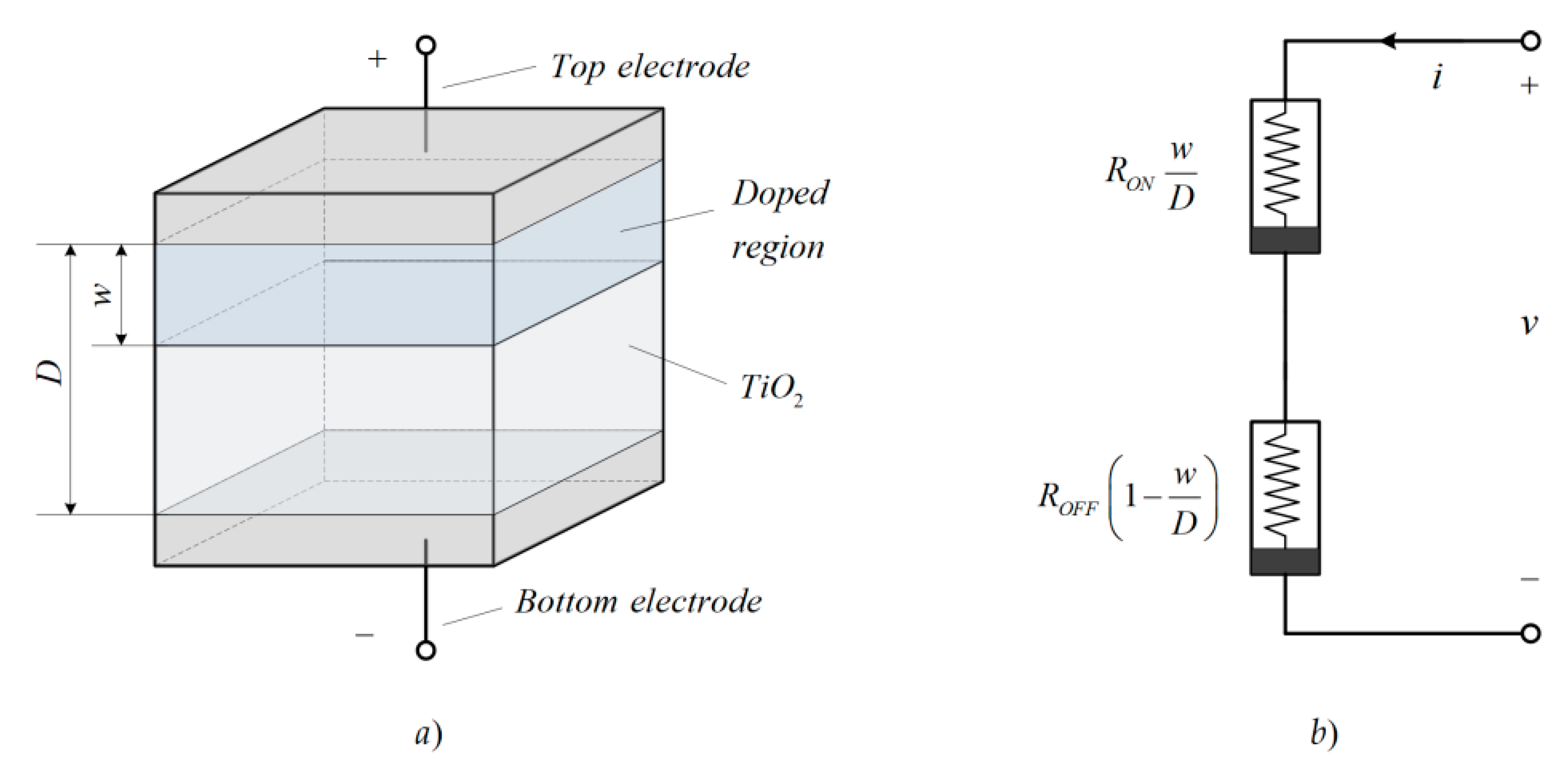
A schematic of the memristor nanostructure is shown in Figure 1a for explaining its operation and properties. This structure is related to memristors based on titanium dioxide and hafnium oxide materials. The electrodes of the element are made of metallic or other material with high conductance [15]. The structure of the memristor is based on a thin layer of amorphous titanium dioxide [4]. The equivalent circuit shown in Figure 1b corresponds to the state-dependent resistances of the doped and un-doped layers of the memristor element.
The top region of the memristor element is created in the titanium dioxide nanostructure by doping it with oxygen vacancies. The bottom layer of the considered element is made of pure titanium dioxide [4]. The oxygen vacancies in the doped layer have a positive electric charge. The doping procedure is known as electroforming, and it is based on applying an external voltage to the memristor nanostructure with a constant value of about 5 V [4]. Owing to the corresponding electric field with a high intensity memristor nanostructure, a partial evaporation of oxygen molecules occurs near the top of the electrode. Then, the oxygen vacancies are generated on the top layer of the memristor [4]. The material of the doped region of the element has a stochiometric chemical formula TiO2−z, where the index z is between 0.02 and 0.05 [4]. The doped layer has low resistance, while the un-doped region has very high resistance [4]. The memristor length denoted by D is between 3 nm and 10 nm. The instantaneous length of the doped layer is denoted by w. It depends on the time integral of the applied memristor voltage [4,11,14].
2.3. Memristor’s Operation in Electric Fields
The doped layer’s length w can be altered by applying external voltage signals [4,11]. If a positive voltage is applied to the memristor, then the anode (top electrode) repels the oxygen vacancies, and they migrate to the bottom electrode (cathode) of the memristor. The doped region’s length increases until the moment when the oxygen vacancies have reached the bottom electrode. If a reverse voltage is applied to the memristor, then the top electrode becomes positively charged with respect to the bottom electrode. The doped layer’s length decreases because the anode attracts the oxygen vacancies [4]. The resistances of the described layers of the memristor depend on their instant lengths w and D-w, respectively, and on their specific conductance [4,11]. If the boundary between the layers reaches the bottom border of the memristor nanostructure, then the length of the doped region has a maximal value. In this state, the memristor has a minimal resistance of 100 Ω [4]. This state of the element is known as a fully closed state. Its respective resistance is known as ON-resistance (RON). If the boundary between the layers of the memristor is on the top border of the memristor nanostructure, then its whole region is based on pure titanium dioxide material and the resistance of the memristor has a maximal value of 16 kΩ [4]. This state of the considered element is known as a fully open state. Its maximal resistance corresponding to this state is known as the OFF resistance (ROFF) [4].
3. Memristor Modeling
Memristor modeling is very important for preliminary analysis and design of memristor-based circuits [16,17]. Each memristor model could be fully described by a system of two equations. The first one is the state differential equation relating the time derivative of the state variable x and the current i (or the voltage v, respectively). The second one is an algebraic equation relating the current i and the memristor voltage v [4,16]. In this section, special attention is paid to the modeling of memristors based on titanium dioxide, hafnium dioxide, and tantalum oxide materials. The main roles of the applied window functions are the limitation of the state variable x in the interval [0, 1], representation the boundary effects, and a partial representation of the dependence between the nonlinear ionic dopant drift and the applied memristor voltage. The models contain several coefficients for adjustment according to experimentally recorded current–voltage characteristics. The procedure for tuning the memristor models is related to a comparison of the simulated and the experimental current–voltage relationships and minimization the root mean square error between them. An example for such a procedure will be presented and discussed in paragraph 3.1.2. The simulations are made on a system with 8 GB RAM and two-core Intel 2.4 GHz processor. A comparison of the considered models according to their operating speed and accuracy will be conducted as well. Follows a brief description of the main existing standard models and the enhanced modified by the author memristor models.
3.1. Titanium Dioxide Memristors’ Modeling
Several standard and modified models for titanium dioxide memristors exist in the scientific literature [4,13,18,19,20,21]. They are abbreviated here as K1–K5 for simplification during the following comparison between them. The modified memristor models discussed here are abbreviated as A1–A5.
3.1.1. Standard Titanium Dioxide Memristor Models
A. Strukov–Williams memristor model (K1) [4]
This memristor model is proposed for analysis of titanium dioxide memristor nanostructures [4]. It uses a simple parabolic window function denoted by fsw(x,i). Due to the fixed ionic dopant mobility µ = 1·10−16 m2/(V·s), it is not able to represent the nonlinear dopant drift according to the applied voltage [4,11,22]. The model is completely described by the next set of Equations (3) and (4). Equation (4) represents the applied window function proposed by Strukov and Williams [4]:
where x is the memristor state variable, k = 1000 is a constant dependent on memristor physical parameters, µ = 1·10−14 m2/(V·s) is the ionic drift mobility, D = 10 nm is the memristor length, Ron = 100 Ω and Roff = 16 kΩ are the ON and OFF resistances of the memristor, v is the applied voltage, i is the memristor current, and f(x) is the window function. In this case, it is presented by Equation (4). The simulation time is about 270 ms and the RMS error is around 6.34 %. The initial value of the state variable x0 needed for solving Equation (3) is in the interval [0, 1] and its usual value is 0.1.
B. Joglekar’s memristor model (K2) [13]
This model is proposed for titanium dioxide memristor nanostructures [13]. It uses a polynomial window function, in which nonlinearity depends on the applied positive integer exponent p. The model is based on a fixed ionic mobility, and it is not able to completely represent the nonlinear ionic dopant drift dependent on the applied memristor voltage. The parameter p is usually between 1 and 100. The model is described by Equations (3) and (5), where the last one represents the Joglekar window [13]:
The nonlinearity of the applied window function and the memristor model increases when decreasing the value of the integer exponent p. The simulation time is 278 ms, and the error is about 5.91%. If p = 1 then the model behaves as the previously discussed Strukov–Williams memristor model [4].
C. Biolek’s memristor model (K3) [18]
This memristor model is based on Equations (3) and (6), where the second one represents a nonlinear and switch-based window function proposed by Biolek [18]:
The integer exponent p is usually between 1 and 100. If the value of p is very high, then the model behaves like the boundary condition memristor model [19] discussed in the next paragraph. The time for simulation is 282 ms and the RMS error is about 5.31%. The original Heaviside step function stp included in (6) is unfortunately a non-continuous and non-differentiable one, and it is replaced by another step-like logistic function for generating the LTSPICE memristor library models for avoiding convergence issues. This model could correctly represent the boundary effects for hard-switching mode.
D. Boundary condition memristor model (Ascoli–Corinto) (K4) [19]
The model [19] described here is based on (3) and (7). The window function represented by (7) is proposed by Corinto and Ascoli [19]:
where vthr = 0.15 V is an activation threshold. This window function ensures a good representation of the boundary effects for hard-switching mode [19,20,23]. The boundary effects occur when the state variable x is zero or unity and they are expressed by (7). In this memristor model, an activation threshold vthr is applied [19,23]. If the applied memristor voltage v is lower than the activation threshold vthr then the state variable x does not change and the memristor behaves as a linear resistor [19,23]. The simulation time is 284 ms and the RMS error is 5.37%.
E. Lehtonen–Laiho model (K5) [21]
This memristor model uses highly nonlinear relationships between the time derivative of the state variable x and between the memristor current i and voltage v, respectively [21]. The model is completely described by the system of Equation (8) [21]:
where β, α, χ, γ, a, m and n are fitting parameters [21,24]. The commonly used values of the integer parameters are m = 5 and n = 5. The other parameters for adjustment are with usual values as follows: β = 150 µA, α = 3.55 V−1, χ = 50 µA, γ = 0.07 V−1, a = 3.34. The standard Biolek window function fB(x,i) is included in the memristor model for representing the boundary effects of hard-switching mode [18]. The simulation time is around 307 ms and the error is approximately 4.24%. The considered memristor model has a good tunability and it is suitable for representation of asymmetric current–voltage characteristics which correspond to a rectifying effect [21].
3.1.2. Modified Titanium Dioxide Memristor Models
The models presented here are based mainly on the previously discussed standard memristor models. The modified models are improved by the author to represent the dependence between the nonlinear ionic dopant drift and the applied memristor voltage [24,25]. Activation thresholds are applied as well. The modified window functions have increased nonlinearity and enhanced ability for tuning the parameters. The optimal values of the tuning parameters are derived using a comparison between experimental current–voltage relationships and the simulated one and varying the models’ parameters till obtaining minimal root mean square error between the i-v characteristics. Another technique applied for confirmation of the results is realizing the memristor models in the MATLAB—Simulink environment [12] and parameters’ estimation using experimental data. An example for the memristor model’s parameters estimation will be discussed in paragraph “E” for the modified model A5. Due to the variation of the memristor physical parameters and chemical structure in the created LTSPICE memristor models, changes of the values of the memristor parameters by the readers are allowed.
A. A modified model with a Joglekar window and a voltage-dependent exponent (A1) [26]
This memristor model uses a modified Joglekar window function. Its positive integer exponent p is a voltage-dependent one [24,26]. This voltage-dependent exponent p(v) is related to the model’s nonlinearity. An activation threshold vthr is also applied to this model [26]. It is fully described by Equation (9):
where b = 10.23 and c = 2.11 are fitting parameters, the function ‘round’ is applied for deriving integer values for the exponent p(v), and vthr = 0.1 V is the activation threshold of the memristor element [24,26]. The simulation time is 283 ms and the error is 4.11%. The main advantages of this memristor model with respect to the original Joglekar model are the use of activation thresholds and the representation of the dependence between the nonlinear ionic dopant drift and the applied voltage by introducing a voltage-dependent integer exponent. A disadvantage of the considered model is its increased complexity according to the standard Joglekar model due to the higher number of mathematical operations in the model [24,26].
B. A modified model with a Biolek window and an additional sinusoidal component (A2) [27]
The modified model presented here is based on the original Biolek model. The applied window function contains an additional sinusoidal component for increasing the nonlinearity of the model [24,27]. Activation threshold vthr = 0.1 V is included in the considered memristor model. It is represented by (10) [25,27]:
where vthr = 0.1 V, p = 5, and m is a fitting parameter. In this model, the positive integer exponent has a fixed value [24]. A very frequently used value of this coefficient is m = 2.34. If m = 0 then the model is transformed in the form of the standard Biolek memristor model [18], i.e., in other words, the classic Biolek model [18] is a special case of the considered modified model [27]. The time for simulation is about 287 ms and the error is 4.03%. The main advantages of the enhanced model [27] according to the standard Biolek model are their improved tunability and increased nonlinearity of the representation of the ionic dopant drift as a function of the applied voltage [24,27].
C. A modified model with Biolek window and a voltage-dependent exponent (A3) [28]
The described memristor model is based on the standard Biolek model [18]. The positive integer exponent p(v) in the window function is a voltage-dependent one [24,28]. The model could realistically represent the dependence between the ionic dopant drift nonlinearity and the applied memristor voltage [24]. Equation (11) represents the model [28]:
where b = 9.53 and c = 2.11 are fitting parameters with positive values [24]. The simulation time is 285 ms and the error is around 3.91 %. The main advantage of the model is the representation of the dependence between the nonlinear ionic dopant drift and the voltage. For this representation, the voltage-dependent integer exponent p(v) is applied [24,28].
D. Modified memristor model with a combined Joglekar–Biolek window function and a voltage-dependent exponent (A4) [24]
This memristor model is based on both the Joglekar and Biolek models. The used integer exponent p(v) is a voltage-dependent one [24,25]. The applied window function is a linear combination of the Joglekar and Biolek window functions. An activation threshold vthr = 0.1 V is included in the described memristor model. It is expressed by the next equation (12) [24,25]:
where b = 9.35 and c = 2.43 are fitting parameters [25]. This model relates the integer exponent p(v) in the window function and the memristor voltage v by a nonlinear relationship [25]. A drawback of this model is its higher complexity compared to the original Joglekar and Biolek models. The simulation time is 281 ms and the error is approximately 3.94%. The advantages are the use of activation thresholds and the representation of the relationship between the nonlinear ionic dopant drift and the memristor voltage by the application of a voltage-dependent positive integer exponent p(v) [24,25].
E. A modified nonlinear Lehtonen–Laiho model with a voltage-dependent Joglekar–Biolek window function (A5) [29]
The model presented here is based on the original Lehtonen–Laiho model [21]. The applied window is a linear combination of Joglekar and Biolek window functions. An activation threshold vthr = 0.1 V is included as well [24,29].
where β = 147 µA, α = 3.23 V−1, χ = 50.2 µA, γ = 0.068 V−1, a = 10.03, and b = 3.05 are fitting parameters.
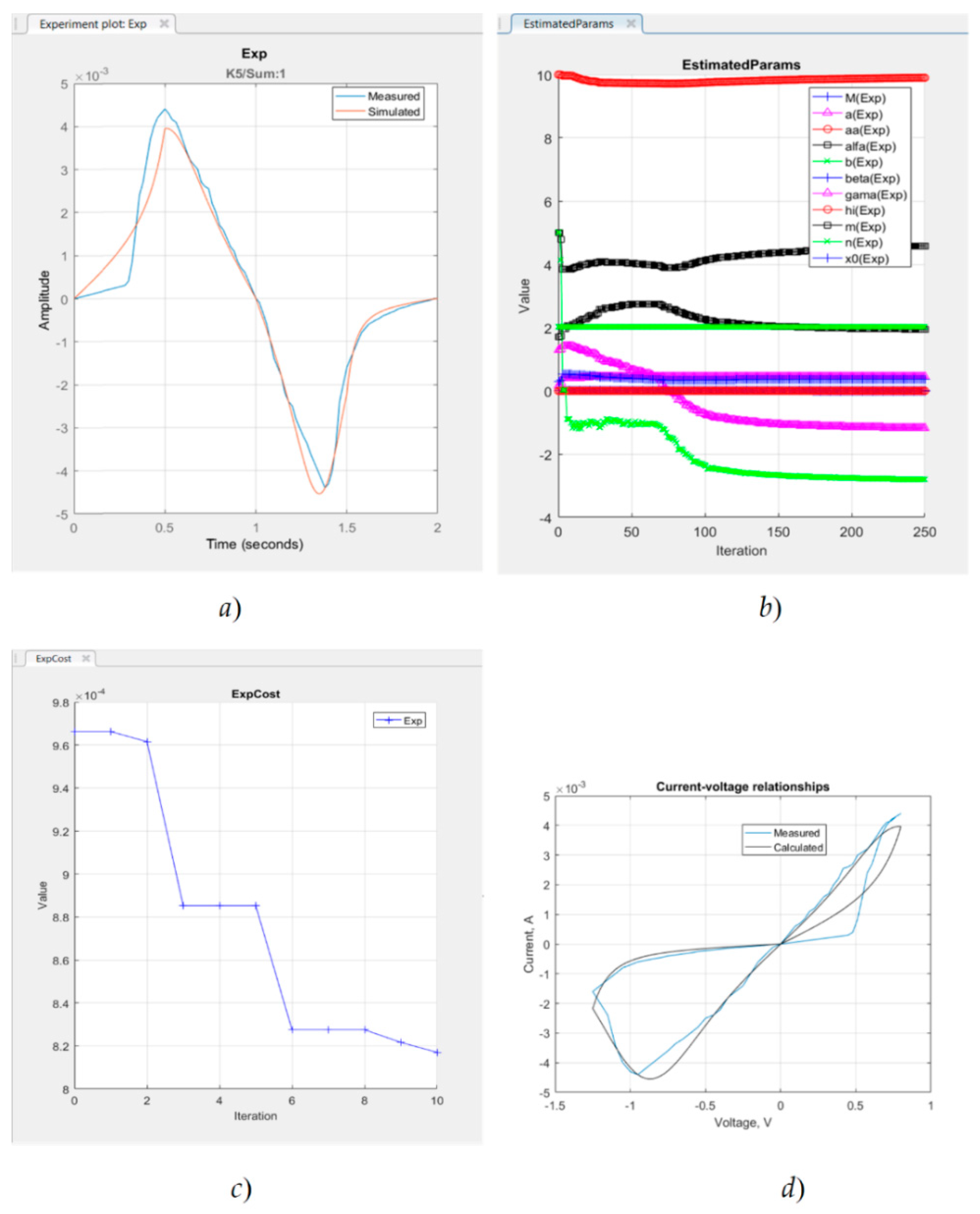
An example for the results obtained by the estimation of memristor model’s parameters using experimental current-voltage relationship is presented in Figure 2. This experiment is conducted in MATLAB and is based on altering the model’s parameters till obtaining a minimal error between the simulated and the experimental i-v relationships. The simulated and the experimental current–voltage relationships of a titanium-dioxide memristor after adjustment of the model A5 are shown in Figure 2a. The change of the model’s parameters during the estimation procedure is presented in Figure 2b. A diagram of the decreasing cost function shown in Figure 2c confirms the correct functioning of the estimation procedure. The corresponding experimental and simulated current–voltage relationships of the considered memristor element presented in Figure 2d are given for visual observation and comparison the results.
This model has higher nonlinearity, and it is suitable for the analysis of memristor circuits for a wide range of frequencies and signal levels [24,29]. The simulation time is 297 ms and the error is 3.38%. The main advantages of this model with respect to the standard Lehtonen–Laiho model [21] is the use of an activation threshold and a window function with increased nonlinearity [24,29]. A disadvantage of this modified memristor model according to its classic analogue is its higher complexity. Bearing in mind the computing speed of modern computers, this little drawback is not so important and can safely be ignored.
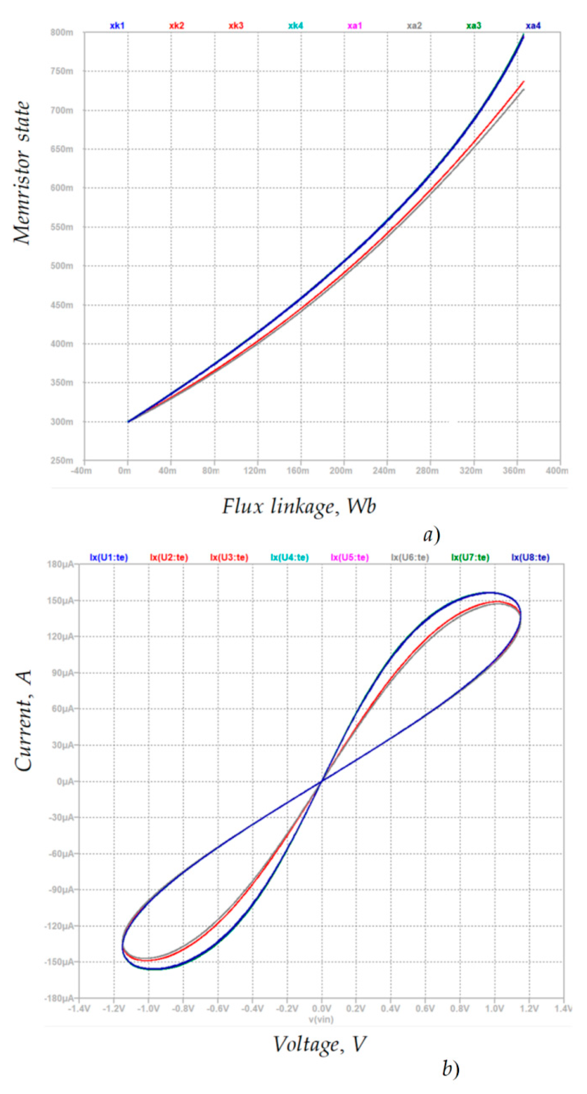
The frequently used standard titanium dioxide memristor models K1, K2, K3, and K4 and the corresponding modified models A1, A2, A3, and A4 are analyzed for sinusoidal voltage signal with an amplitude of 1.15 V and a frequency of 1 Hz. The derived state–flux relationships are presented in Figure 3a for comparison, the considered memristor models and confirmation of their proper behavior. The corresponding current–voltage characteristics derived in the LTSPICE environment are shown in Figure 3b. The respective characteristics have identical behavior. The increased nonlinearity of the dependence between the ionic dopant drift and the applied voltage leads to an increase in the memristor current for models A3 and A4. The behavior of models K5 and A5 is related to the Lehtonen–Laiho model, and it is identical to that of models A6, A7, and A8, which will be discussed in the next paragraph.
3.2. Hafnium Dioxide Memristors’ Modelling
The memristor elements based on hafnium dioxide material are very similar to these made by titanium dioxide owing to the properties of the metals and their oxides. The titanium and hafnium are in the same group in the periodic table, but their properties are not the same due to their different atomic radius and number of electrons. Owing to this, several different and special models for hafnium oxide-based memristors exist in the scientific literature [15].
3.2.1. Standard Hafnium Dioxide Memristor Models
The standard models for hafnium dioxide memristors include activation thresholds. The time derivative of the state variable x is a voltage-dependent quantity [15].
A. Standard hafnium dioxide memristor model with activation thresholds (K6) [15]
This memristor model contains activation thresholds and the ON to OFF and OFF to ON switching times are also included. The time derivative of the state x variable is proportional to the applied memristor voltage v. The model has comparatively low nonlinearity [15].
where vtp = 0.5 V, vtn = −0.5 V are positive and negative activation thresholds, and tswp = 0.11 s, tswn = 0.1 s are ON to OFF switching and OFF to ON switching times, respectively [15]. The ON and OFF resistances are RON = 3 kΩ and ROFF = 45 kΩ. The simulation time is 272 ms, and the error is about 5.14%. A disadvantage of this model is its inability to fully represent the nonlinear dependence between the nonlinear ionic dopant drift and the applied voltage. An advantage of the model is its simplicity for realization [15].
B. Standard hafnium dioxide memristor model with a nonlinear window function and activation thresholds (K7) [15]
The following memristor model used for analysis of hafnium dioxide memristors is more complex than the previous one (K6) due to the use of a highly nonlinear window function [15]. Positive and negative activation thresholds vtp, vtn are applied as well. The simulation time is 291 ms and the error is about 4.14%. A drawback of this model is its higher complexity due to the large number of applied mathematical operations. The model is described by Equation (15):
where CLRS = (ROFF − RON)/tswp, CHRS = (ROFF − RON)/tswn, tswp = 0.1 s, tswn = 0.1 s, PHRS = 1.71, PLRS = 1.73, βHRS = 1.3, βLRS = 1.3, ΘHRS = 1.2, ΘLRS = 1.2, vtp = 0.5 V, and vtn = −0.5 V are fitting parameters [15]. The model has a good tunability. It could partially represent the nonlinear dependence between the dopant drift and the memristor voltage.
3.2.2. Modified Hafnium Dioxide Memristor Models
In this paragraph several hafnium dioxide memristor models improved and modified by the author are presented. The applied modifications are introduced to increase the models’ nonlinearity and representation of the nonlinear ionic drift [30].
A. A modified hafnium dioxide memristor model based on the Lehtonen–Laiho relationship and Biolek window function with additional sinusoidal component (A6) [30]
This memristor model is based on the Lehtonen–Laiho standard model [21] and on the classical Biolek window function [18]. An additional sinusoidal component is included in the modified window function to increase the model’s nonlinearity [30]. An activation threshold vthr is also applied. The positive integer exponent p has a fixed value. The model has high nonlinearity and good tunability. It could be described by the following set of equations:
where β = 60.4 µA, α = 1.38 V−1, χ = 20.2 µA, γ = 1.32 V−1, n = 5, s = 5 and m = 3.2 are tuning parameters [30]. The simulation time is 284 ms and the error is around 3.64%. An advantage of this memristor model is its higher nonlinearity and its ability to correctly represent the ionic dopant drift as a function of the applied voltage [30].
B. A modified hafnium dioxide memristor model based on the Lehtonen–Laiho relationship and Biolek window with a voltage-dependent exponent (A7) [31]
The considered memristor model is based on the standard Lehtonen–Laiho model [21] and on a modified Biolek window function with a voltage-dependent integer exponent [24]. This memristor model could realistically represent the nonlinear ionic dopant drift as a function of the applied voltage [31]. The model is described by (17) [31]:
where β = 61.3 µA, α = 1.35 V−1, χ = 20.7 µA, γ = 1.31 V−1, a = 1.1, b = 10.27, s = 5, n = 5 and c = 3.43 are fitting parameters [31]. The simulation time is 287 ms and the error is about 3.52%. A disadvantage of this model according to the original Lehtonen–Laiho model is its increased complexity. An advantage is its ability to correctly represent the dependence between the ionic dopant drift nonlinearity and the applied memristor voltage [31].
C. A modified model for hafnium dioxide memristors based on Lehtonen–Laiho relationship and Joglekar window with additional sine component (A8) [31]
The memristor model discussed here is based on a linear combination of the standard Joglekar window function [13] and on the classic Lehtonen–Laiho model [21]. An additional sinusoidal component is included in the window function for increasing the model’s nonlinearity [31]. This model is expressed by the next system of Equation (18):
where β = 58.3 µA, α = 1.37 V−1, χ = 21.5 µA, γ = 1.33 V−1 a = 1.12, n = 5, s = 5, d = 1.1 and g = 1.4 are fitting parameters [31].
A drawback of this memristor model is its higher complexity according to the original Lehtonen–Laiho model [21]. The simulation time is about 282 ms and the error is 3.61%. Advantages of the considered model are its increased nonlinearity, better representation of the nonlinear ionic dopant drift as a function of the applied memristor voltage, and good tunability [31].
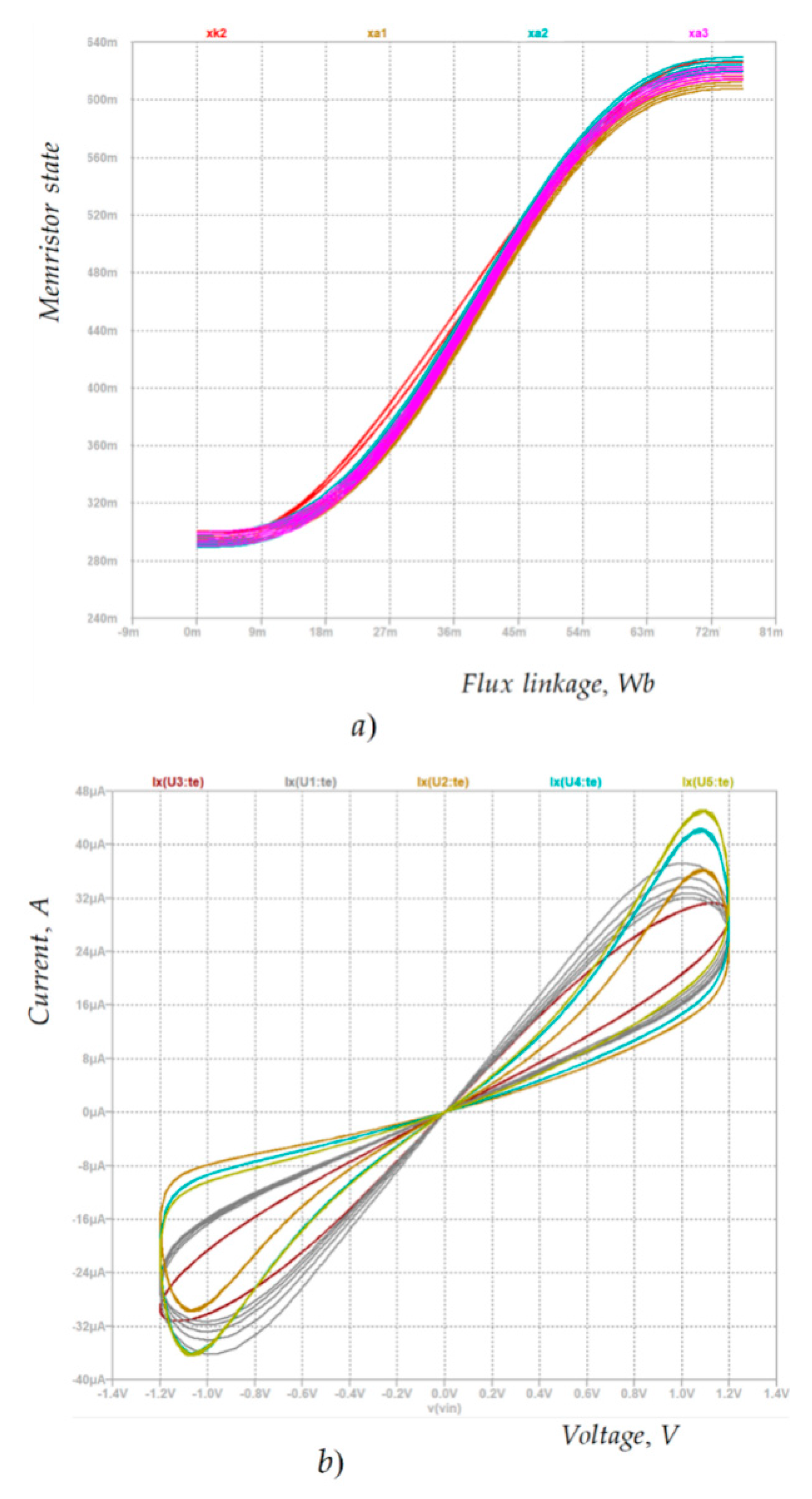
The considered hafnium dioxide memristor models are analyzed for sinusoidal voltage signal in LTSPICE environment for comparison of their basic characteristics and properties. The derived state–flux and current–voltage relationships are presented in Figure 4a,b, respectively. The identical results presented in these figures confirm the tunability of the modified hafnium dioxide memristor models A6, A7, and A8 that are based on the Lehtonen–Laiho model and their suitability for modeling memristors that are based on transition metal oxides. In the considered case, the memristor models are operating in a state near to a hard-switching mode.
3.3. Tantalum Oxide Memristor’s Modelling
According to the description and the corresponding modelling, the memristors based on tantalum oxide are quite different from the considered titanium dioxide and hafnium dioxide memristors [32]. Sometimes several existing models for memristors based on transition metal oxides for the elements of the fourth group of the periodic table are applied for approximated modeling of tantalum oxide memristors [32]. In this paragraph several specialized models for analysis of tantalum oxide memristors are described [32,33,34].
3.3.1. Existing and Standard Tantalum Oxide Memristor Models
These tantalum oxide memristor models are quite complex and are mainly based on the Frenkel-Poole relationship [32].
A. Hewlett-Packard model for a tantalum oxide memristor (K8) [32]
This memristor model was proposed by a Hewlett-Packard research team [32] for the modeling of tantalum oxide-based memristors. It has a high complexity and can be represented by the following system (19) [32]:
where Geq is the equivalent conductance of the memristor, G = 0.025 S is the maximal conductance of the element, xon = 0.06, σp = 4 · 10−5, A = 1 · 10−10 σoff = 0.013 B = 1 · 10−4 xoff = 0.4, β = 500, a = 2.3 · 10−6, and b = 1.6 σon = 0.45 are fitting parameters. The model has high accuracy and correctly represents the nonlinear ionic dopant drift. The simulation time is 343 ms and the error is about 3.24%. A disadvantage of the model is the use of non-differentiable step function and modulus function [32,33]. The application of these functions sometimes is related to convergence problems in the SPICE environment.
B. Standard model of a tantalum oxide memristor with a differentiable modulus-like function and a step-like logistic function (K9) [33]
This tantalum oxide memristor model is based on the previous one [32] but the modulus function and the Heaviside step function are replaced by their continuous and differentiable analogues [33,34] to avoid convergence problems in the SPICE environment. This model is expressed by the next system of Equation (20) [33]:
where k is a fitting parameter. In this case k = 100. The other fitting parameters are the same as in the previous model [32]. This model has a high accuracy [33]. The simulation time is 377 ms and the error is about 3.27%. A disadvantage of this memristor model is its higher complexity with respect to the previous one [32].
3.3.2. Modified tantalum oxide memristor models
The next two enhanced and modified tantalum oxide memristor models have simplified relations between the electrical quantities [35,36].
A. A modified and simplified tantalum oxide memristor model with Biolek window with additional sinusoidal component (A9) [35]
The first modified tantalum oxide memristor model based on [32] and [24] is presented by the following system [35]:
where h and k are fitting parameters [35]. In the present case, h = 0.012 and k = 100. The other fitting parameters in the model are the same as in [32]. The presented memristor model uses a step-like differentiable logistic function instead of the Heaviside step function for avoiding convergence problems in SPICE. The simulation time is 311 ms and the error is about 3.41%. Owing to its simplified expression, the considered model has a higher operating speed compared to the previously discussed tantalum oxide memristor models [35]. The applied window function increases the model’s nonlinearity.
B. A simplified tantalum oxide memristor model with a Biolek window function and a logistic step-like logistic function (A10) [36]
The presented tantalum oxide memristor model [36] is described by system (22).
where the values of the fitting parameters m = 1 · 10−4, k1 = 0.000238, k2 = 0.0002123, h1 = 9.897 · 10−5, h2 = 0.0006531, h3 = 2.88 · 10−5 are found using the curve fitting tool in MATLAB [12]. The other parameters in the model are the same as in [32].
A differentiable step-like logistic function is applied instead of the standard Heaviside step function [32]. Some of the terms in the describing equations are replaced by polynomials for the simplification of the model [36]. Owing to this, the memristor model has a high operating speed. It has good accuracy [36]. The simulation time is 302 ms and the error is about 3.44%. The considered tantalum oxide-based memristor models are tested for sinusoidal voltage signal in LTSPICE to compare their behavior. The derived state–flux and current–voltage relationships are presented in Figure 5a,b for comparison of the models’ properties and characteristics. In the present case the memristors operate in a hard-switching mode. The derived characteristics are identical, and they confirm the correct operation of the tantalum oxide memristor models.
4. LTSPICE Memristor Library Models—Generation and Analysis
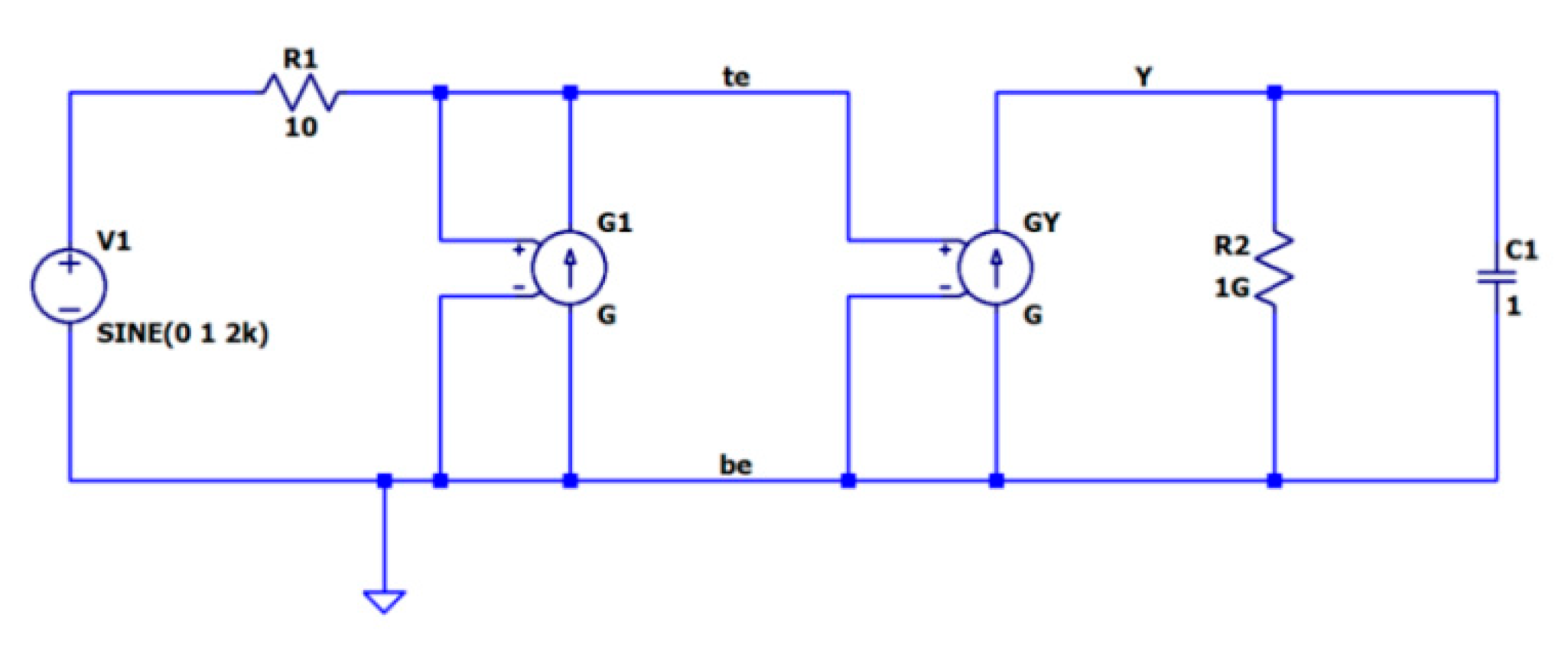
This section presents the LTSPICE realization [12,37] of the considered memristor models. The general LTSPICE equivalent substituting circuit of the memristors is presented in Figure 6 for further description of the considered memristor library models. The schematic presented in Figure 6 is applied for approximate emulation of the behavior of the considered memristors. The top electrode of the memristor is abbreviated by ‘te’ and the bottom electrode—by ‘be’, respectively [36]. In this case, the memristor equivalent schematic is supplied by a sinusoidal voltage source. The memristor current is modeled by the voltage-controlled current source G1, which is taken from the standard LTSPICE library by typing “g”. The current of this dependent source is the memristor current. It is controlled by the memristor voltage, and it flows through the supplying voltage source V1. The internal resistance of the supplying voltage source is expressed by the resistor R1 from the standard LTSPICE library by typing “R”. The additional electrode for measuring the memristor state variable x is denoted by Y. The time derivative of the state variable dx/dt is proportional to the memristor current. It is expressed by the dependent, voltage-controlled current source GY taken from the LTSPICE library by selecting “g”. The capacitor C1 selected from the standard LTSPICE library by typing “C” is connected in parallel to the dependent source GY. This capacitor is used for integrating the current proportional to the time derivative of the memristor state variable dx/dt. The voltage drop across the capacitor C1 is equivalent to the memristor state variable x. The additional resistor R2, selected from the LTSPICE library by typing “R”, has a value of 1 GΩ. It is included in the schematic for avoiding convergence problems during simulations [12,36]. The corresponding LTSPICE netlist code of the memristor model K1 given for further description and example for constructing the library models is presented below.
- 1
- Subckt K1 te be Y
- 2
- Params ron = 100 roff = 16e3 k = 10e3 C1 = 1
- 3
- C1 Y be IC = 0.3
- 4
- R2 Y be 1G
- 5
- Gy 0 Y value = {(k × V(te,be) × (1/(ron×(V(Y)) + roff × (1 − V(Y)))) × (4 × V(Y) × (1 − V(Y))))}
- 6
- G1 te be value = {V(te,be) × ((1/(ron × (V(Y)) + roff × (1 − V(Y)))))}
- 7
- Ends K1
The code presented above is written according to Equation (3) describing the memristor model K1. The first row of the code presented above defines the memristor subcircuit K1, its electrodes “te” and “be”, and the additional electrode Y for measuring the state variable x. The parameters of the memristor model K1 are the ON resistance Ron, the OFF resistance Roff, the constant k, and the capacitance of the integrating capacitor C with their values are presented in the second row. The connections of the elements R2 and C1 between the electrode Y and the bottom electrode “be” and the initial voltage of the capacitor C1 are presented in rows 3 and 4. The fifth row of the code presents the dependent current source Gy, to which controlling voltage is applied between the top electrode “te” and the bottom electrode “be”. The current of the source Gy is proportional to the time derivative of the state variable, and it dominantly flows through the capacitor C1. As the voltage of the capacitor C1 is proportional to the time integral of its current, the potential VY of the electrode Y is proportional to the memristor state variable x. The sixth row of the code corresponds to the state differential equation in (3). The applied state-dependent Strukov–William’s window function fsw(x) = 4x(1 − x) is incorporated in the state differential equation as the fragment “4 × V(Y) × (1 − V(Y))” in the sixth row of the code. It is applied for the limitation of the memristor state variable in the interval (0,1). The dependent current source described in row 6 represents the memristor current dependent on the applied voltage V1 and the memristor state variable x. The final row 7 concludes the LTSPICE code. The code of the memristor library model described above could be converted in a library element in the following way. First, the code must be put in a plain text file and saved as *.txt. Then, this text file must be opened by right mouse button click, selecting “open with” in the context menu and choosing “open with SPICE Simulator w/schematic capture”. Then, the name of the model, in this case K1, must be selected and after a right mouse button click on the selected K1 the option “create symbol” must be chosen. The memristor library element is automatically generated and ready for use in memristor-based circuits. The created memristor library model could be inserted in a new schematic in LTSPICE by the library “AutoGenerated”.
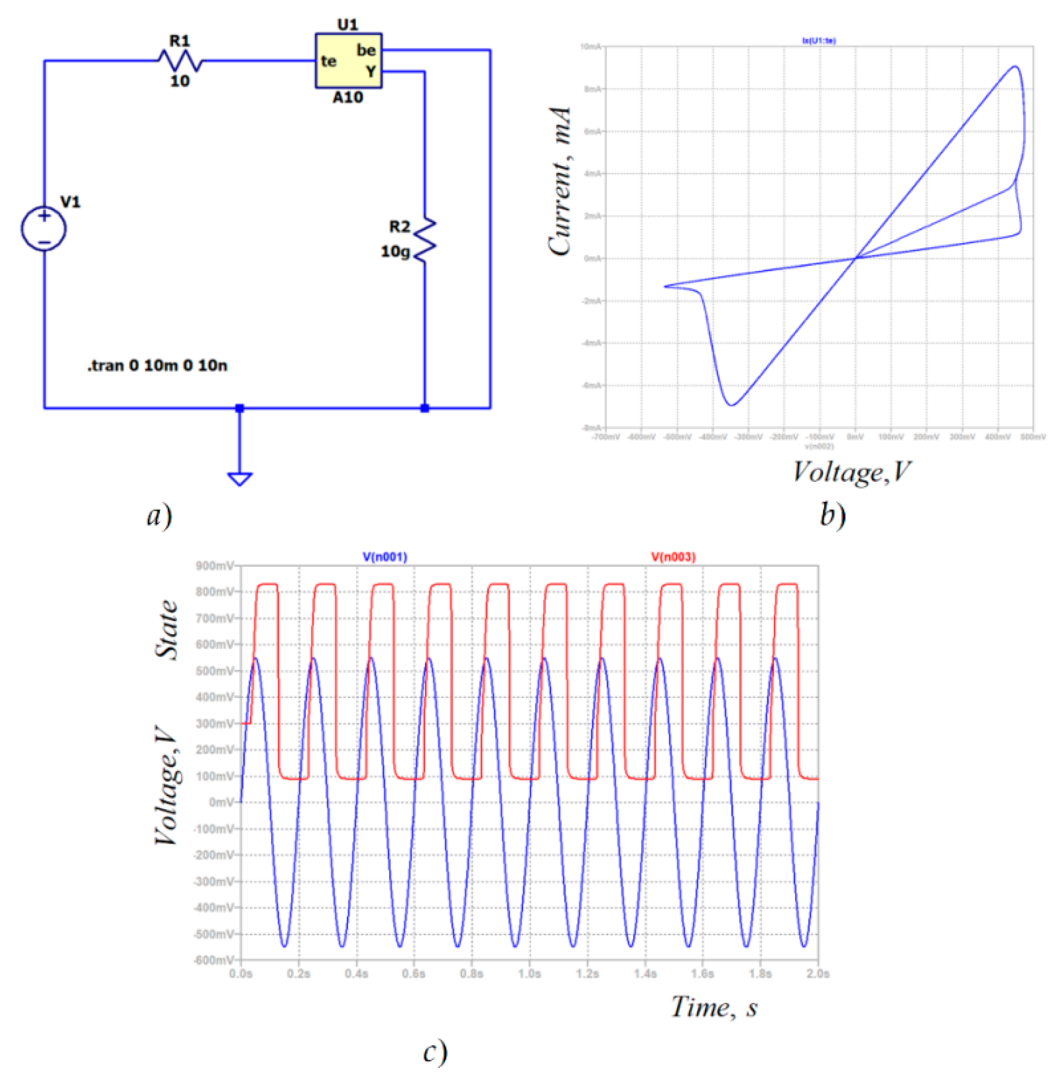
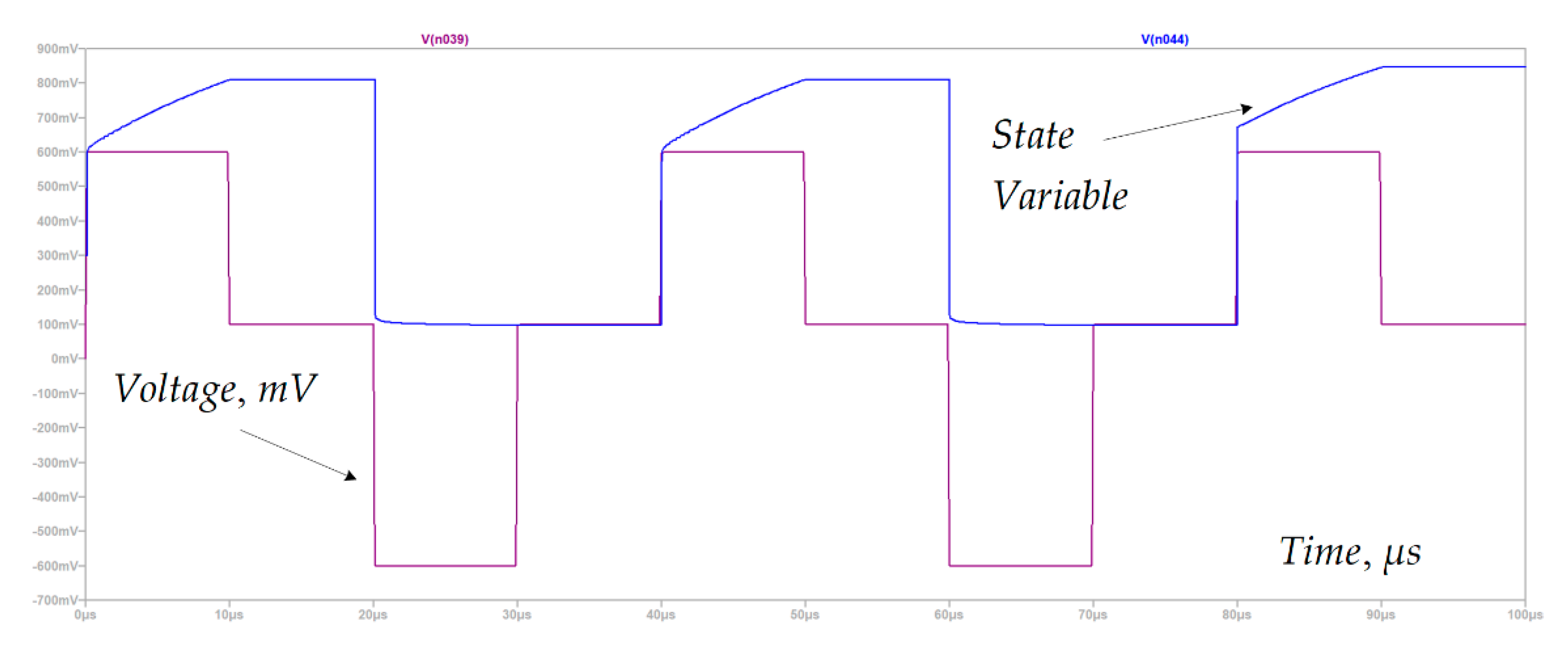
An example of a simple circuit for analysis of memristors is presented in Figure 7a for presenting the applicability and the proper operation of the LTSPICE memristor library models. In this case, the memristor model A10 is applied. The library element contains three terminals–top electrode (te), bottom electrode (be), and an additional electrode Y for measuring the memristor state variable. The current–voltage relationship is shown in Figure 7b. In this case, the memristor operates in a state near to a hard-switching mode. The time diagrams of the applied memristor voltage and the corresponding state variable are presented in Figure 7c for comparison of the change of the state variable and the respective current–voltage relationship for hard-switching mode.
The considered LTSPICE memristor model library is freely available at: https://github.com/mladenovvaleri/Advanced-Memristor-Modeling-in-LTSpise (accessed on 16 December 2020). The interested reader can download it from the link as an archive file, and then the file must be unzipped. The derived folder must be kept on your hard drive disc. After opening the obtained folder, please read the file readme.txt for information. For using the memristor library, previously installed LTSPICE software is needed. It is free software and can be downloaded by the official website of Analog Devices Corporation (https://www.analog.com/en/design-center/design-tools-and-calculators/ltspice-simulator.html#) (accessed on 16 December 2020). The circuit presented in Figure 5 is used for obtaining the netlist of the respective memristor models. The derived netlist is used for the generation of LTSPICE memristor library models.
5. Simulation and Analysis of Memristor-Based Circuits in LTSPICE Environment
In this section an analysis based on simulation of a passive memristor memory crossbar and a simple feed-forward neural network for XOR logical function emulation are conducted. The purpose of this analysis is to confirm the suitability for the considered memristor library models for operation in memristor-based complex electronic schemes in soft-switching and hard-switching mode. For analysis of memristor memory crossbars, the considered tantalum oxide memristor models are applied due to their higher complexity and the operation of the memory cells in a state near to hard-switching mode. The neural network presented in the next paragraph is analyzed using titanium dioxide and hafnium dioxide memristor models owing to their simpler models and the easier analytical expression of the time intervals needed for changing the memristance in a previously determined range.
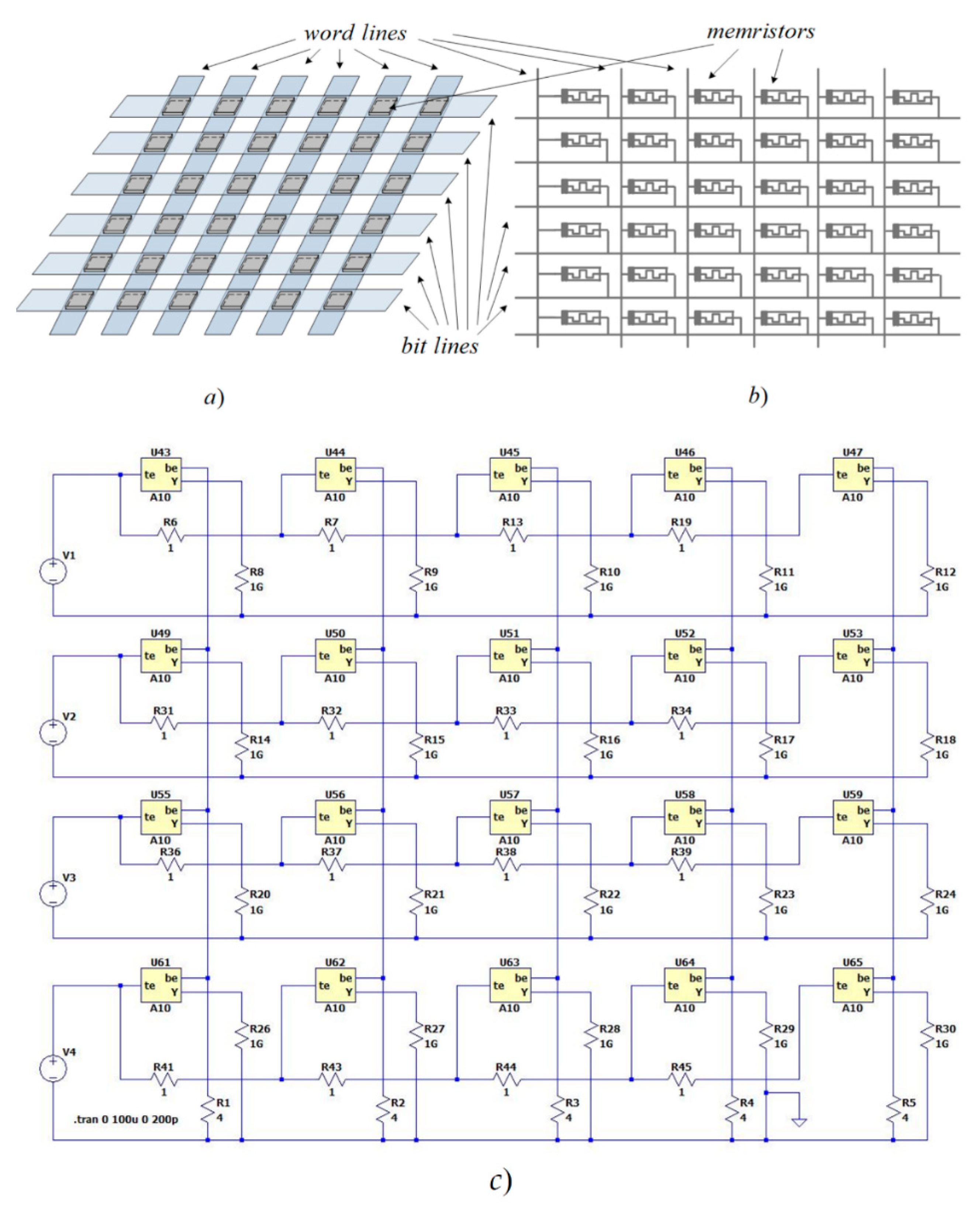
5.1. Analysis of a Passive Memristor Memory Crossbar
A schematic of a passive memristor memory crossbar [38] is presented in Figure 8a. Its electrical equivalent circuit is given in Figure 8b. These circuits are presented for further clarification of the memristor crossbar structure and operation in pulse mode. The memristor memory crossbar under analysis realized in LTSPICE is presented in Figure 8c. The corresponding netlist of the memory crossbar schematic is uploaded in the generated LTSPICE memristor library for additional information at https://github.com/mladenovvaleri/Advanced-Memristor-Modeling-in-LTSpise (accessed on 16 December 2020). The pulse voltage signals for writing, reading, and erasing information in the respective memory cells (the memristors) are applied between the corresponding selected memristor word line and the bit line. Owing to the very high resistance of the memristors in reverse, biasing the sneak path currents does not significantly affect the normal operation of the memory crossbar.
The corresponding time diagrams of the memristor voltage v, the state variable x, and the current–voltage relationship are presented in Figure 9, respectively. These figures are related to model A7, and are shown to illustrate the memristor operation in memory crossbars in a hard-switching mode. The other similar models (K5, A6, A8) have similar behavior. The different levels of the applied voltage are related to the processes for writing, reading, and erasing information in the memristor memory crossbar. The level for writing information is 0.55 V and the duration of the respective voltage pulse is 1 ms. The corresponding change of the memristor state variable is about 0.8 and the change of the resistance of the memristor is about 45 kΩ. For reading the stored information, a positive pulse with the same duration and a level of 0.05 V is applied. During this reading pulse, the state of the memristor and the corresponding resistance does not change so the information is not affected. For erasing the stored information, a negative voltage pulse with a duration of 1 ms and a level of −0.55 V is applied. Owing to the applied negative pulse, the state variable of the memristor returns to its initial value. According to the change of the state variable, the memristor operates in a state near to a hard-switching mode. According to the change of the state variable and the corresponding current–voltage relationships in this analysis, the models K8, K9, A9, and A10 have similar behavior. The memristor model A10 has the highest operating speed with respect to K8, K9, and A9.
5.2. Analysis of a Feed-Forward Memristor-Based Neural Network
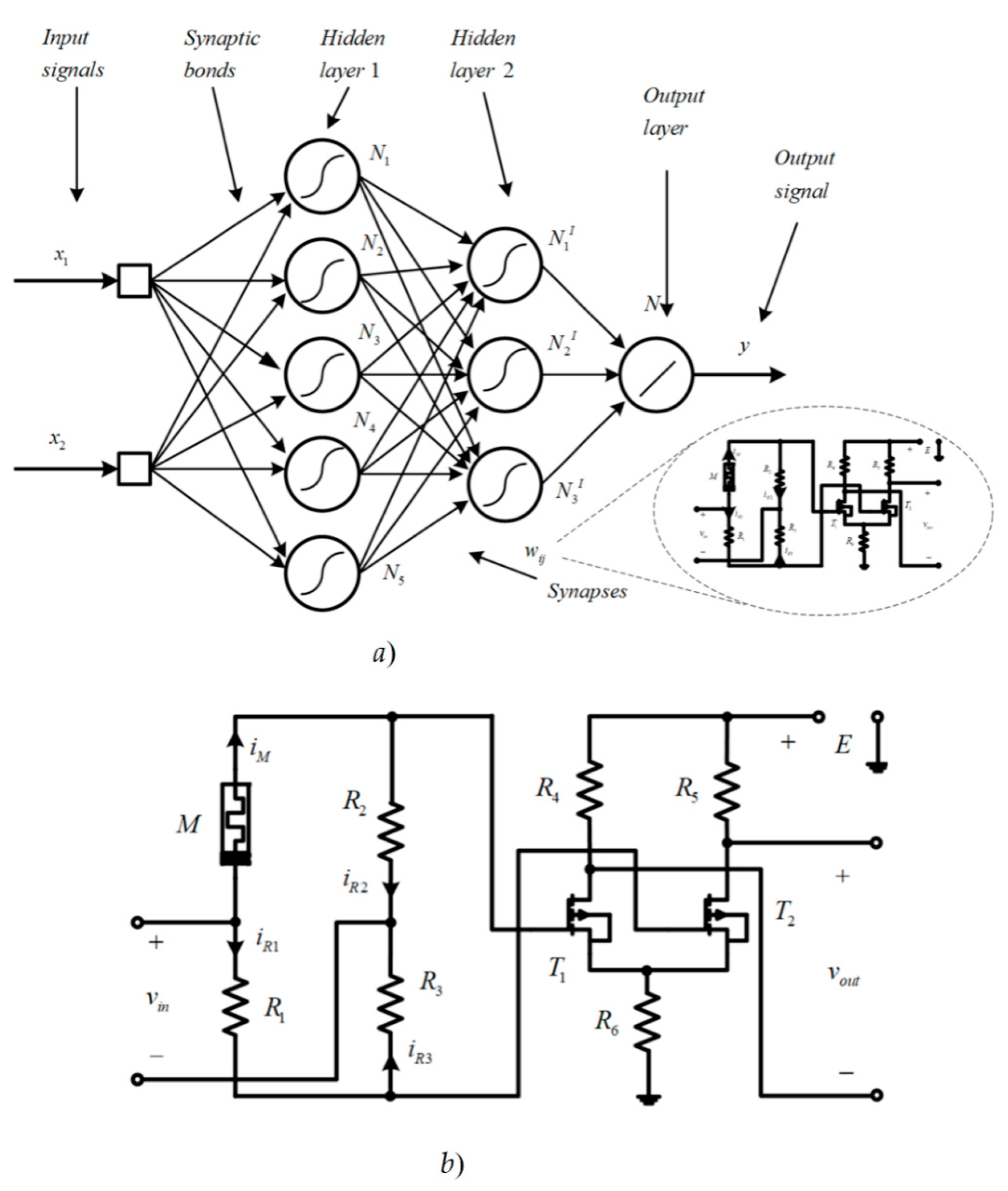
A simple feed-forward neural network for XOR (eXclusive OR) logical function emulation [39,40] is presented in Figure 10a for a description of its structure and operation. Supervised learning is applied for adjusting the synaptic weights. The synaptic bonds are based on memristors. The other elements of the neural network are based on CMOS technology. A detailed diagram of the applied memristor-based synapse is given in Figure 10b for explanation of its schematic and functioning principle. The input pulses are mixed with additive white Gaussian noise signals. The neural network has two inputs corresponding to the signals x1 and x2. It contains two hidden layers and an output layer. The neurons in the hidden layers are with tangent sigmoid activation functions while these in the output layer have linear activation functions. The first hidden layer contains five neurons and the second one has three neurons [35,39,40]. The output layer contains one neuron. The structure of the memristor-based synaptic circuit is presented in Figure 10b [41]. It contains a memristor element M and three resistors connected in a bridge topology and a differential amplifier for scaling the synaptic weights. The differential amplifier is based on two MOS transistors, T1 and T2, and three resistors, R4, R5, and R6. The considered transistors are of type Si4866DY. The transfer coefficient of the differential amplifier is denoted by kv.
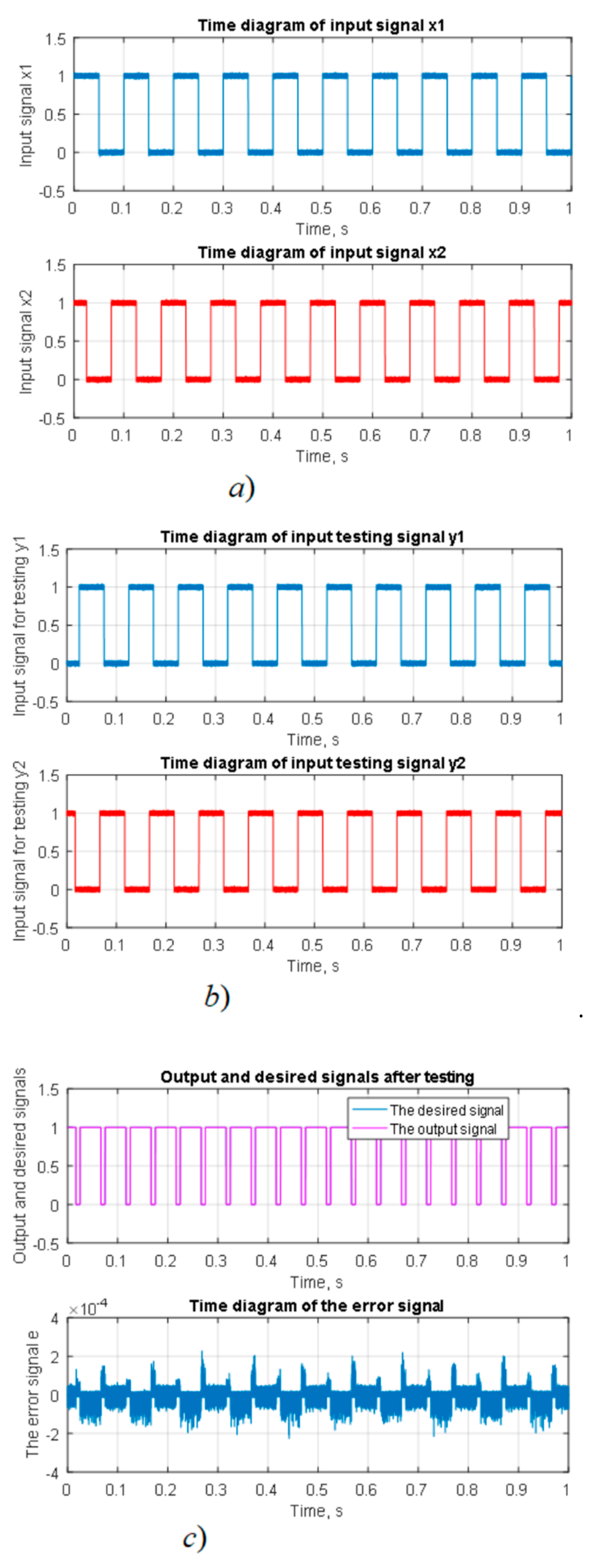
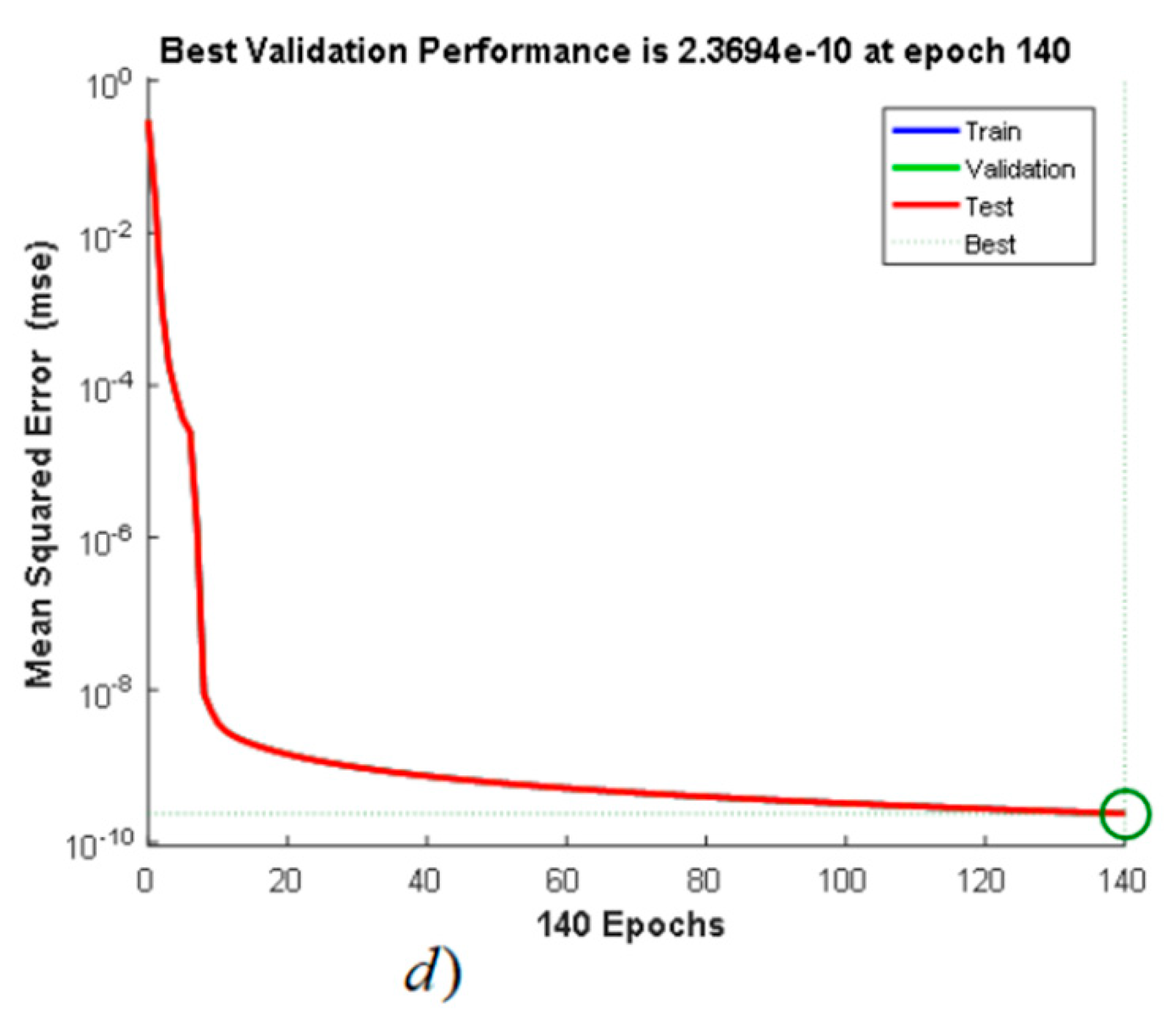
The time diagrams of the input signals x1 and x2 for training the neural network are presented in Figure 11a for visual expression of the logical signals. These signals correspond to logical zeros and ones for the emulation of XOR operation. The signals for testing the neural network are shown in Figure 11b. They are with a different sequence of the pulses according to the training input logical signals. The desired signal and the output signal after testing the neural net are presented in Figure 11c for confirmation of their good coincidence. The error signal is shown in the same figure for visual expression of its very low level. The amplitude of this signal is about one thousand times lower than the input logical signals’ levels. The decreasing of the mean square error during the training process is presented in Figure 11d for confirmation the proper operation of the neural network and the sufficient convergence of the training procedure.
After analysis of the synaptic circuit by the branch current method, the relation between the output voltage vout and the input signal vin is derived:
where kv = 20 is a coefficient presenting the amplification of the differential amplifier. The resistances R1, R2, and R3 are with values of 1 kΩ. Formula (23) shows that the considered memristor-based synapse could ensure positive, zero, and negative synaptic weights [41]. The change of the synaptic weight w is realized by applying external voltage pulses to the synapse and altering the memristance M [41]. The pulses for changing the synaptic weights are applied in the pauses between the samples of the input logical signals x1 and x2. The results presented in Fig. 8 confirm the successful learning and testing of the neural network and its ability to emulate the logical function XOR. The memristor models of titanium dioxide and hafnium dioxide described above are tested in the considered neural network. More appropriate for this analysis are the models K5, A5, K7, A6, A7, and A8 because they are based on the Lehtonen–Laiho memristor model and have a higher operating speed. The other models (K1–K4, K6–K7, and A1–A4) are based on the Strukov–Williams model [4], in which a fixed value of the ionic drift mobility is applied. The exponentially increasing speed of the nonlinear dopant drift as a function of the applied voltage is not expressed in these models, so their operating speed is lower, and they are appropriate for use for low and middle frequency signals.
6. A Comparison of the Considered Memristor Models
Several important criteria related to the comparison of the considered memristor models will be discussed before their comparison [14,23].
The operating frequency is related to the range of the frequency of the memristor voltage where the model operates normally and represents its main memory and switching properties [23]. For the considered memristor models, low frequencies are recognized between 0.5 Hz and 1 kHz, middle frequencies between 1 kHz and 100 kHz, and high frequencies higher than 100 kHz.
The signal levels are related to the values of the memristor voltage ensuring the operation of the element as a switching and memorizing module. Low level voltages are up to 0.9 V, middle level voltages are between 0.9 V and 1.3 V, and high level voltages are greater than 1.3 V.
The nonlinearity of the memristor model is a measure of both the deviation of the current–voltage characteristic and the deviation of the relationship between the ionic dopant drift and the voltage from a straight line.
The accuracy of the memristor model is its ability to precisely represent the current–voltage characteristic with respect to experimental data with minimal deviation and root mean square (RMS) error. If the obtained RMS error is up to 4% the accuracy is recognized as high, if the RMS error is between 4% and 6% the accuracy is satisfactory, and for RMS higher than 6% the accuracy is assumed to be low.
If the memristor voltage is lower than the activation threshold, then the state variable does not change and the memristor behaves as a linear resistor. If the voltage is higher than the activation threshold then the state variable of the memristor changes according to the time integral of the current. The activation threshold depends on the physical properties of the memristors. For the considered memristor models it is between 0.1 V and 0.45 V.
The operating mode is related to the range of altering of the state variable. If the state variable changes in a narrow range and does not reach the boundaries, then the memristor operates in a soft-switching mode. If the state variable changes in a broad range and reaches the boundaries, then the memristor operates in a hard-switching mode.
The boundary effects are related to the memristor operation in a hard-switching mode. If the state variable is zero and the voltage is lower than zero, then the state variable remains zero owing to physical restrictions. If the state variable is zero and the voltage is higher than zero, then the state variable increases. When the state variable is equal to one and the voltage is lower than zero then the state variable decreases. If the state variable is equal to one and the voltage is higher than zero, the state variable remains at a value of one due to the memristor’s physical limitations.
The nonlinear ionic dopant drift, which is dependent on the applied memristor voltage, is a nonlinear and increasing function.
The tunability of the memristor model is its suitability for adjustment according to experimental current–voltage characteristics.
The complexity of the memristor model is a measure of the presence of several elementary mathematical operations and the related computation time for simulating the model with given signals.
The application of the memristor model is related to the areas of the technical fields where the model is applicable—for example, for analysis of memories, neural networks, reconfigurable analog and digital devices, and others.
Table 1 represents a brief comparison between several existing and modified titanium dioxide memristor models according to the criteria presented above. Table 2 is related to the standard existing and modified hafnium dioxide memristor models. Table 3 is related to models of tantalum oxide memristors. The main properties and advantages of the considered models are highlighted.
7. Discussion and Conclusions
The proposed unified and open LTSPICE library models could be useful for the readers who are interested in the analysis and design of memristor-based schemes and devices. The considered models are mainly related to memristors made of transition metal oxides. In the near future, new memristor models for memristors based on perspective materials will be incorporated easily to enrich the library content and comparison of the different types of memristors. The considered models could be applied easily by the readers and tested in different electronic memristor-based circuits and devices. The modified models have better tunability and increased nonlinearity with respect to their standard analogues and could be applied to the design of memristor circuits.
LTSPICE is widely used in the engineering and scientific teams for preliminary analysis and design and simulations of electronic circuits and devices. According to the intensive research on memristors and memristor-based circuits in recent years for application in neural networks, memories, reconfigurable devices, and for in-memory computing, a unified LTSPICE memristor library is described in this paper. The library is freely available for use by the readers, and it could be expanded by new memristor models. The memristor models included in the considered library are related to the main applied materials—titanium dioxide, hafnium dioxide, and tantalum oxide. The proposed LTSPICE library contains the basic and frequently used existing standard and modified memristor models. The main contributions according to the memristor models enhanced by the author are the modification of several window functions by introducing a nonlinear dependence between the positive integer exponent and the memristor voltage, adding a sinusoidal component for increasing the nonlinearity of the window functions, and the simplification of several models for increasing their operating speed. A comparison of the considered standard and modified memristor models is conducted. The main advantages and common potential applications of the models are highlighted. The readers interested in simulation and analysis of electronic circuits and devices based on memristors could download and test the proposed models. Feedback related to the operation of the memristor models and proposals for their improvement or for new memristor models could be useful for enriching the considered LTSPICE library.
Funding
This research received no external funding.
Conflicts of Interest
The author declares no conflict of interest.
References
- Dearnaley, G.; Stoneham, A.M.; Morgan, D.V. Electrical phenomena in amorphous oxide films. Rep. Prog. Phys. 1970, 33, 1129–1191. [Google Scholar] [CrossRef] [Green Version]
- Chiu, F.C. A Review on Conduction Mechanisms in Dielectric Films. In Advanced Materials Science Engineering; Hindawi Publishing Corporation: London, UK, 2014; Volume 2014, pp. 1–18. [Google Scholar] [CrossRef]
- Chua, L. Memristor-The missing circuit element. IEEE Trans. Circuit Theory 1971, 18, 507–519. [Google Scholar] [CrossRef]
- Strukov, D.B.; Snider, G.S.; Stewart, D.R.; Williams, S. The missing memristor found. Nature 2008, 453, 80–83. [Google Scholar] [CrossRef]
- Chen, Y.; Liu, G.; Wang, C.; Zhang, W.; Li, R.-W.; Wang, L. Polymer memristor for information storage and neuromorphic applications. Mater. Horizons 2014, 1, 489–506. [Google Scholar] [CrossRef]
- Wang, X.; Chen, Y.; Xi, H.; Li, H.; Dimitrov, D. Spintronic Memristor Through Spin-Torque-Induced Magnetization Motion. IEEE Electron Device Lett. 2009, 30, 294–297. [Google Scholar] [CrossRef]
- Chen, Y.-J.; Lou, J.-C.; Chen, K.-H.; Chen, J.-H.; Zheng, J.-C.; Sze, S.M.; Chang, K.-C.; Chang, T.-C.; Chen, H.-L.; Young, T.-F.; et al. Resistance Switching Induced by Hydrogen and Oxygen in Diamond-Like Carbon Memristor. IEEE Electron Device Lett. 2014, 35, 1016–1018. [Google Scholar] [CrossRef]
- Li, C.; Xia, Q. Three-Dimensional Crossbar Arrays of Self-rectifying Si/SiO2/Si Memristors. In Handbook of Memristor Networks; Chua, L., Sirakoulis, G., Adamatzky, A., Eds.; Springer: Cham, Switzerland, 2019. [Google Scholar] [CrossRef] [Green Version]
- Pedretti, G.; Ielmini, D. In-Memory Computing with Resistive Memory Circuits: Status and Outlook. Electronics 2021, 10, 1063. [Google Scholar] [CrossRef]
- Xia, Q.; Robinett, W.; Cumbie, M.W.; Banerjee, N.; Cardinali, T.J.; Yang, J.J.; Wu, W.; Li, X.; Tong, W.M.; Strukov, D.B.; et al. Memristor−CMOS Hybrid Integrated Circuits for Reconfigurable Logic. Nano Lett. 2009, 9, 3640–3645. [Google Scholar] [CrossRef] [PubMed]
- Linn, E.; Siemon, A.; Waser, R.; Menzel, S. Applicability of Well-Established Memristive Models for Simulations of Resistive Switching Devices. IEEE Trans. Circuits Syst. 2014, 61, 2402–2410. [Google Scholar] [CrossRef] [Green Version]
- Yang, Y.; Lee, S.C. Circuit Systems with MATLAB and PSpice; John Wiley & Sons: Hoboken, NJ, USA, 2008; p. 532. ISBN 978-04-7082-240-1. [Google Scholar]
- Joglekar, Y.; Wolf, S.J. The elusive memristor: Properties of basic electrical circuits. Eur. J. Phys. 2009, 30, 661–675. [Google Scholar] [CrossRef] [Green Version]
- Ascoli, A.; Tetzlaff, R.; Biolek, Z.; Kolka, Z.; Biolkova, V.; Biolek, D. The Art of Finding Accurate Memristor Model Solutions. IEEE J. Emerg. Sel. Top. Circuits Syst. 2015, 5, 133–142. [Google Scholar] [CrossRef]
- Amer, S.; Sayyaparaju, S.; Rose, G.S.; Beckmann, K.; Cady, N.C. A practical hafnium-oxide memristor model suitable for circuit design and simulation. In Proceedings of the 2017 IEEE International Symposium on Circuits and Systems (ISCAS), Baltimore, MD, USA, 28–31 May 2017; pp. 1–4. [Google Scholar] [CrossRef]
- Strachan, J.P.; Torrezan, A.C.; Ribeiro, G.M.; Williams, S. Measuring the switching dynamics and energy efficiency of tantalum oxide memristors. Nanotechnology 2011, 22, 505402. [Google Scholar] [CrossRef]
- Abdalla, H.; Pickett, M. SPICE modeling of memristors. In Proceedings of the IEEE International Symposium on Circuits and Systems, Rio de Janeiro, Brazil, 15–18 May 2011; pp. 1832–1835. [Google Scholar] [CrossRef]
- Biolek, Z.; Biolek, D.; Biolkova, V. SPICE Model of Memristor with Nonlinear Dopant Drift. Radioengineering 2009, 18, 210–214. [Google Scholar]
- Corinto, F.; Ascoli, A. A Boundary Condition-Based Approach to the Modeling of Memristor Nanostructures. IEEE Trans. Circuits Syst. 2012, 59, 2713–2727. [Google Scholar] [CrossRef]
- Ascoli, A.; Tetzlaff, R.; Corinto, F.; Gilli, M. PSpice switch-based versatile memristor model. In Proceedings of the IEEE International Symposium on Circuits and Systems, Beijing, China, 19–23 May 2013; pp. 205–208. [Google Scholar] [CrossRef]
- Lehtonen, E.; Laiho, M. CNN using memristors for neighborhood connections. In Proceedings of the 2010 12th International Workshop on Cellular Nanoscale Networks and their Applications (CNNA 2010), Berkeley, CA, USA, 3–5 February 2010; pp. 1–4. [Google Scholar] [CrossRef]
- Strukov, D.B.; Williams, S. Exponential ionic drift: Fast switching and low volatility of thin-film memristors. Appl. Phys. A 2009, 94, 515–519. [Google Scholar] [CrossRef]
- Ascoli, A.; Corinto, F.; Senger, V.; Tetzlaff, R. Memristor Model Comparison. IEEE Circuits Syst. Mag. 2013, 13, 89–105. [Google Scholar] [CrossRef]
- Mladenov, V. Advanced Memristor Modeling—Memristor Circuits and Networks; MDPI: Basel, Switzerland, 2019; p. 172. ISBN 978-3-03897-104-7 (Hbk). [Google Scholar] [CrossRef]
- Mladenov, V.; Kirilov, S. A Memristor Model with a Modified Window Function and Activation Thresholds. In Proceedings of the 2018 IEEE International Symposium on Circuits and Systems (ISCAS), Florence, Italy, 27–30 May 2018; pp. 1–4. [Google Scholar] [CrossRef]
- Mladenov, V.; Kirilov, S. A Nonlinear Memristor Model with Activation Thresholds and Variable Window Functions. CNNA 2016. In Proceedings of the 15th International Workshop on Cellular Nanoscale Networks and their Applications, Dresden, Germany, 23–25 August 2016; pp. 1–2. [Google Scholar]
- Mladenov, V.; Kirilov, S. A Nonlinear Drift Memristor Model with a Modified Biolek Window Function and Activation Threshold. Electronics 2017, 6, 77. [Google Scholar] [CrossRef] [Green Version]
- Mladenov, V.; Kirilov, S. Advanced Memristor Model with a Modified Biolek Window and a Voltage-Dependent Variable Exponent. Inform. Autom. Pomiary Gospod. Ochr. Sr. (IAPGOŚ) 2018, 8, 15–20. Available online: https://e-iapgos.pl/resources/html/article/details?id=173606 (accessed on 16 December 2020).
- Mladenov, V. Analysis and Simulations of Hybrid Memory Scheme Based on Memristors. Electronics 2018, 7, 289. [Google Scholar] [CrossRef] [Green Version]
- Mladenov, V. A New Simplified Model for HfO2-based Memristor. In Proceedings of the 8th International Conference on Modern Circuits and Systems Technologies (MOCAST), Thessaloniki, Greece, 13–15 May 2019. [Google Scholar]
- Mladenov, V. Analysis of Memory Matrices with HfO2 Memristors in a PSpice Environment. Electronics 2019, 8, 383. [Google Scholar] [CrossRef] [Green Version]
- Strachan, J.; Torrezan, A.; Miao, F.; Pickett, M.; Yang, J.; Yi, W.; Medeiros-Ribeiro, G.; Williams, R.S. State Dynamics and Modeling of Tantalum Oxide Memristors. IEEE Trans. Electron Devices 2013, 60, 2194–2202. [Google Scholar] [CrossRef]
- Ascoli, A.; Tetzlaff, R.; Chua, L. Robust Simulation of a TaO Memristor Model. Radioengineering 2015, 24, 384–392. [Google Scholar] [CrossRef]
- Ntinas, V.; Ascoli, A.; Tetzlaff, R.; Sirakoulis, G. Transformation techniques applied to a TaO memristor model to enable stable device simulations. In Proceedings of the 2017 European Conference on Circuit Theory and Design (ECCTD), Catania, Italy, 4–6 September 2017; pp. 1–4. [Google Scholar]
- Mladenov, V. A Modified Tantalum Oxide Memristor Model for Neural Networks with Memristor-Based Synapses. In Proceedings of the IEEE Conference Proceedings of MOCAST, Bremen, Germany, 7–9 September 2020. [Google Scholar] [CrossRef]
- Mladenov, V.; Kirilov, S. A Simplified Model of Tantalum Oxide Based Memristor and Application in Memory Crossbars., accepted for presentation and publishing in MOCAST 2021. Greece. Available online: http://mocast.physics.auth.gr/ (accessed on 16 December 2020).
- Yakopcic, C.; Taha, T.; Subramanyam, G.; Pino, R. Generalized Memristive Device SPICE Model and its Application in Circuit Design. IEEE Transactions on Comp. Aid. Des. Int. Circ. Syst. 2013, 32, 1201–1214. [Google Scholar] [CrossRef]
- Fouda, M.E.; Eltawil, A.M.; Kurdahi, F. Modeling and Analysis of Passive Switching Crossbar Arrays. IEEE Trans. Circuits Syst. I Regul. Pap. 2018, 65, 270–282. [Google Scholar] [CrossRef]
- Zhang, Y.; Wang, X.; Friedman, E.G. Memristor-Based Circuit Design for Multilayer Neural Networks. IEEE Trans. Circuits Syst. I Regul. Pap. 2018, 65, 677–686. [Google Scholar] [CrossRef]
- Charu, C. Aggarwal. Neural Networks and Deep Learning; Springer International Publishing AG: Berlin/Heidelberg, Germany, 2018; ISBN 978-3-319-94463-0. [Google Scholar]
- Mladenov, V. Synthesis and Analysis of a Memristor-Based Artificial Neuron. CNNA 2018. In Proceedings of the 16th International Workshop on Cellular Nanoscale Networks and their Applications, Budapest, Hungary, 28–30 August 2018; pp. 1–4. [Google Scholar]
Figure 1.
(a) Memristor nanostructure representing the metallic contacts (top electrode and bottom electrode), the doped and un-doped layers of the memristor; (b) An equivalent electric circuit representing the resistances of the doped and the un-doped regions connected in series.
Figure 1.
(a) Memristor nanostructure representing the metallic contacts (top electrode and bottom electrode), the doped and un-doped layers of the memristor; (b) An equivalent electric circuit representing the resistances of the doped and the un-doped regions connected in series.

Figure 2.
(a) The simulated and experimental current–voltage relationships of a titanium-dioxide memristor after tuning the model A5; (b) The change of the memristor model’s parameters during the estimation procedure; (c) Diagram of the decreasing of the cost function during the estimation of the model’s parameters; (d) The corresponding experimental and simulated current–voltage relationships of the considered memristor element.

Figure 3.
(a) State–flux relationships of the standard titanium dioxide memristor models K1, K2, K3, and K4, and the modified models A1, A2, A3, and A4, with a sinusoidal voltage magnitude of 1.15 V and a frequency of 1 Hz; (b) The corresponding current–voltage relationships of the considered titanium dioxide memristor models.

Figure 4.
(a) State–flux relationships of the standard hafnium dioxide memristor models K6 and K7, and the modified models A6, A7, and A8, with a sinusoidal voltage magnitude of 1.2 V and a frequency of 5 Hz; (b) The corresponding current–voltage relationships of the considered hafnium dioxide memristor models.

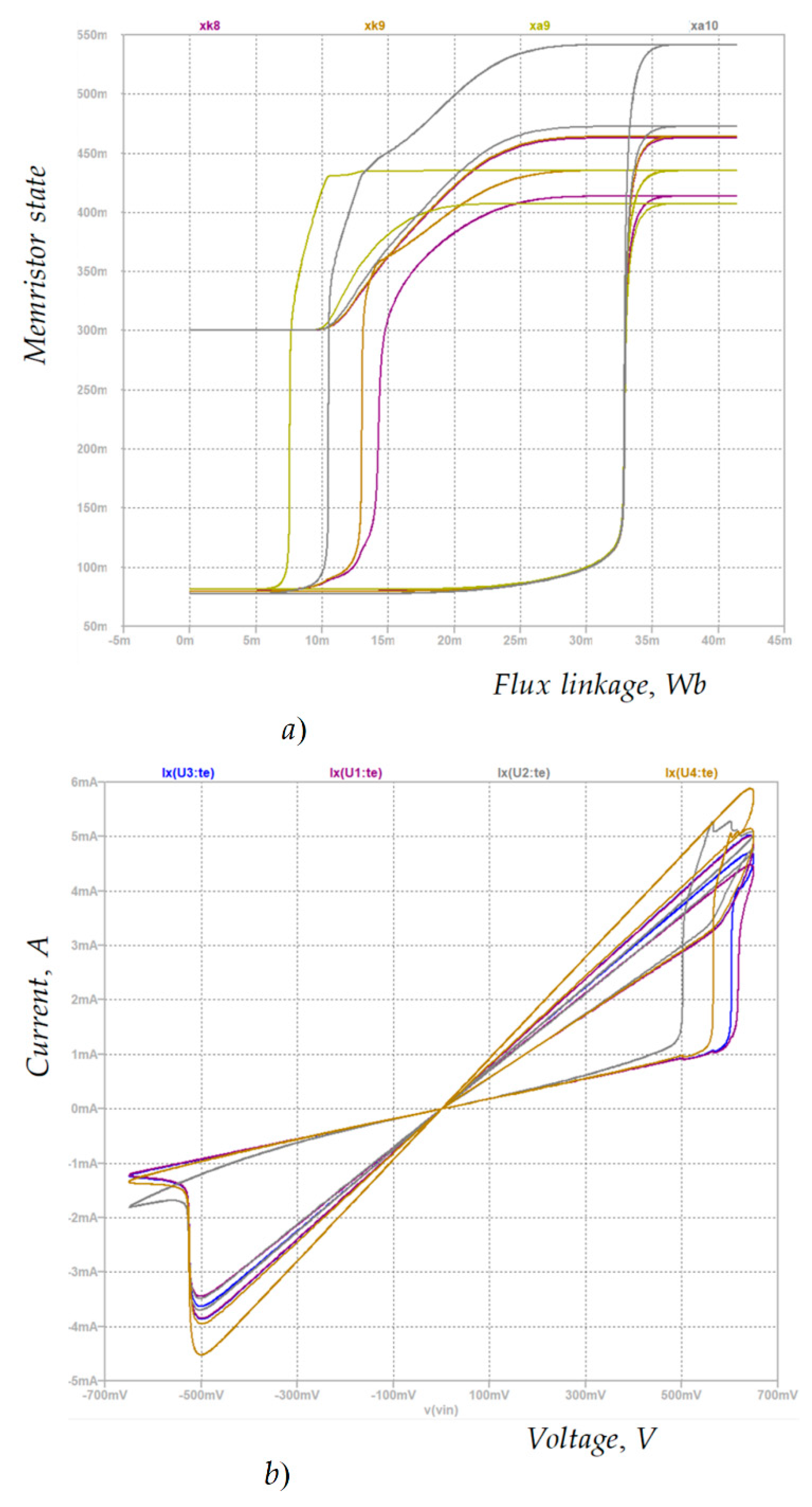
Figure 5.
(a) State–flux relationships of the standard tantalum oxide memristor models K8 and K9, and the modified models A9 and A10 with a sinusoidal voltage magnitude of 0.65 V and frequency of 5 Hz; (b) The corresponding current–voltage relationships of the considered tantalum oxide memristor models.

Figure 6.
Generalized LTSpice schematic of a memristor model.

Figure 7.
(a) A simple circuit for testing the memristor model in LTSPICE; (b) Time diagrams of the memristor voltage and state variable according to the tantalum oxide memristor models; (c) Corresponding current–voltage characteristics.
Figure 7.
(a) A simple circuit for testing the memristor model in LTSPICE; (b) Time diagrams of the memristor voltage and state variable according to the tantalum oxide memristor models; (c) Corresponding current–voltage characteristics.

Figure 8.
(a) Structure of a passive memristor crossbar; (b) A substituting equivalent electric circuit; (c) A schematic of the analyzed memory crossbar in LTSPICE.
Figure 8.
(a) Structure of a passive memristor crossbar; (b) A substituting equivalent electric circuit; (c) A schematic of the analyzed memory crossbar in LTSPICE.

Figure 9.
Time diagrams of memristor voltage and state variable derived during the process of writing, reading, and erasing information in the memristor memory crossbar.
Figure 9.
Time diagrams of memristor voltage and state variable derived during the process of writing, reading, and erasing information in the memristor memory crossbar.

Figure 10.
(a) Structure of a memristor neural network; (b) A schematic of a memristor-based synapse.
Figure 10.
(a) Structure of a memristor neural network; (b) A schematic of a memristor-based synapse.

Figure 11.
(a) Time diagrams of the input signals x1 and x2 for training the neural network; (b) Time diagrams of the input signals y1 and y2 for testing the neural net; (c) Time diagrams of the desired and the output signal of the neural network after testing and time diagram of the error signal expressed as a difference between the desired and the output signal of the feed-forward neural network; (d) A visualization of the minimizing of the mean square error over epochs.


Table 1.
A comparison of the considered existing and modified TiO2 memristor models.
| Criteria for Comparison | Titanium Dioxide Memristor Models | |||||||||
|---|---|---|---|---|---|---|---|---|---|---|
| - | K1 | K2 | K3 | K4 | K5 | A1 | A2 | A3 | A4 | A5 |
| Operating frequency | low | low | low | middle | low, middle, high | middle | middle | middle | middle | middle, high |
| Signal level | low, middle | low, middle | low, middle | low, middle | low, middle, high | low, middle | low, middle, high | low, middle, high | low, middle, high | low, middle, high |
| Nonlinearity | middle | middle | middle | middle | high | high | high | high | high | high |
| Accuracy | low | low | sufficient | sufficient | high | high | high | high | high | high |
| Activation thresholds | not applied | not applied | not applied | applied | not applied | applied | not applied | applied | applied | applied |
| Operating modes | soft-switching | soft-switching | soft and hard switching | soft and hard switching | soft and hard switching | soft and hard switching | soft and hard switching | soft and hard switching | soft and hard switching | soft and hard switching |
| Boundary effects | partially | partially | applied | applied | applied | applied | applied | applied | applied | partially |
| Nonlinear drift—voltage relationship | not applied | not applied | not applied | not applied | applied | applied | applied | applied | applied | applied |
| Tunability | low | partial | partial | partial | partial | applied | applied | applied | applied | applied |
| Complexity | low | low | low | middle | middle | middle | middle | middle | middle | middle |
| Application | analog and digital devices | analog and digital devices | analog and digital devices, NN | analog and digital devices, NN | analog and digital devices, NN, memories | analog and digital devices, NN | analog and digital devices, NN | analog and digital devices, NN | analog and digital devices, NN, memories | analog and digital devices, NN, memories |
Table 2.
Comparison of the considered existing and modified HfO2 memristor models.
| Criteria for Comparison | Hafnium Dioxide Memristor Models | ||||
|---|---|---|---|---|---|
| - | K6 | K7 | A6 | A7 | A8 |
| Operating frequency | low | low, middle | low, middle, high | low, middle, high | low, middle, high |
| Signal level | low | middle | low, middle, high | low, middle, high | low, middle, high |
| Nonlinearity | middle | high | high | high | high |
| Accuracy | low | middle | high | high | high |
| Activation thresholds | applied | applied | applied | applied | applied |
| Operating modes | soft switching | soft and hard switching | soft and hard switching | soft and hard switching | soft and hard switching |
| Boundary effects | not applied | applied | applied | applied | applied |
| Nonlinear drift—voltage relationship | not applied | not applied | partial | applied | applied |
| Tunability | partial | partial | applied | applied | applied |
| Complexity | middle | high | middle | middle | middle |
| Application | analogue and digital devices | analogue and digital devices, NN | analogue and digital devices, NN, memories | analogue and digital devices, NN, memories | analogue and digital devices, NN, memories |
Table 3.
Comparison of the considered existing and modified Ta2O5 memristor models.
| Criteria for Comparison | Tantalum Oxide Memristor Models | |||
|---|---|---|---|---|
| - | K8 | K9 | A9 | A10 |
| Operating frequency | low, middle, high | low, middle, high | low, middle, high | low, middle, high |
| Signal level | low, middle, high | low, middle, high | low, middle, high | low, middle, high |
| Nonlinearity | high | high | high | high |
| Accuracy | high | high | high | high |
| Activation thresholds | not applied | not applied | applied | applied |
| Operating modes | soft- and hard switching | soft- and hard switching | soft and hard switching | soft and hard switching |
| Boundary effects | partially | applied | applied | applied |
| Nonlinear drift—voltage relationship | applied | applied | applied | applied |
| Tunability | partial | applied | applied | applied |
| Complexity | high | high | middle | middle |
| Application | analogue and digital devices, NN, memories | analogue and digital devices, NN, memories | analogue and digital devices, NN, memories | analogue and digital devices, NN, memories |
Publisher’s Note: MDPI stays neutral with regard to jurisdictional claims in published maps and institutional affiliations. |
© 2021 by the author. Licensee MDPI, Basel, Switzerland. This article is an open access article distributed under the terms and conditions of the Creative Commons Attribution (CC BY) license (https://creativecommons.org/licenses/by/4.0/).
Share and Cite
MDPI and ACS Style
Mladenov, V. A Unified and Open LTSPICE Memristor Model Library. Electronics 2021, 10, 1594. https://doi.org/10.3390/electronics10131594
AMA Style
Mladenov V. A Unified and Open LTSPICE Memristor Model Library. Electronics. 2021; 10(13):1594. https://doi.org/10.3390/electronics10131594
Chicago/Turabian StyleMladenov, Valeri. 2021. "A Unified and Open LTSPICE Memristor Model Library" Electronics 10, no. 13: 1594. https://doi.org/10.3390/electronics10131594
Note that from the first issue of 2016, this journal uses article numbers instead of page numbers. See further details here.