1. Introduction
Memory signaling systems require high-density and high-speed signaling in high-performance computing systems in applications for artificial intelligence and big data management. In high-performance memory signaling systems, a printed circuit board (PCB) is needed to route a high number of signal channels between the chip and the dual in-line memory module (DIMM).
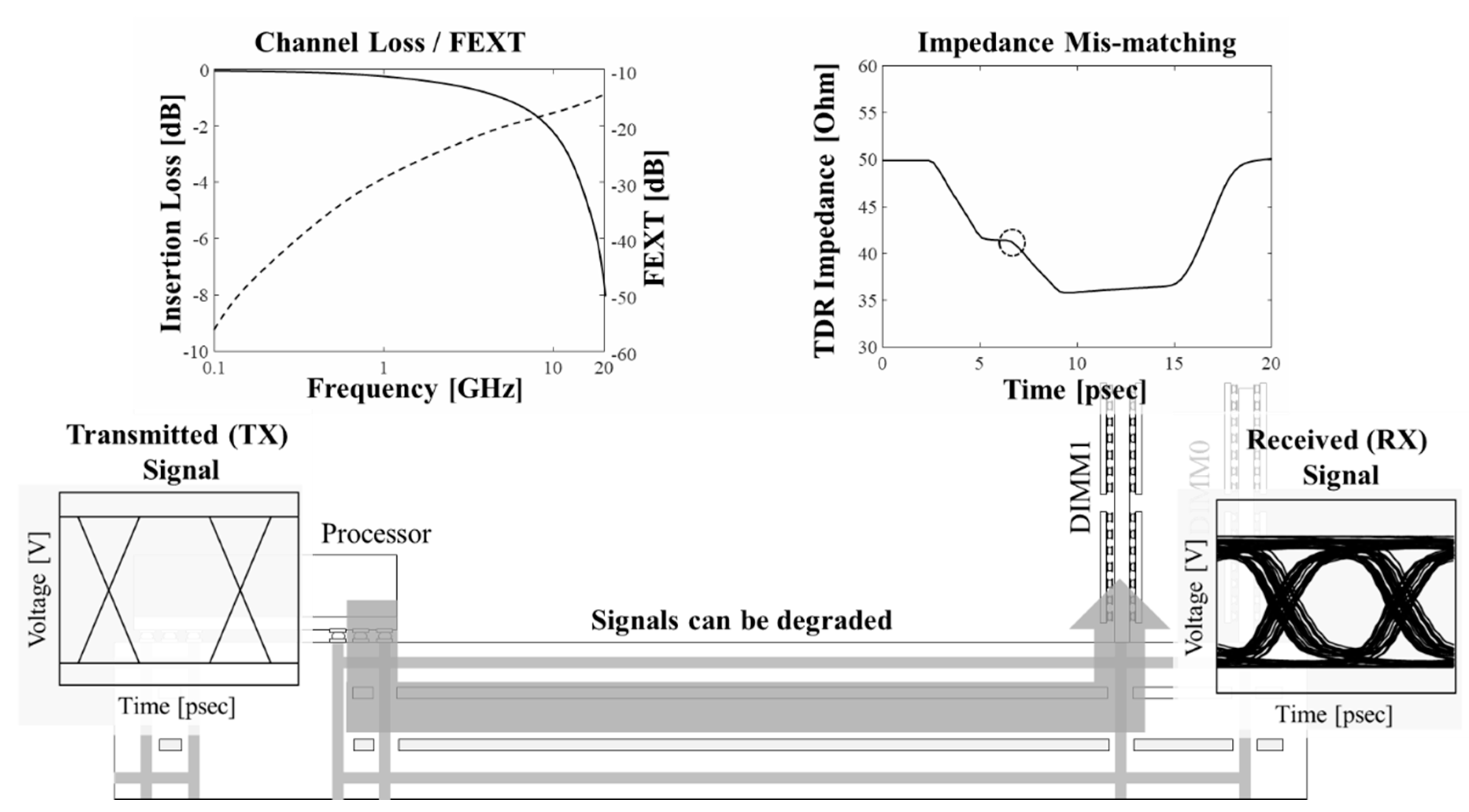
Figure 1 depicts a memory signaling system, including the central processing unit (CPU), PCB, and DIMM with major signal integrity (SI) design factors. To increase the speed of signaling in the memory system, it is necessary to reduce the time required by the high-speed signaling channel. Thus, to design high-speed signaling channels, the TDR impedance must be maintained at a constant value, while insertion loss and FEXT are minimized.
Within a limited space, the high density of the signaling channel causes unintentional signal degradation due to the increase in high-speed data transfer. The unintended interaction between signaling channels introduces crosstalk noise, which degrades the SI performance. In particular, FEXT is one of the dominant factors that degrades high-speed signaling channels. As a result, various attempts have been made to mitigate FEXT [
1,
2]. However, from an engineering perspective, the choice of mitigating FEXT by increasing the gap between channels or applying a new structure is not straightforward.
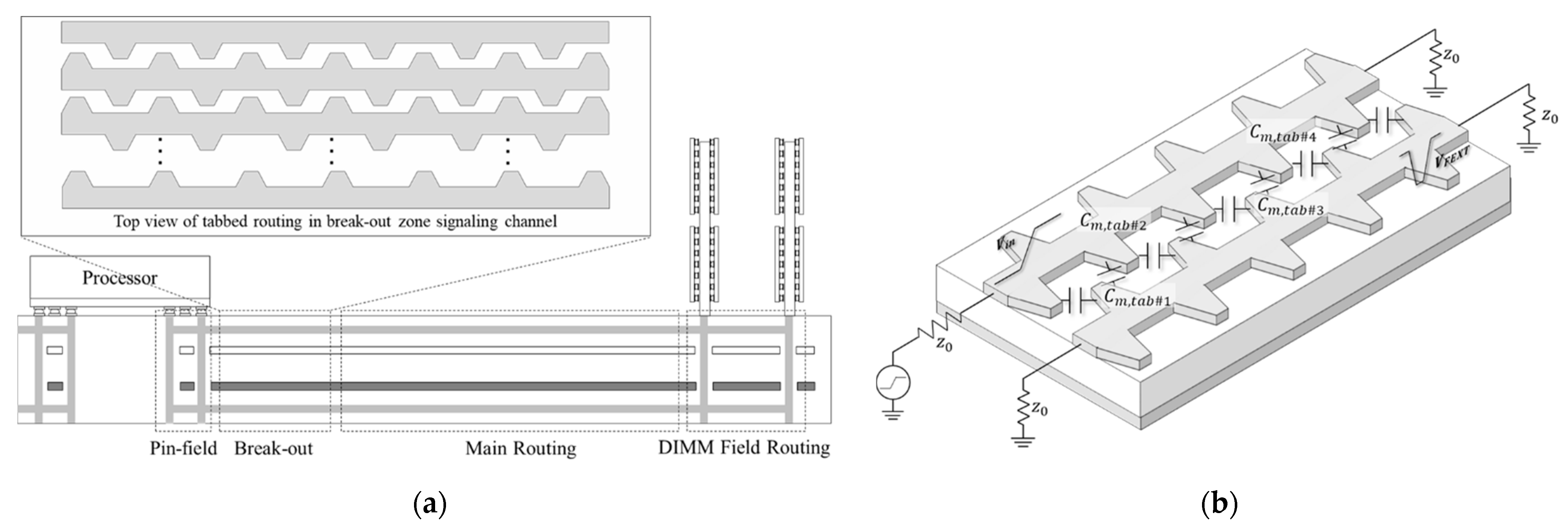
For these reasons, a new routing pattern, named tabbed routing, was proposed and applied to micro-strip lines of high-performance server PCBs by Intel Corporation [
3]. In general, when the CPU pins are out of the distributed pin field, the routing is performed using one bus consisting of eight DQ channels and two pairs of DQs, and the channels are routed with an even distance in the break-out zone. From the routing perspective, the routing from the CPU’s pin becomes wider as it goes to the DIMM package. Thus, at the break-out zone where the spacing is narrow between the signaling channels, a trapezoid-shaped tab is added to the general signaling trace for tabbed routing, as shown in
Figure 2a,b.
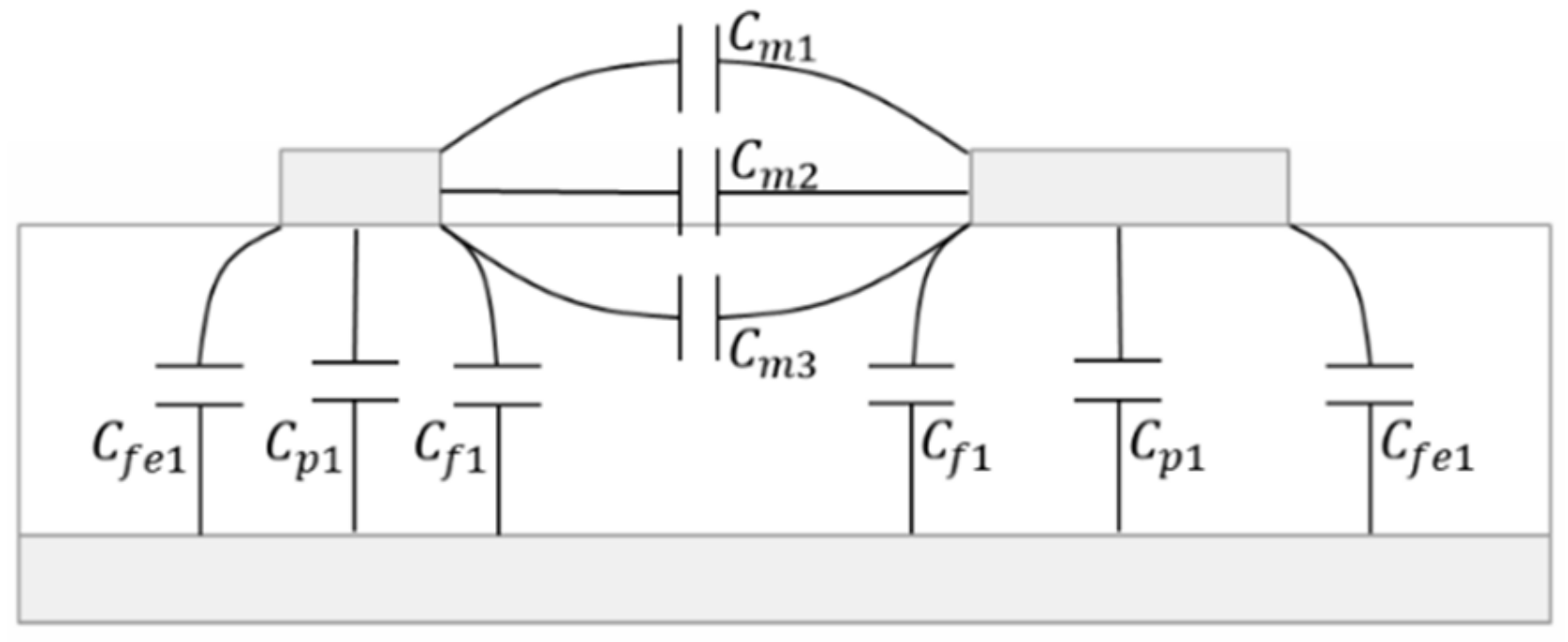
As shown in
Figure 2b, unlike a general micro-strip channel, an additional mutual capacitance,
, is formed between the tab and the adjacent channel. The FEXT voltage is determined between the ratio of mutual- and self-capacitance, and the ratio of mutual- and self-inductance, as shown in Equation (1) below [
3].
However, not only is additionally generated by tabs, but it also affects the mutual- and self-inductance and capacitance values of the channels. Furthermore, because the width and space of tabbed routing are not constant, it is a challenge to undertake modeling-based design and optimization that can minimize insertion loss and FEXT excluding 3D EM simulation and measurement.
In [
4], a generalized equation-based tabbed routing model is proposed using the segmentation method with an asymmetrical coupled micro-strip line. The self- and mutual-capacitance is calculated based on the asymmetrical micro-strip line, and self- and mutual-inductance can be obtained from the calculated capacitance values. However, the self- and mutual-inductance values are affected by
. Due to this difference in self- and mutual-inductance, the consistency of the tabbed routing model is degraded. Thus, to increase the accuracy of tabbed routing in relation to SI, a tabbed routing model based on more accurate inductance and capacitance values is needed.
In this paper, we propose improved modeling of tabbed routing using an asymmetrical coupled micro-strip line using the segmentation method. The calculation of the inductance is performed by considering the effect of the tab fringing capacitance value, thus improving the consistency of the overall inductance value in
Section 2. In
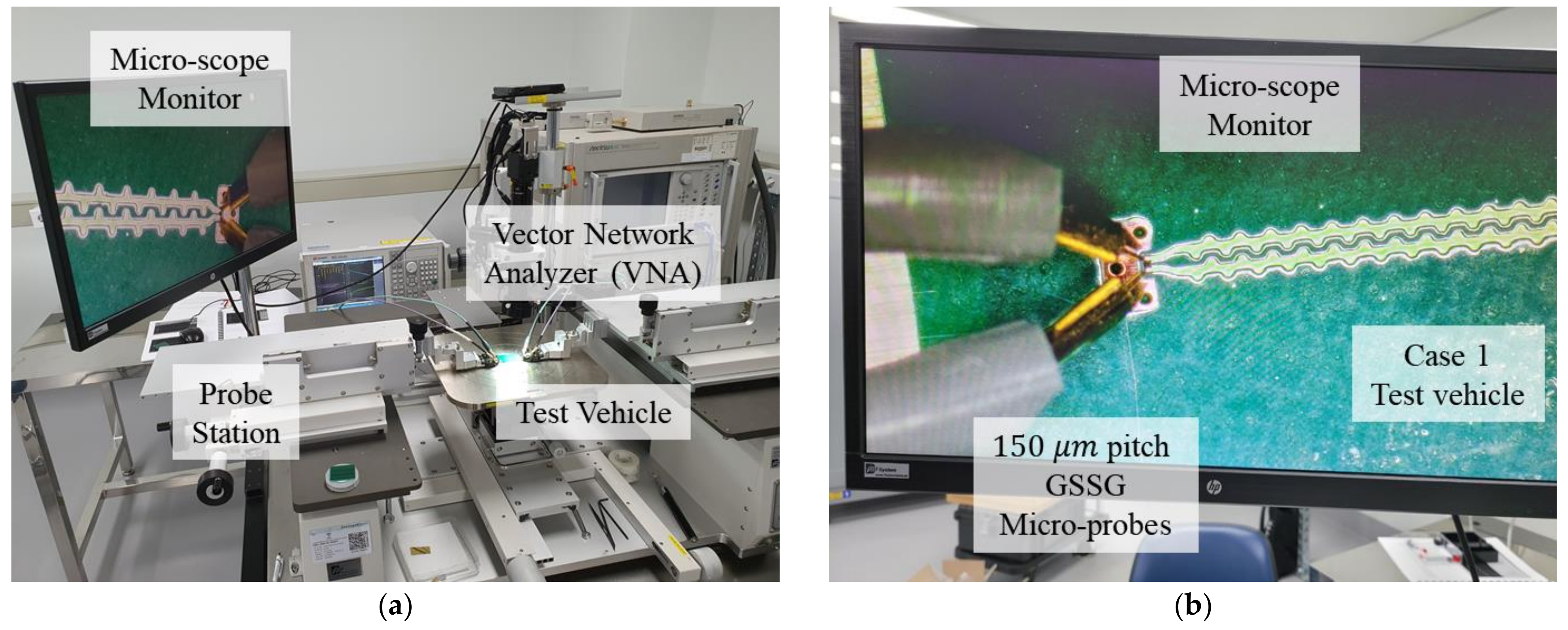
Section 3, for verification of the proposed modeling method, the manufactured PCB patterns and measurement set-up are shown.
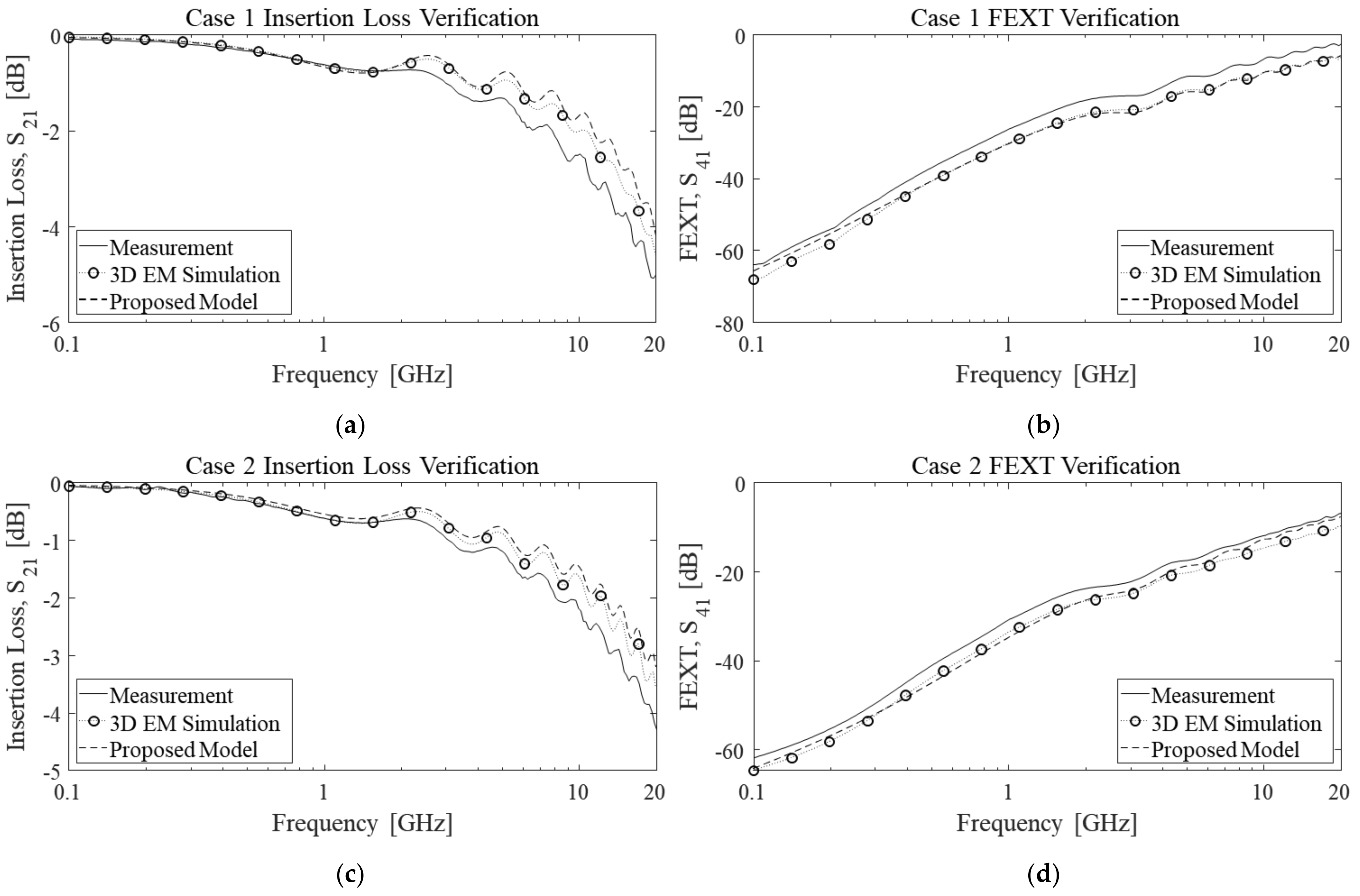
The proposed tabbed routing model was verified by comparison of the insertion loss and FEXT for two tabbed routing designs, using 3D EM simulation and measurement results up to 20 GHz in the frequency domain. The proposed tabbed routing model was compared with the previous model in terms of insertion loss, FEXT, and self-impedance in frequency domain. In
Section 4, we analyze the tabbed routing in terms of insertion loss, FEXT, self-impedance of
Z11 in the frequency domain, and TDT and FEXT in the time domain, with and without tabbed routing. Furthermore, tabbed routing with design variations was compared and analyzed. Finally, we discuss the application of the high-speed signaling channel with tabbed routing to high-performance computing systems from the perspective of signal integrity. This SI perspective allows intuitive analysis of tabbed routing.
2. Modeling of High-Speed Signaling Channel with Tabbed Routing
In this section, we introduce the signal integrity model and modeling procedure of the high-speed signaling channel with tabbed routing.
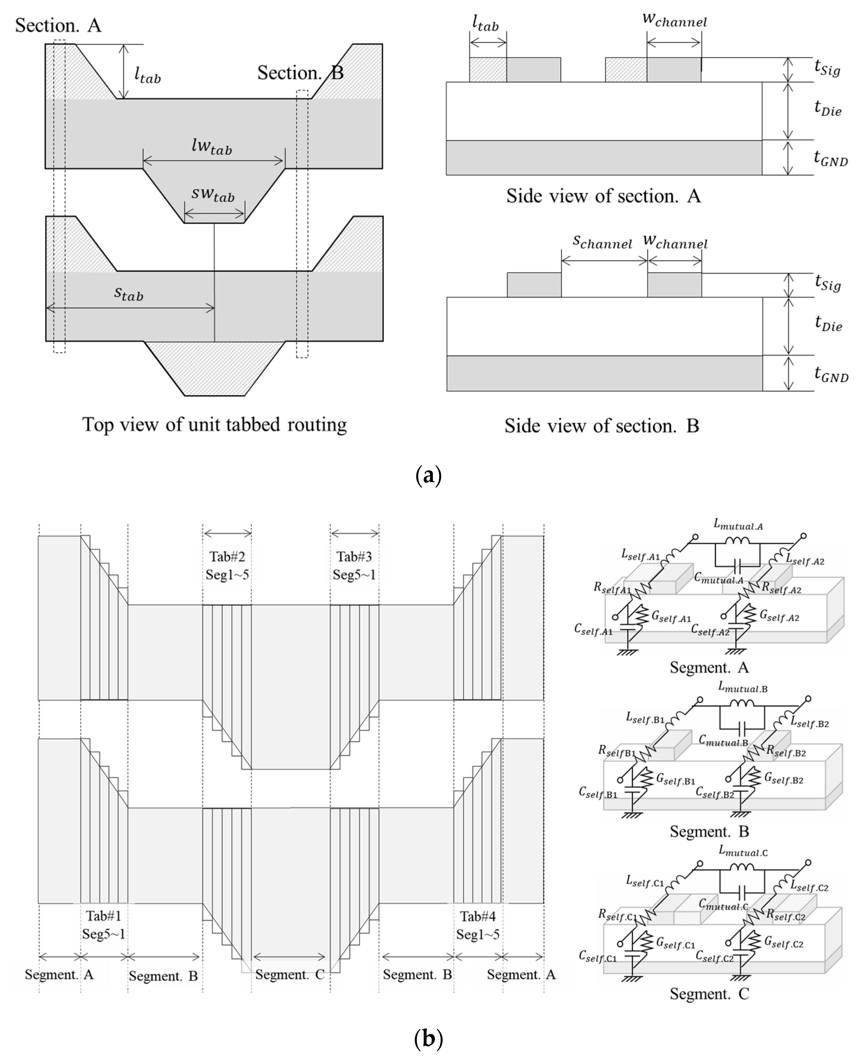
Table 1 shows the structural parameters and definitions.
Figure 3a shows the top and side views of one-unit tabbed routing. To aid understanding of the tabbed routing model, we illustrate one-unit tabbed routing in
Figure 3a. In the segment A and B of
Figure 3b, the channel width can differ due to the tab design parameters.
In the general micro-strip line structure, the characteristics of signaling trace, namely, insertion loss, FEXT, TDR, are determined by the dimension of the micro-strip line. Due to the non-uniform dimensions of the tabbed routing, the E- and H-fields are also non-uniformly formed through the signaling channel. Thus, it is difficult to analyze tabbed routing compared to the general micro-strip line. For this reason, reference [
4] proposed modeling of tabbed routing using a segmentation method, as shown in
Figure 3b. In reference [
4], the capacitance and inductance were calculated for an asymmetrical coupled micro-strip line depending on the width and space change. In addition, for the fringing effect that occurs between tabs, an additional fringing capacitance was calculated and applied to the equivalent circuit model.
However, the inductance matrix values were calculated in a homogenous medium based on the capacitance value for a two-coupled asymmetrical micro-strip line, which occurs in the cross-section without reflecting the tab fringing effect [
4].
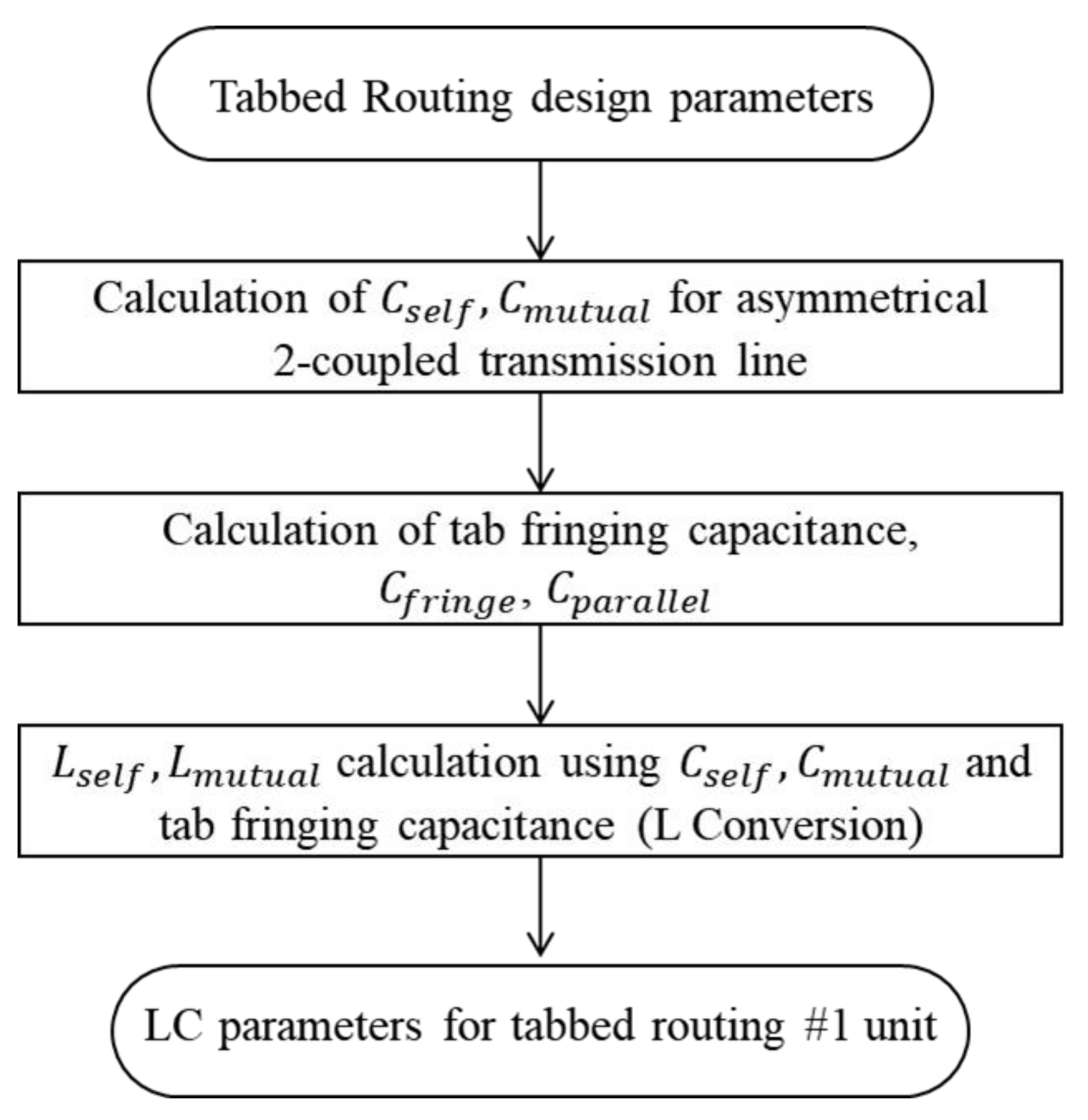
Thus, in this paper, we proposed an improved modeling method, which can apply the tab fringing effect to the inductance value as shown in
Figure 4. The proposed tabbed routing modeling method is constructed using the segmentation method, similar to that of reference [
4]. First, the self- and mutual-capacitance values of the asymmetrical coupled micro-strip line are calculated using the equation of reference [
4] from the fixed tabbed routing physical design parameters, as shown in
Table 1.
In Second, we calculate the fringing capacitance,
, using the fixed physical design parameters of tabbed routing. In the next step, unlike the calculation of self-and mutual-capacitance and inductance undertaken in ref. [
4], the self- and mutual-inductance values are calculated through matrix calculation using the calculated self- and mutual-capacitance calculation results and fringing capacitance results. In this paper, we defined “L conversion” as an inductance matrix calculation that considers mutual-capacitance and tab fringing capacitance. Using the calculated inductance and capacitance values with resistance, and the conductance parameters, a one-unit tabbed routing model can be constructed. A detailed explanation of each step of the modeling procedure is provided in the next section.
The design parameters and definition are defined in
Table 1 and
Figure 3a. To obtain the total capacitance matrix, the partial capacitance parameters are illustrated in
Figure 5.
The capacitance matrix
C for the two-coupled micro-strip line is:
The C matrix, Equation (2), is the frequency independent value, where , , represent the self-capacitance values of line 1 and line 2 to ground, and mutual capacitance between line 1 and line 2, respectively.
Each capacitance value is formulated by Equations (3)–(5). From the design parameters, each capacitance value of the asymmetrical micro-strip line can be calculated using the equations from reference [
5].
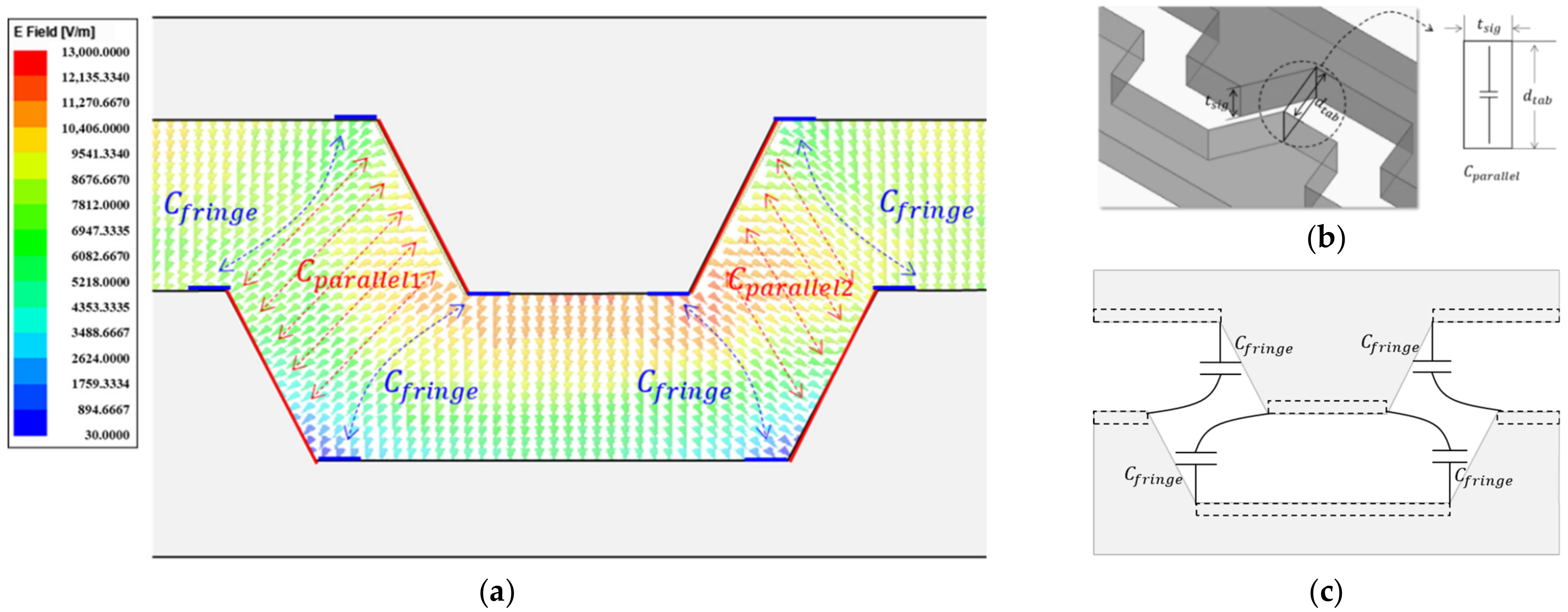
The tab fringing capacitance is calculated in the second step. In contrast to normal micro-strip lines, there is an additional tab fringing mutual-capacitance between tabs. The E-field distribution result of tabbed routing is plotted in
Figure 6a. In general, the E-field vector of the micro-strip line is generated in the direction perpendicular to the direction of the electromagnetic wave. However, due to the tab, the E-field vector is distributed differently, as shown in
Figure 6a. It is shown that the E-field distribution is divided into an oblique tab and the edge of the Table Fringing capacitance modeling is performed through the field for each part, as shown in
Figure 6b,c [
4].
Figure 6b introduces two different fringing capacitance models according to the distribution of the E-field [
4]. First, for the oblique slope, the parallel surfaces face each other, and
can be calculated using Equation (6):
Next, as shown in
Figure 6c, the fringing capacitance,
, is introduced via Equations (8)–(10) [
4]:
In this paper, Equations (6)–(10) were applied to calculations based on air, the medium in which the E-field is distributed between the two-coupled micro-strip line without passivation. In addition, the proposed model is considered in an ideal micro-strip line, and the PCB etching effect is not considered. By applying the additional mutual capacitance,
and
, between adjacent tabs, the oblique E-field that is caused by the tabs can be approximately considered. Using the two steps mentioned above, the modeling of tabbed routing reflecting the tab effect can be undertaken. However, to increase the consistency of the modeling method, we propose and introduce an additional step. The inductance matrix of the two-coupled asymmetrical micro-strip line,
L, can be calculated using Equation (11):
Due to velocity splitting in the propagation model in non-homogeneous media [
5], the inductance matrix,
L, can be obtained using
, which is calculated by converting the dielectric material to air, where
is the wave velocity and
is the
identity matrix. However, the inductance calculation using Equation (11) cannot reflect the fringing capacitance value calculated in step 2.
From the perspective of the equivalent circuit model of tabbed routing,
and
can be considered to be connected to each segment in series with mutual-capacitance as the half-value. Thus, the inductance at tab segments 2, 3, and 4, which are connected with
, can be calculated using Equation (12):
For the edge of the tab, the inductance at tab segments 1 and 5, which are connected with
, can be calculated using Equation (13):
Using these three inductance calculation equations, a tabbed routing model can be configured, in which the inductance and capacitance models considering tab fringing capacitance is applied. To verify the proposed modeling and to compare results with the previous model [
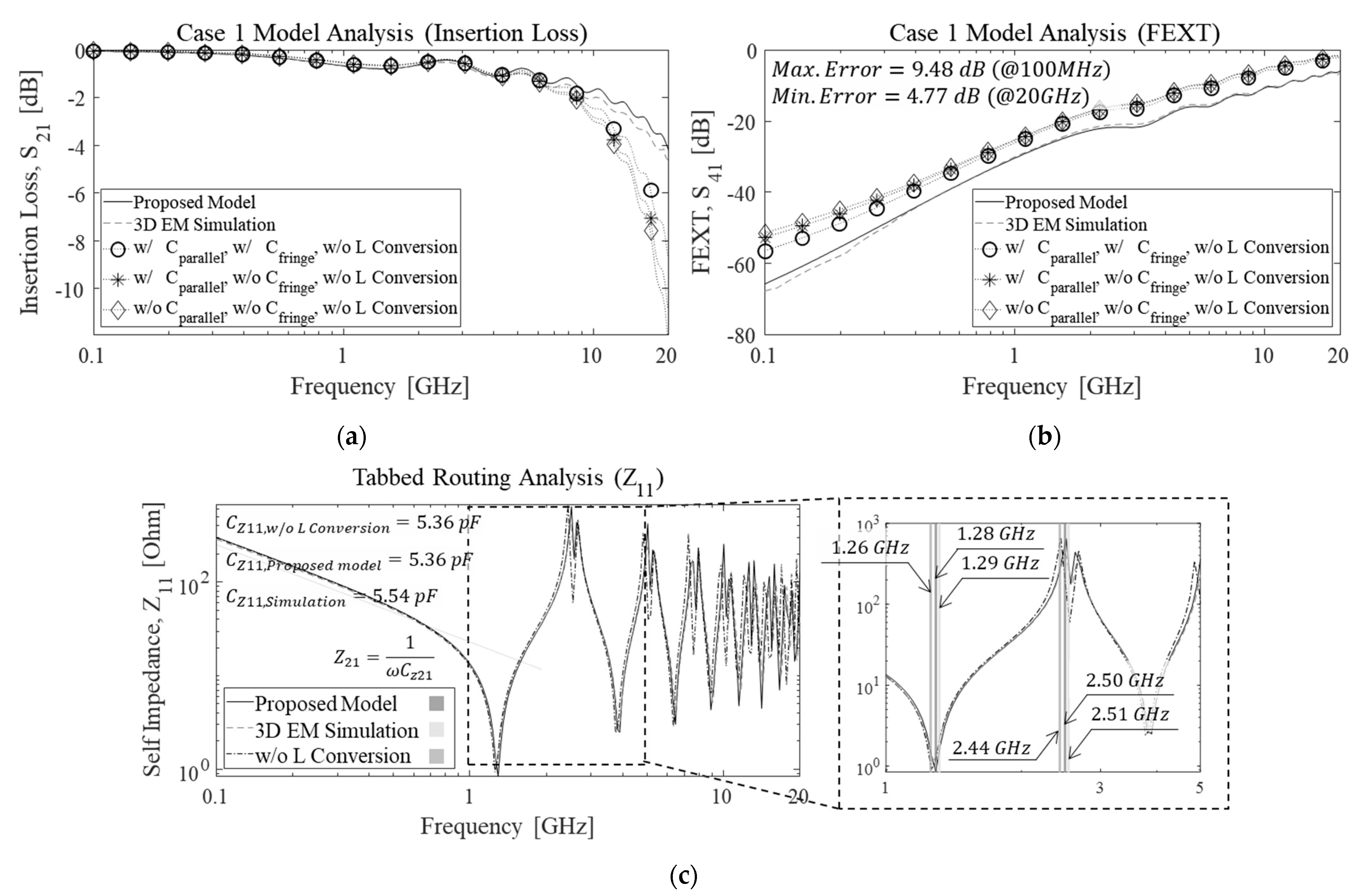
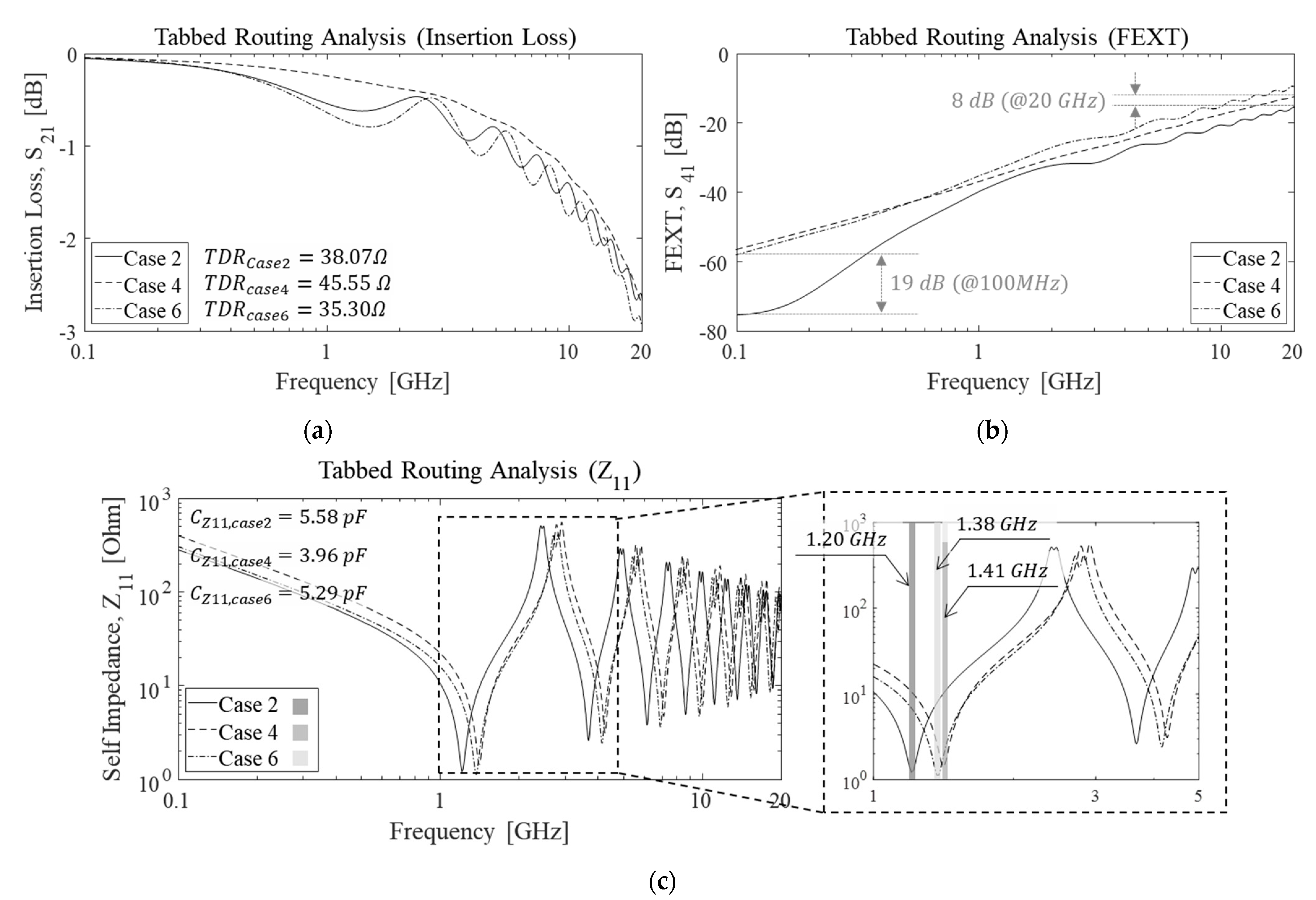
4] without the L conversion effect, the insertion loss and FEXT results were obtained using the proposed model. These results are compared using measurement and 3D EM simulation in the frequency domain in the following section.
5. Conclusions
As the demand for high-performance computing systems increases, high-speed signaling channels should be designed in the high-frequency range with degraded loss for reliable data transmission. A high-speed signaling channel with tabbed routing has an advantage in terms of signal integrity while degrading the coupling between channels.
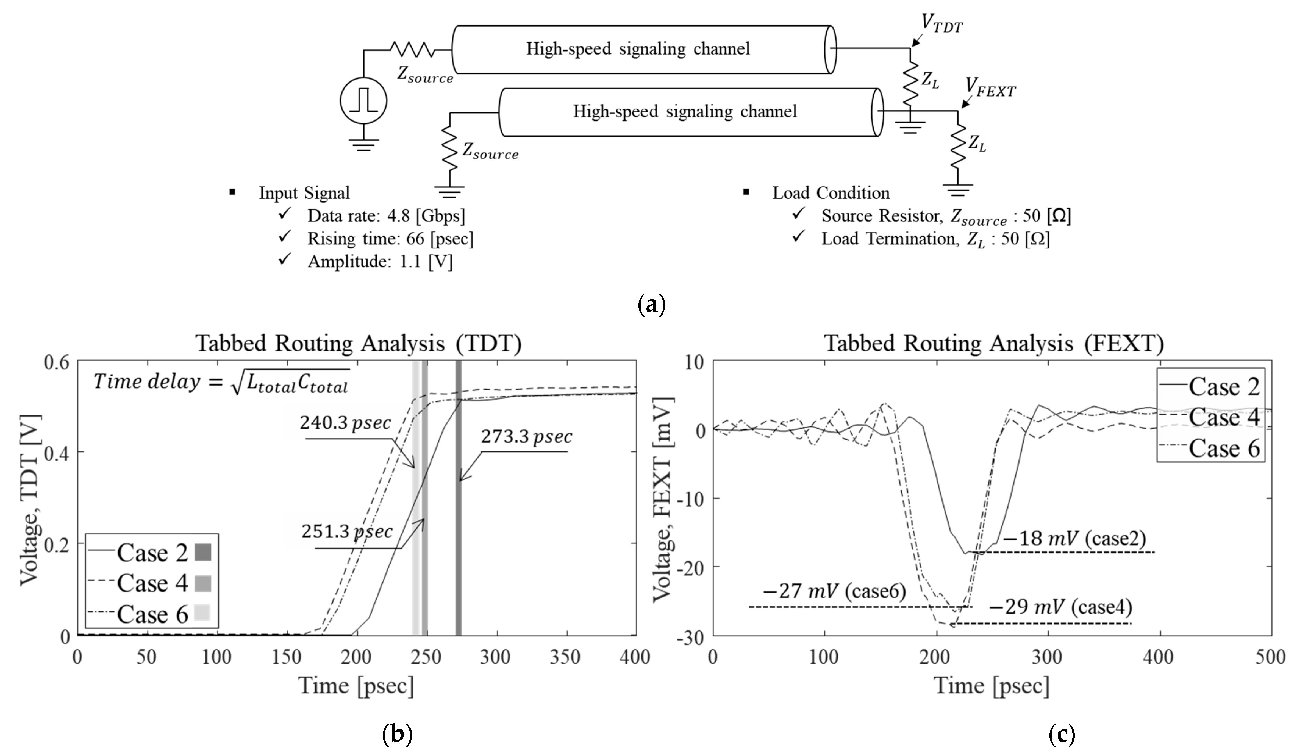
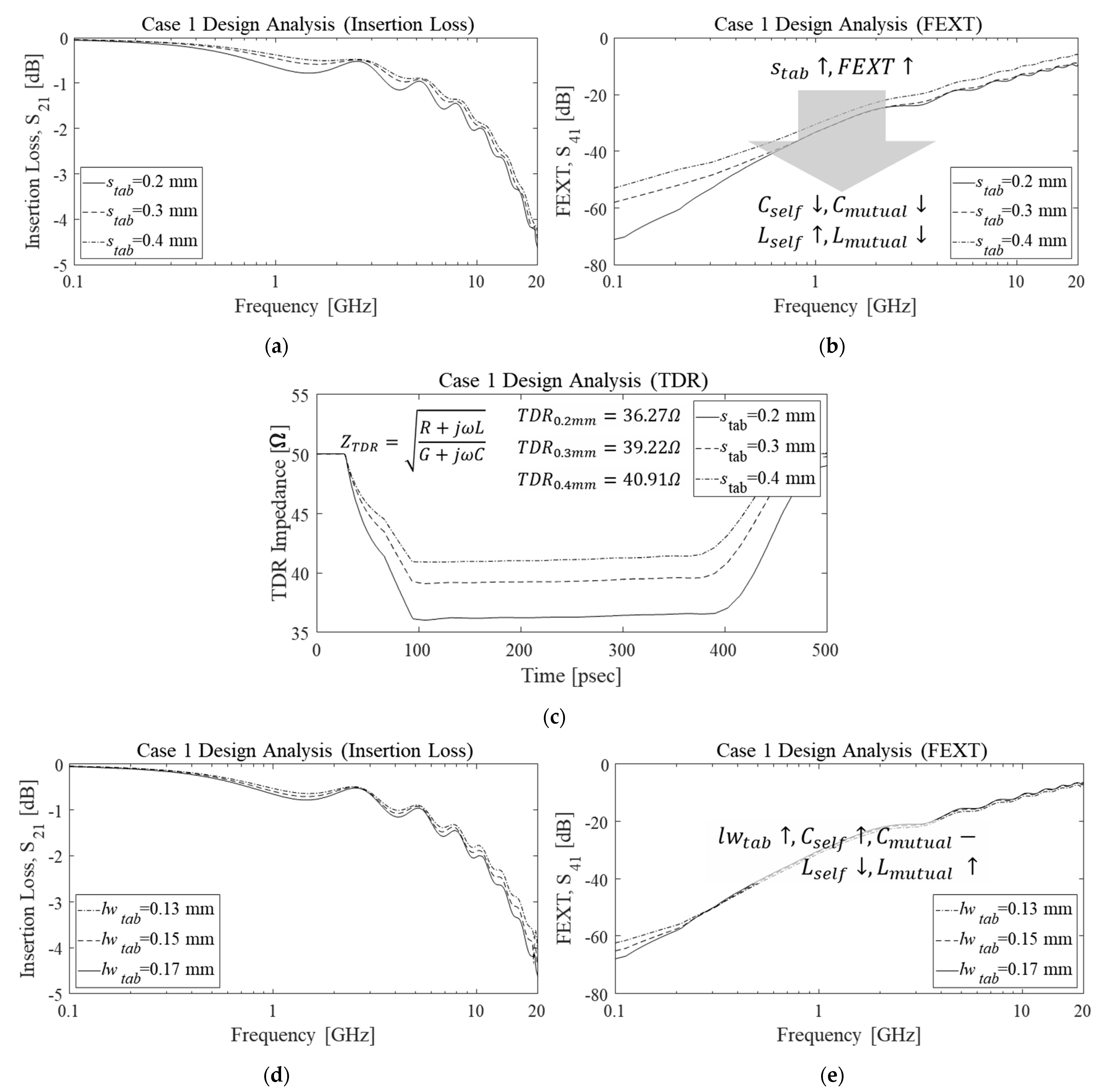
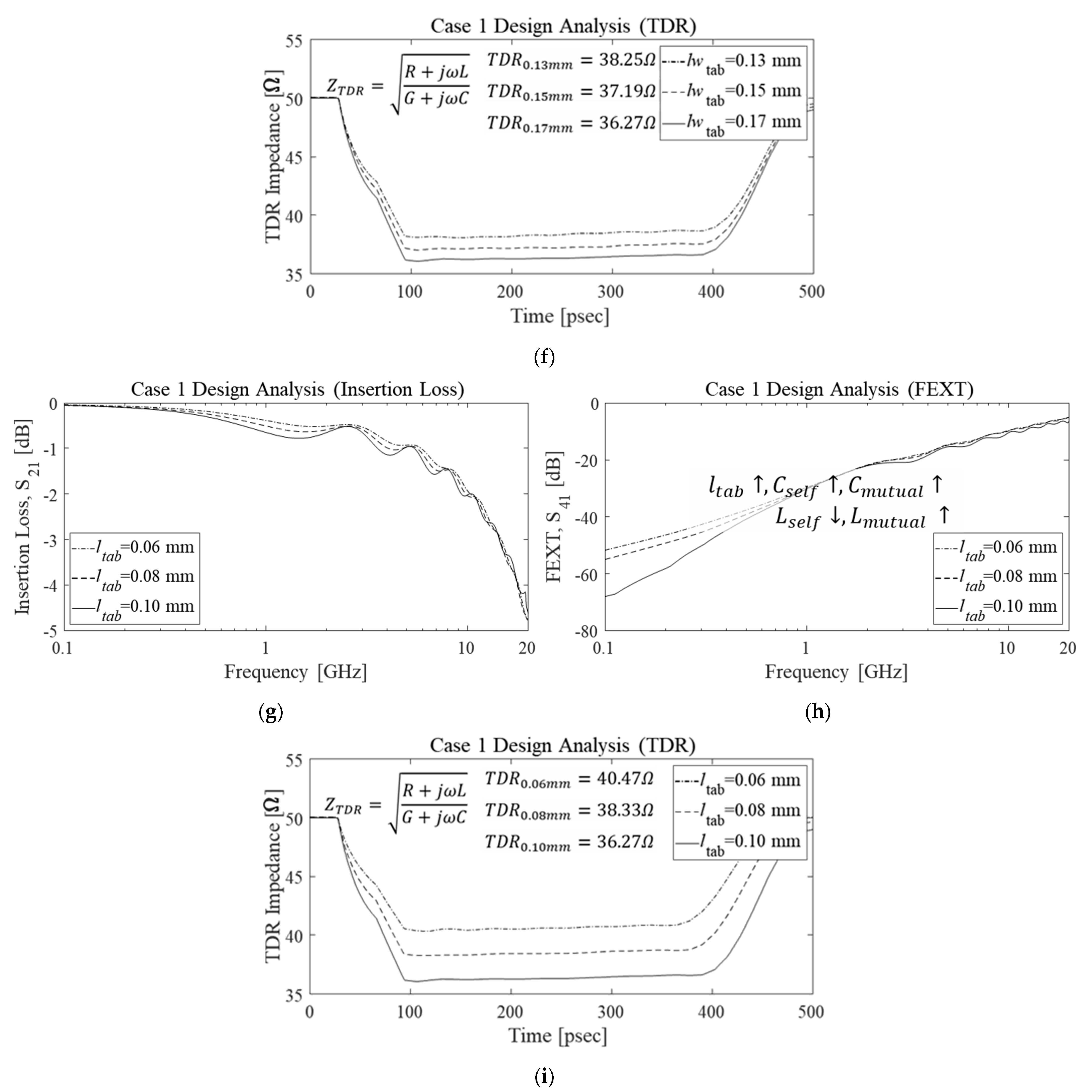
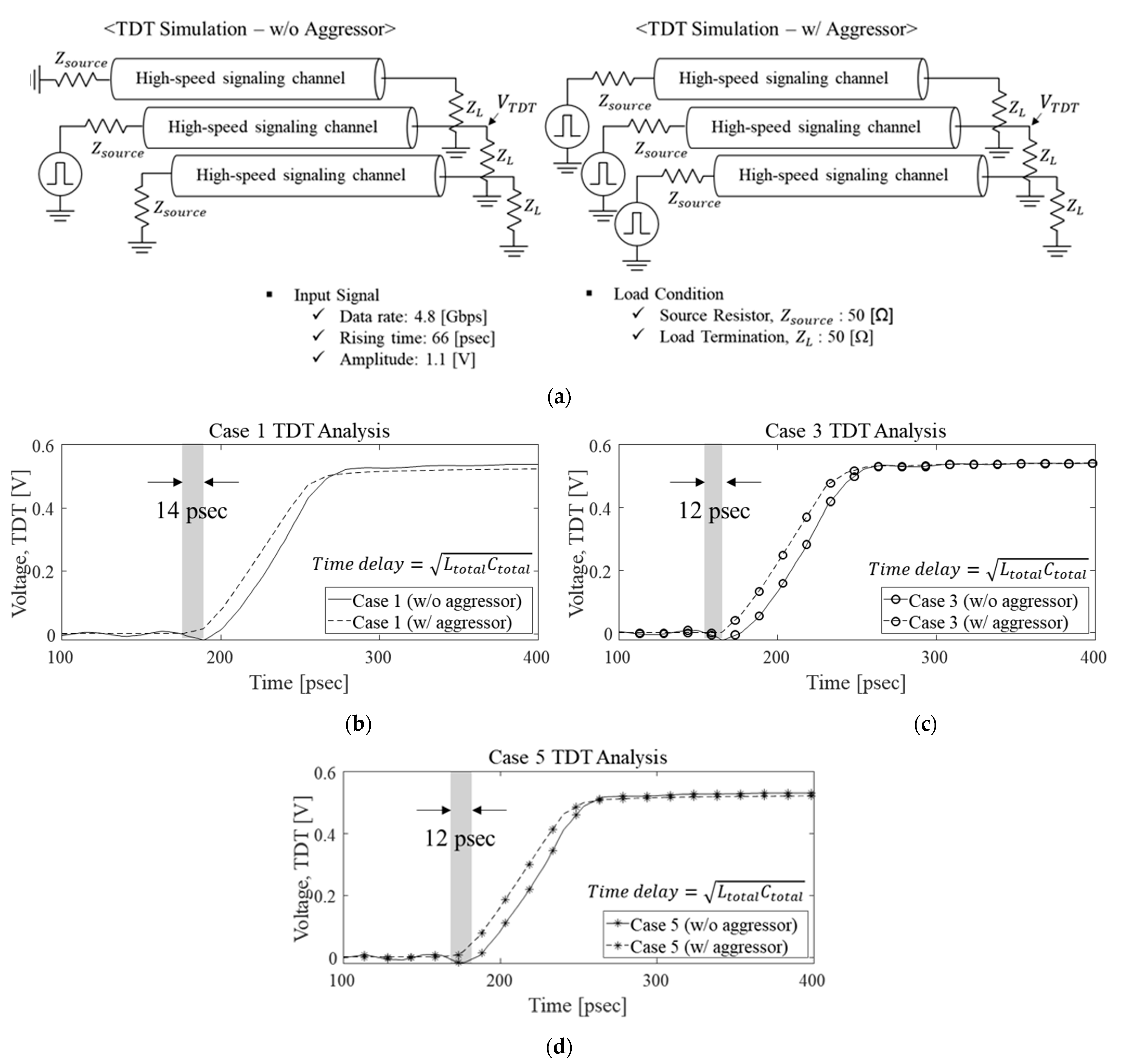
In this paper, we proposed and verified a tabbed routing model with an improved equivalent self- and mutual-inductance model that considers tab fringing capacitance. In frequency domain verification, we compared the insertion loss and FEXT of VNA measurement using manufactured PCBs with different tab designs. From the comparison of the measurements and 3D EM simulation, the proposed model was successfully verified in the frequency domain. In addition, the proposed model was compared with the previous tabbed routing model in the frequency domain. The effect on the L conversion proposed in this paper was shown in terms of the insertion loss, FEXT, and self-impedance of Z11. In addition, we showed that the insertion loss, FEXT, and self-impedance of the proposed model match better than those of the previous model. After verification, using the proposed model we analyzed the signal integrity of high-speed signaling channels with and without tabs in the frequency and time domains. Tabbed routing was investigated using inductance and capacitance parameter analysis; results showed that FEXT degraded when tabs were applied to channels with the same space. Tabbed routing analysis also showed that tabbed routing has a larger value of mutual capacitance than that of the channel without tabs due to the increase in the facing area between channels. Furthermore, tabbed routing not only has the advantage of degrading FEXT, but also controls the TDR impedance and time delay without changing the width or space of the channel within a defined area. Using the proposed model, we also analyzed tabbed routing based on the variation of three design parameters in the frequency domain.


 ,
, 


