Article

Helium Metastable Distributions and Their Effect on the Uniformity of Hydrogenated Amorphous Silicon Depositions in He/SiH4 Capacitively Coupled Plasmas

1
Department of Mechanical Engineering, Gachon University, Seongnam 13120, Korea
2
Department of Mechanical Engineering, Hanyang University, 55 Hanyangdaehak-ro, Sangnok-gu, Ansan 15588, Korea
*
Authors to whom correspondence should be addressed.
Coatings 2022, 12(9), 1342; https://doi.org/10.3390/coatings12091342
Submission received: 29 July 2022 / Revised: 17 August 2022 / Accepted: 7 September 2022 / Published: 15 September 2022
(This article belongs to the Special Issue New Advances in Plasma Deposition and Its Applications)

Abstract

:
This study investigates, numerically, the spatial distribution of metastable helium (He*) in He/SiH4 capacitively coupled plasma (CCP) for the purpose of optimizing plasma density distributions. As a first step, we presented the results of a two-dimensional fluid model of He discharges, followed by those of He/SiH4 discharges to deposit hydrogenated amorphous silicon films, to investigate which factor dominates the coating uniformity. We retained our CCPs in the 300 mm wafer reactor used by the semiconductor industry in the recent past. Selected parameters, such as a sidewall gap (radial distance between the electrode edge and the sidewall), electrical condition of the sidewall, and position of the powered electrode, were considered. In addition, by increasing the gas pressure while varying the sidewall condition, we observed modification of the plasma distributions and, thus, the deposition rate profiles. According to the results, the shift in He* distributions was mainly due to the reduction in the electron mean free path under conditions of gas pressure higher than 100 Pa, as well as local perturbations in the ambipolar electric field due to the finite electrode structure. Small additions of SiH4 largely changed the He* density profile in the midplane of the discharge due to He* quenching. Furthermore, we found that the wide sidewall gap did not improve deposition uniformity against the expectation. This was because the excitation and ionization rate profiles were enhanced and localized only near the bottom electrode edge.

1. Introduction

The rise of technologies, such as big data, the Internet of Things, and smartphones, is generating enormous amounts of data [1]. In the 4th Industrial Revolution, for example, high-end storage devices, such as recent flash memory chips, have become essential [2]. As a result, thin-film deposition technology has demonstrated substantial progress with regard to its attributes for the development of state-of-the-art memory chips. Moreover, plasma deposition technologies, such as plasma-enhanced chemical vapor deposition (PECVD) and plasma-enhanced atomic layer deposition (PEALD), offer the possibility of uniformly growing these films at high deposition rates [3,4,5].
In any case, plasma deposition involves an extremely complex process that is not easy to analyze, largely because the results of this process might be sensitively influenced by a large number of parameters [6,7]. Despite the physical and chemical complexity of plasma deposition not being fully resolved, the size of semiconductor devices continues to shrink, necessitating an adherence to specific requirements, including an extremely high degree of uniformity [8,9]. Additionally, industrial applications require the ability to repeat processes and the reactor size should be small to reduce cost [10]. Thus, the use of plasma-enhanced chemical vapor deposition (PECVD) using capacitively coupled plasma (CCP) is often chosen for coating thin films at a satisfactory level of uniformity.
In microelectronics fabrication, CCP PECVD with noble-gas-based mixtures (such as He/SiH4, Ar/SiH4, and Xe/SiH4) has been used for thin-film deposition [11]. Even though the metastable species of the noble gases dominate the ionization processes, experiments in these devices have shown highly non-uniform distributions of excited atomic and molecular states. For example, McMillin and Zachariah presented results from their experiments in the Gaseous Electronics Conference reference cell (GECRC), demonstrating that excited state species vary with gas mixtures, gas pressures, and applied voltages [12,13]. The researchers studied the density profiles of excited state argon [Ar(4s)] in Ar, Ar/O2, Ar/CF4, and Ar/Cl2 plasmas by using laser-induced florescence (LIF). Interestingly, McMillin and Zachariah demonstrated that a small amount of electron-attaching gases, such as O2 and CF4, can significantly change the Ar* profile in Ar/O2 and Ar/CF4 discharges [13]. Metastable species’ roles in CCPs remain extensively investigated in recent reports [14,15,16]. In a particle-in-cell simulation, Wen et al. investigated electron elastic scattering and plasma density profile transition by incorporating metastable atoms [16].
Various types of gas mixtures have been considered, but in many cases, it has been said that a larger electrode or a larger reactor may be helpful in improving uniformity. The feasibility resides in the fact that one can induce spatial changes of electric fields that are found away from wafer edges. However, increasing the electrode size of a reactor can result in a rising reactor price. Additionally, the enlarged reactor will take up more space on the semiconductor manufacturing line. While this is being accomplished, it is still difficult to achieve uniformity in the electrode edge deposition rate profile [17,18,19,20]. By proceeding radially outward from the electrode edge, the geometric configuration of the reactor produces significant variations in various physical aspects, including discharge structure, gas flow, and source gas distribution. Radial profiles of the radical fluxes towards an electrode’s surface are affected by these features, resulting in non-uniform profiles of the edge thickness profiles. Several previous studies have observed and discussed this technical problem [20,21].
Considering this study’s novelty, compared to our previous studies, we used different reactor geometries in this study. Top electrodes are directly connected to sidewalls, for example. As a result, we can more clearly observe the electrode edge effects caused by excited species because there is only one corner point of the electrode edge. Additionally, the distance between the bottom electrode and the sidewall was altered, which allows us to observe electrode edge effects under a variety of conditions. Further, one of the reactor geometries is similar to the GECRC, so our metastable species distribution results can be compared with those from previous experiments and numerical simulations. Finally, due to the different geometry, different apparatus was used for experimental measurements. In addition, despite its physical importance, prior systematic studies of the metastable species distributions on plasma uniformity used simple chemistry or applied plasma for etching (for example, Ar/CF4 or Ar/Cl2). Therefore, a thorough understanding of how metastable species distributions affect plasma uniformity in practical gas mixture deposition reactors is crucial. Specifically, we examine how metastable species distributions impact the plasma uniformity in practical CCP PECVD. The objective of this study was, therefore, to numerically investigate the spatial distributions of metastable helium species (He*) in He/SiH4 capacitively coupled plasmas (CCPs) to understand how these plasma density distributions might be optimized.
The results of a two-dimensional fluid model of He discharges are first described, followed by those of He/SiH4 discharges to deposit hydrogenated amorphous silicon films. We examined which factor is most important to achieve uniform coatings. We retained our CCPs in the 300 mm wafer reactor used by the semiconductor industry in the recent past. We considered design parameters, such as a sidewall gap (radial distance between the electrode edge and the sidewall), electrical condition of the sidewall, and position of the powered electrode. In addition, by increasing the gas pressure while varying the sidewall condition, we observed changes in the plasma distributions and, thus, the deposition rate profiles.
We briefly describe our computational model in Section 2, present and discuss our results in detail in Section 3, and provide our conclusions in Section 4.

2. Materials and Methods

2.1. Governing Equations

The governing equations in the self-consistent CCP model are described in our previous publications [22,23,24]. For brevity, we only provide a brief description of them here. Solving the following equations accounts for the electron energy balance:
n e ε t + 5 3 n e ε v e 5 3 n e D e ε = S ε .
Here, ne, ε, t, ve, De, and Sε are the electron density, the electron energy, the time, the electron velocity, the electron diffusion coefficient, and the source of the electron energy, respectively. The electron energy source, Sε, in Equation (1) is given by:
S ε = e J e E n e i m s r ε r k r , i N i .
Here, −e, Je, E, kr,i, and Ni are the charge of an electron, the electron flux, the electric field, the rate coefficient of the rth reaction with the ith species, and the density of the ith species, respectively. Further, ms is the number of species involved in this reaction and εr represents the threshold energy in an inelastic collision or the mean electron energy loss in an elastic collision.

2.2. Numerical Methods

Using the commercial multi-physics software CFD-ACE+ (version 2020.5), we simulated the capacitively coupled SiH4/He plasma using a 2D fluid model [25]. A number of previous studies have successfully used CFD-ACE+ to simulate discharge cases, including both low-pressure inductively coupled plasmas and atmospheric pressure capacitively coupled plasmas [26,27,28].
By using the Scharfetter–Gummel exponential scheme, we discretized the electron density conservation equation and the electron energy balance equation. By using the kinetic module integrated in CFD-ACE+, the electron energy distribution function (EEDF), which calculates electron impact reaction rate coefficients, electron mobility, and electron diffusivity, was calculated a priori. To reduce computational costs, the 0D Boltzmann equation was solved for the EEDF. A lookup table was generated by solving the 0D Boltzmann equation as a preprocessor step. In Kolobov and Arslanbekov, details about solving the Boltzmann equation are provided [26].
As a result of the small integration time step that should be used for our CCP model, resolving all balances simultaneously will incur a high computational cost. This bottleneck was overcome by adopting a multi-time-scale framework that separated the numerical solution of the balances of neutral species from the numerical solution of electrons, electron energy, and the Poisson equation [29]. RF period was divided into 200 time steps to meet the numerical stability condition in the transient solution. εc is defined as the relative error between two estimates of plasma parameters obtained in two successive RF periods, when we take εc < 10−5 after 1000 RF periods. With the fast gas velocity involved under the considered pressure condition, the neutral transport time step was set to 1.0 × 10⁻⁶ s.

2.3. SiH4/He Plasma Chemistry

There are many numerical and experimental studies in the literature that investigate SiH4/He plasmas, especially those that involve the deposition of a-Si:H films [11]. In fact, the deposition of SiH4/He plasmas is often accomplished by diluting SiH4 with He to achieve the required film quality. We considered various neutral and charged species in SiH4/He discharges in this study. The considered species include radical species of both SiH4 and He, positive and negative ions, stable molecules, and vibrationally excited silanes (charged species: e, Si+, SiH+, SiH2+, SiH3+, H+, H2+, H3+, Si2H2+, Si2H4+, He+, He2+, SiH3, SiH2; neutral species: SiH4, SiH4(1–3), SiH4(2–4), Si, SiH, SiH2, SiH3, Si2H2, Si2H4, Si2H5, Si2H6, Si3H7, Si3H8, Si4H9, Si4H10, Si5H11, Si5H12, H2, H2(v = 1), H2(v = 2), H2(v = 3), H, He, He*, and He2*). In our previous publications, we explained the chemical mechanisms used in this analysis and we reproduced the deposition rate profiles, which quantitatively matched the experimental data [7,24]. Several experimental studies performed by other researchers were used to obtain the probability coefficients of the reactive radicals in the film deposition model. A unit probability value was also assumed for silicon ions.

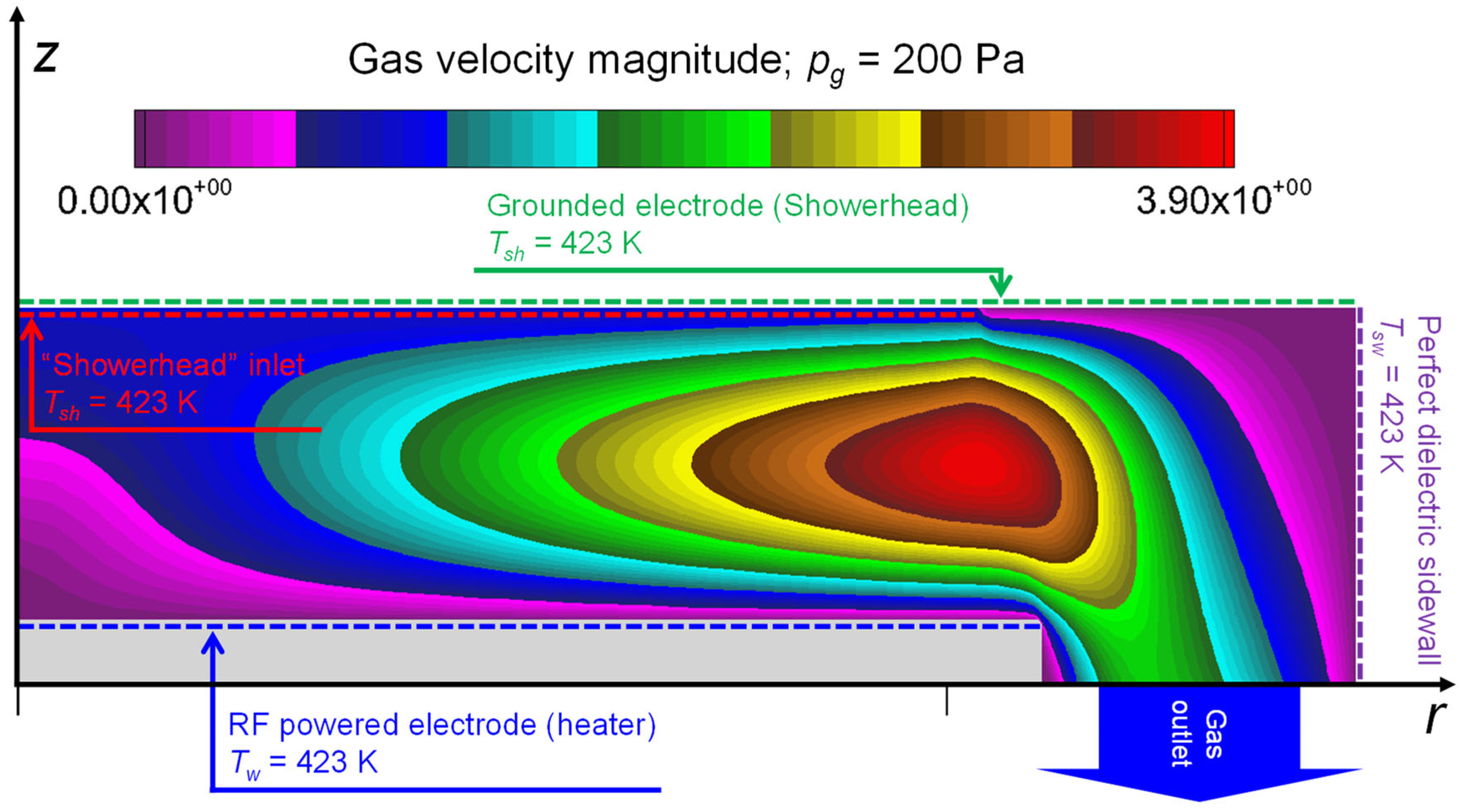
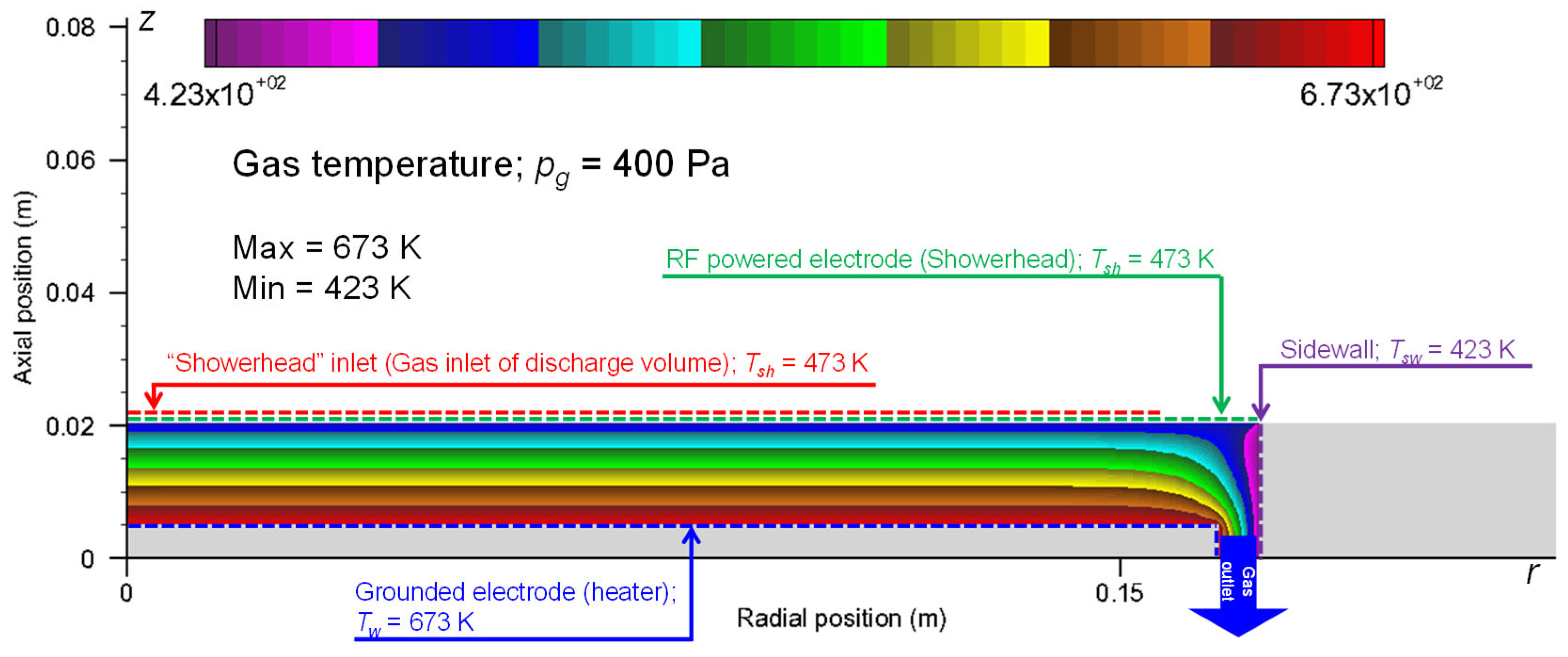
2.4. Reactor Geometry and Configuration

We now describe the geometric configuration and operating conditions for the showerhead CCP deposition reactor. Our reactor under consideration is shown schematically in Figure 1. The symmetrical nature of the reactor results in only half of it being depicted in the r-z plane, where r is the radial coordinate and z is the axial coordinate. Processing wafers normally takes place in a cylindrical reactor. A symmetrical axis is represented on the left border and a sidewall is represented on the right boundary. There is a top electrode (showerhead electrode) on our cylindrical CCP reactor, separated from the (dielectric or grounded) ring-shaped component. A ring-shaped component’s inner surface serves as the sidewall.
At 13.56 MHz, voltage is applied to the top electrode (or bottom electrode), while the bottom electrode (or top electrode) is grounded. In cases with non-isothermal boundary conditions, the bottom electrode is referred to as the heater because the wafer is sometimes heated during process optimization. A silicon (Si, lossy dielectric; dielectric constant, k ≈ 12) wafer is placed on top of the bottom electrode. In order to resolve the electrical discontinuity at the wafer edge, a Si ring (also referred to as an edge ring) is placed around the wafer. Table 1 lists the details of the sixteen cases considered in this study.

3. Results

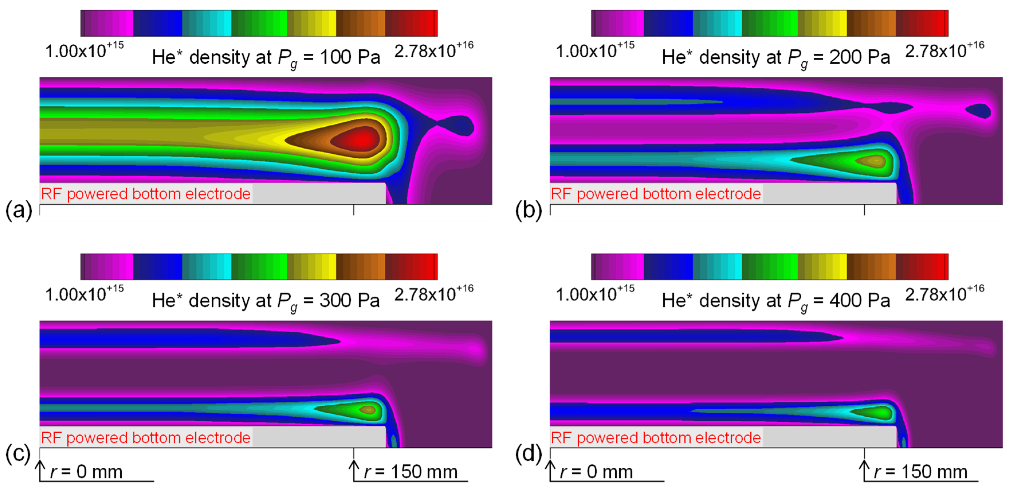
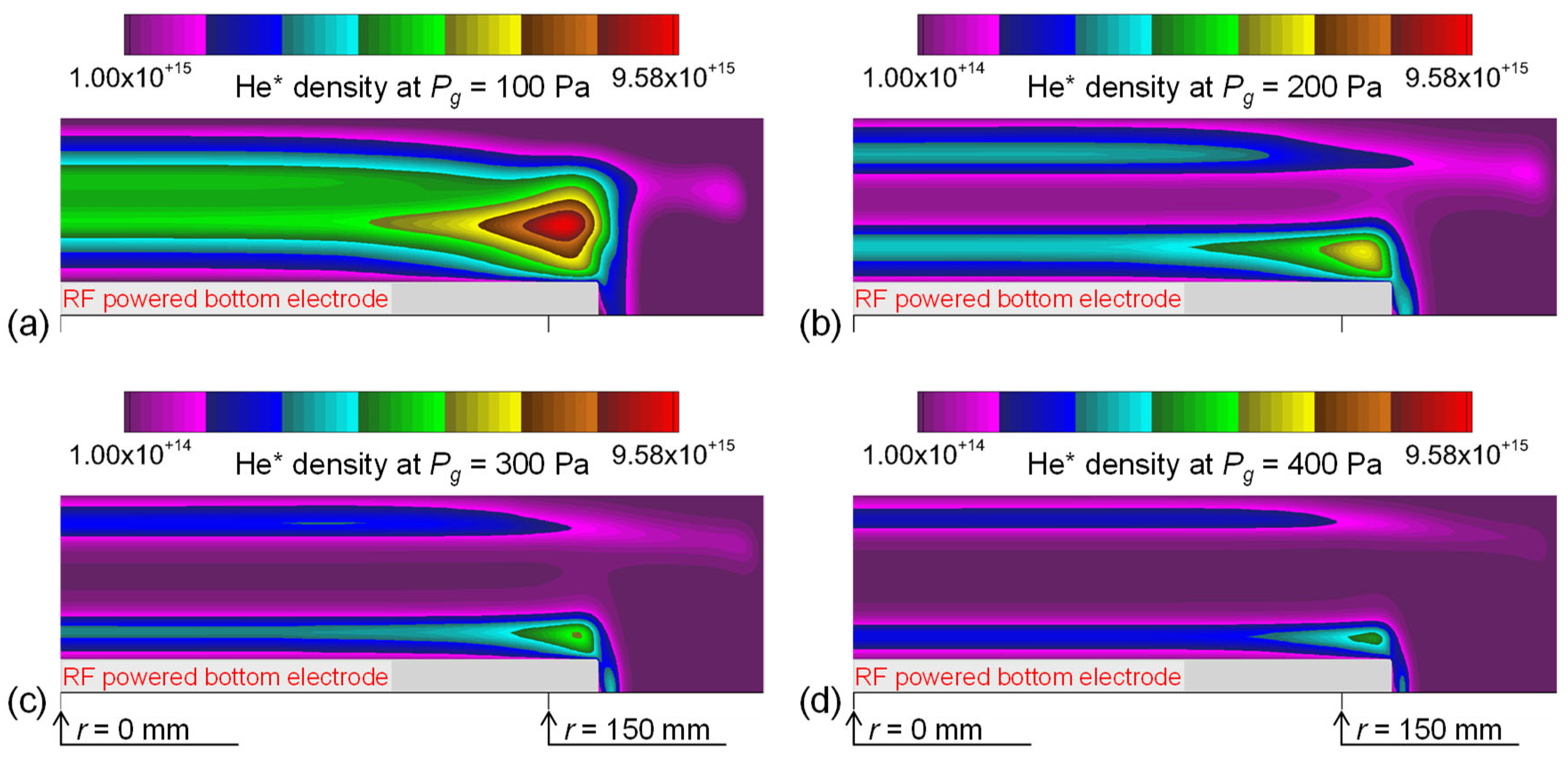
3.1. Effects of the Gas Pressure on He* Density Distributions in He-Only Discharges

Based on our previous studies, we found that plasma distribution characteristics change significantly with gas pressure. As the ion-neutral collision rate increases with higher pressure, the mean free path decreases. It increases ion and electron density and, consequently, decreases the sheath width by decreasing the drift-diffusion loss rate of charged species at the electrodes. Therefore, the focus of this section is our observation that changes in gas pressure affect the spatial variation in plasma parameters as a result of the He* density distributions.
The spatial variations in the excitation (He + e → He* + e) and ionization (He + e → He+ + e + e) rates for Case 1 (He only discharge; see Table 1), as well as the electron power density (W m−3) and electron density (Ne, m−3), respectively, are shown in Figure 2a–d. We set the gas pressure at 200 Pa, the applied RF power at 100 W, and the He flow rate at 5000 sccm.
In Figure 2a,b, excitation and ionization rates increase near the edge of the “bottom powered electrode”, with an axial shift towards it due to electrons heated by the sheath. Source functions for He* and He+ have essentially the same shape. A radial extreme in the excitation rate and ionization rate distributions is caused by electrical field enhancement at the electrode edge, which creates additional sheath heating. A shift in the extreme towards the bottom-powered electrode is also produced as a result. The electron power density in the bulk region varies only slightly, as shown in Figure 2c. Note that near corners, converging sheaths produce a large heating rate, where electron power density is maximum. The electrons diffuse from the site of production in an axial direction and the peak electron density is seen near the maximum of the ionization rate distribution, as shown in Figure 2d.
We display the He* density distributions at 200 Pa (Case 1), 400 Pa (Case 2), 800 Pa (Case 3), and 1600 Pa (Case 4) to observe the gas pressure effects thereon. It was common for input conditions to be set at 100 W of power and 5000 sccm of flow.
The distribution of He* in the axial direction between electrodes is fairly symmetrical at pg = 200 Pa. As shown in Figure 3a, He* density peaks near the electrode edges in accordance with the source function. At pg = 200 Pa, the electron density shows a similar profile. Similar profiles are not surprising since electrostatic excitation, the main source of He*, has a distribution that is essentially identical to ionization. Both profiles should be similar so long as diffusion dominates transport.
The peak density of He* shifts slightly toward the bottom-powered electrode as the gas pressure increases to 400 Pa, resulting in a noticeable skew in the profile of Figure 3b. In Figure 3c, the skew is more evident when the gas pressure is increased further to 800 Pa and the density of He* falls closer to the bottom electrode. In Figure 3d, it can be observed at 1600 Pa that the density of He* peaks at the edge of the powered electrode at the bottom and, in addition, a secondary peak can also be observed at the center of the grounded electrode at the top.
It can be identified that He* moved towards the bottom electrode and its skew towards the corner as the pressure increased, which was principally determined by the reduction in electron mean free paths and the increase in He* quenching due to the increased pressure. The electron mean free path becomes shorter as the gas pressure increases, while electron density increases as the gas pressure increases. Therefore, electrons heated by the plasma sheath and located at the powered electrode are able to dissipate their energy by excitation closer to the electrode. By increasing the electron density, the sheath thickness and velocity decrease, resulting in less energetic sheath heated electrons with a shorter dissipation length. With the collapse of the sheath (and pre-sheath), the electric field enhancement along the edge of the electrode becomes more pronounced, causing a larger skew in the He* profile. At higher pressures, the mean free path of electrons is sufficiently short for the collapsing sheath, resulting from the increase in power deposition to have an effect on the He* source function. Due to the increased plasma density, quenching of He* also increases, thus, restricting the He* nearer to the source of generation, therefore, causing it to be confined closer to its location.

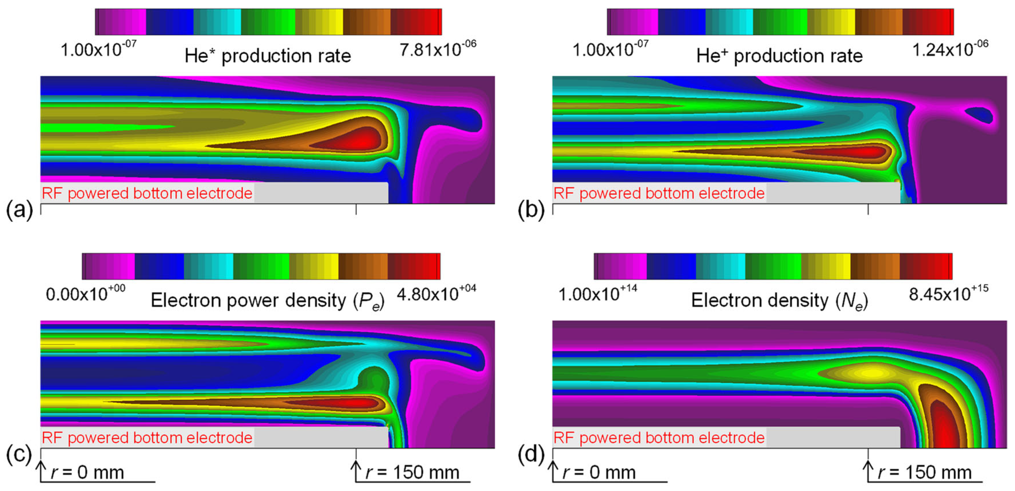
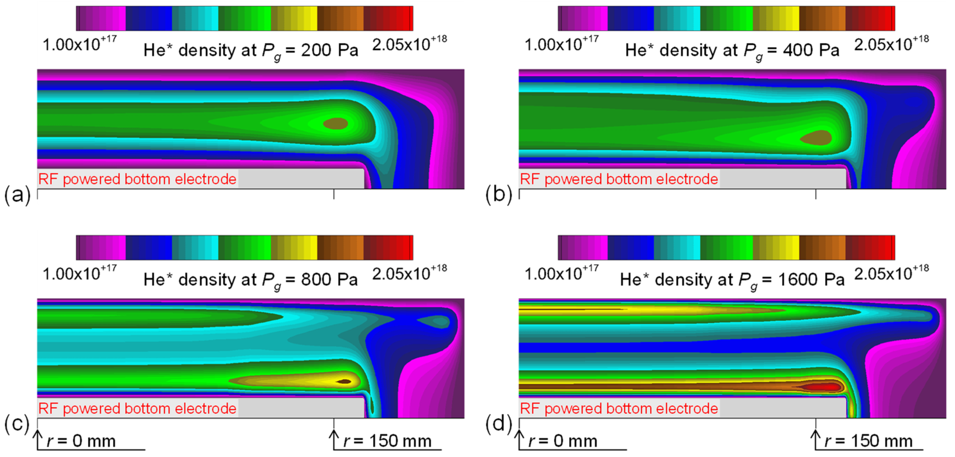
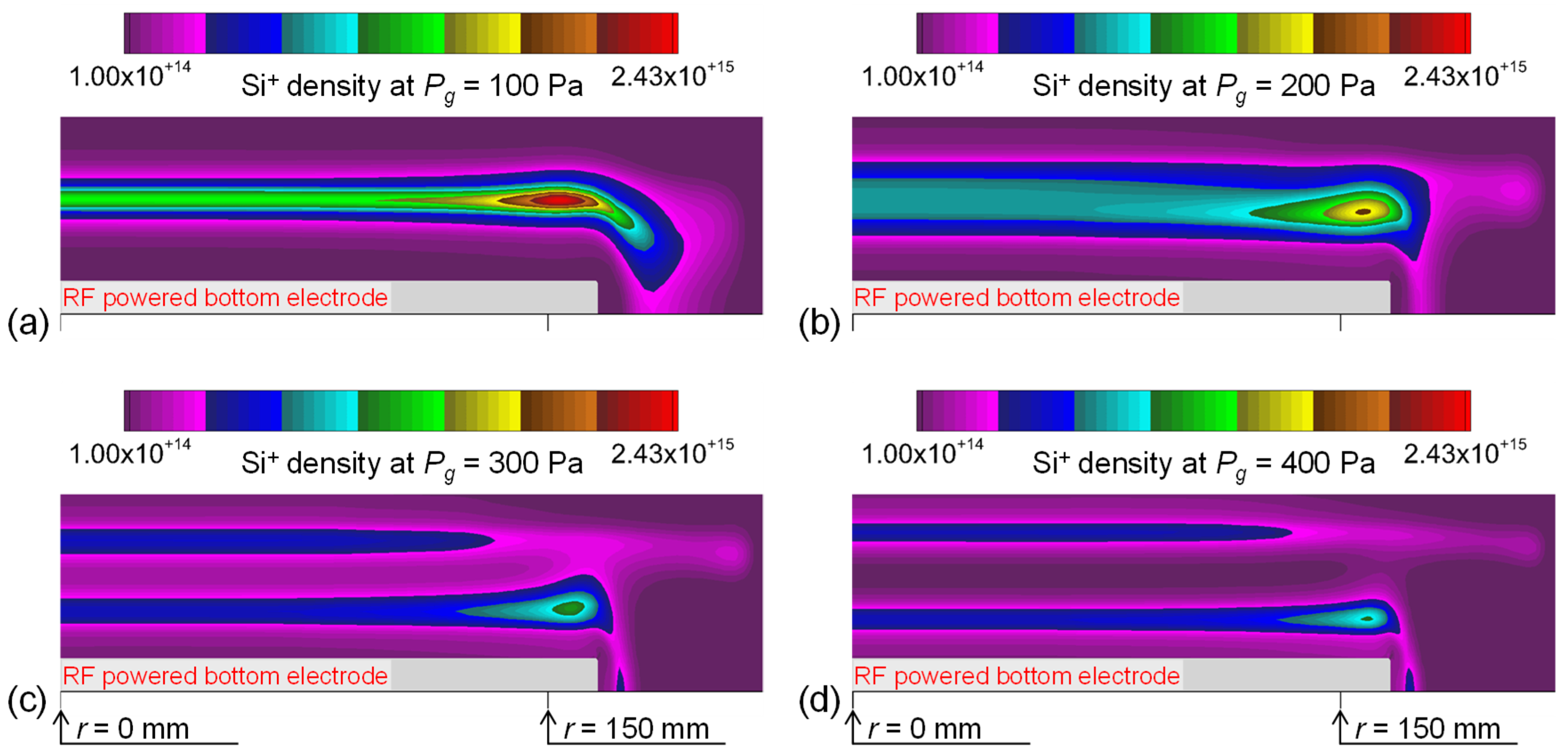
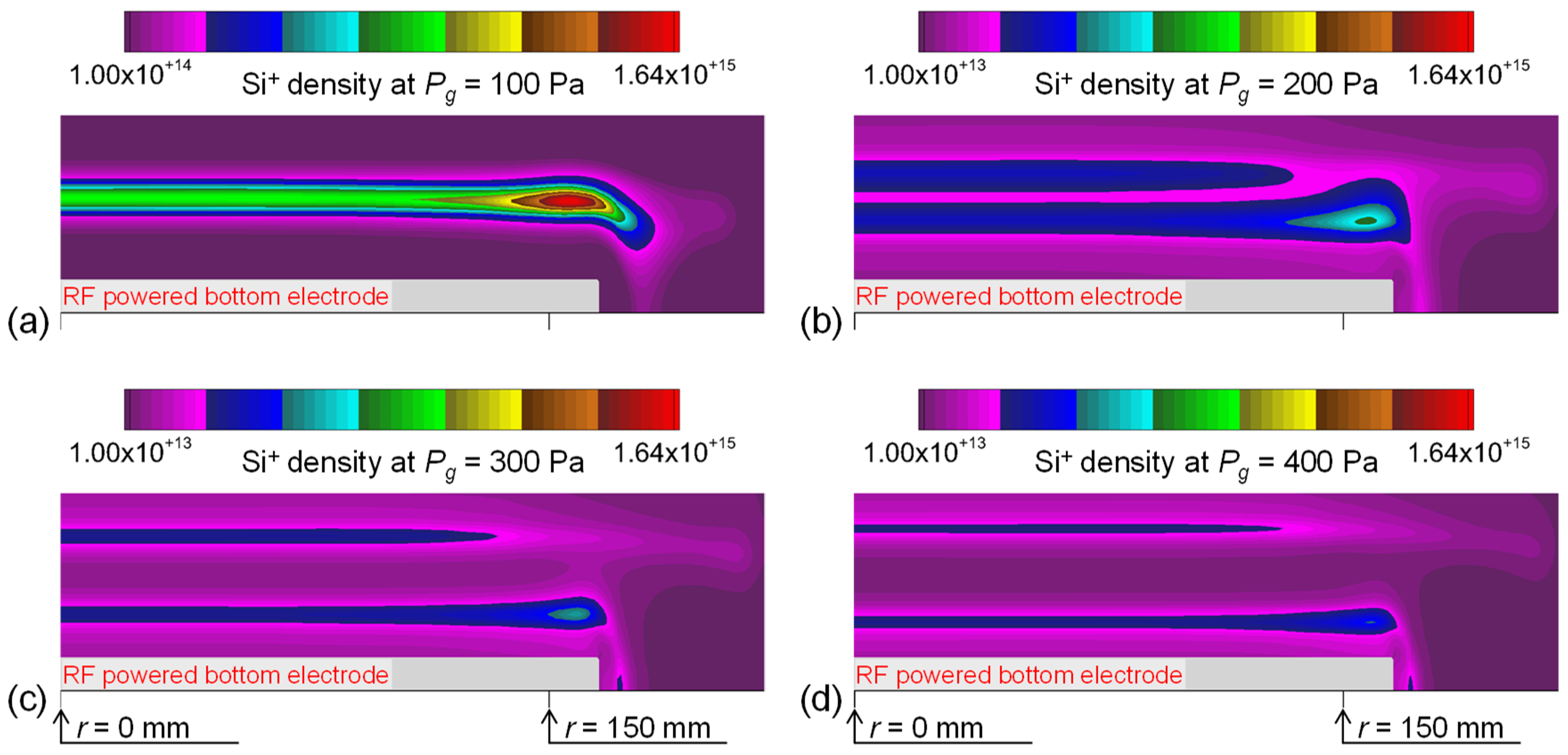
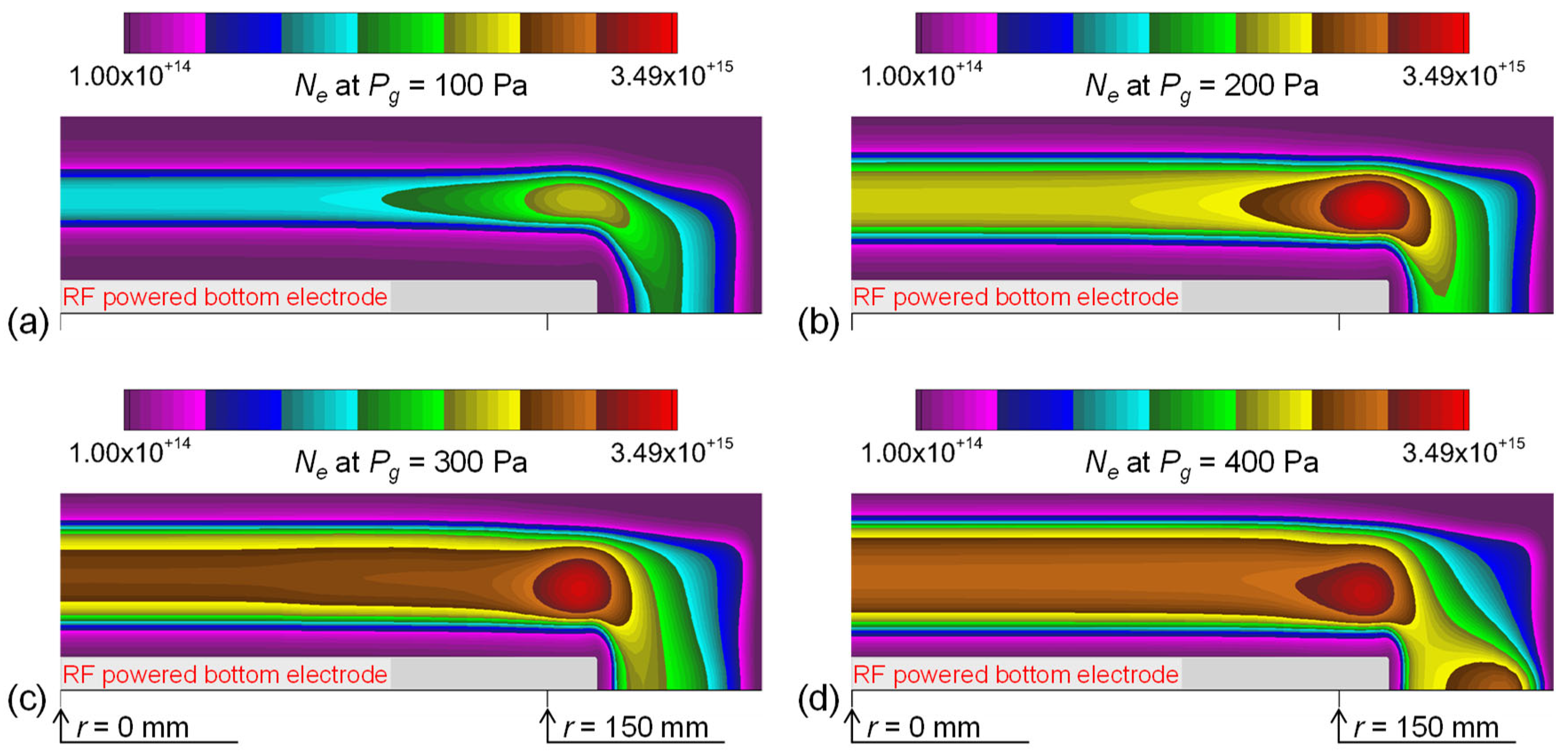
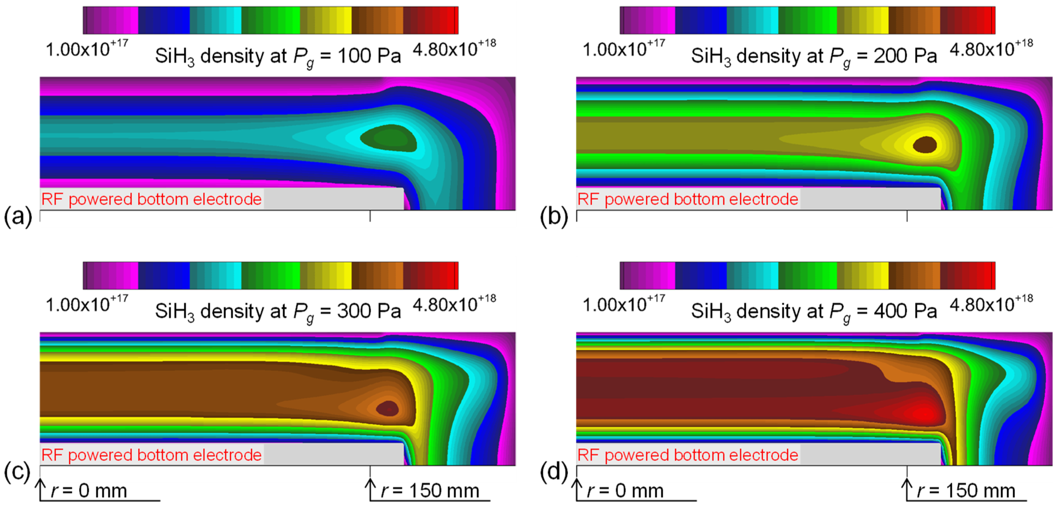
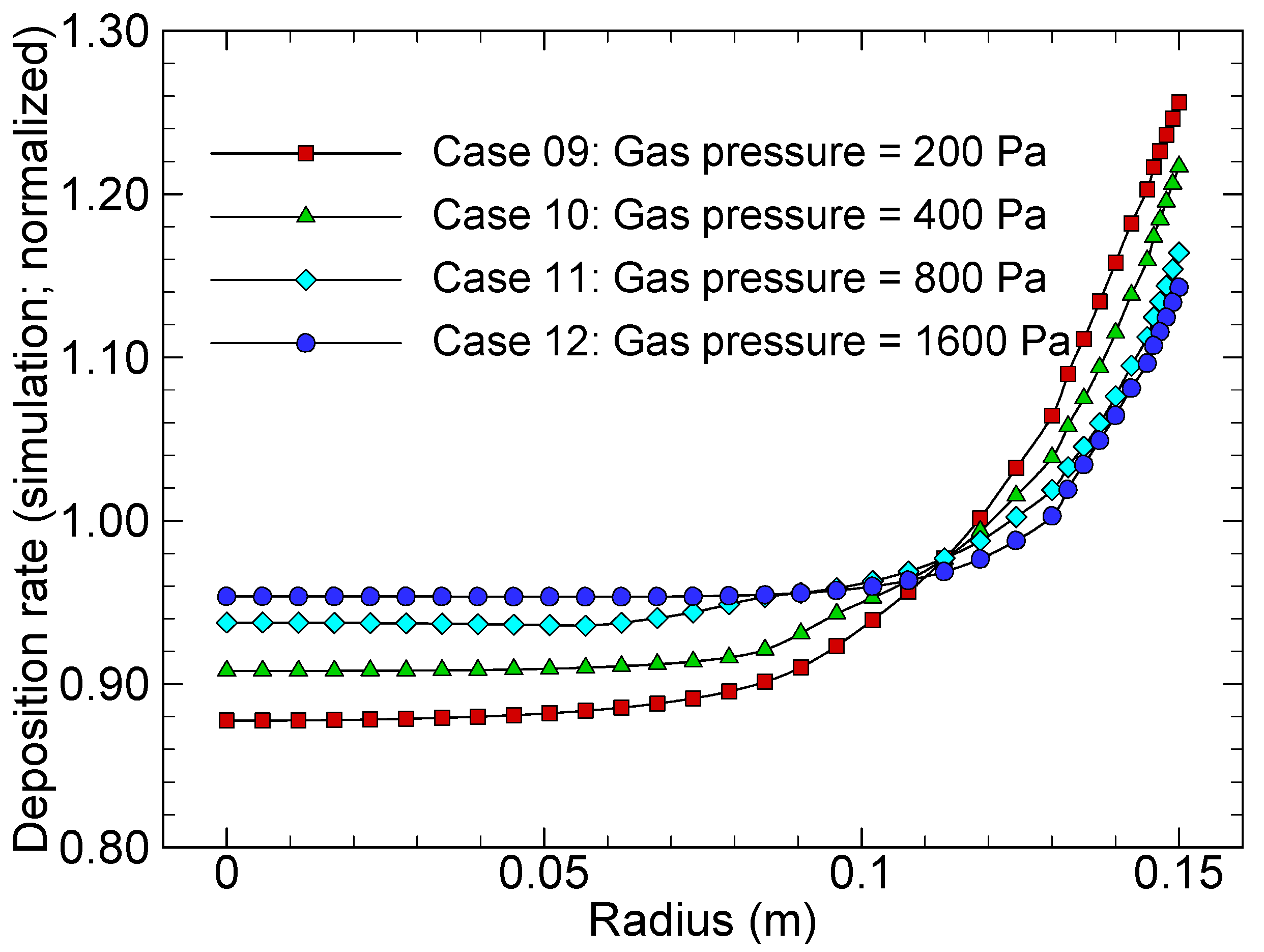
3.2. Effects of SiH4 Addition on Plasma Density Distributions in He/SiH4 Discharges

Because He* quenching has a high-reaction-rate coefficient, we numerically examined noticeable alterations to the He* density by adding SiH4 in this study. In a case at pg = 100 Pa (Cases 5), a case at pg = 200 Pa (Cases 6), a case at pg = 300 Pa (Case 7), and a case at pg = 400 Pa (Case 8), a mixture of 50 sccm SiH4 and 5000 sccm He (so the mole fraction of SiH4 is only about 1%) was used as the feed gas. As in the previous cases, the feed gas was set to be supplied from the showerhead and the applied RF power of 100 W was applied to the bottom electrode in the same manner.
The density profile of He* obtained by varying the gas pressure is shown in Figure 4 for Cases 5 (pg = 100 Pa), 6 (pg = 200 Pa), 7 (pg = 300 Pa), and 8 (pg = 400 Pa). In pure helium, because of reasons that were discussed earlier, the density profile of He* in pure helium is slightly skewed and the peak occurs near the edge of the electrode at pg ≥ 400 Pa. However, even though SiH4 is mixed with only about 1 percent, the profile shape is substantially altered, even at a lower gas pressure of pg = 200 Pa in Case 6. Furthermore, the peak density of He* decreases as a result of the quenching of He* by SiH4. A case at pg = 300 Pa (Case 7) and a case at pg = 400 Pa (Case 8) demonstrate the following: their He* density profiles show more skewness (double-humped shape in the inter-electrode region) because of the higher gas pressure.
In the same way, Figure 5 shows the time-averaged Si+ density profiles for Cases 5, 6, 7, and 8. As a result of the inlet condition (He dilution), although the threshold energy for SiH4 ionization is lower than that for He excitation or ionization, the peak value for Si+ production rate by dissociative excitation (He* quenching) is higher than that for SiH2+ production rate by direct-impact ionization. When Case 5 (pg = 100 Pa; 50 sccm SiH4) is considered, the peak value of Si+ production rate due to dissociative excitation is 8.9 × 10⁻⁷ kmol m−3 s−1, while the peak value of SiH2+ production rate due to direct-impact ionization is 7.0 × 10⁻⁷ kmol m−3 s−1. Additionally, the peak value of the Si+ density is determined by the peak value of the He* density. Kushner, subsequently, set the branching and rate coefficients for He* quenching by SiH4 as follows [30]:
He* + SiH4 → Si+ + 2H + H2 + He + e, kr = 1.3 × 10⁻¹⁶ m3 s−1.
In this equation, kr represents the reaction rate coefficient.
Expecting higher He* quenching effects, the amount of SiH4 fed in Cases 9 (He = 5000 sccm; SiH4 = 100 sccm; pg = 100 Pa), 10 (He = 5000 sccm; SiH4 = 100 sccm; pg = 100 Pa), 11 (He = 5000 sccm; SiH4 = 100 sccm; pg = 100 Pa), and 12 (He = 5000 sccm; SiH4 = 100 sccm; pg = 100 Pa) was two-times the amount fed in Cases 5, 6, 7, and 8; we increased the SiH4 flow rate to 100 sccm in Cases 9, 10, 11, and 12. Similar to Cases 5, 6, 7, and 8, we also varied the gas pressure in Cases 9 (pg = 100 Pa), 10 (pg = 200 Pa), 11 (pg = 300 Pa), and 12 (pg = 400 Pa). Figure 6 and Figure 7 show results of the time-averaged density profiles of He* and Si+ for Cases 9, 10, 11, and 12. By comparison with Cases 5, 6, 7, and 8, the He* density profile exhibits a more severe skewness caused by the heightened effect of quenching He*. Consequently, a significantly larger skewness is observed in the Si+ density profile.
The time-averaged electron density profiles for Cases 9, 10, 11, and 12 are shown in Figure 8. In most of these cases, the off-axis maxima of the electron density (Neo) are observed near the bottom electrode edge as a result of the excitation and ionization rate distributions. A similar comparison is shown in Figure 9, where time-averaged SiH3 density profiles are shown for Cases 9, 10, 11, and 12. In Cases 9, 10, 11, and 12, off-axis maxima of the SiH3 density are also observed near the bottom-electrode edge.
For a case of 2% SiH4 at pg = 100 Pa (Case 9), a case of 2% SiH4 at pg = 200 Pa (Case 10), a case of 2% SiH4 at pg = 300 Pa (Case 11), and a case of 2% SiH4 at pg = 400 Pa (Case 12), their deposition rate profiles are compared in Figure 10. The simulated deposition rate profiles are normalized using their corresponding average values. These profiles have one important characteristic in common: at 0 mm ≤ r ≤ 120 mm, they are nearly flat, but their shapes vary greatly at r > 120 mm. Recent semiconductor processing prohibits these abrupt changes.

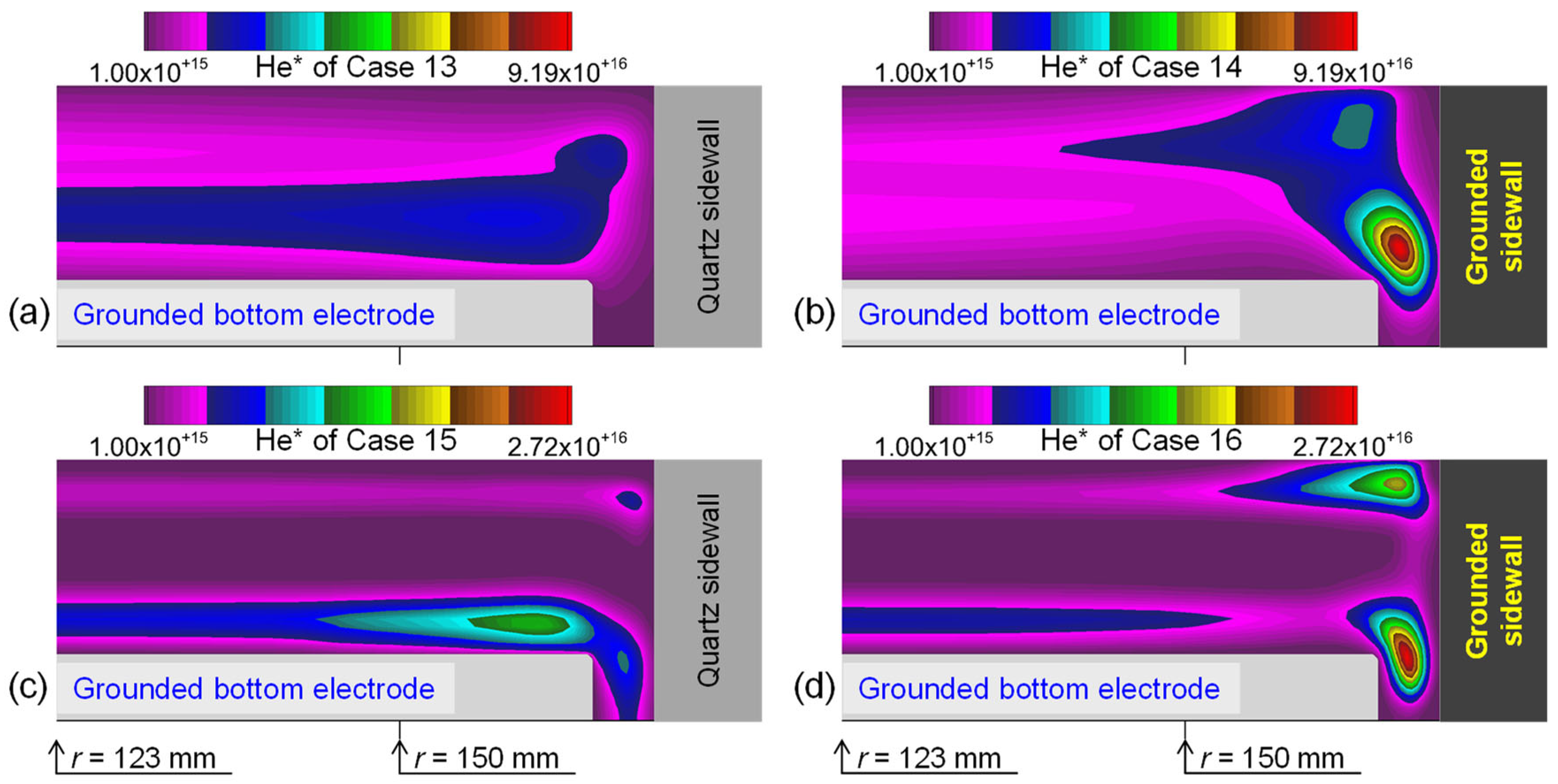
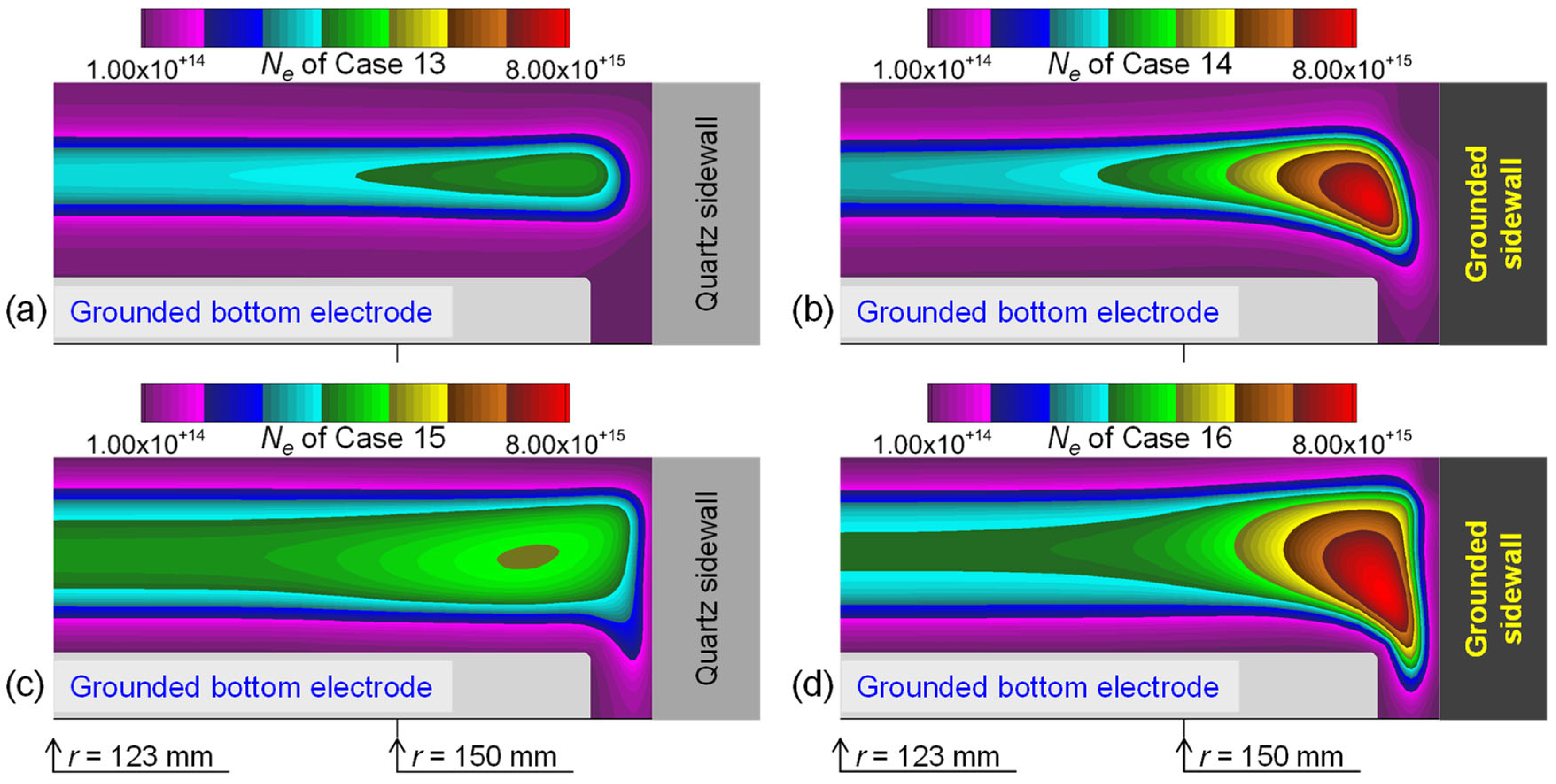
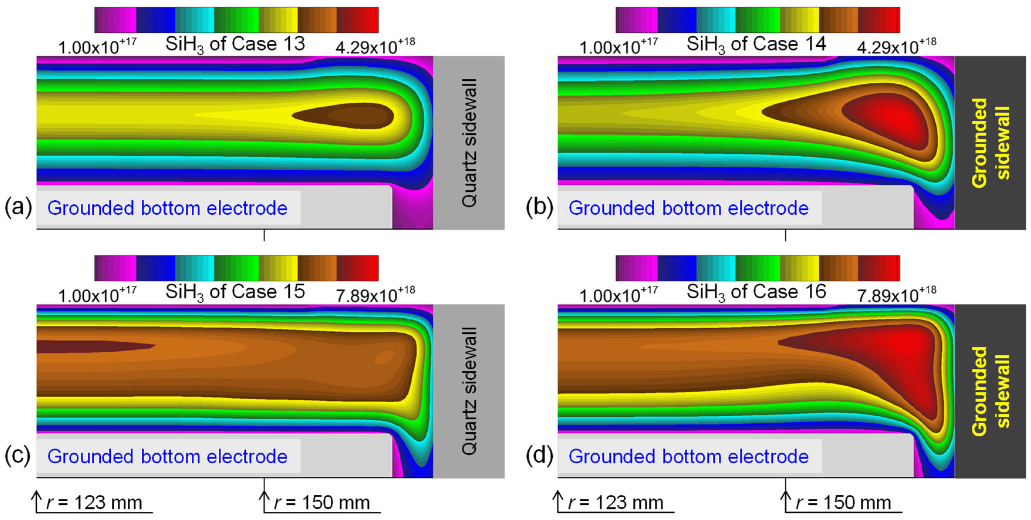
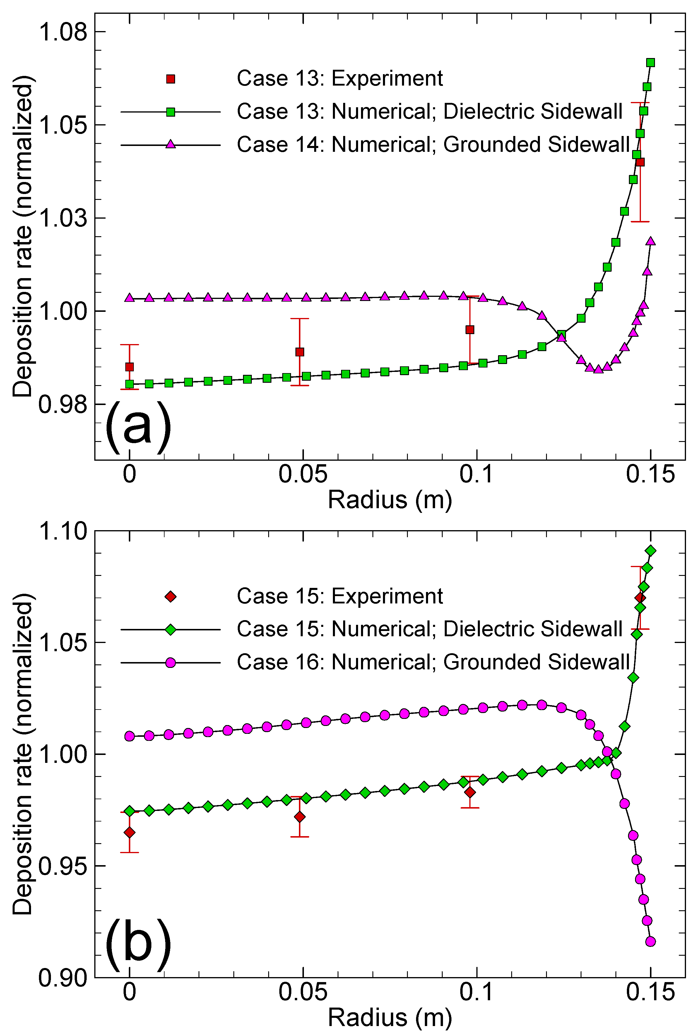
3.3. Effects of the Modified Reactor Geometry

Due to the fact that the He* and Si+ density distributions are localized near the bottom-electrode edge in the previous He/SiH4 mixture cases, the electron and SiH3 density distributions are also localized. As a result, the profiles of deposition rates for Cases 9, 10, 11, and 12 all increase abruptly in the vicinity of the edges. To resolve the localization problem, we examined the effects of the modified reactor geometry in this section (to obtain sufficient uniformity).
Figure 11 shows the modified reactor. Not only did we reduce the electrode spacing (d = 15 mm) but also the radial gap between the bottom electrode and the sidewall. In the design of industrial reactors, reducing the reactor geometry is preferable. As a mimic of our experimental apparatus, we set the top electrode to receive RF power and the bottom electrode to be grounded. The sidewall boundary condition was altered in cases with the modified reactor from dielectric to grounded. We used a quartz sidewall with a finite thickness (45 mm) for experimental validation for cases with a dielectric sidewall, instead of a perfect dielectric sidewall (See Figure 1). In order to maintain consistency, a small amount of 50 sccm SiH4 was diluted in 5000 sccm He and a frequency of 13.56 MHz VRF was applied.
Furthermore, it is noteworthy that the results presented so far pertain to isothermal wall reactors, where the showerhead surface, the sidewall surface, and the wafer surface were all maintained at the same temperature (Tsh = Tsw = Tw = 423 K; See Figure 1). In practice, however, PECVD was performed frequently under non-isothermal wall boundary conditions to control the process results. Our reactor is set up so that the showerhead temperature (Tsh) is 473 K, the sidewall temperature (Tsw) is 423 K, and the wafer temperature (Tw) is 673 K, in order to achieve non-isothermal wall boundary conditions. In Figure 11, for the modified reactor, the effect of non-isothermal wall boundary conditions on gas temperature distributions is shown (Tsh = 473 K, Tsw = 423 K, and Tw = 673 K).
Modulating the electrode temperature allows the film properties to be controlled, since the deposition is taking place on the bottom electrode. Due to the previous validation of our surface model under the Tw = 673 K condition, we decided to use the non-isothermal wall temperature condition. We chose a shorter distance between the top and bottom electrodes to achieve better process uniformity. Additionally, the shorter distance between the bottom electrode and the sidewall facilitates easier control of plasma distribution by changing the sidewall conditions. The bottom electrode was grounded since the RF-powered electrode enhances the electrode edge effect more. Furthermore, the bottom electrode in our experimental apparatus is grounded.
Figure 12 depicts the time-averaged He* density profiles obtained by varying the sidewall condition from dielectric to grounded by increasing the gas pressure from 400 to 1200 Pa for Case 13 (pg = 400 Pa; modified geometry; quartz sidewall), Case 14 (pg = 400 Pa; modified geometry; grounded sidewall), Case 15 (pg = 1200 Pa; modified geometry; quartz sidewall), and Case 16 (pg = 1200 Pa; modified geometry; grounded sidewall). Because the electric fields are enhanced near the top- and bottom-electrode edges, no matter what the gas conditions and sidewall conditions are, the excitation occurs efficiently. These four cases exhibit radially uniform excitation rate profiles at r < 130 mm. Due to strong local electric fields and the narrow gaps between the bottom electrode and the grounded sidewall, the surface losses of electrons and ions are enhanced when the grounded sidewall is present. Therefore, between the case with the dielectric sidewall at pg = 400 Pa (Cases 13) and the case with the grounded sidewall at pg = 400 Pa (Case 14) and between the case with the dielectric sidewall at pg = 1200 Pa (Cases 15) and the case with the grounded sidewall at pg = 1200 Pa (Case 16) there is a huge difference in the distributions of plasma parameters: cases with quartz sidewalls have lower peak values of He* density than cases with grounded sidewalls. In addition, for cases with grounded sidewalls, the density profiles of He* are distorted near the bottom-electrode edge, regardless of the gas pressure. In cases with the quartz sidewall, despite the fact that the peak values are located a little closer to the edge of the wafer, the He* density profiles are relatively uniform across the inter-electrode region, regardless of gas pressure.
The contours in Figure 13a–d illustrate the time-averaged electron density profiles for Cases 13, 14, 15, and 16, respectively. A similar feature can be seen in Figure 12, where radial distributions of He* density are uniform at r > 130 mm and, since the electron density profile corresponds to He* density profiles, peak electron densities are seen near the electrode edges in Figure 13. Comparing the case with the dielectric sidewall at pg = 400 Pa (Cases 13) with the case with the dielectric sidewall at pg = 1200 Pa (Cases 15) and the case with the grounded sidewall at pg = 400 Pa (Cases 14) with the case with the grounded sidewall at pg = 1200 Pa (Cases 16), although the gas pressure is higher, the electron density profiles are more uniform in the radial direction for Case 15 and Case 16, respectively. By suppressing the disturbance effect that arises not only from the shape of the electrode edge but also from the narrow electrode spacing (d = 15 mm), the distribution of electron density becomes more uniform. The suppression of the disturbance is primarily the result of electrons moving radially inwards. Additionally, the peak electron density increases in Case 14 and Case 16, regardless of the gas pressure when the sidewall condition changes from dielectric to grounded. The bulk electron densities, however, are maintained at similar levels. The thinner sheath thickness on the dielectric sidewall is detected, regardless of the gas pressure. The result is an improvement in the plasma uniformity in the inter-electrode region.
In Figure 14a–d, we illustrate the time-averaged SiH3 density profiles for Cases 13, 14, 15, and 16, respectively. Gas pressure affects the differences between the local maximum SiH3 densities (on-axis maximum values detected on the axis). In spite of the common edge-high distributions among the four cases, there are still substantial differences in the details, especially near the electrode edges: radial changes in the thickness of boundary layers are occurring. The phenomenon is explained by the fact that there are non-negligible differences between the off-axis maxima of the electron densities (Neo). Neo’s difference in position causes the radical density field to behave differently at the edge of the electrode due to a difference in boundary layer thickness. Moreover, since the grounded sidewall induces a thicker radial sheath for Cases 14 and Case 16, their radial positions of Neo and their maximum SiH3 density are detected farther away from the sidewall.
In Figure 15a, the deposition rate profiles for Cases 13 and 14 are compared and in Figure 15b, those for Cases 15 and 16 are compared. The simulated deposition rate profiles are normalized using their corresponding average values. Deposition rate profiles for Cases 13 and 15 match well with experimental data for their respective cases. This comparison was performed in the radial direction due to the axisymmetry in the experimental data. Azimuthal non-uniformity is indicated by the error bars. It is apparent that all profiles have an important feature in common: when 0 mm ≤ r ≤ 130 mm, their shapes are nearly flat; at r > 130 mm, however, their shapes vary greatly. By using the grounded sidewall, the areas of the effective grounded surfaces are enlarged, which results in a reduction in the surface fluxes of charged species near the bottom-electrode edge. It is mostly the result of distortion of the electric potential distribution caused by the higher gas pressure. Thus, in Cases 14 and 16, the thicker bottom sheath induced at approximately r = 150 mm reduces the deposition rate profile, whereas the dielectric sidewall significantly increases the deposition rate in Cases 13 and 15.

4. Conclusions

In this study, we numerically investigated helium metastable distributions and their effects on the uniformity of hydrogenated amorphous silicon depositions in He/SiH4 CCPs. We presented the results of a two-dimensional fluid model of He discharges and then the results of He/SiH4 discharges to deposit hydrogenated amorphous silicon films. Utilizing a 300 mm wafer reactor in the semiconductor industry, we investigated what factor determines the uniformity of plasma density distribution.
As observed in Cases 5–12, excitation and ionization rate profiles were enhanced and localized near the electrode edge when a reactor similar to GECRC was used. We, therefore, investigated the effects of modifying the reactor geometry in order to improve uniformity in Cases 13–16. In the modification, we reduced the electrode spacing and the radial gap between the bottom electrode and the sidewall. In addition, by toggling the sidewall condition from dielectric to grounded and by varying the gas pressure (from 400 Pa to 1200 Pa), we observed that the effect of the sidewall on the deposition rate profiles was affected by the gas pressure. Regardless of the gas pressure, for the dielectric sidewall, the thinner sheath thickness on the sidewall was detected and the plasma uniformity was improved in the inter-electrode region.

Author Contributions

Conceptualization, H.J.K.; Data curation, S.K. and H.J.K.; Formal analysis, S.J., S.K., K.L. and H.J.K.; Funding acquisition, K.L. and H.J.K.; Investigation, S.K., K.L. and H.J.K.; Methodology, S.J., S.K. and H.J.K.; Project administration, H.J.K.; Resources, H.J.K.; Software, H.J.K.; Supervision, H.J.K.; Validation, S.J. and H.J.K.; Visualization, S.J. and H.J.K.; Writing—original draft, S.J. and H.J.K.; Writing—review and editing, K.L. and H.J.K. All authors have read and agreed to the published version of the manuscript.

Funding

This work was supported by the Gachon University research fund of 2020 (GCU-202008470001). This work was supported by Korea Institute for Advancement of Technology (KIAT) grant funded by Korea Government (MOTIE) (P0020612, 2022 The Competency Development Program for Industry Specialist).

Institutional Review Board Statement

Not applicable.

Informed Consent Statement

Not applicable.

Data Availability Statement

Data sharing is not applicable to this article.

Conflicts of Interest

The authors declare no conflict of interest.

References

  1. Marr, B. The 5 Biggest Data Science Trends in 2022. Available online: https://www.forbes.com/sites/bernardmarr/2021/10/04/the-5-biggest-data-science-trends-in-2022/?sh=1afe2df40d3f (accessed on 27 February 2022).
  2. Kim, M.; Park, E.; Kim, I.S.; Park, J.; Kim, J.; Jeong, Y.; Lee, S.; Kim, I.; Park, J.-K.; Seong, T.-Y.; et al. A Comparison Study on Multilayered Barrier Oxide Structure in Charge Trap Flash for Synaptic Operation. Crystals 2021, 11, 70. [Google Scholar] [CrossRef]
  3. Smith, D.L. Thin-Film Deposition: Principles and Practice; McGraw-Hill: New York, NY, USA, 1995. [Google Scholar]
  4. Lieberman, M.A.; Lichtenberg, A.J. Principles of Plasma Discharges and Materials Processing; John Wiley & Sons, Inc.: Hoboken, NJ, USA, 2005. [Google Scholar]
  5. Knoops, H.C.M.; Faraz, T.; Arts, K.; Kessels, W.M.M.E. Status and prospects of plasma-assisted atomic layer deposition. J. Vac. Sci. Technol. A 2019, 37, 030902. [Google Scholar] [CrossRef]
  6. Kim, H.J. Effect of electrode heating on the distribution of the ion production rate in a capacitively coupled plasma deposition reactor in consideration of thermal decomposition. Vacuum 2021, 189, 110264. [Google Scholar] [CrossRef]
  7. Kim, H.J. Influence of the gas pressure in a Torr regime capacitively coupled plasma deposition reactor. Plasma Sources Sci. Technol. 2021, 30, 065001. [Google Scholar] [CrossRef]
  8. Yavas, O.; Richter, E.; Kluthe, C.; Sickmoeller, M. Wafer-edge yield engineering in leading-edge DRAM manufacturing. Semicond. Fabtech 2009, 39, 1–5. [Google Scholar]
  9. Hwang, S.; Kanarik, K. Available online: https://sst.semiconductor-digest.com/2016/08/evolution-of-across-wafer-uniformity-control-in-plasma-etch/ (accessed on 27 February 2022).
  10. Maydan, D. The future of equipment development and semiconductor production. Mater. Sci. Eng. A 2001, 302, 1–5. [Google Scholar] [CrossRef]
  11. Zhang, B.; Zhang, X. Control of higher-silane generation by dilution gases in SiH4 plasmas. Plasma Sources Sci. Technol. 2020, 29, 095012. [Google Scholar] [CrossRef]
  12. McMillin, B.K.; Zachariah, M.R. Two-dimensional argon metastable density measurements in a radio frequency plasma reactor by planar laser-induced fluorescence imaging. J. Appl. Phys. 1995, 77, 5538–5544. [Google Scholar] [CrossRef]
  13. McMillin, B.K.; Zachariah, M.R. Two-dimensional laser-induced fluorescence imaging of metastable density in low-pressure radio frequency argon plasmas with added O2, Cl2, and CF4. J. Appl. Phys. 1996, 79, 77–85. [Google Scholar] [CrossRef]
  14. Sharma, S.; Sirse, N.; Turner, M.M.; Ellingboe, A.R. Influence of excitation frequency on the metastable atoms and electron energy distribution function in a capacitively coupled argon discharge. Phys. Plasmas 2018, 25, 063501. [Google Scholar] [CrossRef]
  15. Kovalev, A.S.; Rakhimova, T.V.; Rakhimov, A.T.; Proshina, O.V.; Vasilieva, A.N.; Voloshin, D.G. Dynamics of Ar metastable and resonance states in pulsed capacitively coupled plasmas. Phys. Plasmas 2021, 28, 093507. [Google Scholar] [CrossRef]
  16. Wen, D.-Q.; Krek, J.; Gudmundsson, J.T.; Kawamura, E.; Lieberman, M.A.; Verboncoeur, J.P. Particle-in-Cell Simulations with Fluid Metastable Atoms in Capacitive Argon Discharges: Electron Elastic Scattering and Plasma Density Profile Transition. IEEE Trans. Plasma Sci. 2022, 30, 105009. [Google Scholar] [CrossRef]
  17. Babaeva, N.Y.; Kushner, M.J. Penetration of plasma into the wafer-focus ring gap in capacitively coupled plasmas. J. Appl. Phys. 2007, 101, 113307. [Google Scholar] [CrossRef]
  18. Yang, Y.; Kushner, M.J. Graded conductivity electrodes as a means to improve plasma uniformity in dual frequency capacitively coupled plasma sources. J. Phys. D Appl. Phys. 2010, 43, 152001. [Google Scholar] [CrossRef]
  19. Bi, Z.-H.; Dai, Z.-L.; Zhang, Y.-R.; Liu, D.-P.; Wang, Y.-N. Effects of reactor geometry and frequency coupling on dual-frequency capacitively coupled plasmas. Plasma Sources Sci. Technol. 2013, 22, 055007. [Google Scholar] [CrossRef]
  20. Kim, H.J.; Lee, H.J. Uniformity control of the deposition rate profile of a-Si:H film by gas velocity and temperature distributions in a capacitively coupled plasma reactor. J. Appl. Phys. 2018, 123, 113302. [Google Scholar] [CrossRef]
  21. Kim, H.J.; Lee, H.J. Numerical analysis of the effect of electrode spacing on deposition rate profiles in a capacitively coupled plasma reactor. Plasma Sources Sci. Technol. 2016, 25, 065006. [Google Scholar] [CrossRef]
  22. Kim, H.J.; Yang, W.; Joo, J. Effect of electrode spacing on the density distributions of electrons, ions, and metastable and radical molecules in SiH4/NH3/N2/He capacitively coupled plasmas. J. Appl. Phys. 2015, 118, 043304. [Google Scholar] [CrossRef]
  23. Kim, H.J.; Lee, H.J. 2D fluid model analysis for the effect of 3D gas flow on a capacitively coupled plasma deposition reactor. Plasma Sources Sci. Technol. 2016, 25, 035006. [Google Scholar] [CrossRef]
  24. Kim, H.J.; Lee, H.J. Analysis of intermediate pressure SiH4/He capacitively coupled plasma for deposition of an amorphous hydrogenated silicon film in consideration of thermal diffusion effects. Plasma Sources Sci. Technol. 2017, 26, 085003. [Google Scholar] [CrossRef]
  25. ESI Group. CFD-ACE+ 2020.0 Manual; ESI US R&D Inc.: Huntsville, AL, USA, 2020. [Google Scholar]
  26. Kolobov, V.; Arslanbekov, R. Deterministic Boltzmann solver for electron kinetics in plasma reactors for microelectronics applications. Microelectron. Eng. 2003, 69, 606–615. [Google Scholar] [CrossRef]
  27. Farouk, T.; Farouk, B.; Staack, D.; Gutsol, A.; Fridman, A. Simulation of dc atmospheric pressure argon micro glow-discharge. Plasma Sources Sci. Technol. 2006, 15, 676–688. [Google Scholar] [CrossRef]
  28. Farouk, T.; Farouk, B.; Gutsol, A.; Fridman, A. Atmospheric pressure methane-hydrogen dc micro-glow discharge for thin film deposition. J. Phys. D Appl. Phys. 2008, 41, 175202. [Google Scholar] [CrossRef]
  29. Mouchtouris, S.; Kokkoris, G. A novel plasma fluid model for fast 2D calculations in capacitively coupled atmospheric pressure plasma jets. Plasma Sources Sci. Technol. 2021, 30, 01LT01. [Google Scholar] [CrossRef]
  30. Kushner, M.J. Simulation of the gas-phase processes in remote-plasma-activated chemical-vapor deposition of silicon dielectrics using rare gas-silane-ammonia mixtures. J. Appl. Phys. 1992, 9, 4173–4189. [Google Scholar] [CrossRef] [Green Version]
Figure 1. Schematic diagram of our CCP reactor. Spatial variation in the gas velocity magnitude (Vm, m s−1) is depicted for Case 1.
Coatings 12 01342 g001
Figure 2. Contour plots for the spatial profiles of the time-averaged (a) He* production rate for Case 1 and (b) He+ production rate for Case 1 for r ≥ 0 mm. Contour plots for the spatial profiles of the time-averaged (c) electron power density (W m−3) for Case 1 and (d) electron density (m−3) for Case 1 for r ≥ 0 mm.
Coatings 12 01342 g002
Figure 3. The spatial profiles of the time-averaged He* density (m−3) (a) for Case 1, (b) for Case 2, (c) for Case 3, and (d) for Case 4.
Coatings 12 01342 g003
Figure 4. The spatial profiles of the time-averaged He* density (m−3) (a) for Case 5, (b) for Case 6, (c) for Case 7, and (d) for Case 8.
Coatings 12 01342 g004
Figure 5. The spatial profiles of the time-averaged Si+ density (m−3) (a) for Case 5, (b) for Case 6, (c) for Case 7, and (d) for Case 8.
Coatings 12 01342 g005
Figure 6. The spatial profiles of the time-averaged He* density (m−3) (a) for Case 9, (b) for Case 10, (c) for Case 11, and (d) for Case 12.
Coatings 12 01342 g006
Figure 7. The spatial profiles of the time-averaged Si+ density (m−3) (a) for Case 9, (b) for Case 10, (c) for Case 11, and (d) for Case 12.
Coatings 12 01342 g007
Figure 8. The spatial profiles of the time-averaged electron density (Ne, m−3) (a) for Case 9, (b) for Case 10, (c) for Case 11, and (d) for Case 12.
Coatings 12 01342 g008
Figure 9. The spatial profiles of the time-averaged SiH3 density (m−3) (a) for Case 9, (b) for Case 10, (c) for Case 11, and (d) for Case 12.
Coatings 12 01342 g009
Figure 10. Deposition rate profiles are plotted for Cases 9, 10, 11, and 12. The profiles are normalized with their corresponding averaged values.
Coatings 12 01342 g010
Figure 11. Schematic diagram of the modified CCP reactor. Spatial variation in the gas temperature (Tg, K) is depicted for Case 13.
Coatings 12 01342 g011
Figure 12. The spatial profiles of the time-averaged He* density (m−3) (a) for Case 13 (b) for Case 14, (c) for Case 15, and (d) for Case 16.
Coatings 12 01342 g012
Figure 13. The spatial profiles of the time-averaged electron density (Ne, m−3) (a) for Case 13, (b) for Case 14, (c) for Case 15, and (d) for Case 16.
Coatings 12 01342 g013
Figure 14. The spatial profiles of the time-averaged SiH3 density (m−3) (a) for Case 13, (b) for Case 14, (c) for Case 15, and (d) for Case 16.
Coatings 12 01342 g014
Figure 15. Effect of the sidewall and the gas pressure on the deposition rates. (a) The deposition rate profiles of Cases 13 and 14 are compared. Experimental data from Case 13 are superimposed on the profile of Case 13. (b) The deposition rate profiles of Cases 15 and 16 are compared. Experimental data from Case 15 are superimposed on the profile of Case 15. The profiles are normalized with their corresponding averaged values.
Coatings 12 01342 g015
Table 1. List of cases considered in this study.
Case No.He
Flow Rate
SiH4
Flow Rate
Sidewall
Condition
Gas
Pressure
Electrode
Spacing
Sidewall
Gap
15000 sccm-Perfect Dielectric200 Pa25 mm52 mm
25000 sccm-Perfect Dielectric400 Pa25 mm52 mm
35000 sccm-Perfect Dielectric800 Pa25 mm52 mm
45000 sccm-Perfect Dielectric1600 Pa25 mm52 mm
55000 sccm50 sccmPerfect Dielectric100 Pa25 mm52 mm
65000 sccm50 sccmPerfect Dielectric200 Pa25 mm52 mm
75000 sccm50 sccmPerfect Dielectric300 Pa25 mm52 mm
85000 sccm50 sccmPerfect Dielectric400 Pa25 mm52 mm
95000 sccm100 sccmPerfect Dielectric100 Pa25 mm52 mm
105000 sccm100 sccmPerfect Dielectric200 Pa25 mm52 mm
115000 sccm100 sccmPerfect Dielectric300 Pa25 mm52 mm
125000 sccm100 sccmPerfect Dielectric400 Pa25 mm52 mm
135000 sccm50 sccmQuartz400 Pa15 mm7 mm
145000 sccm50 sccmGrounded400 Pa15 mm7 mm
155000 sccm50 sccmQuartz1200 Pa15 mm7 mm
165000 sccm50 sccmGrounded1200 Pa15 mm7 mm
Publisher’s Note: MDPI stays neutral with regard to jurisdictional claims in published maps and institutional affiliations.

