Article

A Study on the Characteristics of Inductively Coupled Plasma Nitridation Process

1
Plasma E.I. Convergence Research Center, Korea Institute of Fusion Energy, Gunsan-si 54004, Korea
2
Fundamental Technology Research Division, Institute of Plasma Technology, Korea Institute of Fusion Energy, Gunsan-si 54004, Korea
*
Author to whom correspondence should be addressed.
Coatings 2022, 12(10), 1372; https://doi.org/10.3390/coatings12101372
Submission received: 8 July 2022 / Revised: 14 September 2022 / Accepted: 16 September 2022 / Published: 20 September 2022
(This article belongs to the Special Issue New Advances in Plasma Deposition and Its Applications)

Abstract

:
In this study, we investigated the nitridation of silicon oxide film surfaces using an inductively coupled plasma source. The plasma parameters and nitride film characteristics were measured under various nitrogen gas pressures and radio frequency power levels. Plasma parameters such as electron density, electron temperature, and ion density were measured and analyzed using several instruments. The nitridation characteristics of the thin films were characterized using X-ray photoelectron spectroscopy. The findings provide information on the correlation between nitridation rate and process parameters.

1. Introduction

Plasma nitriding is a useful technique for altering the surface properties of materials. For example, complementary metal oxide semiconductor (CMOS) technology uses thermally grown silicon oxide (SiO2) as a gate dielectric material because of its high reliability, high resistivity, excellent dielectric strength, low interface defect density, and large bandgap [1,2]. However, several fundamental limitations of the CMOS technology have been documented. The SiO2 thickness decreases continuously owing to the high dielectric constant required for nanoscale devices and can easily approach the thinning limit of 1 nm. The ultrathin SiO2 layer causes the following problems: the tunneling currents increase exponentially as the SiO2 thickness decreases further than 3 mm; moreover, when p+ poly-silicon is used as a gate contact in metal–oxide–semiconductor field-effect transistors (MOSFET), boron penetration into the gate dielectric material increases, which causes a threshold voltage shift in the device [1]. Silicon oxynitride (SiON) is a promising substitute for SiO2 as a gate dielectric for CMOS applications [3]. Nitridation of SiO2 dielectrics has several advantages: for example, the further reduction in the gate–equivalent oxide thickness (EOT) by increasing the dielectric constant of the material (k). The dielectric constant of oxynitrides depends on the N content. The dielectric constant increases from 3.9 (k value of SiO2) to a maximum of 7.5 (k value of Si3N4) on the introduction of N into the surface [1]. It is possible to increase the thickness of the gate material without loss of the EOT owing to the increase in the dielectric constant [4]. Therefore, it is possible to reduce the gate leakage current compared with the SiO2 dielectric. Finally, in SiON thin films, nitrogen forms a barrier that prevents dopants, especially boron atoms, from diffusing from the highly doped polysilicon gate into the dielectric [1]. This diffusion has a detrimental effect on the reliability of dielectric materials. Therefore, nitrogen incorporation increased the thermal stability of the gate dielectric [5]. Moreover, the diffusion of atomic hydrogen is reduced in SiON compared to standard SiO2 [1].
Plasma treatment technology has been used as a surface modification tool for various materials. In general, the physical and chemical properties of plasma can be determined using various parameters. Understanding the physical and chemical properties of the plasma is key to controlling the plasma process. Therefore, to improve process safety and performance, a thorough understanding of plasma characteristics is necessary [6,7,8].
The Si/SiO2 interface is located at the core of the MOSFET gate structure. The gate leakage current can be reduced appropriately by introducing sufficient nitrogen in a given oxide thickness. Plasma nitridation technology is currently under development, and studies related to nitride film formation mechanisms have been published [9].
Analytical assessments in this field are experimental, and dielectric thin films are measured using X-ray photoelectron spectroscopy (XPS). In this study, we investigated the SiON film generation mechanism based on the process parameters observed during the plasma nitridation process with a 10 nm thin oxide film.

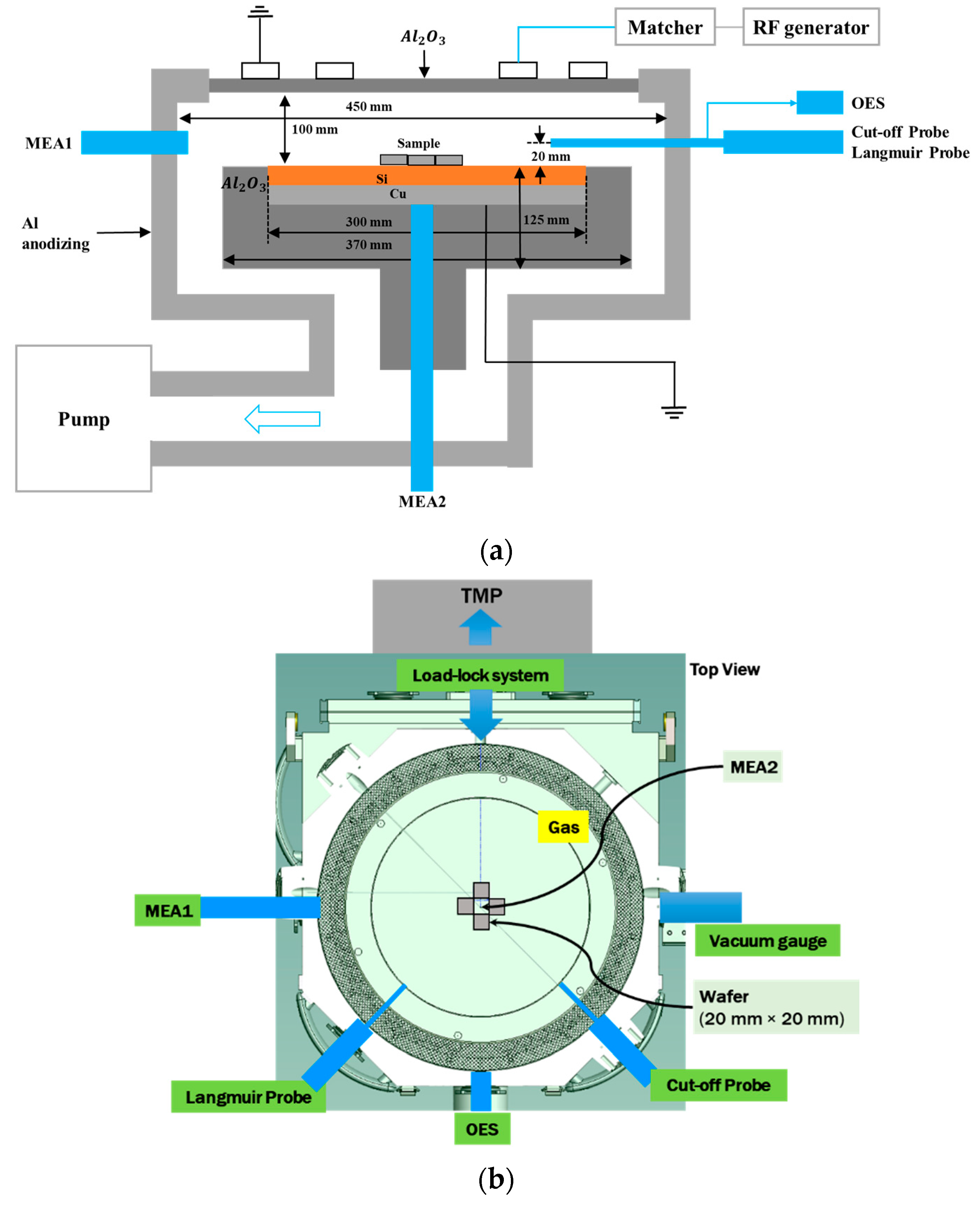
2. Materials and Methods
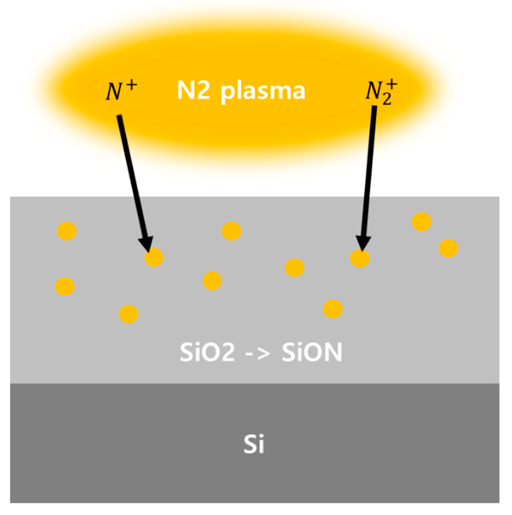
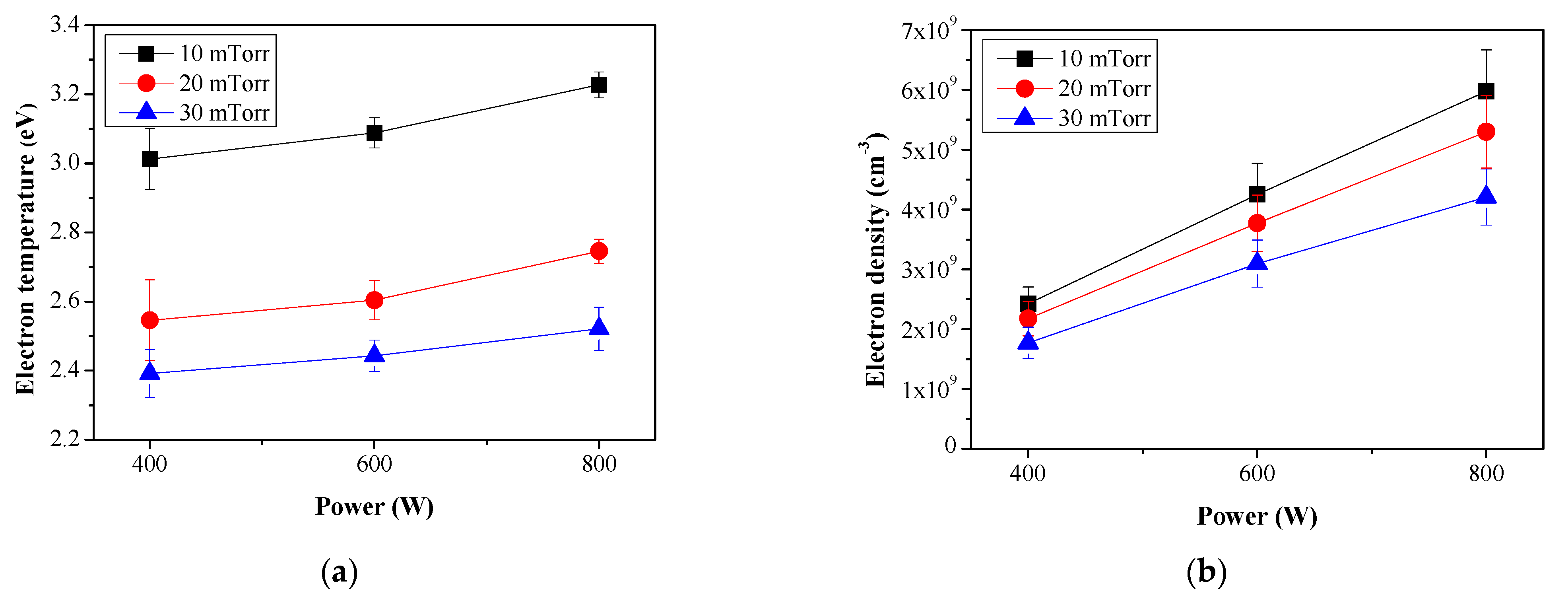
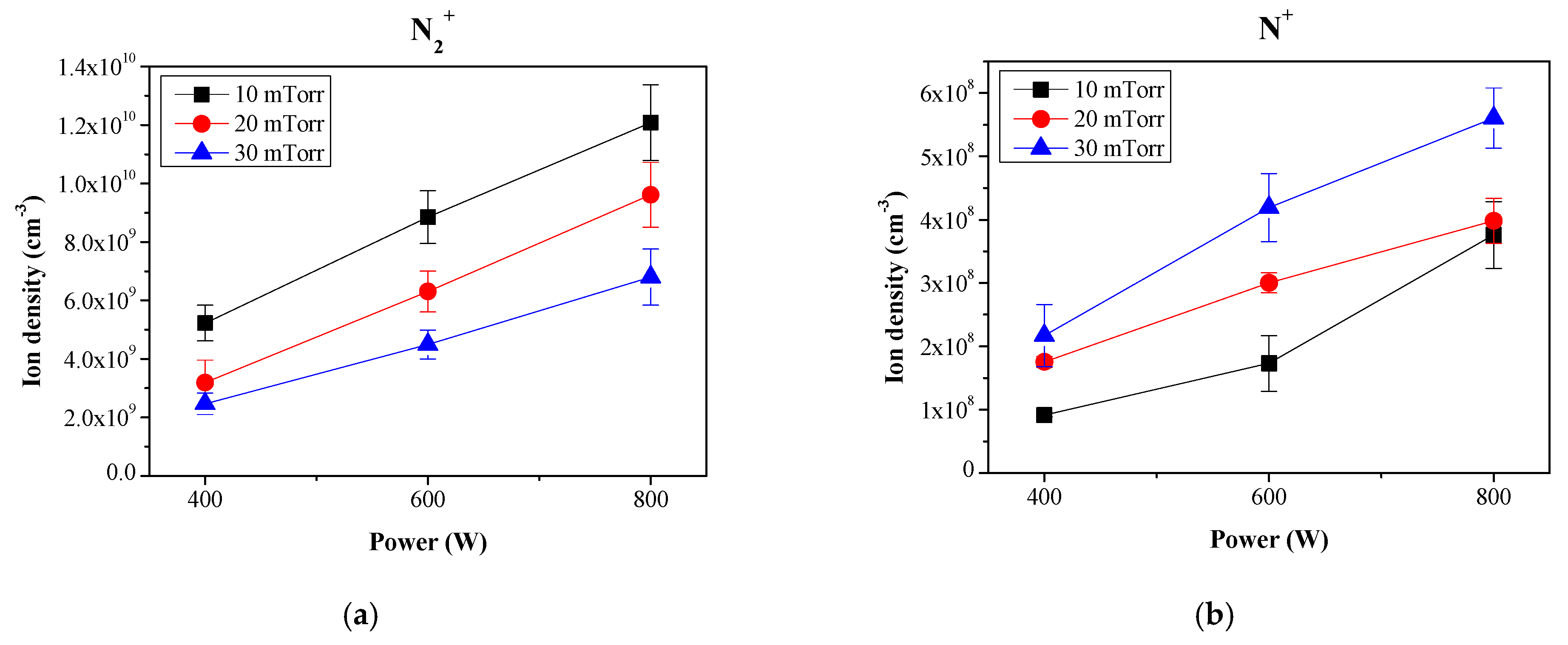
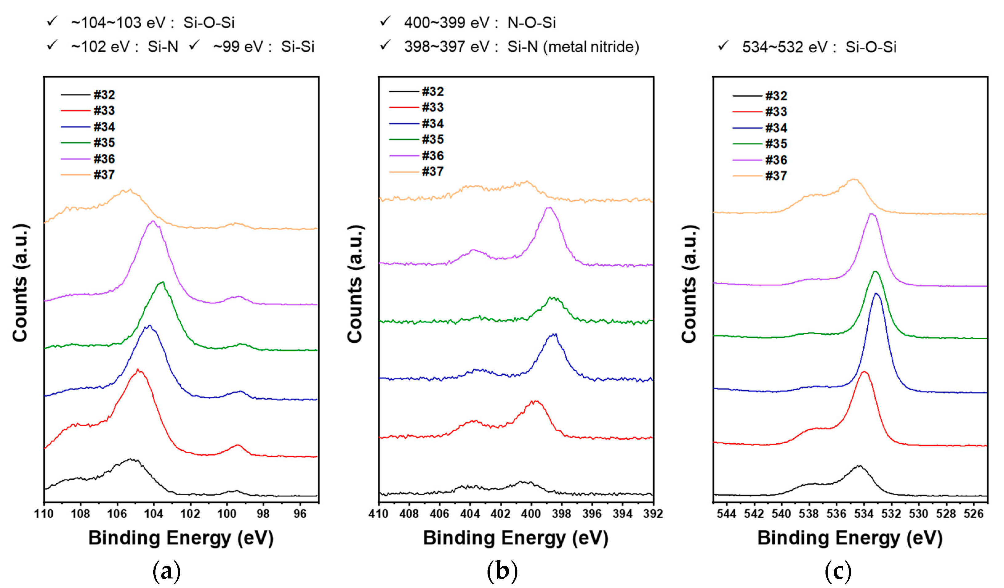
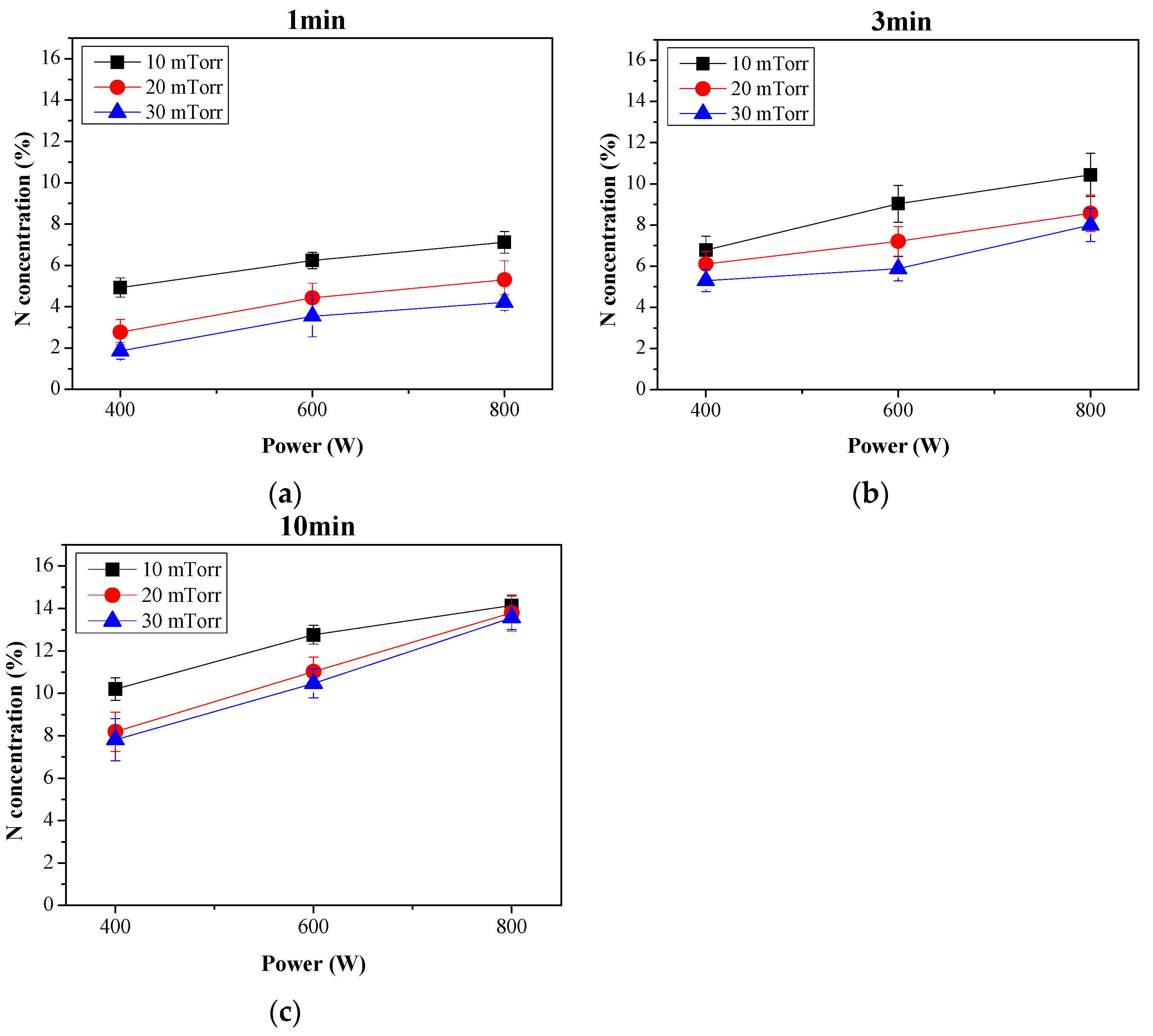
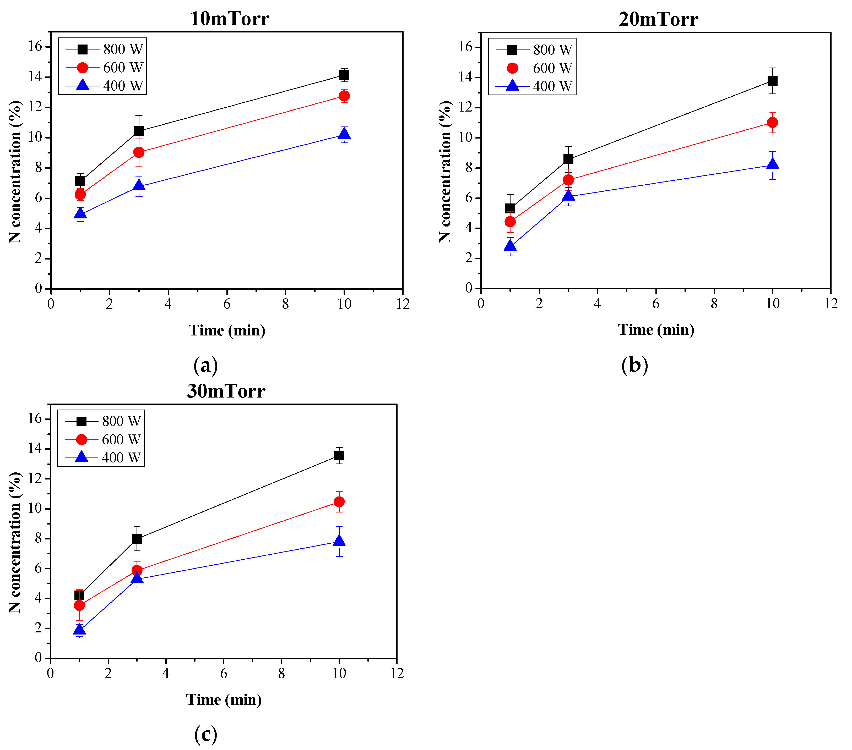
An inductively coupled plasma (ICP) system (PNICP, homemade) was used to determine the plasma properties during plasma nitriding. The process reactor used for nitriding the SiO2 film was 450 mm in diameter and had an impedance-adjustable antenna. Radio-frequency (RF) inductively coupled plasma was generated using an ICP coil antenna with a variable impedance element, powered by a 13.56 MHz RF generator (Cito Plus, Comet, Wünnewil-Flamatt, Switzerland) via an impedance-matching network (AGS, Comet, Wünnewil-Flamatt, Switzerland). The inner and outer ICP coil antennas had diameters of 160 mm and 320 mm, respectively. The ICP coil antenna was air-cooled using multiple fans for temperature stability, and the surface of the antenna was coated with silver to prevent oxidation. The ICP coil antenna was mounted on the top of the reactor using ceramic insulation. The distance between the ceramic insulator and the substrate was 100 mm, and the substrate diameter was 300 mm. A ceramic cover was installed on the substrate to prevent direct contact with the plasma, even when the silicon wafer was not placed on the substrate. In addition, a 500 µm diameter pinhole was installed at the center of the substrate such that particles passing through the pinhole could be measured using a mass/energy analyzer. Cito Plus (13.56 MHz, 1 kW) and AGS (13.56 MHz, 1 kW) from Comet (Wünnewil-Flamatt, Switzerland) were used for the radio frequency power supply and impedance matching network, respectively. The process gas was N2 (99.999% purity) and the flow rate and pressure were controlled using a mass flow controller (MFC, Mass-Flo®, 1000sccm, MKS, Andover, MA, USA). The reactor base pressure was 10−6 Torr, which was maintained using a turbomolecular pump (STP-1303C, Edwards, Burgess Hill, UK) and dry pump (GX100N, Edwards, Burgess Hill, UK) [10]. The cut-off probe (CP) and Langmuir probe (LP) were measured 200 mm from the center of the chamber and 20 mm from the wafer surface. Two mass/energy analyzers were installed at the bottom of the substrate and on the reactor wall to measure the mass and energy of the ionic species (MEA1: PSM; MEA2: EQP, Hiden, Warrington, UK).
The measured plasma parameters include the electron temperature ( T e ), electron density ( N e ). N concentration ( N % ) of the silicon nitride oxide film is measured by XPS (K-Alpha, Thermo Scientific, Waltham, MA, USA).
In this study, a wafer on which a 10 nm SiO2 thin film formed was cut into a 20 mm × 20 mm square (Figure 1b), and the experiment was performed by loading it onto the Si substrate inside the chamber in four directions. Plasma parameters were measured at source RF power levels of 400, 600, and 800 W; process pressures of 10, 20, and 30 mTorr; and process durations of 1, 3, and 10 min. Figure 2 shows a schematic of the SiON film formation mechanism.

3. Results

One mechanism for incorporating N from the plasma into the gate oxide is to break Si−O bonds using reactive nitrogen species. Ideally, a large N concentration should be applied at the gate electrode/gate dielectric interface to efficiently block B penetration, reduce gate leakage current, and minimize channel mobility degradation. The electron energy distribution in plasma is described by the electron temperature ( T e ), which is proportional to the mean ion kinetic energy ( E i ) [11].
We developed a Langmuir probe (LP) measurement program using the LabView software. LP was used in a data acquisition circuit for measuring plasma characteristics. LP measurement cycles were approximately 1.5 s long. Voltage vs. current signal graphs measured by the probe were recorded as individual files for each measurement. The developed LP program displayed the plasma electron density ( n e ), electron temperature ( T e ), plasma potential ( V p ), floating potential ( V f ), electron saturation current ( I e s a t ), and ion saturation current ( I isat ) at the same time as the measurement.
Figure 3a shows the electron temperature dependence on the source power and pressure. Figure 3b plots the electron density dependence on the source power. It was observed that the electron temperature and electron density increased with increasing source power and decreased with increasing pressure.
Figure 4 shows the densities of the ionic species, namely, N 2 + and N + , measured through the pinholes of MEA1 (wall) and MEA2 (substrate). The channel electron multiplier (CEM) used as the detector of the MEA changes intensity depending on the operating environment and usage time. Therefore, the method of measuring the density of ions based on the area ratio of the ion energy distribution is used. The ion energy distributions (IEDs) of the four ionic species ( N 2 + , N + , H 2 O + , and O 2 + ) were measured under various experimental conditions to obtain their relative ratios. The density values of each ionic species were calculated based on the ion saturation current and electron temperature values measured by the LP. The measured relative ratios of H 2 O + and O 2 + ions were lower than 0.02% and 0.1%, respectively, and were not included in the analysis results [7].
The nitrogen ion ( N 2 + and N + ) density increases as the source power increases; accordingly, more energy is transferred to the plasma electrons, and the ionization rate increases, which in turn increases the nitrogen ion density. N + density tended to be much lower than N 2 + density because N + ions are generated by the dissociative ionization of N 2 as well as the dissociative excitation of N 2 + . As shown in Figure 4, the N + ion density increases with increasing pressure and power. However, the N 2 + density increases as the power increases but decreases as the pressure increases. N 2 + ions are the primary species in the nitrogen plasma that contribute to the nitridation of SiO2 thin films. Table 1 presents the conditions of the measurements. Figure 5 shows the XPS profiles of the samples.
Figure 6 plots the nitrogen concentration in the SiON film as a function of the process time and RF power conditions. Similar to the N 2 + density, the nitrogen concentration increases as the source power increases and pressure decreases. In the 1 min process, the nitrogen concentration increases linearly with the source power; however, the linear behavior is not exhibited as the process time increases. Figure 6c shows that the N concentration tends to approach the same value with differences within 5% at 20 mTorr and 30 mTorr in the 10 min process. At 800 W, the nitrogen concentrations reach the same value (13.56% at 30 mTorr, 13.79% at 20 mTorr, 14.14% at 10 mTorr) at all pressures, which seem to converge to a constant nitrogen concentration eventually. The nitrogen concentration in the film can be increased by enhancing the plasma source power or increasing the nitridation time. However, once the surface starts saturating with nitrogen, further nitrogen adsorption is inhibited and the nitridation rate tapers off.
Figure 7 plots the nitrogen concentrations in the thin film as a function of process time and pressure. The nitrogen concentration was expected to increase as the source power and process time increased; however, it eventually converged to a constant value. The nitrogen concentration convergence on the source power increase exhibited different characteristics depending on the pressure. This is consistent with the results obtained by Shahid Rauf [12], which indicated that the surface nitrogen concentration increased linearly with time and tended to saturate after a certain period. In Rauf’s study [12], a 1.3 nm thick SiO2 thin film showed a tendency to become saturated after 30 s. However, in this study, a 10 nm thick SiO2 thin film showed a tendency to become saturated after 10 min.

4. Conclusions

In this study, we experimentally examined the plasma nitridation mechanism of SiO2 thin films using ICP. The N 2 + ion density was observed to decrease with an increase in the process gas pressure; however, N + ions exhibited the opposite trend. On increasing the source RF power, the densities of both ions increased. Results showed that N 2 + ions, rather than N + ions, were predominantly involved in the nitridation of SiO2 thin films. The nitrogen concentration increased by increasing the source power or the nitridation time. However, the nitridation rate was observed to decrease with increasing power as the surface became saturated with nitrogen, which further reduced nitrogen incorporation in the dielectric film. The nitrogen concentration converged to approximately 14% for all pressures at the source power of 800 W. We expect that further examination of the correlation between the non-invasive measurements and plasma parameters will lead to the development of an intelligent process equipment technology that predicts nitridation rate through plasma parameters and diagnoses the plasma process equipment in real time.

Author Contributions

Conceptualization, J.-H.S., J.-B.P., Y.-H.K. and J.-S.K.; experimental work, J.-H.S., Y.-H.K., J.-B.P., D.-C.K., Y.-W.K. and J.-S.Y.; writing—original draft preparation, J.-H.S., Y.-H.K., J.-B.P. and J.-S.K.; writing—review and editing, J.-H.S. and J.-S.K. All authors have read and agreed to the published version of the manuscript.

Funding

This work was supported by the R&D program of “Plasma Equipment Intelligence Convergence Research Center (code No. 1711121944)” through the National Research Council of Science & Technology (NST) grant provided by the Korean government (MSIT) funded by the Government funds and R&D Program of “Plasma BigData ICT Convergence Technology Research Project (code No. 1711124799)” through the Korea Institute of Fusion Energy (KFE) funded by Government funds of Republic of Korea.

Institutional Review Board Statement

Not applicable.

Informed Consent Statement

Not applicable.

Data Availability Statement

Data sharing is not applicable to this article.

Conflicts of Interest

The authors declare no conflict of interest.

References

  1. Green, M.L.; Gusev, E.P.; Degraeve, R.; Garfunkel, E.L. Ultrathin (<4 nm) SiO2 and Si-O-N gate dielectric layers for silicon microelectronics: Understanding the processing, structure, and physical and electrical limits. J. Appl. Phys. 2001, 90, 2057. [Google Scholar]
  2. Wilk, G.D.; Wallace, R.M.; AnthonGreen, J.M. High-κ gate dielectrics: Current status and materials properties considerations. J. Appl. Phys. 2001, 89, 5243. [Google Scholar] [CrossRef]
  3. Szekeres, A.; Nikolova, T.; Simeonov, S.; Gushterov, A.; Hamelmann, F.; Heinzmann, U. Plasma-assisted chemical vapor deposited silicon oxynitride as an alternative material for gate dielectric in MOS devices. Microelectron. J. 2006, 37, 64–70. [Google Scholar] [CrossRef]
  4. Maheta, V.D.; Olsen, C.; Ahmed, K.; Mahapatra, S. The Impact of Nitrogen Engineering in Silicon Oxynitride Gate Dielectric on Negative-Bias Temperature Instability of p-MOSFETs: A Study by Ultrafast On-The-Fly IDLIN Technique. IEEE Trans. Electron Dev. 2008, 55, 1630–1638. [Google Scholar] [CrossRef]
  5. Hourdakis, E.; Nassiopoulou, A.G.; Parisini, A.; Reading, M.A.; van den Berg, J.A.; Sygellou, L.; Ladas, S.; Petrik, P.; Nutsch, A.; Wolf, M.; et al. Electrical and structural properties of ultrathin SiON films on Si prepared by plasma nitridation. J. Vac. Sci. Technol. B. 2011, 29, 022201. [Google Scholar] [CrossRef]
  6. Profijt, H.B.; Potts, S.E.; van de Sanden, M.C.M.; Kessels, W.M.M. Plasma-Assisted Atomic Layer Deposition: Basic, Opportunities, and Challenges. J. Vac. Sci. Technol. A 2011, 29, 050801. [Google Scholar] [CrossRef]
  7. Kanarik, K.J.; Lill, T.; Hudson, E.A.; Sriraman, S.; Tan, S.; Marks, J.M.; Vahedi, V.; Gottscho, R.A. Overview of Atomic Layer Etching in the Semiconductor Industry. J. Vac. Sci. Technol. A 2015, 33, 020802. [Google Scholar] [CrossRef]
  8. Lieberman, M.A.; Lichtenberg, A.J. Principles of Plasma Discharges and Materials Processing; Wiley-Interscience: Hoboken, NJ, USA, 2005; pp. 387–534. [Google Scholar]
  9. Lim, S.W.; Luo, T.Y.; Jiang, J. Mechanism of Silicon Dioxide Decoupled Plasma Nitridation. Jpn. J. Appl. Phys. 2006, 45, L413–L415. [Google Scholar] [CrossRef]
  10. Kim, Y.H.; Cho, J.H.; Kim, J.S.; Park, J.B.; Kim, D.C.; Kim, Y.W. Comprehensive Data Collection Device for Plasma Equipment Inelligence Studies. Coatings 2021, 11, 1025. [Google Scholar] [CrossRef]
  11. Cubaynes, F.N. Ultra-Thin Plasma Nitrided Oxide Gate Dielectrics for Advanced MOS Transistors. Ph.D. Thesis, University of Twente, Enschede, The Nederlands, 24 June 2004. [Google Scholar]
  12. Rauf, S.; Lim, S.W.; Ventzek, P.L.G. Model for nitridation of nanoscale SiO2 thin films in pulsed inductively coupled N2 plasma. J. Appl. Phys. 2005, 98, 024305. [Google Scholar] [CrossRef]
Figure 1. Schematic of the experimental device: Cut-off probe, Langmuir probe, MEA1, and MEA2. (a) side view, (b) top view.
Coatings 12 01372 g001
Figure 2. Schematic of the mechanism of creating SiON film.
Coatings 12 01372 g002
Figure 3. (a) Electron temperature dependence on power, (b) electron density dependence on power.
Coatings 12 01372 g003
Figure 4. Ion density dependence on power: (a) N 2 + and (b) N + ion density.
Coatings 12 01372 g004
Figure 5. XPS spectra of the (a) Si 2p, (b) N 1s, (c) O 1s region of XPS spectra.
Coatings 12 01372 g005
Figure 6. N concentration in the SiON film at (a) 1 min, (b) 3 min, and (c) 10 min.
Coatings 12 01372 g006
Figure 7. N concentration in the SiON film at (a) 10 mTorr, (b) 20 mTorr, and (c) 30 mTorr.
Coatings 12 01372 g007
Table 1. Experimental conditions for XPS measurements. (#: Experimental number).
10 min
400 W600 W
10 mTorr20 mTorr30 mTorr10 mTorr20 mTorr30 mTorr
#32#33#34#35#36#37
Publisher’s Note: MDPI stays neutral with regard to jurisdictional claims in published maps and institutional affiliations.

