
Comparative Study on the Separate Extraction of Interface and Bulk Trap Densities in Indium Gallium Zinc Oxide Thin-Film Transistors Using Capacitance–Voltage and Current–Voltage Characteristics

Abstract
:1. Introduction
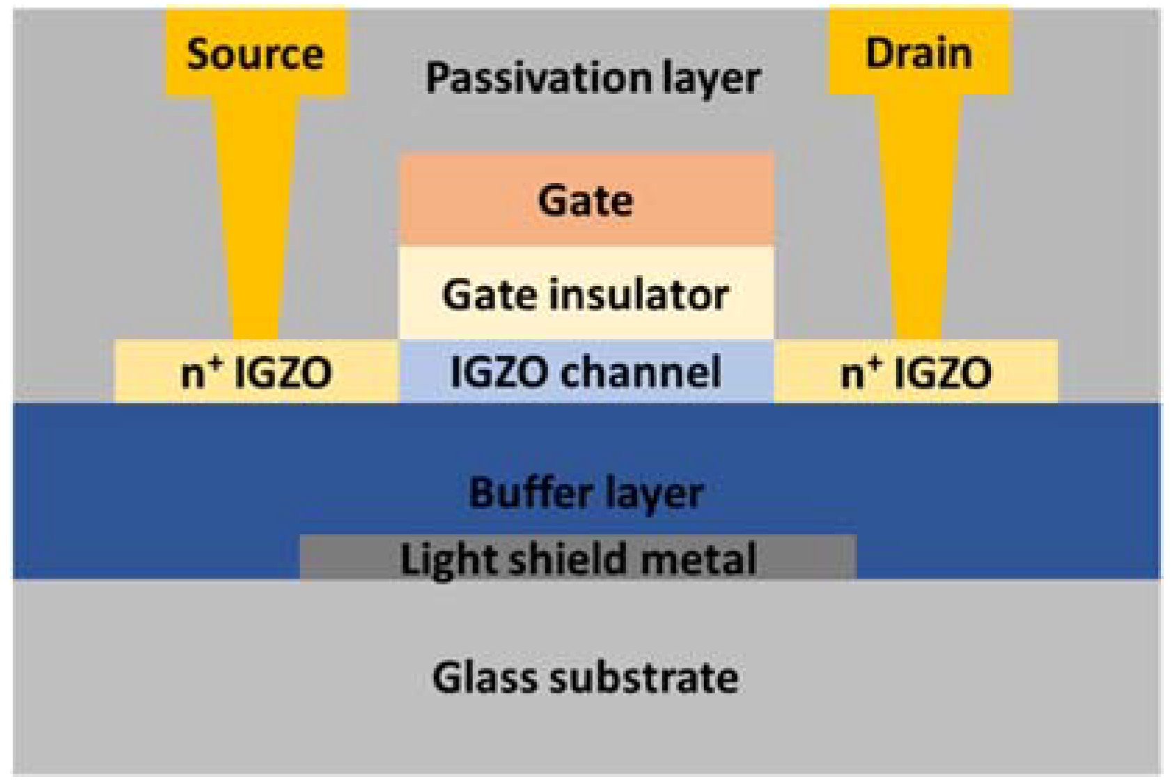
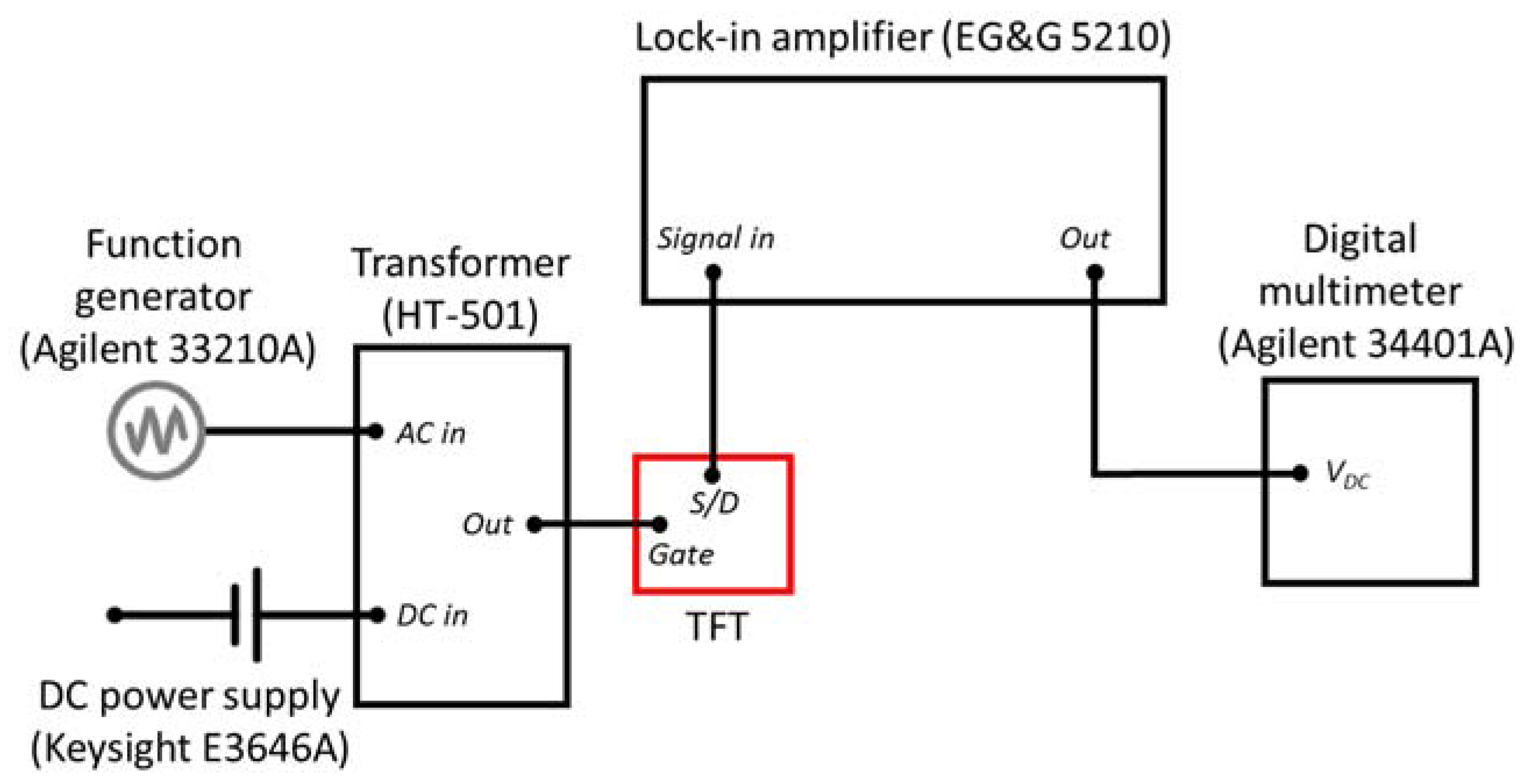
2. Experimental
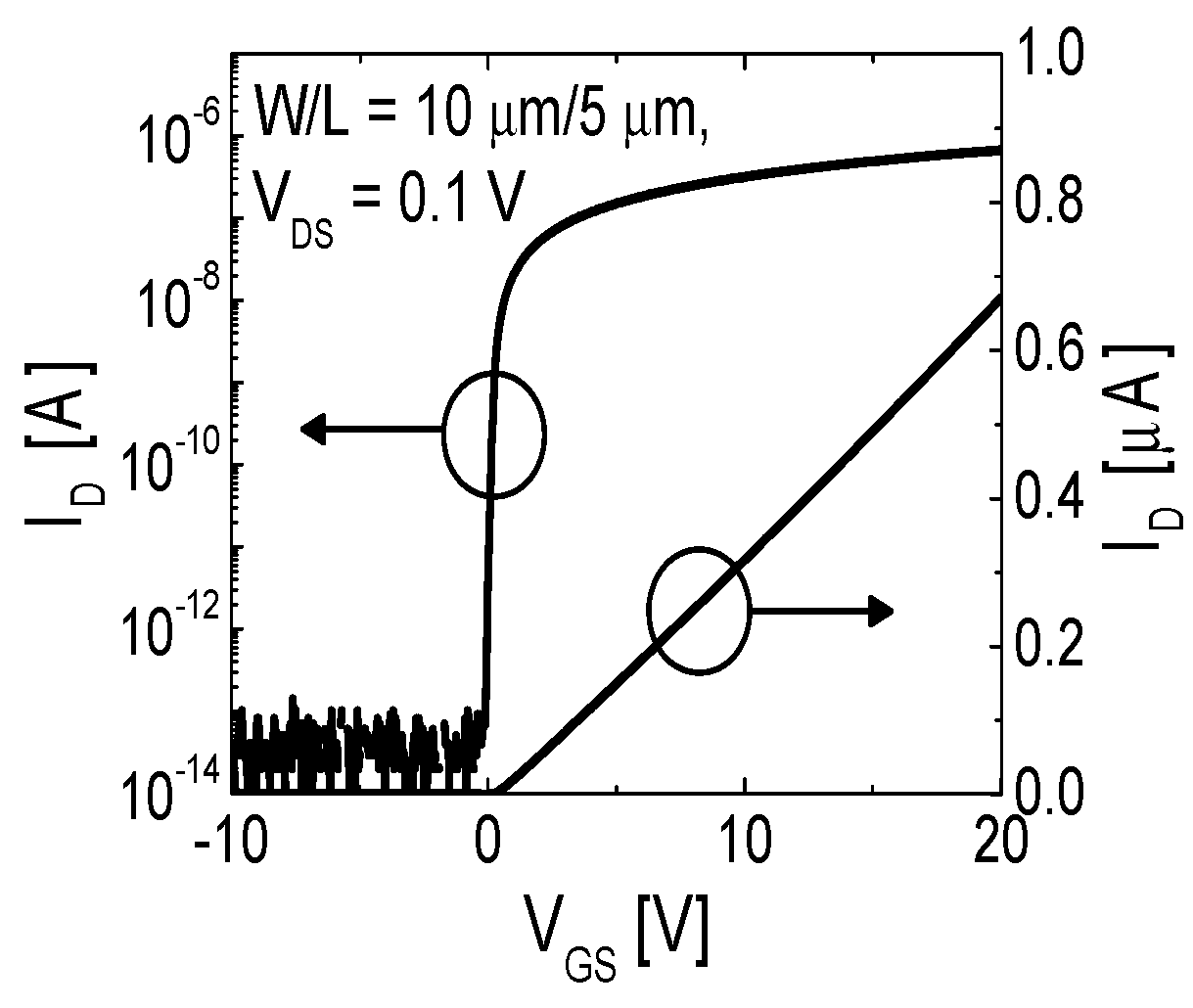
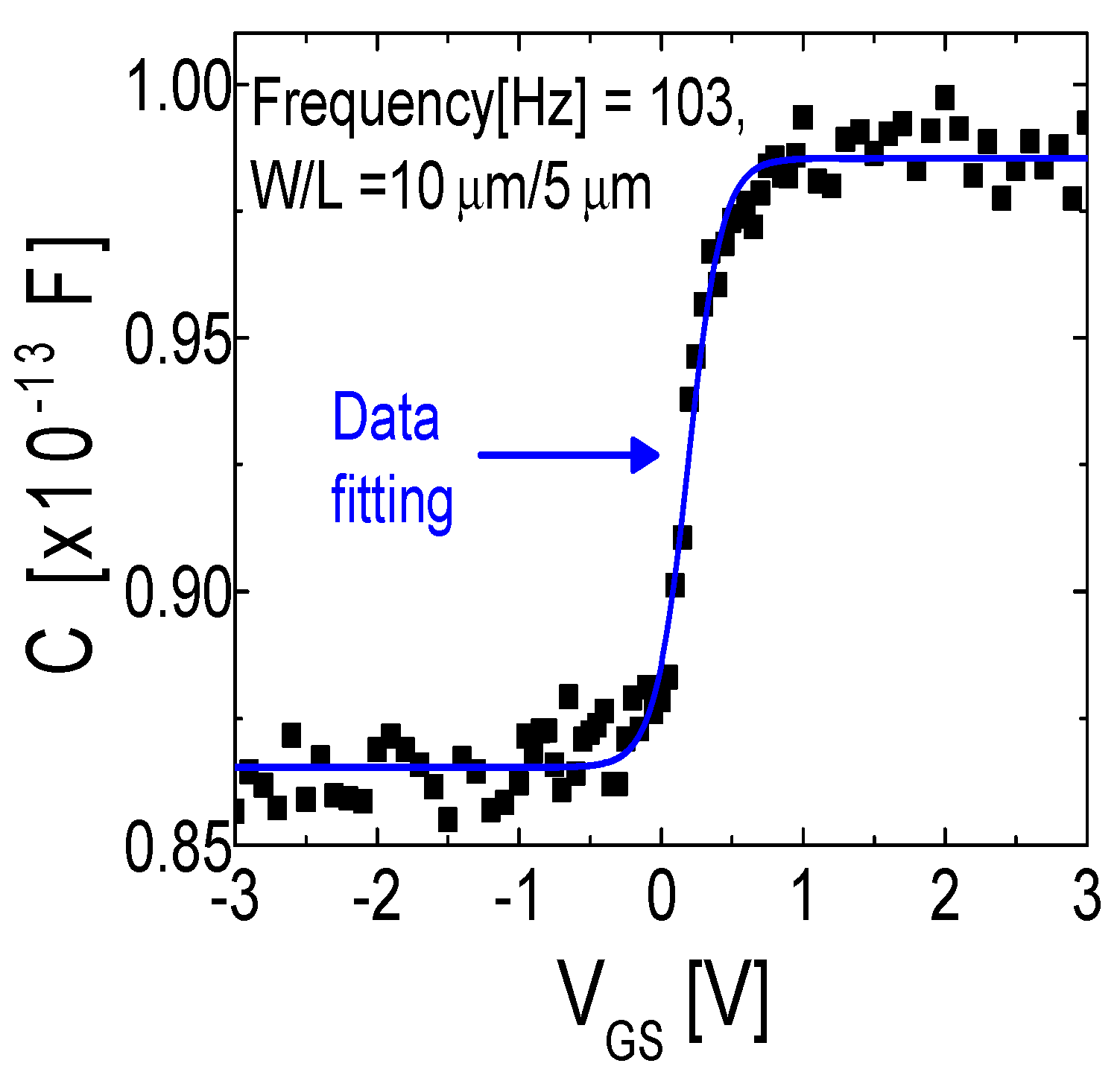
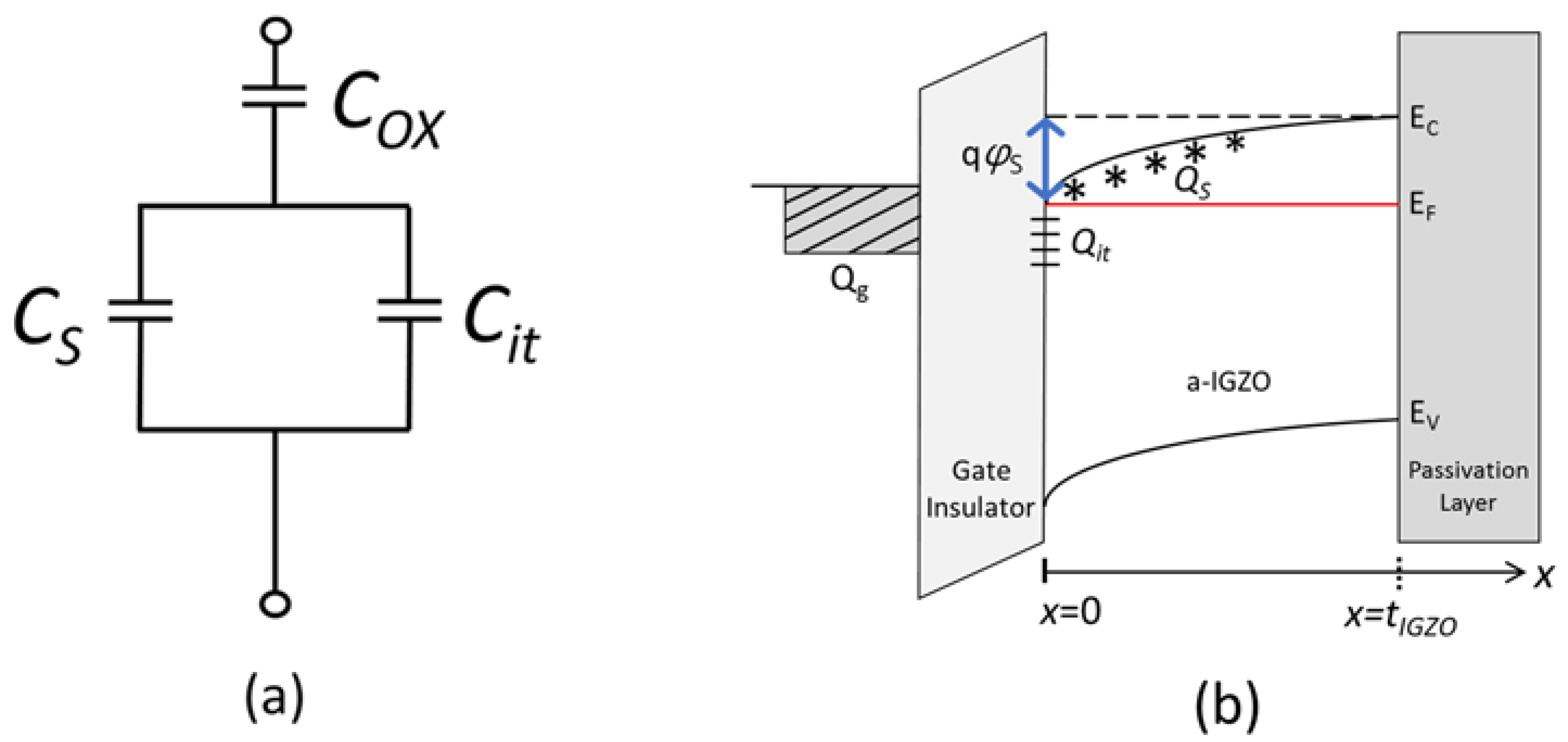
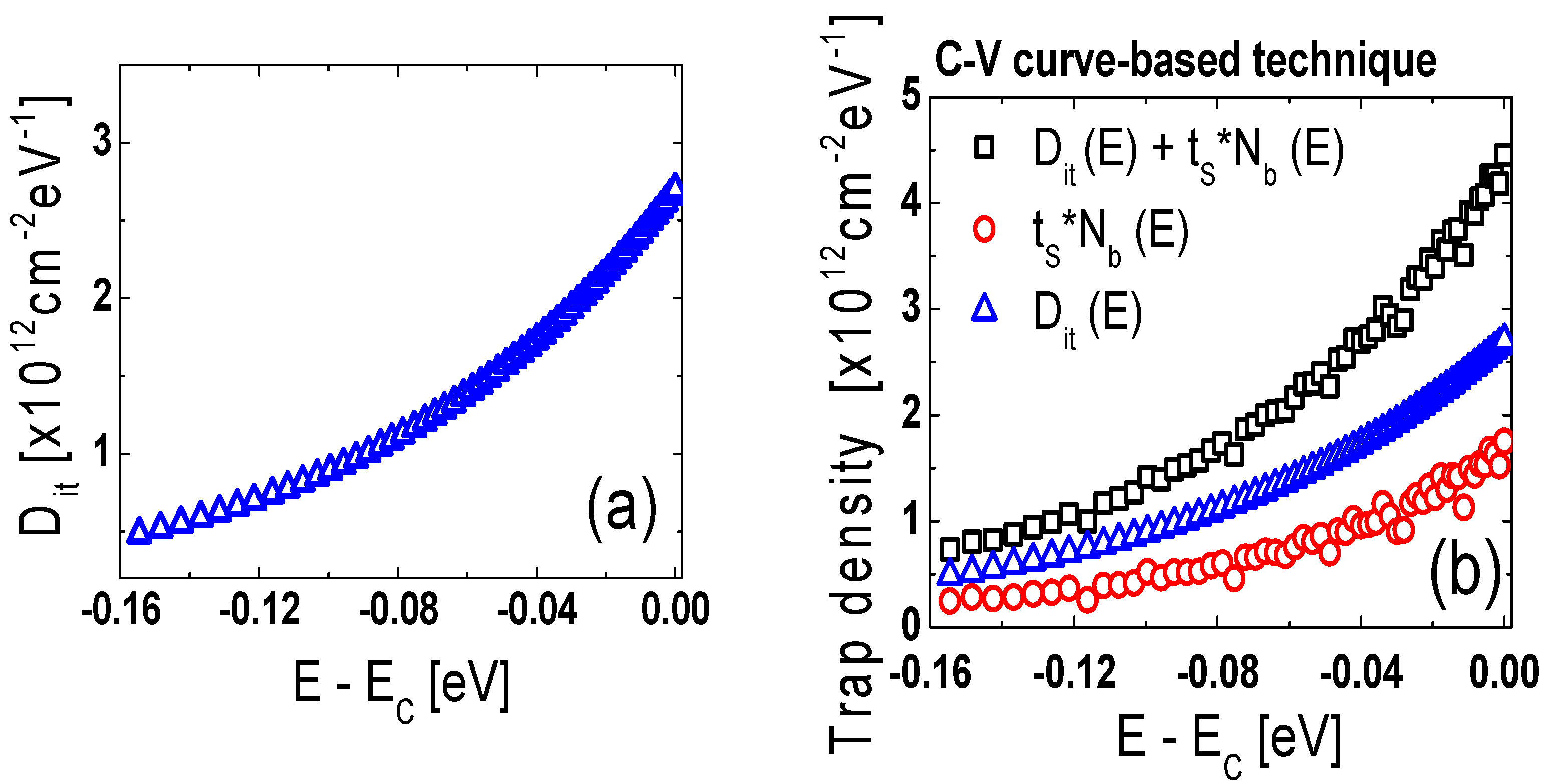
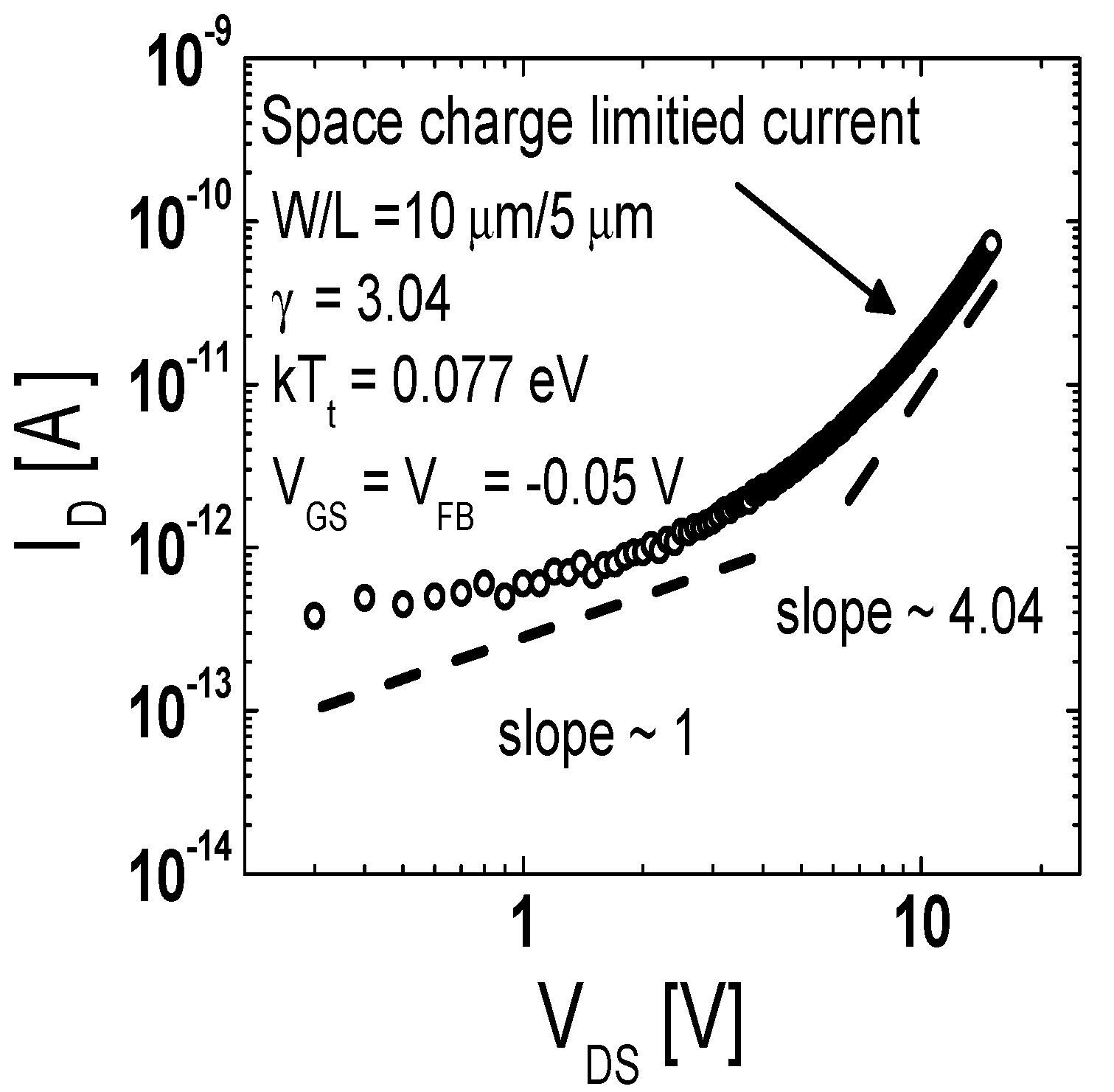
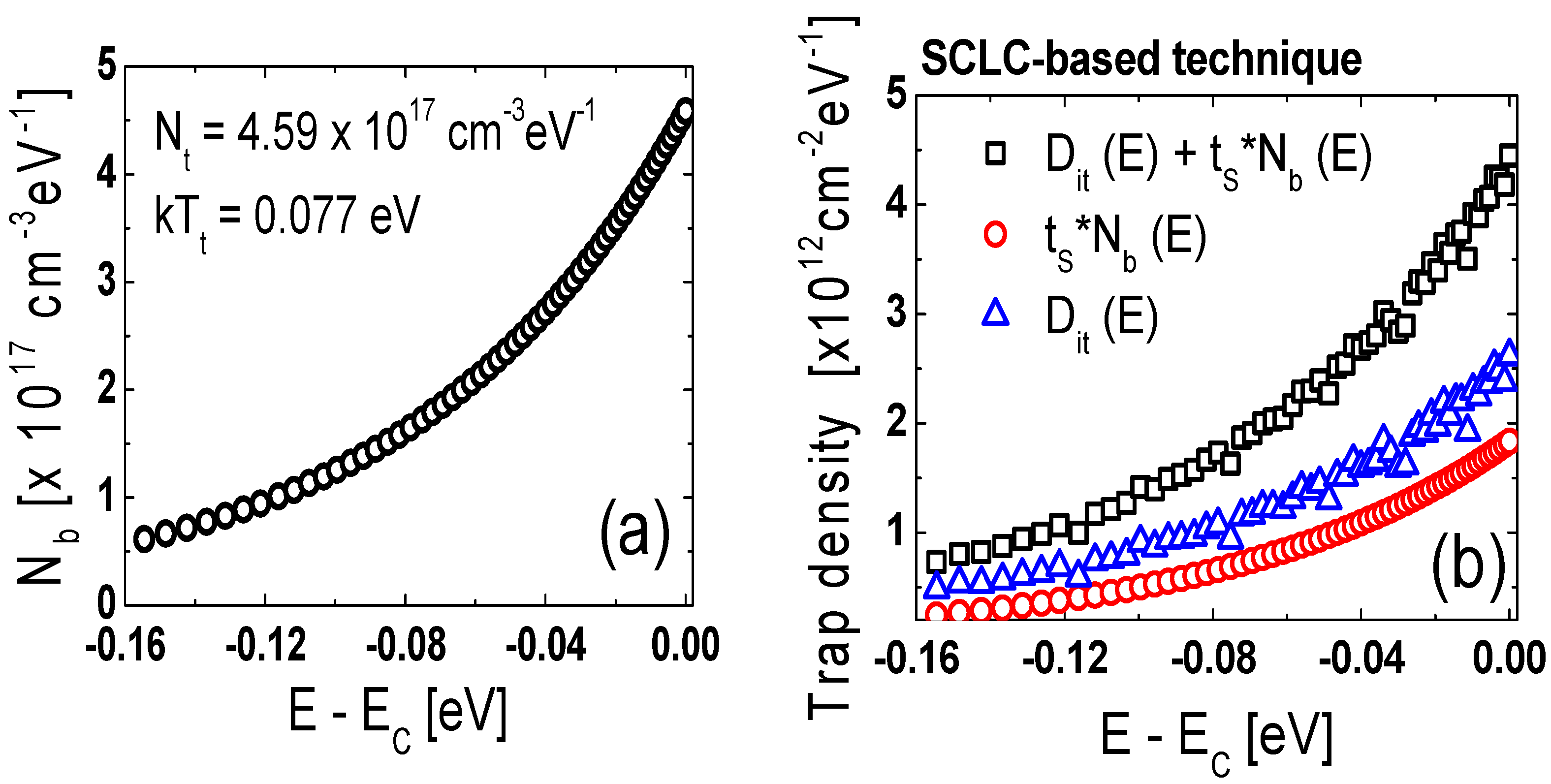
3. Results and Discussion
4. Conclusions
Author Contributions
Funding
Institutional Review Board Statement
Informed Consent Statement
Data Availability Statement
Conflicts of Interest
References
- Nomura, K.; Ohta, H.; Takagi, A.; Kamiya, T.; Hirano, M.; Hosono, H. Room-temperature fabrication of transparent flexible thin-film transistors using amorphous oxide semiconductors. Nature 2004, 432, 488. [Google Scholar] [CrossRef] [PubMed]
- Jeong, J.K.; Jeong, J.H.; Choi, J.H.; Im, J.S.; Kim, S.H.; Yang, H.W.; Kang, K.N.; Kim, K.S.; Ahn, T.K.; Chung, H.; et al. 3.1: Distinguished paper: 12.1-inch WXGA AMOLED display driven by indium-gallium-zinc oxide TFTs. In SID Symposium Digest of Technical Papers; Blackwell Publishing Ltd.: Oxford, UK, 2008; Volume 39, pp. 1–4. [Google Scholar]
- Mo, Y.G.; Kim, M.; Kang, C.K.; Jeong, J.H.; Park, Y.S.; Choi, C.G.; Kim, H.D.; Kim, S.S. Amorphous-oxide TFT backplane for large-sized AMOLED TVs. J. Soc. Inf. Disp. 2011, 19, 16–20. [Google Scholar] [CrossRef]
- Yu, E.K.H.; Jun, S.; Kim, D.H.; Kanicki, J. Density of states of amorphous In-Ga-Zn-O from electrical and optical characterization. J. Appl. Phys. 2014, 116, 154505. [Google Scholar] [CrossRef] [Green Version]
- De Jamblinne De Meux, A.; Pourtois, G.; Genoe, J.; Heremans, P. Defects in amorphous semiconductors: The case of amorphous indium gallium zinc oxide. Phys. Rev. Appl. 2018, 9, 54039. [Google Scholar] [CrossRef]
- Kimura, M.; Nakanishi, T.; Nomura, K.; Kamiya, T.; Hosono, H. Trap densities in amorphous-InGaZn O4 thin-film transistors. Appl. Phys. Lett. 2008, 92, 1–4. [Google Scholar] [CrossRef]
- Lee, S.; Ahnood, A.; Sambandan, S.; Madan, A.; Nathan, A. Analytical field-effect method for extraction of subgap states in thin-film transistors. IEEE Electron Device Lett. 2012, 33, 1006–1008. [Google Scholar] [CrossRef]
- Bae, M.; Yun, D.; Kim, Y.; Kong, D.; Jeong, H.K.; Kim, W.; Kim, J.; Hur, I.; Kim, D.H.; Kim, D.M. Differential ideality factor technique for extraction of subgap density of states in amorphous InGaZnO thin-film transistors. IEEE Electron Device Lett. 2012, 33, 399–401. [Google Scholar] [CrossRef]
- Chen, C.; Abe, K.; Kumomi, H.; Kanicki, J. Density of States of a-InGaZnO From Temperature-Dependent Field-Effect Studies. IEEE Trans. Electron Devices 2009, 56, 1177–1183. [Google Scholar] [CrossRef]
- Lee, S.; Park, S.; Kim, S.; Jeon, Y.; Jeon, K.; Park, J.H.; Park, J.; Song, I.; Kim, C.J.; Park, Y.; et al. Extraction of subgap density of states in amorphous ingazno thin-film transistors by using multifrequency capacitancevoltage characteristics. IEEE Electron Device Lett. 2010, 31, 231–233. [Google Scholar]
- Qiang, L.; Yao, R.H. A new extraction method of trap states in amorphous ingazno thin-film transistors. J. Disp. Technol. 2015, 11, 325–329. [Google Scholar] [CrossRef]
- Jeong, C.-Y.; Kim, H.-J.; Kim, J.I.; Lee, J.-H.; Kwon, H.-I. Extraction of bulk and interface trap densities in amorphous InGaZnO thin-film transistors. J. Vac. Sci. Technol. B Nanotechnol. Microelectron. Mater. Process. Meas. Phenom. 2016, 34, 060601. [Google Scholar] [CrossRef]
- Geng, D.; Kang, D.H.; Seok, M.J.; Mativenga, M.; Jang, J. High-Speed and Low-Voltage-Driven Shift Register With Self-Aligned Coplanar a -IGZO TFTs. IEEE Electron Device Lett. 2012, 33, 1012–1014. [Google Scholar] [CrossRef]
- Song, Z.; Wang, G.; Chen, J.; Gu, P.; Liu, F.; Xie, D.; Liu, W.; Sun, H.; Song, Y.S.; Yan, L.; et al. 24.4: High Performance Top-gate Self-aligned Coplanar a-IGZO TFTs with Light Shielding Metal Design. SID Symp. Dig. Tech. Pap. 2018, 49, 259–262. [Google Scholar] [CrossRef]
- Kim, J.B.; Lim, R.; Tsai, Y.C.; Wang, J.; Zhao, L.; Choi, S.Y.; Bender, M.; Yim, D.K. Highly stable self-aligned coplanar InGaZnO thin-film transistors and investigation on effective channel length. Dig. Tech. Pap.-SID Int. Symp. 2019, 50, 874–877. [Google Scholar] [CrossRef]
- Sayed, M.B. Solid-State Ac-Conductivity Analysis For The Long Debated Catalytic Activity Of The Boralite Sieve; Qatar University: Doha, Qatar, 1996. [Google Scholar]
- Park, J.S.; Jeong, J.K.; Mo, Y.G.; Kim, H.D.; Kim, S. Il Improvements in the device characteristics of amorphous indium gallium zinc oxide thin-film transistors by Ar plasma treatment. Appl. Phys. Lett. 2007, 90, 1–4. [Google Scholar] [CrossRef]
- Cultrera, A.; Tran, N.T.M.; D’Elia, V.; Ortolano, M.; Callegaro, L. Calibration of lock-in amplifiers in the low-frequency range. In Proceedings of the 23rd IMEKO TC4 International Symposium Electrical & Electronic Measurements Promote Industry 4.0, Xi’an, China, 17–20 September 2019; pp. 122–125. [Google Scholar]
- Wei, X.; Deng, W.; Fang, J.; Ma, X.; Huang, J. Determination of bulk and interface density of states in metal oxide semiconductor thin-film transistors by using capacitance-voltage characteristics. EPJ Appl. Phys. 2017, 80, 1–5. [Google Scholar] [CrossRef]
- Kim, D.H.; Park, M.J.; Kwon, H.I. Separate extraction of densities of interface and bulk trap states in high-mobility ZnON thin-film transistors. J. Nanoelectron. Optoelectron. 2017, 12, 1263–1266. [Google Scholar] [CrossRef]
- Bae, M.; Lee, K.M.; Cho, E.S.; Kwon, H.I.; Kim, D.M.; Kim, D.H. Analytical current and capacitance models for amorphous indium-gallium-zinc-oxide thin-film transistors. IEEE Trans. Electron Devices 2013, 60, 3465–3473. [Google Scholar] [CrossRef]
- Fung, T.-C. Amorphous In-Ga-Zn-O Thin Film Transistor for Future Optoelectronics. Ph.D. Thesis, University of Michigan, Ann Arbor, MI, USA, 2010. [Google Scholar]
- Jun, S.; Jo, C.; Bae, H.; Choi, H.; Kim, D.H.; Kim, D.M. Unified subthreshold coupling factor technique for surface potential and subgap density-of-states in amorphous thin film transistors. IEEE Electron Device Lett. 2013, 34, 641–643. [Google Scholar] [CrossRef]
- Fuh, C.S.; Liu, P.T.; Huang, W.H.; Sze, S.M. Effect of annealing on defect elimination for high mobility amorphous indium-zinc-tin-oxide thin-film transistor. IEEE Electron Device Lett. 2014, 35, 1103–1105. [Google Scholar] [CrossRef]
- Kim, H.J.; Kim, D.H.; Jeong, C.Y.; Lee, J.H.; Kwon, H.I. Determination of interface and bulk trap densities in high-mobility p-type WSe2 thin-film transistors. IEEE Electron Device Lett. 2017, 38, 481–484. [Google Scholar] [CrossRef]
- Kwan, C.P.; Street, M.; Mahmood, A.; Echtenkamp, W.; Randle, M.; He, K.; Nathawat, J.; Arabchigavkani, N.; Barut, B.; Yin, S.; et al. Space-charge limited conduction in epitaxial chromia films grown on elemental and oxide-based metallic substrates. AIP Adv. 2019, 9, 055018. [Google Scholar] [CrossRef] [Green Version]
- Shin, Y.S.; Lee, K.; Kim, Y.R.; Lee, H.; Lee, I.M.; Kang, W.T.; Lee, B.H.; Kim, K.; Heo, J.; Park, S.; et al. Mobility Engineering in Vertical Field Effect Transistors Based on Van der Waals Heterostructures. Adv. Mater. 2018, 30, 1–8. [Google Scholar] [CrossRef] [PubMed]


Publisher’s Note: MDPI stays neutral with regard to jurisdictional claims in published maps and institutional affiliations. |
© 2021 by the authors. Licensee MDPI, Basel, Switzerland. This article is an open access article distributed under the terms and conditions of the Creative Commons Attribution (CC BY) license (https://creativecommons.org/licenses/by/4.0/).
Share and Cite
Lee, D.-H.; Kim, D.-H.; Jeong, H.-S.; Hwang, S.-H.; Lee, S.; Kim, M.-H.; Lim, J.H.; Kwon, H.-I. Comparative Study on the Separate Extraction of Interface and Bulk Trap Densities in Indium Gallium Zinc Oxide Thin-Film Transistors Using Capacitance–Voltage and Current–Voltage Characteristics. Coatings 2021, 11, 1135. https://doi.org/10.3390/coatings11091135
Lee D-H, Kim D-H, Jeong H-S, Hwang S-H, Lee S, Kim M-H, Lim JH, Kwon H-I. Comparative Study on the Separate Extraction of Interface and Bulk Trap Densities in Indium Gallium Zinc Oxide Thin-Film Transistors Using Capacitance–Voltage and Current–Voltage Characteristics. Coatings. 2021; 11(9):1135. https://doi.org/10.3390/coatings11091135
Chicago/Turabian StyleLee, Dong-Ho, Dae-Hwan Kim, Hwan-Seok Jeong, Seong-Hyun Hwang, Sunhee Lee, Myeong-Ho Kim, Jun Hyung Lim, and Hyuck-In Kwon. 2021. "Comparative Study on the Separate Extraction of Interface and Bulk Trap Densities in Indium Gallium Zinc Oxide Thin-Film Transistors Using Capacitance–Voltage and Current–Voltage Characteristics" Coatings 11, no. 9: 1135. https://doi.org/10.3390/coatings11091135