Article

Effects of Oxygen Content on Operational Characteristics and Stability of High-Mobility IGTO Thin-Film Transistors during Channel Layer Deposition

School of Electrical and Electronics Engineering, Chung-Ang University, Seoul 06972, Korea
*
Authors to whom correspondence should be addressed.
Coatings 2021, 11(6), 698; https://doi.org/10.3390/coatings11060698
Submission received: 13 May 2021 / Revised: 31 May 2021 / Accepted: 8 June 2021 / Published: 10 June 2021
(This article belongs to the Special Issue New Advances in Thin-Film Transistor)

Abstract

:
In this study, we investigated the effects of oxygen content on the transfer characteristics and stability of high-mobility indium-gallium-tin oxide (IGTO) thin-film transistors (TFTs) during channel layer deposition. The IGTO thin films were deposited through direct current sputtering at different ambient oxygen percentages of 10%, 20%, 30%, 40%, and 50%. The experimental results indicate that the drain currents were hardly modulated by the gate-to-source voltage in the IGTO TFT prepared at 10% ambient oxygen. However, as the oxygen content increased from 20% to 50%, the transfer curves shifted to the positive direction with a decrease in field-effect mobility (μFE). The IGTO TFTs exhibited deteriorated positive bias stress (PBS) stability as the oxygen content increased. However, the stabilities of the IGTO TFTs under negative bias illumination stress (NBIS) improved with an increase in the ambient oxygen percentage during the channel layer deposition. Furthermore, to understand the mechanism of the observed phenomena, we performed X-ray photoelectron spectroscopy (XPS) analysis of the IGTO thin films prepared at different oxygen percentages. The XPS results demonstrate that the deteriorated PBS stability and enhanced NBIS stability of the IGTO TFTs prepared at higher oxygen percentages were mainly ascribed to the larger amount of oxygen interstitials resulting from the excess oxygen and the smaller number of oxygen vacancies within the IGTO, respectively. The obtained results suggest that the oxygen percentages of 30% in the sputtering ambient is the most suitable oxygen percentage for optimizing the electrical properties (μFE = 24.2 cm2/V·s, subthreshold swing = 0.43 V/dec, and threshold voltage = −2.2 V) and adequate PBS and NBIS stabilities of IGTO TFTs.

1. Introduction

Since the inceptive report on indium-gallium-zinc oxide (IGZO) thin-film transistors (TFTs) published by Nomura et al. in 2004, IGZO TFTs have attracted significant research interest, owing to their excellent electrical characteristics, high uniformity, and low fabrication costs. IGZO TFTs are widely used as the backplanes of large-area flat-panel displays, including active-matrix organic light-emitting diode (AMOLED) displays [1,2,3]. However, the field- effect mobility (μFE) of IGZO TFTs is approximately 10 cm2/V·s, which is insufficient to meet the requirements of high-frame-rate and ultra-high-resolution next-generation displays. Over the past decade, various oxide TFTs with higher field-effect mobilities than those of IGZO TFTs have been extensively studied for next-generation display applications. Among these oxide thin film transistors (TFTs), indium-gallium-tin oxide (IGTO) TFTs have attracted significant attention as promising oxide TFTs that can replace conventional indium-gallium-zinc oxide (IGZO) TFTs [4,5,6]. In IGTO, the cation Sn is alloyed instead of conventional Zn because the spatial overlap between the 5 s orbitals of In and Sn is larger than that of In and Zn. The efficient formation of the percolation pathway for electron conduction results in a higher field-effect mobility (μFE = ~20–40 cm2/V·s) in the IGTO TFTs than in the conventional IGZO TFTs (μFE = ~10 cm2/V·s) [7]. Furthermore, the IGTO TFTs exhibited excellent electrical characteristics even at low annealing temperatures of less than 200 °C. Generally, AOS TFTs require the use of relatively high annealing temperatures above 300 °C in order to stimulate their electrical properties [8,9]. however, such temperature limits the application of oxide for flexible electronic devices since most cost-effective flexible substrates (PET, PEN, PC, PS, PP) are deteriorated at this temperature because of low melting point [10]. Thus, the IGTO TFT is a promising backplane device for flexible display applications. Jeong et al. examined the effects of annealing temperature on the electrical characteristics and stability of IGTO TFTs [11,12]. Kim et al. investigated the effects of chamber pressure on the electrical properties and reliability of IGTO TFTs, and Jeong et al. studied the influence of the annealing atmosphere on the electrical characteristics of IGTO TFTs [13,14]. Although the oxygen content has been reported to strongly affect the electrical characteristics of oxide TFTs with various channel materials, limited studies have focused on the effects of oxygen content on the electrical performance of IGTO TFTs during channel layer deposition [15,16,17,18,19]. Oh et al. examined the influence of oxygen partial pressure during sputtering on the transfer characteristics and electrical stability of IGTO TFTs [20]. They reported that the electrical stabilities of IGTO TFTs under positive bias stress (PBS) degraded with an increase in the oxygen partial pressure during sputtering. Additionally, the deteriorated PBS stabilities of IGTO TFTs prepared at higher oxygen partial pressures were attributed to a larger number of interface electron trap states originating from the oxygen vacancies (VO). However, considering that VO is mainly related to the negative bias illumination stress (NBIS) stability in IGZO and IGTO TFTs, it is necessary to examine whether this interpretation is accurate [21,22,23,24,25,26,27,28]. Consequently, in this study, we examined the effects of oxygen content on the transfer characteristics and stabilities of high-mobility IGTO TFTs during channel layer deposition. A systematic study was conducted to determine the physical mechanisms responsible for the observed effects of varying oxygen content on the transfer characteristics and PBS/NBIS stabilities of the IGTO TFTs during channel layer deposition.

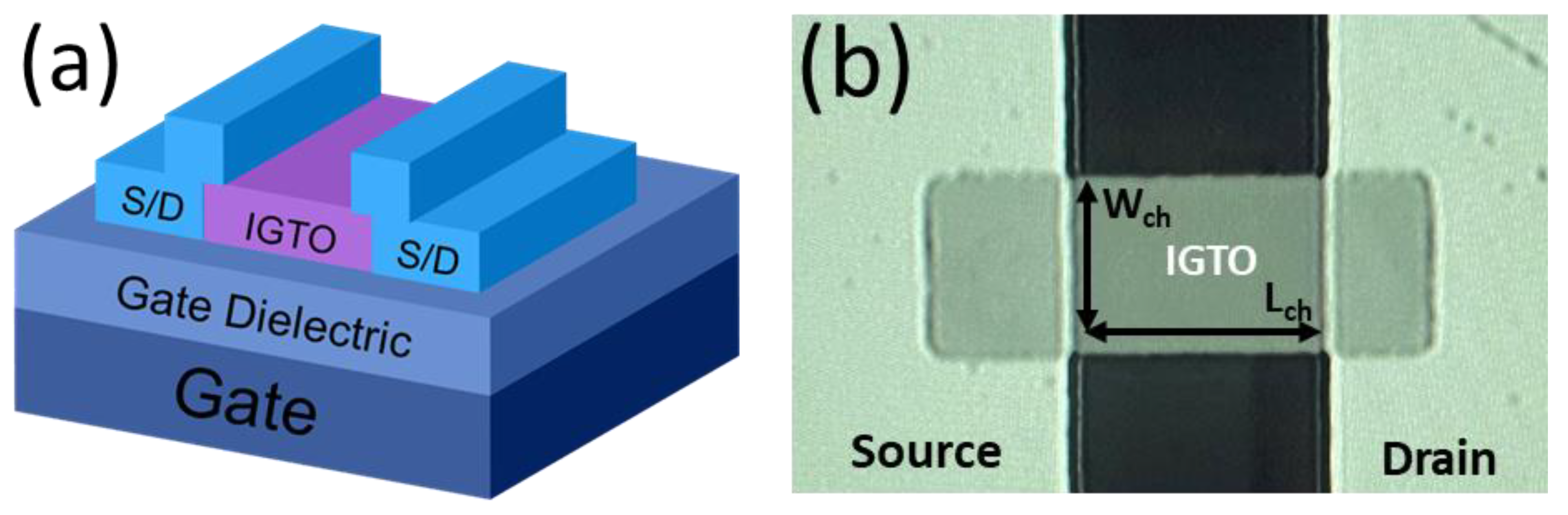
2. Experimental Details

Bottom-gate and top-contact structure IGTO TFTs were employed in this study. A heavily doped p-type silicon wafer and 100 nm-thick thermal SiO2 were used as the gate electrode and gate insulator, respectively. The active layer and source/drain electrode were patterned using photolithography and lift-off processes. First, the photoresist (AZ5214E, AZ Electronic Materials, Somerville, NJ, USA) was spin-coated onto SiO2 at 4000 rpm for 40 s and soft-baked at 95 °C for 90 s. Then, UV light was directed through a photomask onto the sample for 4.4 s to generate active layer patterns. next, photoresist was developed with a AZ MIF300 developer (AZ electronic Materials, Somerville, NJ, USA) for 30 s after the sample hard-baked at 120 °C for 120 s. The uncovered regions were subsequently deposited with IGTO thin film of 20 nm thickness via direct current (DC) magnetron sputtering at various gas flow rates (Ar:O2 = 35:3.9, 35:8.8, 35:15, 35:23.4, and 35:35 sccm) and oxygen percentages (10%, 20%, 30%, 40%, and 50%). Finally, the photoresist was lifted off by soaking the sample in acetone to obtain the active layer patterns. All sputtering processes were performed under the working pressure of 3 mTorr using a 3”-diameter IGTO target without substrate heating. Subsequently, the source and drain electrode patterns were also patterned on the active layer by the same photolithography and lift-off process, and a 100-nm-thick indium-tin oxide layer was formed for the source and drain electrodes of the IGTO TFTs using DC magnetron sputtering. Finally, the IGTO TFTs were subjected to thermal annealing at 180 °C for 1 h in air. Figure 1a,b display the schematic view and optical image of the fabricated IGTO TFTs, respectively.
Electrical measurements were conducted inside a vacuum chamber to avoid the effects of ambient air on the electrical characteristics of the TFTs using a precision semiconductor parameter analyzer (Agilent 4156C, Agilent, Santa Clara, CA, USA) at room temperature. The chemical states of the IGTO thin films formed under different oxygen partial pressures were investigated using X-ray photoelectron spectroscopy (XPS; K-alpha+, Thermo Scientific-KR, Seoul, Korea) near the IGTO/SiO2 interface.

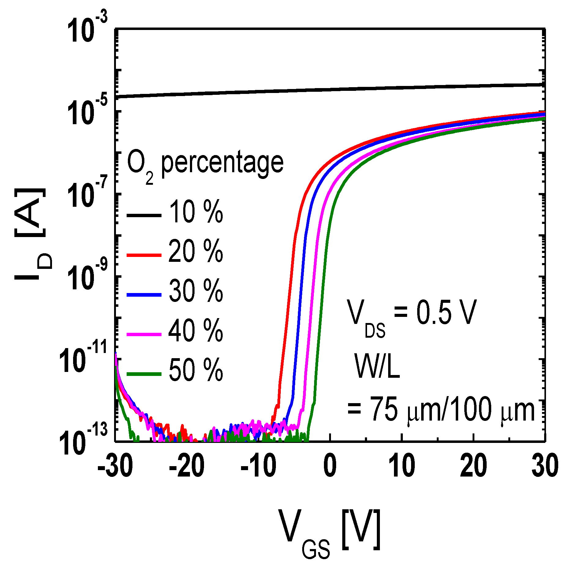
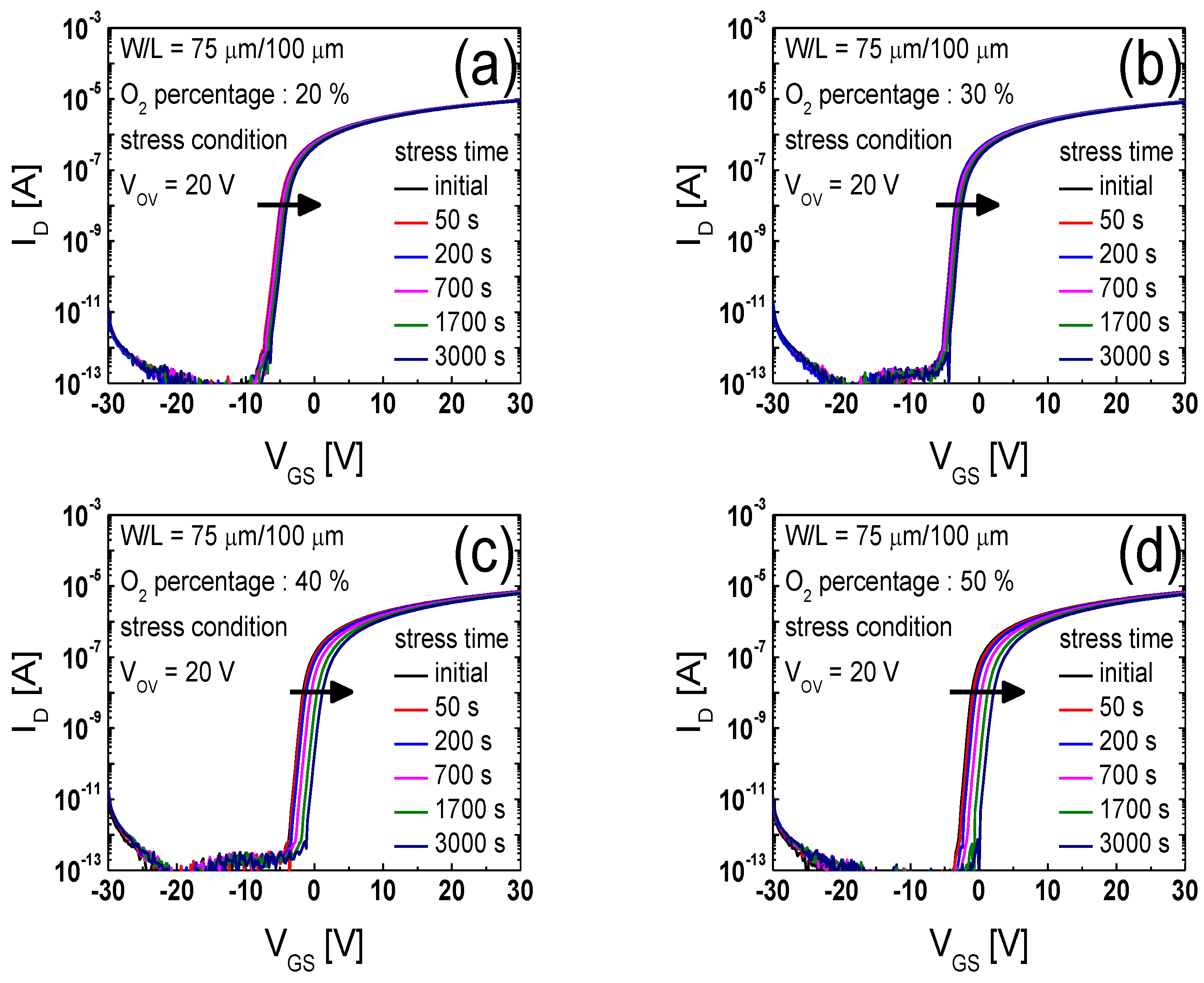
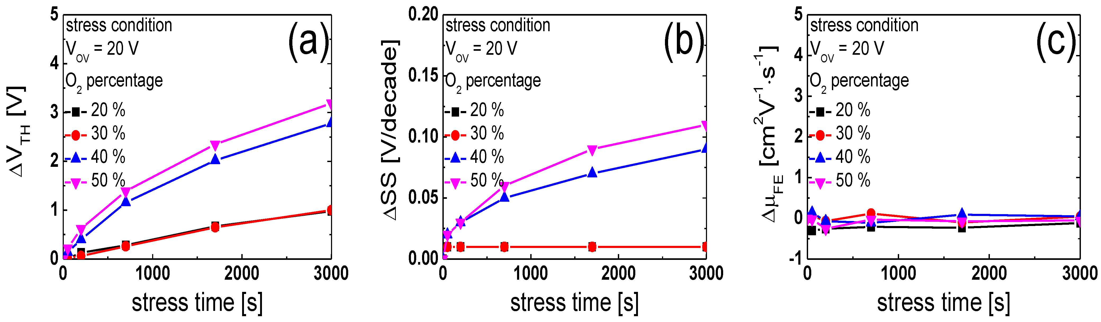
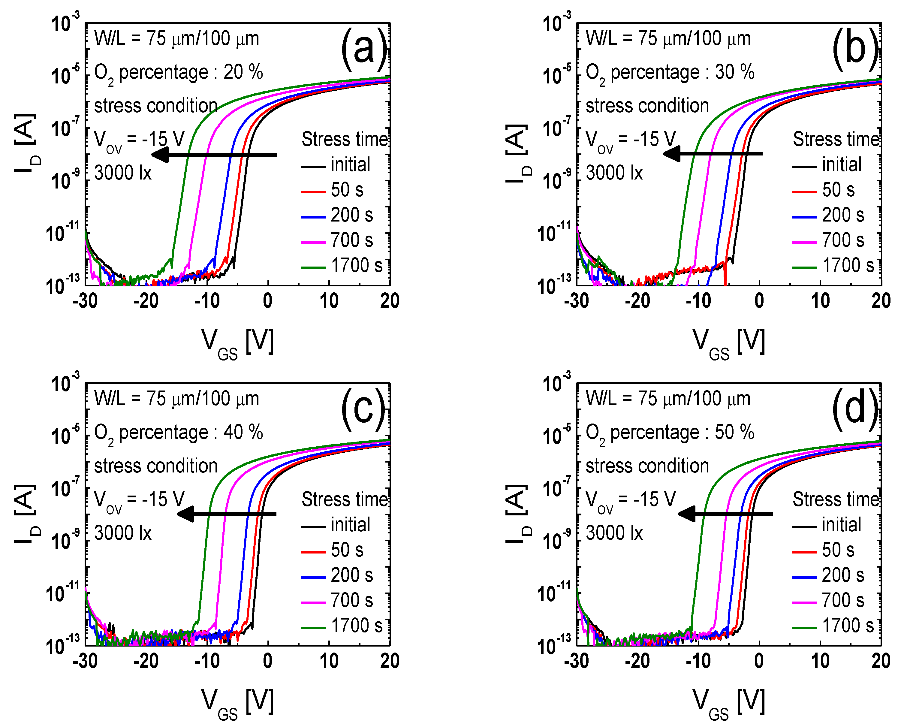
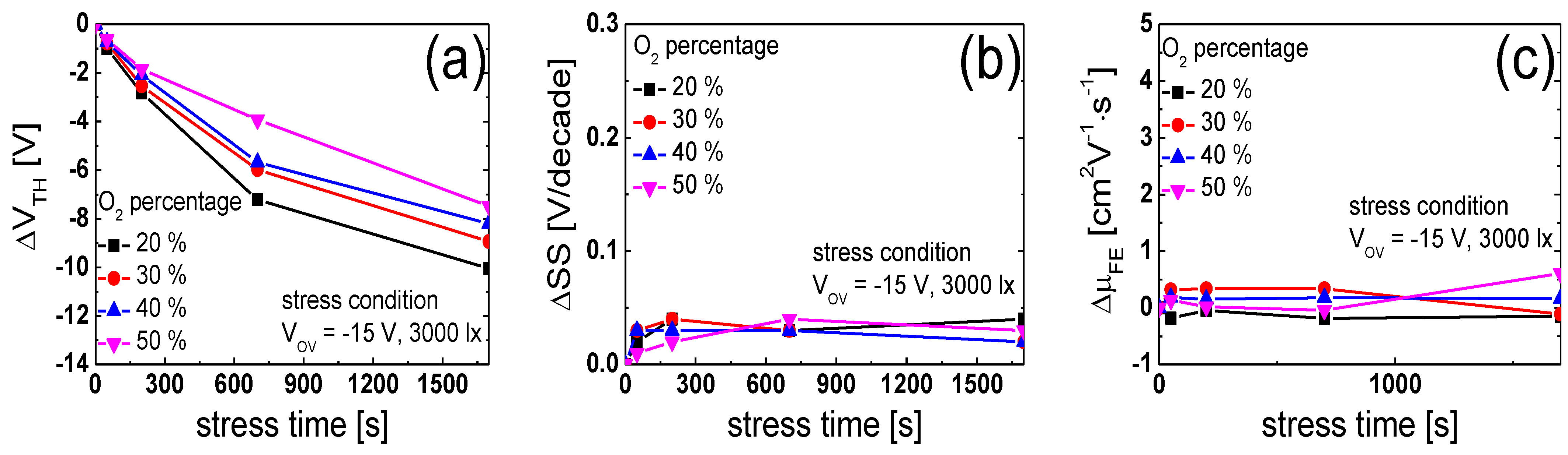
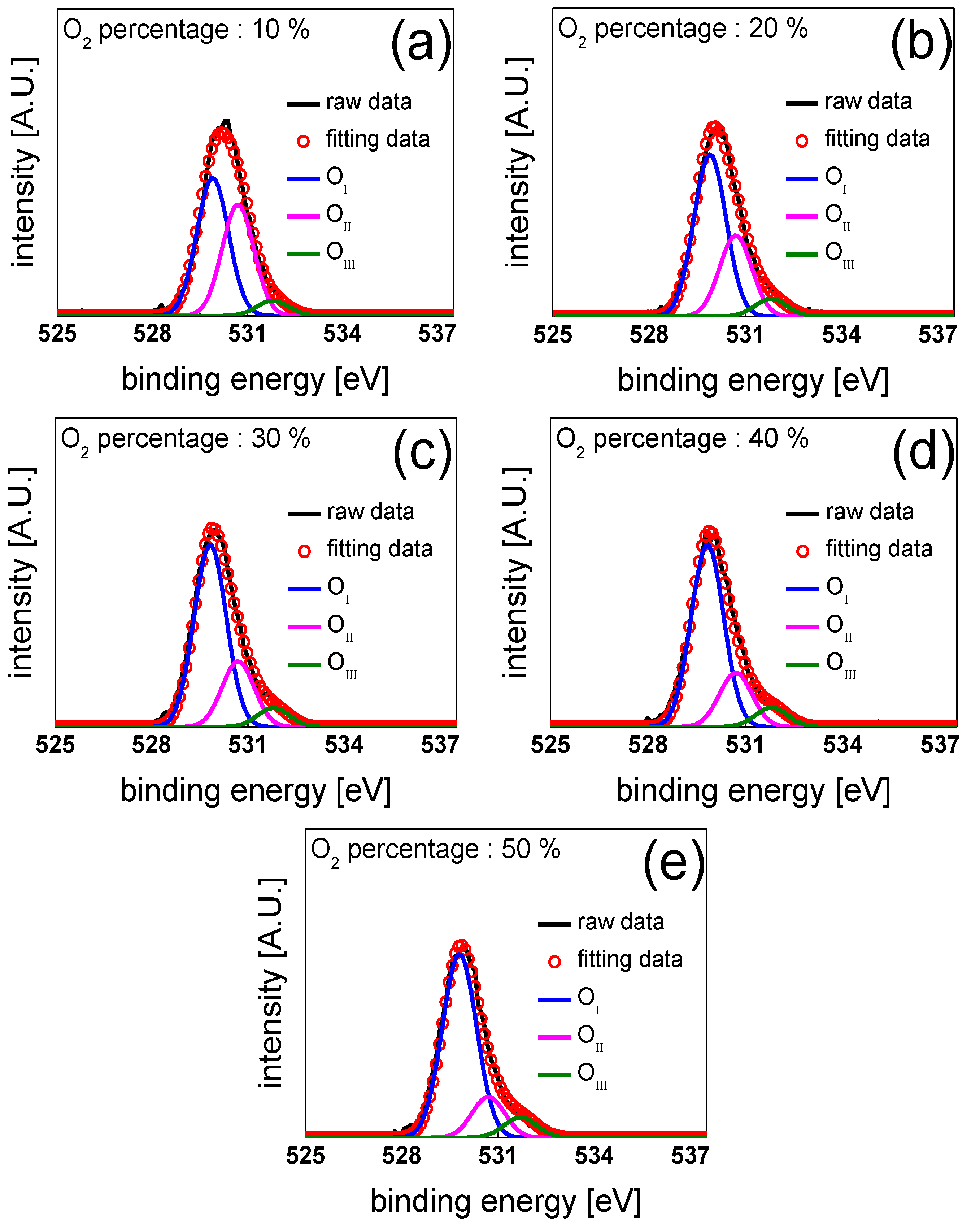
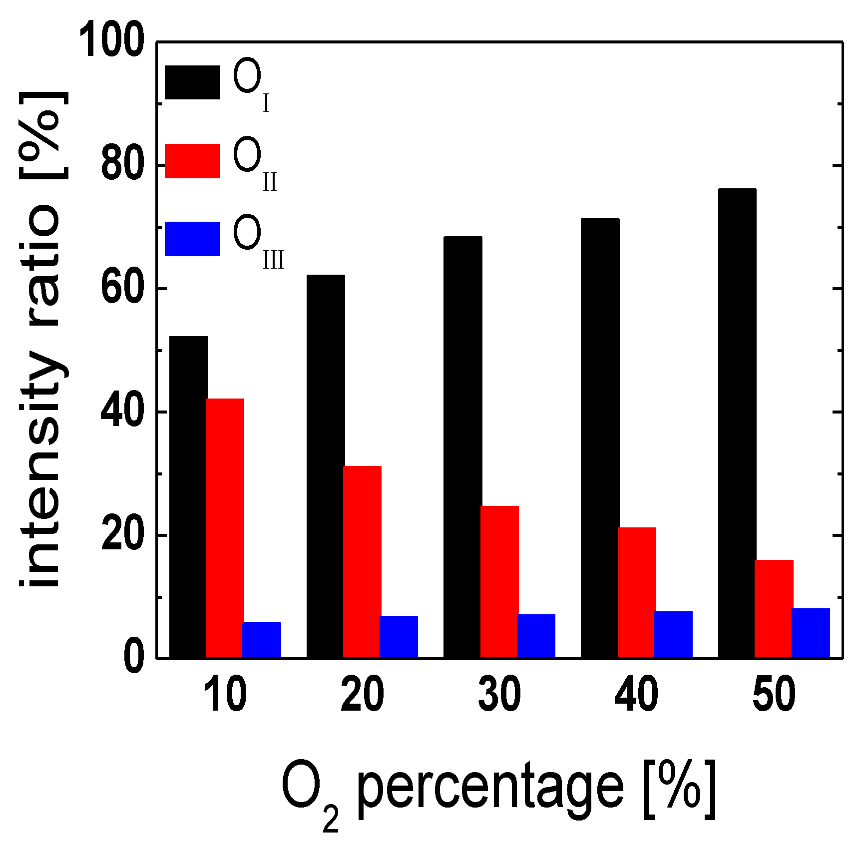
3. Results and Discussion

Figure 2 shows the transfer curves of the IGTO TFTs prepared at the different oxygen percentages of 10%, 20%, 30%, 40%, and 50% in the sputtering ambient, where VGS, VDS, and ID are the gate-to-source voltage, drain-to-source voltage, and drain current, respectively. Measurements were performed for the TFTs with the channel width/length (W/L) of 75 μm/100 μm, wherein VGS was varied from −30 to 30 V at a fixed VDS of 0.5 V. As evident from Figure 2, ID is hardly modulated by VGS in the IGTO TFT prepared at 10% oxygen.
Table 1 summarizes the electrical parameters obtained from the IGTO TFTs prepared at different oxygen percentages, where μFE was calculated using the maximum transconductance at VDS = 0.5 V and the threshold voltage (VTH) was defined as the VGS value causing ID = W/L × 10−8 A. The subthreshold swing (SS) was determined as the dVGS/dlogID value in the range of 10−10 < ID < 10−9 A. As evident from Figure 2 and Table 1, VTH increased but µFE decreased as the oxygen percentage increased from 20% to 50%. The SS exhibited the lowest value in the IGTO TFT prepared at 30% oxygen.
Figure 3a–d show the time evolutions of the transfer curves under a constant overdrive voltage (VOV = VGS − VTH) of 20 V measured from the IGTO TFTs prepared at the different oxygen contents of 20%, 30%, 40%, and 50% in the sputtering ambient, respectively. As can be seen in Figure 3a–d, the transfer curves shifted in the positive direction with an increase in the stress time in all the TFTs.
Furthermore, Figure 4a–c illustrate the time dependence of the threshold voltage shift (ΔVTH) and that of the variation in the SS (ΔSS) and μFE (ΔμFE) values obtained from the IGTO TFTs prepared at different oxygen percentages in PBS after every stress time. Figure 4a shows that ΔVTH in the IGTO TFTs prepared at 40% (ΔVTH = 2.78 V after 3000 s) and 50% (ΔVTH = 3.19 V after 3000 s) oxygen exhibited significantly larger values than those in the IGTO TFTs prepared at oxygen contents of 20% (ΔVTH = 0.98 V after 3000 s) and 30% (ΔVTH = 1.00 V after 3000 s).
Moreover, Figure 4b shows that the SS value hardly changed after an application of stress in the IGTO TFTs prepared at the oxygen percentages of 20% and 30%. However, it increased after applying stresses in the IGTO TFTs prepared at 40% (ΔSS = 0.09 V/dec after 3000 s) and 50% (ΔSS = 0.1 V/dec after 3000 s) oxygen. The ΔμFE values remained nearly unchanged during the stresses in all the TFTs.
In the previous studies on oxide thin films and TFTs, the instability of electrical properties under PBS can be explained by two general mechanisms: (1) the charge trapping model and (2) the defect creation model. In the charge trapping model, VTH shifts to the positive direction without degradation of SS. It is widely believed that the ΔVTH is contributed by charges trapped at the dielectric/channel interface and inside the bulk of the channel, resulting in ΔVTH without a significant change in SS. In the defect creation model, on the other hand, VTH shifts to the positive direction with degradation of SS. as a result of gate bias stress that induces formation of trap sites [29,30]. Therefore, as can be seen in Figure 3 and Figure 4, one can infer the creation of defects in the a-IGTO thin films prepared at 40% and 50% oxygen contents under PBS.
Figure 5a–d show the time evolutions of the transfer curves under the constant VOV of −15 V with light illumination (brightness = 3000 lx) measured from the IGTO TFTs prepared at different oxygen contents of 20%, 30%, 40%, and 50% in the sputtering ambient, respectively. As evident from Figure 5a–d, the transfer curves shifted in the negative direction with an increase in the stress time in all the TFTs. Figure 6a–c illustrate the time dependences of the ΔVTH, ΔSS, and ΔμFE values obtained from the IGTO TFTs prepared at the different oxygen percentages under NBIS after every stress time. Figure 6a–c show that the magnitude of NBIS-induced ΔVTH decreases with an increase in the oxygen percentages in the sputtering ambient. However, there is no significant variation in the SS and μFE values during NBIS in all IGTO TFTs.
In the previous studies on oxide thin films and TFTs, the negative VTH shift in the NBIS condition was attributed to: (1) the photo-induced hole trapping, (2) photo-transition from VO to VO2+ (here, the VO and VO2+ denote the oxygen vacancy with the neutral and +2 charge states, respectively) and (3) photo-desorption of O2 on the channel surface. The hole trapping model assumes that photo-generated hole carriers are trapped at the gate dielectric/channel interfacial trap sites or gate dielectric bulk film. Therefore, the hole trapping phenomena depend strongly on the gate dielectric layer, which might not be responsible for the difference of oxygen contents in the sputtering ambient. A more plausible mechanism would involve the oxygen vacancy concentration in the a-IGTO film. Previously, oxide material has been reported to suffer from photoconductivity phenomena, which can be explained by the photon-activated transition of neutral oxygen vacancies, VO, to the VO2+ charged state. Because such a photo-transition leads two delocalized free electrons into the conduction band, VTH shifts to the negative direction [31,32]. The Figure 5 and Figure 6 supports such a hypothesis. Finally, since the NBIS was measured in vacuum, the photo-desorption of O2 effect was excluded.
To evaluate the physical mechanisms for the effects of varying oxygen content on the electrical properties and stabilities of the IGTO TFTs, as observed in Figure 2, Figure 3, Figure 4, Figure 5 and Figure 6, the IGTO thin films prepared at different oxygen percentages were analyzed via XPS. Figure 7a–e show the O 1s core-level XPS results of the IGTO thin films prepared at the different oxygen percentages of 10%, 20%, 30%, 40%, and 50%, respectively. The O 1s XPS results were deconvoluted into three peaks (OI, OII, and OIII) using the Gaussian function, where their origins are the lattice oxygen (OI), VO (OII), and the weakly bonded excess oxygen or the hydroxyl group (OIII), respectively. The positions of each peak are 529.8 ± 0.1 (peak OI), 530.7 ± 0.1 (peak OII), and 531.8 ± 0.1 (peak OIII) eV [14]. Figure 8 shows the XPS peak area ratios corresponding to OI, OII, and OIII, obtained from the IGTO thin films prepared at different oxygen contents in the sputtering ambient. Figure 8 shows that the XPS peak area ratio of OIII continuously increased with an increase in the oxygen percentage, implying that the higher area ratio of OIII in the IGTO thin films prepared at higher oxygen percentages is probably due to the larger number of weakly bonded excess oxygen atoms within the IGTO thin films [33,34]. In IGZO or IGTO, the weakly bonded excess oxygen is easily ionized to the oxygen interstitials (Ois) owing to the low formation energy, where Oi creates acceptor-like sub-gap states near the conduction band (CB) edge [35,36,37]. The acceptor-like sub-gap states above the mid-gap increase SS, enhance electron trapping and the μFE remains unchanged during PBS in n-type oxide TFTs. Therefore, the high SS, and poor PBS stability of the IGTO TFTs prepared at 40% and 50% oxygen can be ascribed to the relatively high concentrations of Oi within the IGTO channel layer. Furthermore, the formation of Oi from the weakly bonded excess oxygen is accelerated under PBS in IGZO or IGTO TFTs, which is believed to be the reason for the increase in the SS values after PBS in IGTO TFTs prepared at 40% and 50% ambient oxygen. In addition, Figure 8 shows that the XPS peak area ratio of OII continuously decreased as the oxygen percentage increased. It is well known that VO creates shallow and deep donor states within n-type oxide semiconductors, such as IGZO or IGTO [38,39]. The ionized shallow donors provide free electrons to the CB; therefore, the concentration of free electrons increases as the concentration of VO increases within the IGTO. The increase in the free electron concentration facilitates the formation of a percolation conduction path in multi-cation n-type oxide semiconductors. Therefore, the low value of VTH and the high values of μFE obtained as the oxygen percentage decreased [40,41]. Therefore, a higher μFE value and lower VTH value of the IGTO TFTs prepared at lower oxygen percentages can be attributed to the higher concentrations of VO within the IGTO active layer.
In addition, a higher carrier concentration within the active layer increases the SS value of the TFT, which is considered to be the reason for the high SS value in the IGTO TFTs prepared at the oxygen percentage of 20%. Under NBIS, VO is ionized to VO2+, which moves toward the channel/gate insulator interface in n-type oxide TFTs such as IGZO or IGTO TFTs. The formation of the VO2+ accumulation layer close to the gate insulator and an increased free electron concentration within the channel layer result in shifting of the transfer curves of n-type oxide TFTs in the negative direction [23]. The results in Figure 8 demonstrate that the poorer NBIS stability of the IGTO TFTs prepared at lower oxygen percentages can be ascribed to the higher concentrations of VO within the IGTO channel layer compared with the IGTO TFTs prepared at higher oxygen percentages. The experimental results in Figure 2, Figure 3, Figure 4, Figure 5, Figure 6 and Figure 7 indicate the importance of determining the appropriate oxygen content during channel layer deposition in IGTO TFTs to optimize the transfer characteristics and PBS/NBIS stabilities of the devices. Although it is necessary to further improve the electrical performances of TFTs, the TFT prepared at the oxygen percentage of 30% exhibited the best electrical characteristics (μFE = 24.2 cm2/V·s, SS = 0.43 V/dec., and VTH = −2.2 V) and adequate PBS and NBIS stabilities among the fabricated IGTO TFTs.

4. Conclusions

In this study, we investigated the effects of oxygen content in the sputtering ambient on the transfer characteristics and stabilities of IGTO TFTs using devices prepared at the oxygen contents of 10%, 20%, 30%, 40%, and 50%. The experimental results showed that an increase in the oxygen percentage during the channel layer deposition increased VTH and decreased the µFE value of the fabricated IGTO TFTs. Furthermore, it was observed that the electrical stability in PBS deteriorated with an increase in the oxygen percentage. However, the NBIS stability of the TFT enhanced as the oxygen percentage increased. The XPS analysis results revealed that the VTH increase and µFE decreased as the oxygen percentage increased from 20% to 50% due to decreased oxygen vacancy. Furthermore, the deteriorated PBS stability and the improved NBIS stability of the IGTO TFTs prepared at higher oxygen percentages were due to the increase in the amount of excess oxygen oriented Oi and VO within the IGTO active layer. The obtained results demonstrated that the optimum oxygen percentage in the sputtering ambient for the IGTO TFT is approximately 30%, producing a low SS, acceptably high µFE, and adequate PBS/NBIS stabilities of IGTO TFTs.

Author Contributions

Conceptualization, H.-S.J., H.-S.C. and H.-I.K.; experiment, H.-S.J., S.-H.H. and D.-H.L.; data analysis, H.-S.J. and H.-I.K., writing—original draft preparation, H.-S.J.; supervision, S.-H.S. and H.-I.K.; writing—review and editing, H.-I.K. All authors have read and agreed to the published version of the manuscript.

Funding

This research was supported by a National Research Foundation of Korea (NRF) grant funded by the Korean government (MSIT) (No. 2020R1A2B5B01001765) and the Chung-Ang University Research Scholarship Grants in 2020. The authors would like to thank Shinhyuk Kang (Samsung Corning Advanced Glass) for supporting the IGTO sputter target for this work.

Institutional Review Board Statement

Not applicable.

Informed Consent Statement

Not applicable.

Data Availability Statement

Data is contained within the article.

Conflicts of Interest

The authors declare no conflict of interest.

References

  1. Nomura, K.; Ohta, H.; Takagi, A.; Kamiya, T.; Hirano, M.; Hosono, H. Room-temperature fabrication of transparent flexible thin-film transistors using amorphous oxide semiconductors. Nature 2004, 432, 488–492. [Google Scholar] [CrossRef]
  2. Yabuta, H.; Sano, M.; Abe, K.; Aiba, T.; Den, T.; Kumomi, H.; Nomura, K.; Kamiya, T.; Hosono, H. High mobility thin-film transistor with amorphous InGaZnO4 channel fabricated by room temperature rf magnetron sputtering. Appl. Phys. Lett. 2006, 89, 112123. [Google Scholar] [CrossRef]
  3. Suresh, A.; Muth, J.F. Bias stress stability of indium gallium zinc oxide channel based transparent thin film transistors. Appl. Phys. Lett. 2008, 92, 033502. [Google Scholar] [CrossRef] [Green Version]
  4. Cha, H.-S.; Jeong, H.-S.; Hwang, S.-H.; Lee, D.-H.; Kwon, H.-I. Electrical performance and stability improvements of high-mobility indium–gallium–tin oxide thin-film transistors using an oxidized aluminum capping layer of optimal thickness. Electronics 2020, 9, 2196. [Google Scholar] [CrossRef]
  5. Shin, M.-G.; Hwang, S.-H.; Cha, H.-S.; Jeong, H.-S.; Kim, D.-H.; Kwon, H.-I. Effects of proton beam irradiation on the physical and chemical properties of IGTO thin films with different thicknesses for thin-film transistor applications. Surf. Interfaces 2021, 23, 100990. [Google Scholar] [CrossRef]
  6. Kim, B.K.; On, N.; Choi, C.H.; Kim, M.J.; Kang, S.; Lim, J.H.; Jeong, J.K. Polycrystalline indium gallium tin oxide thin-film transistors with high mobility exceeding 100 cm2/Vs. IEEE Electron. Device Lett. 2021, 42, 347–350. [Google Scholar] [CrossRef]
  7. Lee, J.; Kim, D.; Lee, S.; Cho, J.; Park, H.; Jang, J. High field effect mobility, amorphous In-Ga-Sn-O thin-film transistor with no effect of negative bias illumination stress. IEEE Electron. Device Lett. 2019, 40, 1443–1446. [Google Scholar] [CrossRef]
  8. Kang, Y.H.; Jeong, S.; Ko, J.M.; Lee, J.Y.; Choi, Y.; Lee, C.; Cho, S.Y. Two-component solution processing of oxide semiconductors for thin-film transistors via self-combustion reaction. J. Mater. Chem. C 2014, 2, 4247–4256. [Google Scholar] [CrossRef]
  9. Tak, Y.J.; Yoon, D.H.; Yoon, S.; Choi, U.H.; Sabri, M.M.; Ahn, B.; Kim, H.J. Enhanced electrical characteristics and stability via simultaneous ultraviolet and thermal treatment of passivated amorphous In-Ga-Zn-O thin-film transistors. ACS Appl. Mater. Interfaces 2014, 6, 6399–6405. [Google Scholar] [CrossRef] [PubMed]
  10. Liu, C.; Sun, Y.; Qin, H.; Liu, Y.; Wei, S.; Zhao, Y. Low-temperature, high-performance InGaZnO thin-film transistors fabricated by capacitive coupled plasma-assistant magnetron sputtering. IEEE Electron. Device Lett. 2019, 40, 415–418. [Google Scholar] [CrossRef]
  11. Jeong, H.-J.; Ok, K.-C.; Park, J.; Lim, J.; Cho, J.; Park, J.-S. Stability improvement of In–Sn–Ga–O thin-film transistors at low annealing temperatures. IEEE Electron. Device Lett. 2015, 36, 1160–1162. [Google Scholar] [CrossRef]
  12. Jeong, H.-J.; Lee, H.-M.; Oh, K.-T.; Park, J.; Park, J.-S. Enhancement of In-Sn-Ga-O TFT performance by the synergistic combination of UV + O3 radiation and low temperature annealing. J. Electroceram. 2016, 37, 158–162. [Google Scholar] [CrossRef]
  13. Kim, H.-A.; Kim, J.O.; Hur, J.S.; Son, K.-S.; Lim, J.H.; Cho, J.; Jeong, J.K. Achieving high mobility in IGTO thin-film transistors at a low temperature via film densification. IEEE Trans. Electron. Devices 2018, 65, 4854–4860. [Google Scholar] [CrossRef]
  14. Jeong, H.-S.; Cha, H.S.; Hwang, S.H.; Kwon, H.-I. Effects of annealing atmosphere on electrical performance and stability of high-mobility indium-gallium-tin oxide thin-film transistors. Electronics 2020, 9, 1875. [Google Scholar] [CrossRef]
  15. Wu, G.; Sahoo, A.K. Influence of oxygen flow rate on channel width dependent electrical properties of indium gallium zinc oxide thin-film transistors. Nanomaterials 2020, 10, 2357. [Google Scholar] [CrossRef]
  16. Hsu, M.-H.; Chang, S.-P.; Chang, S.-J.; Wu, W.-T.; Li, J.-Y. Oxygen partial pressure impact on characteristics of indium titanium zinc oxide thin film transistor fabricated via RF sputtering. Nanomaterials 2017, 7, 156. [Google Scholar] [CrossRef] [Green Version]
  17. Choi, S.; Kim, J.-Y.; Kang, H.; Ko, D.; Rhee, J.; Choi, S.-J.; Kim, D.M.; Kim, D.H. Effect of oxygen content on current stress-induced instability in bottom-gate amorphous InGaZnO thin-film transistors. Materials 2019, 12, 3149. [Google Scholar] [CrossRef] [PubMed] [Green Version]
  18. Furuta, M.; Kamada, Y.; Kimura, M.; Hiramatsu, T.; Matsuda, T.; Furuta, H.; Li, C.; Fujita, S.; Hirao, T. Analysis of hump characteristics in thin-film transistors with ZnO channels deposited by sputtering at various oxygen partial pressures. IEEE Electron. Device Lett. 2010, 31, 1257–1259. [Google Scholar] [CrossRef] [Green Version]
  19. Lestari, A.D.; Putri, M.; Heo, Y.-W.; Lee, H.Y. Influence of oxygen partial pressure on radio frequency magnetron sputtered amorphous InZnSnO thin film transistors. J. Nanosci. Nanotechnol. 2020, 20, 252–256. [Google Scholar] [CrossRef]
  20. Oh, C.; Jang, H.; Kim, H.W.; Jung, H.; Park, H.; Cho, J.; Kim, B.S. Influence of oxygen partial pressure in In-Sn-Ga-O thin-film transistors at a low temperature. J. Alloys Compd. 2019, 805, 211–217. [Google Scholar] [CrossRef]
  21. Ji, K.H.; Kim, J.-I.; Jung, H.Y.; Park, S.Y.; Choi, R.; Kim, U.K.; Hwang, C.S.; Lee, D.; Hwang, H.; Jeong, J.K. Effect of high-pressure oxygen annealing on negative bias illumination stress-induced instability of InGaZnO thin film transistors. Appl. Phys. Lett. 2011, 98, 103509. [Google Scholar] [CrossRef]
  22. Song, J.H.; Oh, N.; Du Anh, B.; Kim, H.D.; Jeong, J.K. Dynamics of threshold voltage instability in IGZO TFTs: Impact of high pressurized oxygen treatment on the activation energy barrier. IEEE Trans. Electron. Devices 2016, 63, 1054–1058. [Google Scholar] [CrossRef]
  23. Mativenga, M.; Um, J.G.; Jang, J. Reduction of bias and light instability of mixed oxide thin-film transistors. Appl. Sci. 2017, 7, 885. [Google Scholar] [CrossRef] [Green Version]
  24. Huang, X.; Zhou, D.; Xu, W. Influence of N2/O2 partial pressure ratio during channel layer deposition on the temperature and light stability of a-InGaZnO TFTs. Appl. Sci. 2019, 9, 1880. [Google Scholar] [CrossRef] [Green Version]
  25. Wang, D.; Furuta, M.; Tomai, S.; Yano, K. Impact of photo-excitation on leakage current and negative bias instability in InSnZnO thickness-varied thin-film transistors. Nanomaterials 2020, 10, 1782. [Google Scholar] [CrossRef]
  26. Zhang, Y.; Xie, H.; Dong, C. Electrical performance and bias-stress stability of amorphous InGaZnO thin-film transistors with buried-channel layers. Micromachines 2019, 10, 779. [Google Scholar] [CrossRef] [PubMed] [Green Version]
  27. Kim, J.-H.; Park, E.-K.; Kim, M.S.; Cho, H.J.; Lee, D.-H.; Kim, J.-H.; Khang, Y.; Park, K.C.; Kim, Y.-S. Bias and illumination instability analysis of solution-processed a-InGaZnO thin-film transistors with different component ratios. Thin Solid Films 2018, 645, 154–159. [Google Scholar] [CrossRef]
  28. Chen, J.; Huang, X.; Li, Q.; Fang, Z.; Ning, H.; Tao, R.; Liang, H.; Zhou, Y.; Yao, R.; Peng, J. All-sputtering, high-transparency, good-stability coplanar top-gate thin film transistors. Appl. Sci. 2019, 9, 83. [Google Scholar] [CrossRef] [Green Version]
  29. Park, H.; Nam, Y.; Jin, J.; Bae, B.S. Improvement of bias stability of oxyanion-incorporated aqueous sol–gel processed indium zinc oxide TFTs. J. Mater. Chem. C. 2014, 2, 5998–6003. [Google Scholar] [CrossRef]
  30. Jin, J.W.; Nathan, A.; Barquinha, P.; Pereira, L.; Fortunato, E.; Martins, R.; Cobb, B. Interpreting anomalies observed in oxide semiconductor TFTs under negative and positive bias stress. AIP Adv. 2016, 6, 085321. [Google Scholar] [CrossRef]
  31. Ji, K.H.; Kim, J.-I.; Jung, H.Y.; Park, S.Y.; Choi, R.; Mo, Y.G.; Jeong, J.K. Comprehensive studies of the degradation mechanism in amorphous InGaZnO transistors by the negative bias illumination stress. Microelectron. Eng. 2011, 88, 1412–1416. [Google Scholar] [CrossRef]
  32. Hung, M.P.; Wang, D.; Toda, T.; Jiang, J.; Furuta, M. Quantitative analysis of hole-trapping and defect-creation in InGaZnO thin film transistors under negative-bias illumination-stress. ECS J. Solid State Sci. Technol. 2014, 3, 3023–3026. [Google Scholar] [CrossRef]
  33. Ji, H.; Hwang, A.Y.; Lee, C.K.; Yun, P.S.; Bae, J.U.; Park, K.-S.; Jeong, J.K. Improvement in field-effect mobility of indium zinc oxide transistor by titanium metal reaction method. IEEE Trans. Electron. Devices 2015, 62, 1009–1013. [Google Scholar] [CrossRef]
  34. Shin, Y.; Kim, S.T.; Kim, K.; Kim, M.Y.; Oh, S.; Jeong, J.K. The mobility enhancement of indium gallium zinc oxide transistors via low-temperature crystallization using a tantalum catalytic layer. Sci. Rep. 2017, 7, 10885. [Google Scholar] [CrossRef]
  35. Ide, K.; Kikuchi, Y.; Nomura, K.; Kimura, M.; Kamiya, T.; Hosono, H. Effects of excess oxygen on operation characteristics of amorphous In-Ga-Zn-O thin film transistors. Appl. Phys. Lett. 2011, 99, 093507-1–093507-3. [Google Scholar] [CrossRef]
  36. Zhou, X.; Shao, Y.; Zhang, L.; Lu, H.; He, H.; Han, D.; Wang, Y.; Zhang, S. Oxygen interstitial creation in a-IGZO thin-film transistors under positive gate-bias stress. IEEE Electron. Device Lett. 2017, 38, 1252–1255. [Google Scholar] [CrossRef]
  37. Omura, H.; Kumomi, H.; Nomura, K.; Kamiya, T.; Hirano, M.; Hosono, H. First-principles study of native point defects in crystalline indium gallium zinc oxide. J. Appl. Phys. 2020, 105, 093712. [Google Scholar] [CrossRef]
  38. Kamiya, T.; Nomura, K.; Hirano, M.; Hosono, H. Electronic structure of oxygen deficient amorphous oxide semiconductor a-InGaZnO4−x: Optical analyses and first-principle calculations. Phys. Stat. Solidi 2008, 5, 3098–3100. [Google Scholar] [CrossRef]
  39. Noh, H.-K.; Chang, K.J.; Ryu, B.; Lee, W.-J. Electronic structure of oxygen-vacancy defects in amorphous In-Ga-Zn-O semiconductors. Phys. Rev. B 2011, 84, 115205. [Google Scholar] [CrossRef]
  40. Yoon, J.; Jung, H.; Jang, J.T.; Lee, J.; Lee, Y.; Lim, M.; Kim, D.M.; Kim, D.H.; Choi, S.J. Hybrid complementary inverter based on carbon nanotube and IGZO thin-film transistors with controlled process conditions. J. Alloys Compd. 2018, 762, 456–462. [Google Scholar] [CrossRef]
  41. Oh, H.; Yoon, S.M.; Ryu, M.K.; Hwang, C.S.; Yang, S.; Park, S.H. Photon-accelerated negative bias instability involving subgap states creation in amorphous In–Ga–Zn–O thin film transistor. Appl. Phys. Lett. 2010, 97, 183502-1–183502-3. [Google Scholar] [CrossRef]
Figure 1. (a) Schematic view and (b) optical image of the fabricated IGTO TFTs prepared to examine the effects of varying oxygen content on the electrical characteristics of TFTs during channel layer deposition.
Coatings 11 00698 g001
Figure 2. Semi-logarithmic scale plot of the transfer curves measured from the IGTO TFTs (W/L = 75 μm/100 μm) prepared at oxygen contents of 10%, 20%, 30%, 40%, and 50% in the sputtering ambient.
Coatings 11 00698 g002
Figure 3. Time evolutions of the transfer curves under constant VOV of 20 V measured from the IGTO TFTs prepared at oxygen contents of (a) 20%, (b) 30%, (c) 40%, and (d) 50% in the sputtering ambient.
Coatings 11 00698 g003
Figure 4. Time dependences of (a) ΔVTH, (b) ΔSS, and (c) ΔμFE values obtained from the IGTO TFTs prepared at different oxygen percentages under PBS after every stress time.
Coatings 11 00698 g004
Figure 5. Time evolution of the transfer curves under constant VOV of −15 V with a light illumination (brightness = 3000 lx) measured from the IGTO TFTs prepared at the oxygen contents of (a) 20%, (b) 30%, (c) 40%, and (d) 50% in the sputtering ambient.
Coatings 11 00698 g005
Figure 6. Time dependences of (a) ΔVTH, (b) ΔSS, and (c) ΔμFE values obtained from the IGTO TFTs prepared at different oxygen percentages under NBIS after every stress time.
Coatings 11 00698 g006
Figure 7. O 1s core-level XPS results of the IGTO thin films prepared at the oxygen contents of (a) 10%, (b) 20%, (c) 30%, (d) 40%, and (e) 50%.
Coatings 11 00698 g007
Figure 8. XPS peak area ratios corresponding to OI, OII, and OIII, obtained from the IGTO thin films prepared at different oxygen percentages in the sputtering ambient.
Coatings 11 00698 g008
Table 1. Electrical parameters obtained from the IGTO TFTs prepared at the oxygen contents of 20%, 30%, 40%, and 50% in the sputtering ambient.
O2 Percentage (%)VTH (V)SS (V/dec.)μFE (cm2/V·s)
20−3.40.625.1
30−2.20.424.2
40−0.20.522.0
500.30.521.5
Publisher’s Note: MDPI stays neutral with regard to jurisdictional claims in published maps and institutional affiliations.

