
Annealing Effect on the Contact Angle, Surface Energy, Electric Property, and Nanomechanical Characteristics of Co40Fe40W20 Thin Films

 , ,
, ,
Abstract
:1. Introduction
2. Materials and Methods
3. Results
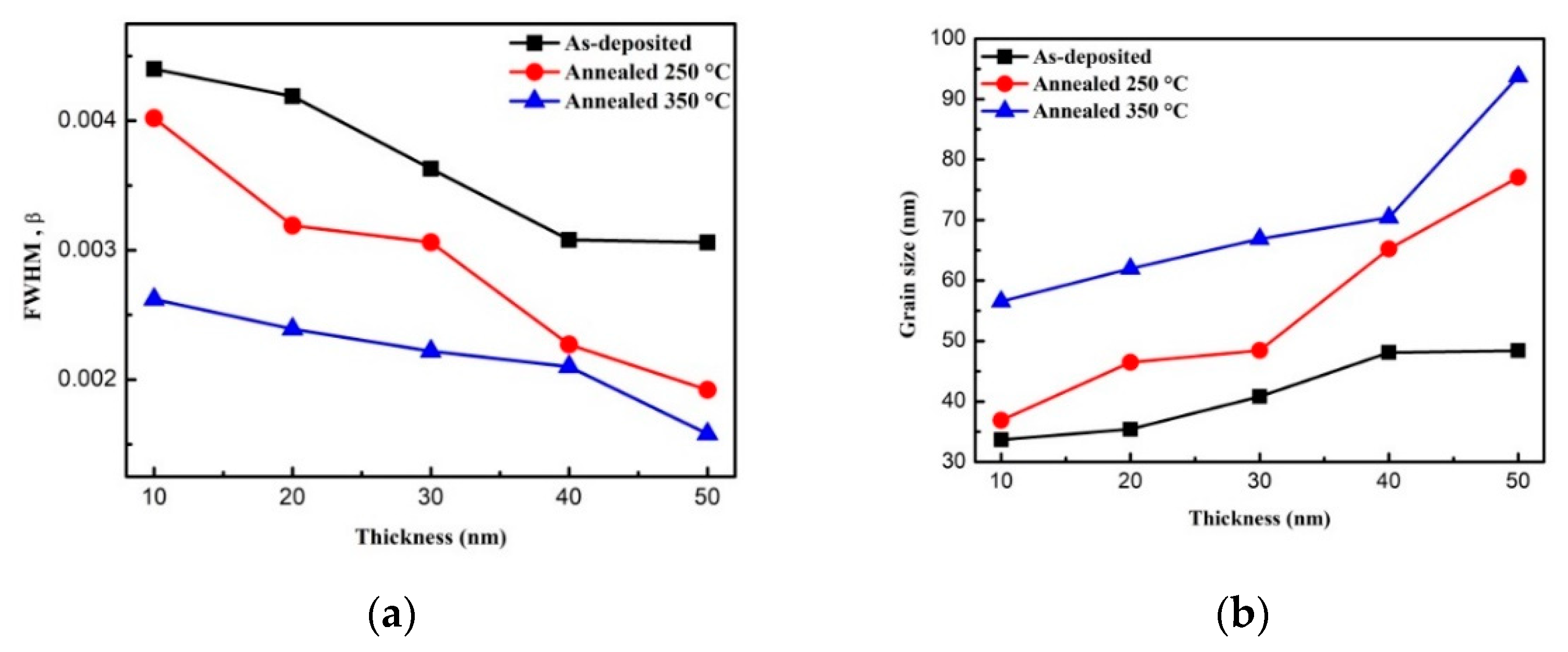
3.1. Full-Width at Half Maximum (FWHM) and Grain Size Distribution
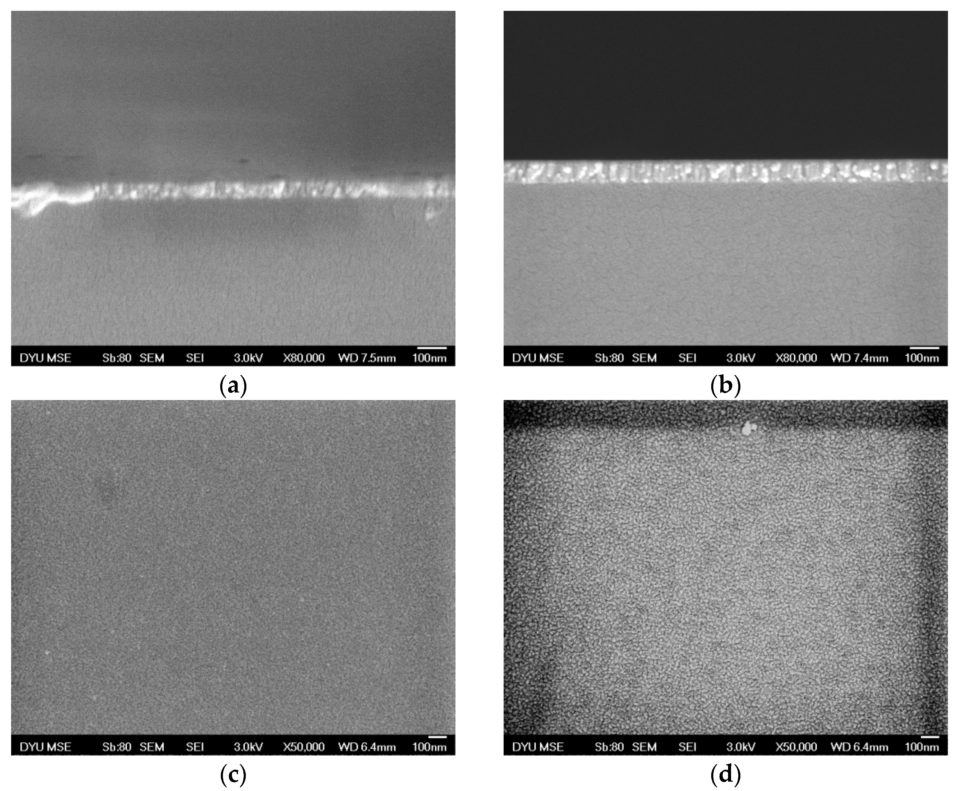
3.2. SEM Image
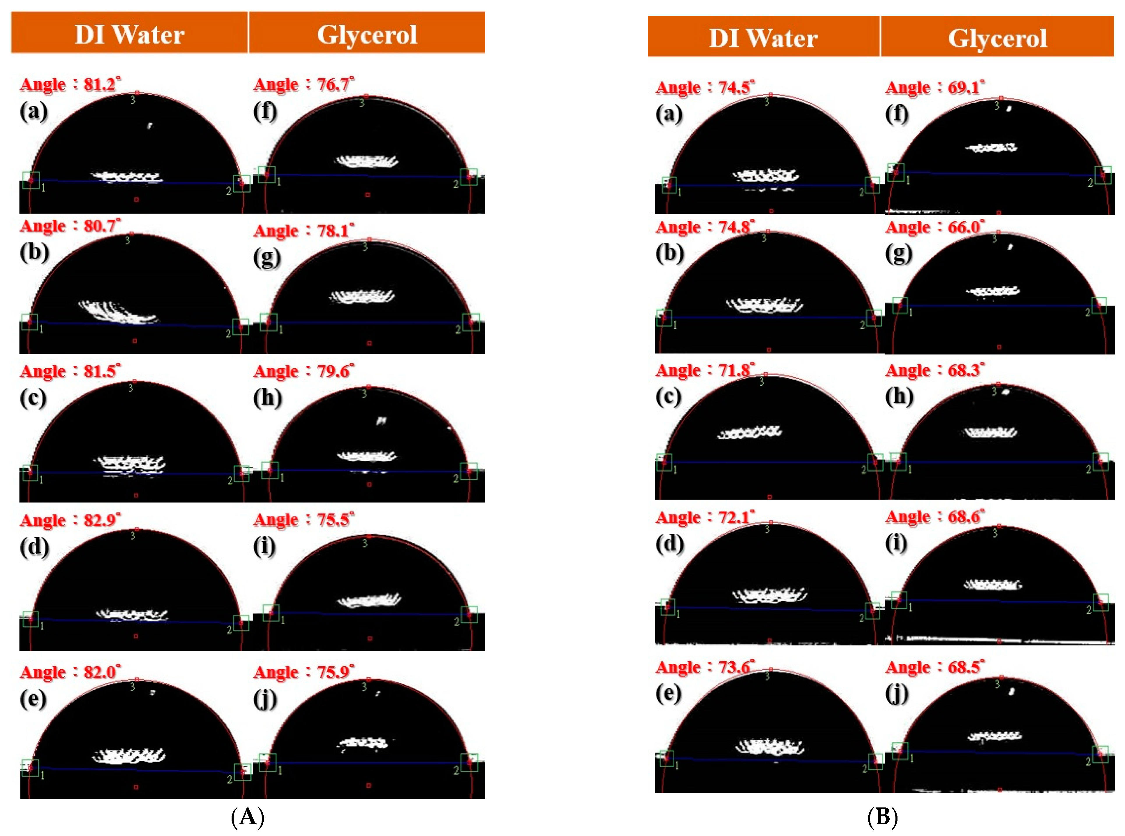
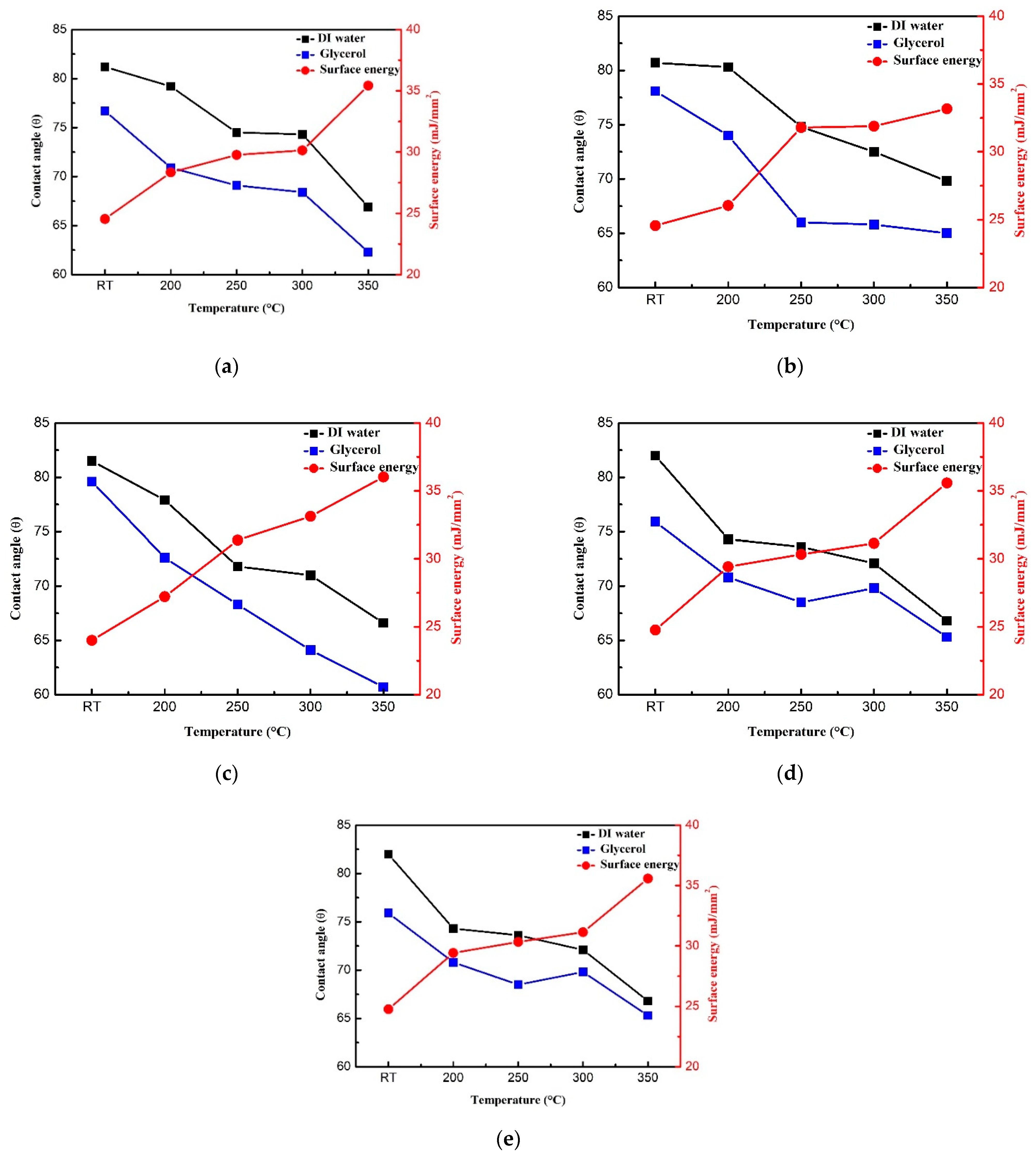
3.3. Contact Angle
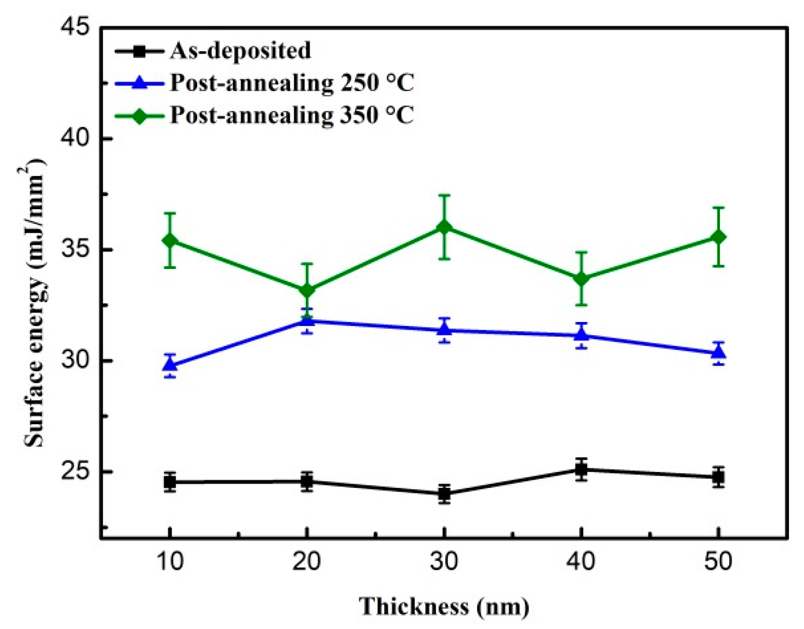
3.4. Surface Energy
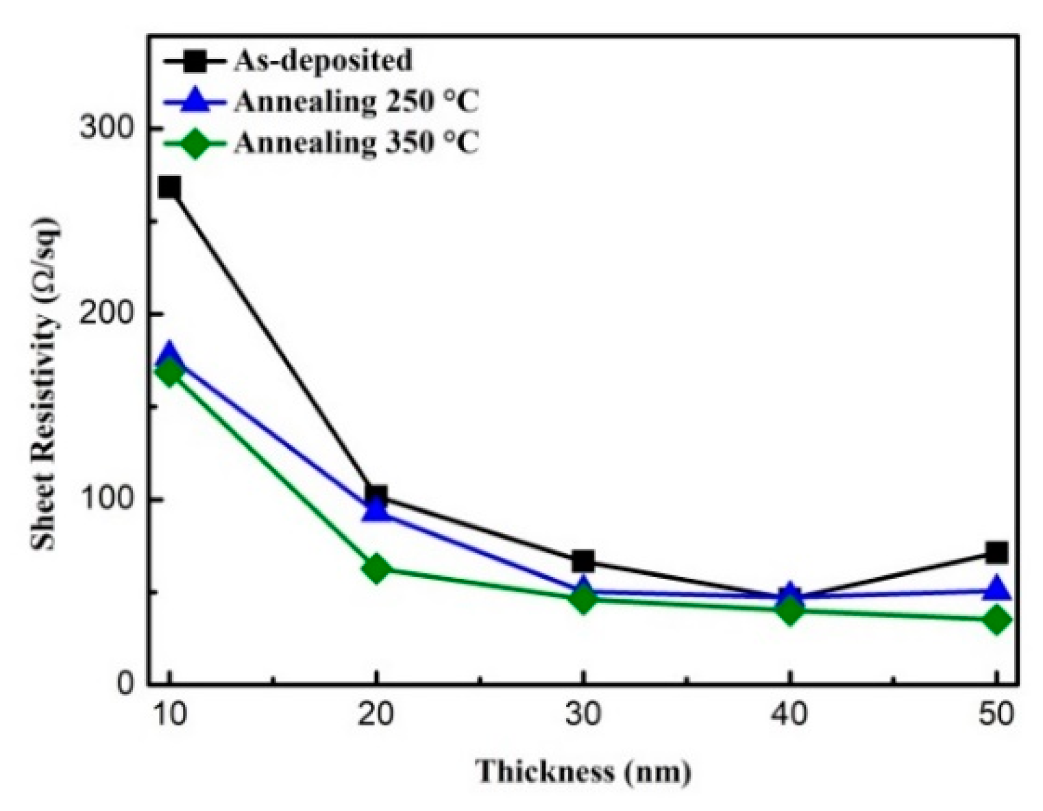
3.5. Electric Property
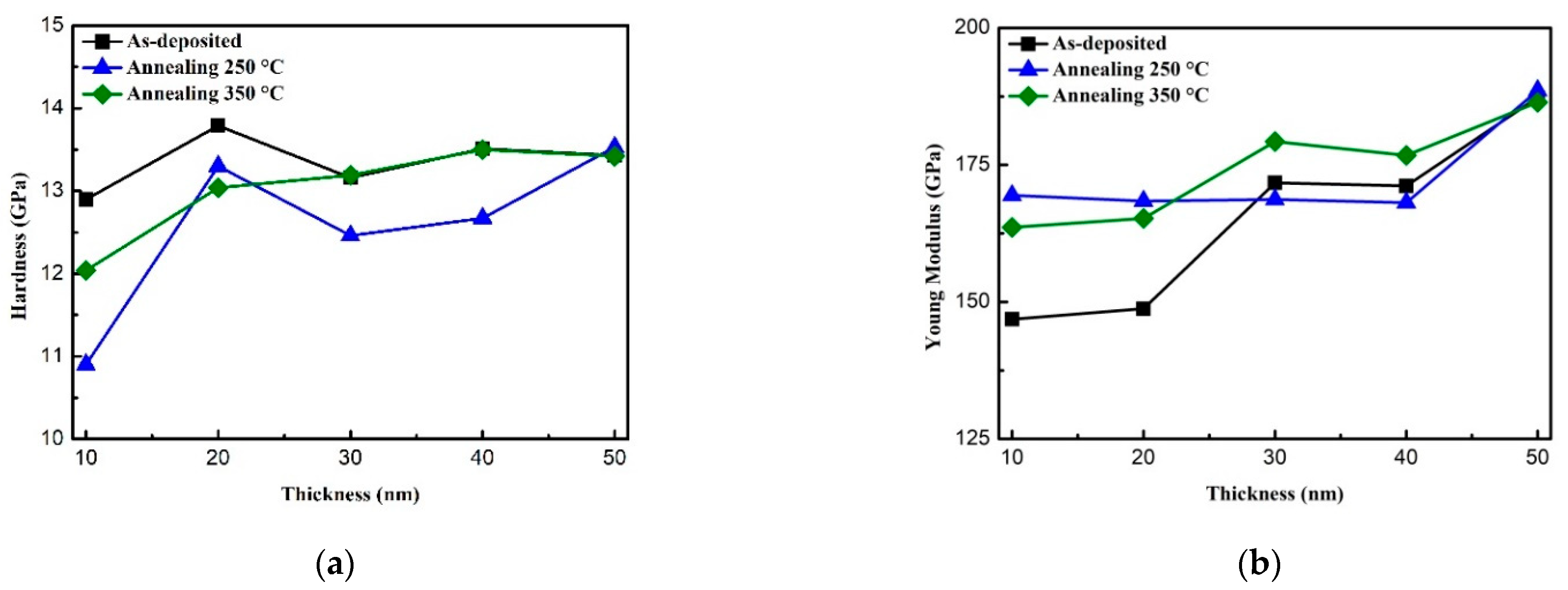
3.6. Nano-Indentation
4. Conclusions
Author Contributions
Funding
Institutional Review Board Statement
Informed Consent Statement
Data Availability Statement
Acknowledgments
Conflicts of Interest
References
- Li, M.; Wang, S.; Zhang, S.; Fang, S.; Feng, G.; Cao, X.; Zhang, P.; Wang, B.; Yu, G. The effect of interfacial oxygen migration on the PMA and thermal stability in MTJ with double MgO layers. Appl. Surf. Sci. 2019, 488, 30–35. [Google Scholar] [CrossRef]
- Iihama, S.; Mizukami, S.; Naganuma, H.; Oogane, M.; Ando, Y.; Miyazaki, T. Gilbert damping constants of Ta/CoFeB/MgO(Ta) thin films measured by optical detection of precessional magnetization dynamics. Phys. Rev. B 2014, 89, 174416. [Google Scholar] [CrossRef]
- Ikeda, S.; Miura, K.; Yamamoto, H.; Mizunuma, K.; Gan, H.D.; Endo, M.; Kanai, S.; Hayakawa, J.; Matsukura, F.; Ohno, H. A perpendicular-anisotropy CoFeB-MgO magnetic tunnel junction. Nat. Mater. 2010, 9, 721–724. [Google Scholar] [CrossRef]
- Wang, S.; Li, M.; Zhang, S.; Fang, S.; Wang, D.; Yu, G. High annealing tolerance and the microstructure study in perpendicular magnetized MgO/CoFeB/MgO structures with thin W spacer layer. J. Magn. Magn. Mater. 2019, 479, 121–125. [Google Scholar] [CrossRef]
- Wolf, S.A.; Awschalom, D.D.; Buhrman, R.A.; Daughton, J.M.; Molnar, S.V.; Roukes, M.L.; Chtchelkanova, A.Y.; Treger, D.M. Spintronics: A spin-based electronics vision for the future. Science 2001, 294, 1488–1495. [Google Scholar] [CrossRef] [Green Version]
- Ikeda, S.; Hayakawa, J.; Ashizawa, Y.; Lee, Y.M.; Miura, K.; Hasegawa, H.; Tsunoda, M.; Matsukura, F.; Ohno, H. Tunnel magnetoresistance of 604% at 300K by suppression of Ta diffusion in CoFeB/MgO/CoFeB pseudo-spin-valves annealed at high temperature. Appl. Phys. Lett. 2008, 93, 082508. [Google Scholar] [CrossRef]
- Parkin, S.S.P.; Kaiser, C.; Panchula, A.; Rice, P.M.; Hughes, B.; Samant, M.; Yang, S.H. Giant tunnelling magnetoresistance at room temperature with MgO (100) tunnel barriers. Nat. Mater. 2004, 3, 862–867. [Google Scholar] [CrossRef] [PubMed]
- Kiselev, S.I.; Sankey, J.C.; Krivorotov, I.N.; Emley, N.C.; Schoelkopf, R.J.; Buhrman, R.A.; Ralph, D.C. Microwave oscillations of a nanomagnet driven by a spin-polarized current. Nature 2003, 425, 380–383. [Google Scholar] [CrossRef] [Green Version]
- Parkin, S.S.P.; Hayashi, M.; Thomas, L. Magnetic domain-wall racetrack memory. Science 2008, 320, 190–194. [Google Scholar] [CrossRef] [PubMed]
- Liu, W.J.; Chang, Y.H.; Chen, Y.T.; Chiang, Y.C.; Tsai, D.Y.; Wu, T.H.; Chi, P.W. Effect of annealing on the characteristics of CoFeBY thin films. Coatings 2021, 11, 250. [Google Scholar] [CrossRef]
- Li, M.; Shi, H.; Yu, G.; Lu, J.; Chen, X.; Han, G.; Yu, G.; Amiri, P.K.; Wang, K.L. Effects of annealing on the magnetic properties and microstructures of Ta/Mo/CoFeB/MgO/Ta films. J. Alloys Compd. 2017, 692, 243–248. [Google Scholar] [CrossRef] [Green Version]
- Almasi, H.; Hickey, D.R.; Newhouse-Illige, T.; Xu, M.; Rosales, M.R.; Nahar, S.; Held, J.T.; Mkhoyan, K.A.; Wang, W.G. Enhanced tunneling magnetoresistance and perpendicular magnetic anisotropy in Mo/CoFeB/MgO magnetic tunnel junctions. Appl. Phys. Lett. 2015, 106, 182406. [Google Scholar] [CrossRef]
- Huang, S.X.; Chen, T.Y.; Chien, C.L. Spin polarization of amorphous CoFeB determined by point-contact Andreev reflection. Appl. Phys. Lett. 2008, 92, 242509. [Google Scholar] [CrossRef]
- Paluskar, P.V.; Attema, J.J.; de Wijs, G.A.; Fiddy, S.; Snoeck, E.; Kohlhepp, J.T.; Swagten, H.J.M.; de Groot, R.A.; Koopmans, B. Spin tunneling in junctions with disordered ferromagnets. Phys. Rev. Lett. 2008, 100, 057205. [Google Scholar] [CrossRef] [Green Version]
- Li, M.; Wang, S.; Zhang, S.; Fang, S.; Yu, G. The perpendicular magnetic anisotropies of CoFeB/MgO films with Nb buffer layers. J. Magn. Magn. Mater. 2019, 485, 187–192. [Google Scholar] [CrossRef]
- Meng, H.; Lum, W.H.; Sbiaa, R.; Lua, S.Y.H.; Tan, H.K. Annealing effects on CoFeB-MgO magnetic tunnel junctions with perpendicular anisotropy. J. Appl. Phys. 2011, 110, 033904. [Google Scholar] [CrossRef]
- Liu, T.; Cai, J.W.; Sun, L. Large enhanced perpendicular magnetic anisotropy in CoFeB/MgO system with the typical Ta buffer replaced by an Hf layer. AIP Adv. 2012, 2, 032151. [Google Scholar] [CrossRef] [Green Version]
- Gottwald, M.; Kan, J.J.; Lee, K.; Zhu, X.; Park, C.; Kang, S.H. Scalable and thermally robust perpendicular magnetic tunnel junctions for STT-MRAM. Appl. Phys. Lett. 2015, 106, 032413. [Google Scholar] [CrossRef]
- Cuchet, L.; Rodmacq, B.; Auffret, S.; Sousa, R.C.; Prejbeanu, I.L.; Dieny, B. Perpendicular magnetic tunnel junctions with a synthetic storage or reference layer: A new route towards Pt- and Pd-free junctions. Sci. Rep. 2016, 6, 21246. [Google Scholar] [CrossRef] [Green Version]
- Kaidatzis, A.; Bran, C.; Psycharis, V.; Vázquez, M.; Martín, J.M.G.; Niarchos, D. Tailoring the magnetic anisotropy of CoFeB/MgO stacks onto W with a Ta buffer layer. Appl. Phys. Lett. 2015, 106, 262401. [Google Scholar] [CrossRef]
- Ghaferi, Z.; Sharafi, S.; Bahrololoom, M.E. The role of electrolyte pH on phase evolution and magnetic properties of CoFeW codeposited films. Appl. Surf. Sci. 2016, 375, 35–41. [Google Scholar] [CrossRef]
- Liu, W.J.; Chang, Y.H.; Chen, Y.T.; Jhou, T.Y.; Chen, Y.H.; Wu, T.H.; Chi, P.W. Impact of annealing on the magnetic and structural of Co40Fe40W20 thin films on Si(100) substrate. Materials 2021, 14, 3017. [Google Scholar] [CrossRef] [PubMed]
- Cullity, B.D. Elements of X-ray Diffraction, 2nd ed.; Addison-Wesley: Reading, MA, USA, 1978. [Google Scholar]
- Patterson, A.L. The Scherrer formula for X-Ray particle size determination. Phys. Rev. 1939, 56, 978–982. [Google Scholar] [CrossRef]
- Kitamura, M.; Kuzumoto, Y.; Kamura, M.; Aomori, S.; Na, J.H.; Arakawa, Y. Low-voltage-operating fullerene C60 thin-film transistors with various surface treatments. Phys. Stat. Solidi C 2008, 5, 3181–3183. [Google Scholar] [CrossRef]
- Beaini, S.S.; Kronawitter, C.X.; Carey, V.P.; Mao, S.S. ZnO deposition on metal substrates: Relating fabrication, morphology and wettability. J. Appl. Phys. 2013, 113, 184905. [Google Scholar] [CrossRef]
- Yao, G.; Zhang, M.; Lv, J.; Xu, K.; Shi, S.; Gong, Z.; Tao, J.; Jiang, X.; Yang, L.; Cheng, Y.; et al. Effects of electrodeposition electrolyte concentration on microstructure, optical properties and wettability of ZnO nanorods. J. Electrochem. Soc. 2015, 162, D300–D304. [Google Scholar] [CrossRef]
- Dhaygude, H.D.; Shinde, S.K.; Velhal, N.B.; Takale, M.V.; Fulari, V.J. Doping effect on SILAR synthesized crystalline nanostructured Cudoped ZnO thin films grown on indium tin oxide (ITO) coated glass substrates and its characterization. Mater. Res. Express 2016, 3, 086402. [Google Scholar] [CrossRef]
- Owens, D.K.; Wendt, R.C. Estimation of the surface free energy of polymers. J. Appl. Polym. Sci. 1969, 13, 1741–1747. [Google Scholar] [CrossRef]
- Kaelble, D.H.; Uy, K.C. A Reinterpretation of organic liquid-polytetrafluoroethylene surface interactions. J. Adhens. 1970, 2, 50–60. [Google Scholar] [CrossRef]
- Liu, W.J.; Chang, Y.H.; Chen, Y.T.; Chiang, Y.C.; Liu, Y.C.; Wu, T.H.; Chi, P.W. Effect of annealing on the structural, magnetic and surface energy of CoFeBY films on Si(100) substrate. Materials 2021, 14, 987. [Google Scholar] [CrossRef]
- Pachchigar, V.; Ranjan, M.; Mukherjee, S. Role of hierarchical protrusions in water repellent superhydrophobic PTFE surface produced by low energy ion beam irradiation. Sci. Rep. 2019, 9, 8675. [Google Scholar] [CrossRef] [Green Version]
- Liu, W.J.; Chang, Y.H.; Ou, S.L.; Chen, Y.T.; Liang, Y.C.; Huang, B.J.; Chu, C.L.; Chiang, C.C.; Wu, T.H. Magnetic properties, adhesion, and nanomechanical property of Co40Fe40W20 films on Si (100) substrate. J. Nanomater. 2020, 2020, 1584310. [Google Scholar] [CrossRef]
- Liu, W.J.; Chang, Y.H.; Ou, S.L.; Chen, Y.T.; Li, W.H.; Jhou, T.Y.; Chu, C.L.; Wu, T.H.; Tseng, S.W. Effect of annealing on the structural, magnetic, surface energy and optical properties of Co32Fe30W38 films deposited by direct-current magnetron sputtering. Coatings 2020, 10, 1028. [Google Scholar] [CrossRef]
- Jassim, S.A.J.; Zumaila, A.A.R.A.; Waly, G.A.A.A. Influence of substrate temperature on the structural, optical and electrical properties of CdS thin films deposited by thermal evaporation. Res. Phys. 2013, 3, 173–178. [Google Scholar] [CrossRef] [Green Version]
- Redjdal, N.; Salah, H.; Hauet, T.; Menari, H.; Chérif, S.M.; Gabouze, N.; Azzaz, M. Microstructural electrical and magnetic properties of Fe35Co65 thin films grown by thermal evaporation from mechanically alloyed powders. Thin Solid Films 2014, 552, 164–169. [Google Scholar] [CrossRef] [Green Version]
- Oliver, W.C.; Pharr, G.M. An improved technique for determining hardness and elastic modulus using load and displacement sensing indentation experiments. J. Mater. Res. 1992, 7, 1564–1583. [Google Scholar] [CrossRef]
- Zhu, J.; Han, J.; Liu, A.; Meng, S.; Jiang, C. Mechanical properties and Raman characterization of amorphous diamond films as a function of film thickness. Surf. Coat. Technol. 2007, 201, 6667–6669. [Google Scholar] [CrossRef]


| Process | Thickness | Contact Angle with DI Water (θ) | Contact Angle with Glycerol (θ) | Surface Energy (mJ/mm2) | Grain Size (nm) |
|---|---|---|---|---|---|
| As-deposited | 10 nm | 81.2° | 76.7° | 24.55 | 33.6 |
| 20 nm | 80.7° | 78.1° | 24.56 | 35.4 | |
| 30 nm | 81.5° | 79.6° | 24.00 | 40.8 | |
| 40 nm | 82.9° | 75.5° | 25.10 | 48.1 | |
| 50 nm | 82.0° | 75.9° | 24.76 | 48.4 | |
| Post-annealing 250 °C | 10 nm | 74.5° | 69.1° | 29.77 | 36.8 |
| 20 nm | 74.8° | 66.0° | 31.79 | 46.5 | |
| 30 nm | 71.8° | 68.3° | 31.37 | 48.4 | |
| 40 nm | 72.1° | 68.6° | 31.13 | 65.2 | |
| 50 nm | 73.6° | 68.5° | 30.33 | 77.1 | |
| Post-annealing 350 °C | 10 nm | 66.9° | 62.3° | 35.42 | 56.5 |
| 20 nm | 69.8° | 65.0° | 33.17 | 61.9 | |
| 30 nm | 66.6° | 60.7° | 36.02 | 66.9 | |
| 40 nm | 69.1° | 67.6° | 33.69 | 70.4 | |
| 50 nm | 66.8° | 65.3° | 35.58 | 93.7 |
| Material | Surface Energy (mJ/mm2) | Factor |
|---|---|---|
| Si(100)/Co40Fe40W20 (✽Current research) | 24.00–36.02 | Because thin films have largest grain size, there is highest surface energy. |
| Glass/CoFeBY [10] | 23.89–31.07 | The crystallinity of samples was weak. |
| Si(100)/CoFeBY [31] | 24.55–31.85 | The crystallinity of samples was weak. |
| Si(100)/Co40Fe40W20 [33] | 23.61–30.12 | At 42 nm, because the crystal of thin films have highest surface energy in paper. |
| Glass/Co32Fe30W38 [34] | 22.3–28.6 | Crystallinity: Si(100) > glass therefore, the surface energy of Glass/Co32Fe30W38 is lower. |
Publisher’s Note: MDPI stays neutral with regard to jurisdictional claims in published maps and institutional affiliations. |
© 2021 by the authors. Licensee MDPI, Basel, Switzerland. This article is an open access article distributed under the terms and conditions of the Creative Commons Attribution (CC BY) license (https://creativecommons.org/licenses/by/4.0/).
Share and Cite
Liu, W.-J.; Chang, Y.-H.; Fern, C.-L.; Chen, Y.-T.; Jhou, T.-Y.; Chiu, P.-C.; Lin, S.-H.; Lin, K.-W.; Wu, T.-H. Annealing Effect on the Contact Angle, Surface Energy, Electric Property, and Nanomechanical Characteristics of Co40Fe40W20 Thin Films. Coatings 2021, 11, 1268. https://doi.org/10.3390/coatings11111268
Liu W-J, Chang Y-H, Fern C-L, Chen Y-T, Jhou T-Y, Chiu P-C, Lin S-H, Lin K-W, Wu T-H. Annealing Effect on the Contact Angle, Surface Energy, Electric Property, and Nanomechanical Characteristics of Co40Fe40W20 Thin Films. Coatings. 2021; 11(11):1268. https://doi.org/10.3390/coatings11111268
Chicago/Turabian StyleLiu, Wen-Jen, Yung-Huang Chang, Chi-Lon Fern, Yuan-Tsung Chen, Tian-Yi Jhou, Po-Chun Chiu, Shih-Hung Lin, Ko-Wei Lin, and Te-Ho Wu. 2021. "Annealing Effect on the Contact Angle, Surface Energy, Electric Property, and Nanomechanical Characteristics of Co40Fe40W20 Thin Films" Coatings 11, no. 11: 1268. https://doi.org/10.3390/coatings11111268