Two-Dimensional Transition Metal Dichalcogenide Based Biosensors: From Fundamentals to Healthcare Applications


Abstract
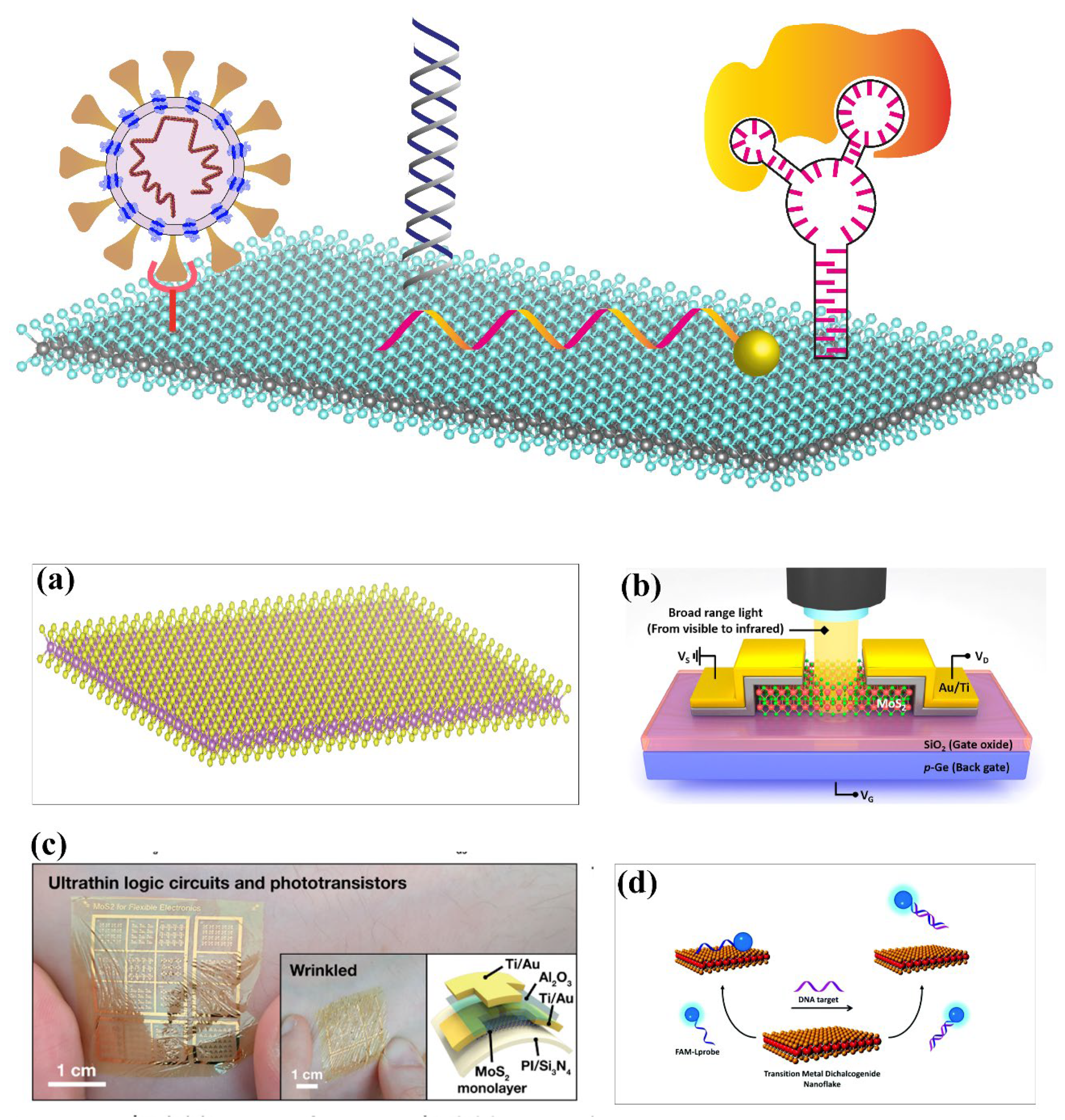
:1. Introduction
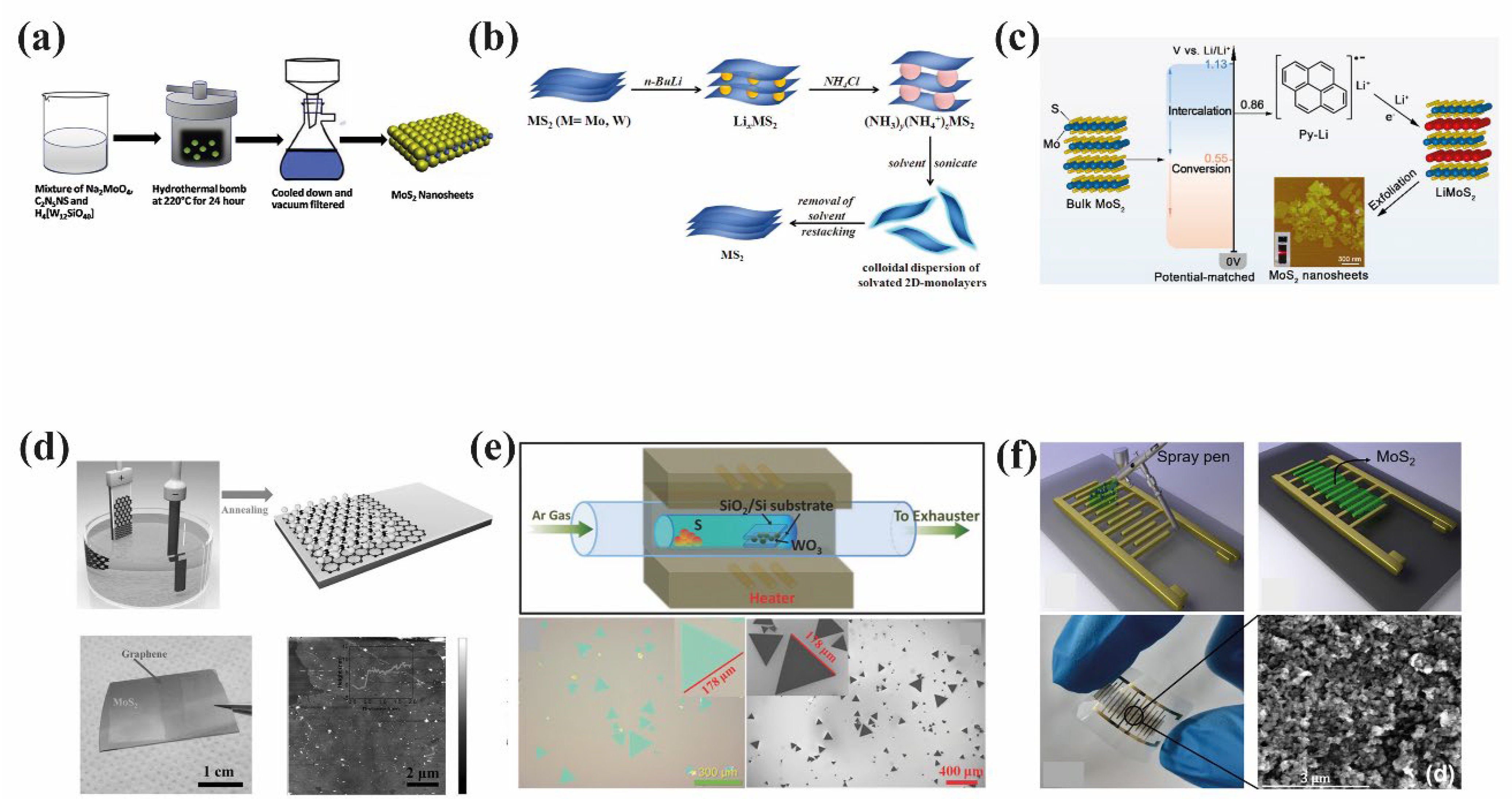
2. Synthesis of 2D TMD Materials
3. Biosensing Using 2D TMD Materials
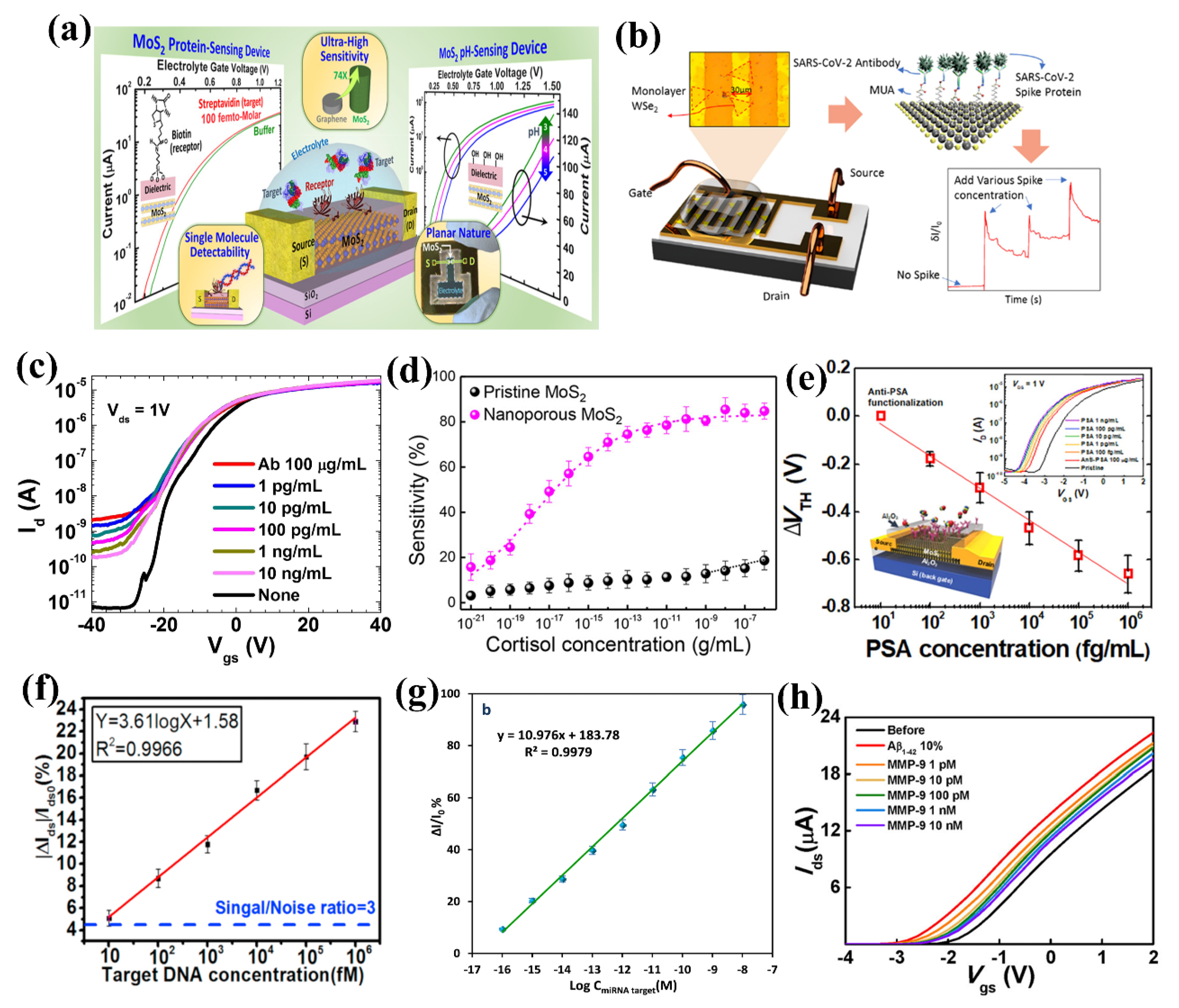
3.1. Electrical Biosensors
3.1.1. Biomarker Detection

3.1.2. Detection of Bacteria and Virus
3.1.3. Detection of DNAs

| Matrix | Method | Target Analyte | Linear Range | LoD | Reference |
|---|---|---|---|---|---|
| Multi-layer MoS2 | FET based | PSA | 375 fM | [79] | |
| Multi-layer MoS2 | FET based | PSA | 1 pg/mL–10 ng/mL | 1 pg/mL | [57] |
| Multi-layer MoS2 | FET based | PSA | 1 pg/mL–1 ng/mL | 1 pg/mL | [119] |
| Multi-layer MoS2 | FET based | PSA | 100 fg/mL–1 ng/mL | 100 fg/mL | [116] |
| Multi-layer WSe2 | FET based | PSA | 10 fg/mL–1 ng/mL | 10 fg/mL | [60] |
| Multi-layer MoS2 | FET based | miRNA-155 | 0.1 fM–10 nM | 0.03 fM | [56] |
| Multi-layer MoS2 | FET based | Circulating protein | 1 pM–10 nM | 1 pM | [117] |
| Multi-layer MoS2 | FET based | cortisol | 1 ag/mL–1 µm/mL | 1 ag/mL | [70] |
| MoS2/TiO2 | FET based | S. Aurus | 50–106 cfu/mL | 50 cfu/mL | [128] |
| Monolayer WSe2 | FET based | SARS-CoV-2 | 25 fg/µL–10 ng/µL | 25 fg/µL | [115] |
| Multi-layer MoS2 | FET based | DNA | 10 fM–10 nM | 10 fM | [129] |
| Few-layer MoS2 | FET based | DNA | 10 fM–1 nM | 6 fM | [29] |
| Monolayer MoS2 | FET based | DNA | 100 aM–100 fM | 100 aM | [36] |
| Monolayer WS2 | FET based | DNA | 0.1 fM–1 nM | 3 aM | [130] |
| Multi-layer MoS2 | FET based | Streptavidin | 100 fM | [59] | |
| Multi-layer MoS2 | FET based | TNF-α | 60 fM–6 pM | 60 fM | [131] |
| Multi-layer MoS2 and WSe2 | FET based | TNF-α and Streptavidin | 60 fM–6 pM and 70 fM–70 pM | 60 fM and 70 fM | [132] |
| Monolayer-bilayer | FET based | kanamycin | 1 nM–100 µM | 0.66 nM | [133] |
| MoS2/rGO | FET based | H2O2 | 1 pM–100 nM | 1 pM | [134] |
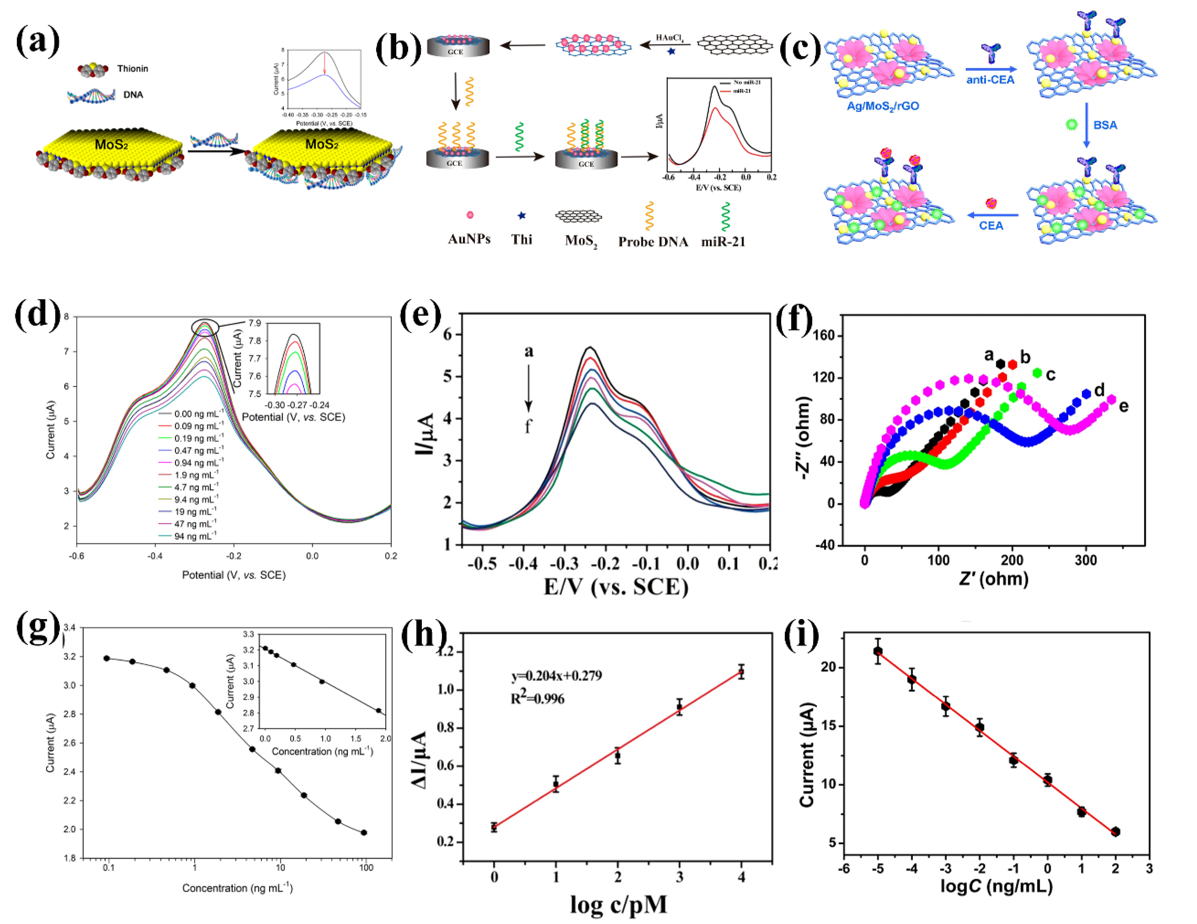
3.2. Electrochemical Biosensors
3.2.1. Detection of Biomarkers
3.2.2. Detection of Bacteria and Virus
3.2.3. Detection of DNAs and Other Bio-Analytes
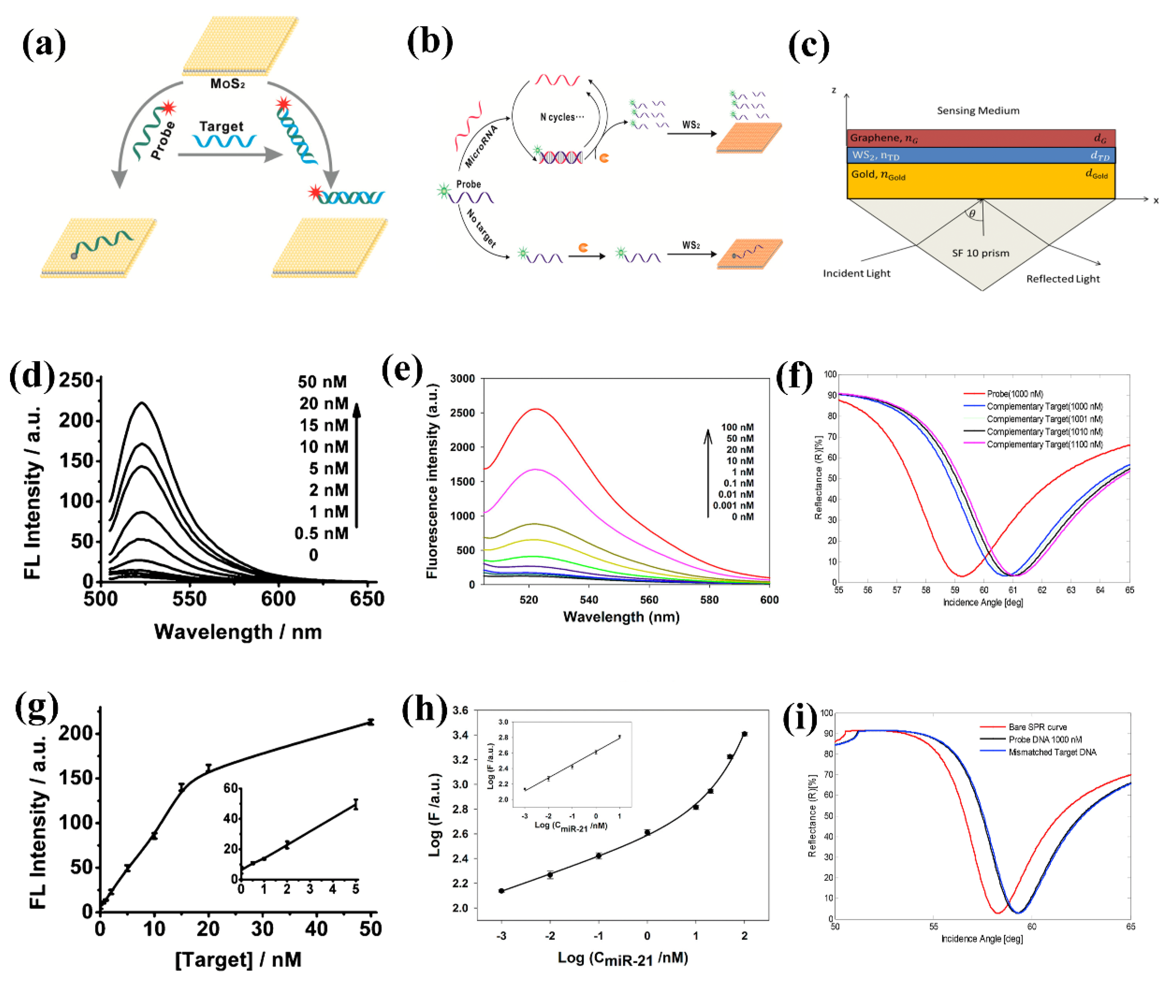
3.3. Optical Biosensors
3.3.1. Biomarker Detection
3.3.2. Detection of Bacteria and Virus
3.3.3. Detection of DNAs and Other Biomolecules
4. Future Perspectives
Author Contributions
Funding
Institutional Review Board Statement
Informed Consent Statement
Data Availability Statement
Conflicts of Interest
References
- Novoselov, K.S.; Geim, A.K.; Morozov, S.V.; Jiang, D.; Zhang, Y.; Dubonos, S.V.; Grigorieva, I.V.; Firsov, A.A. Electric Field Effect in Atomically Thin Carbon Films. Science 2004, 306, 666–669. [Google Scholar] [CrossRef] [PubMed] [Green Version]
- Bolotin, K.I.; Sikes, K.J.; Jiang, Z.; Klima, M.; Fudenberg, G.; Hone, J.; Kim, P.; Stormer, H.L. Ultrahigh Electron Mobility in Suspended Graphene. Solid State Commun. 2008, 146, 351–355. [Google Scholar] [CrossRef] [Green Version]
- Xia, F.; Mueller, T.; Lin, Y.; Valdes-Garcia, A.; Avouris, P. Ultrafast Graphene Photodetector. Nat. Nanotechol. 2009, 4, 839–843. [Google Scholar] [CrossRef] [PubMed] [Green Version]
- Lin, Y.-M.; Jenkins, K.A.; Valdes-Garcia, A.; Small, J.P.; Farmer, D.B.; Avouris, P. Operation of Graphene Transistors at Gigahertz Frequencies. Nano Lett. 2009, 9, 422–426. [Google Scholar] [CrossRef] [PubMed] [Green Version]
- Mittendorff, M.; Winnerl, S.; Kamann, J.; Eroms, J.; Weiss, D.; Schneider, H.; Helm, M. Ultrafast Graphene-Based Broadband THz Detector. Appl. Phys. Lett. 2013, 103, 021113. [Google Scholar] [CrossRef]
- Mueller, T.; Xia, F.; Avouris, P. Graphene Photodetectors for High-Speed Optical Communications. Nat. Photon. 2010, 4, 297–301. [Google Scholar] [CrossRef] [Green Version]
- Zhang, B.Y.; Liu, T.; Meng, B.; Li, X.; Liang, G.; Hu, X.; Wang, Q.J. Broadband High Photoresponse from Pure Monolayer Graphene Photodetector. Nat. Commun. 2013, 4, 1811. [Google Scholar] [CrossRef] [Green Version]
- Yoon, H.J.; Jun, D.H.; Yang, J.H.; Zhou, Z.; Yang, S.S.; Cheng, M.M.-C. Carbon Dioxide Gas Sensor Using a Graphene Sheet. Sens. Actuators B Chem. 2011, 157, 310–313. [Google Scholar] [CrossRef]
- Tian, W.; Liu, X.; Yu, W. Research Progress of Gas Sensor Based on Graphene and Its Derivatives: A Review. Appl. Sci. 2018, 8, 1118. [Google Scholar] [CrossRef] [Green Version]
- Justino, C.I.L.; Gomes, A.R.; Freitas, A.C.; Duarte, A.C.; Rocha-Santos, T.A.P. Graphene Based Sensors and Biosensors. TrAC Trends Anal. Chem. 2017, 91, 53–66. [Google Scholar] [CrossRef]
- De, S.; Coleman, J.N. Are There Fundamental Limitations on the Sheet Resistance and Transmittance of Thin Graphene Films? ACS Nano 2010, 4, 2713–2720. [Google Scholar] [CrossRef]
- Novoselov, K.S.; Geim, A.K.; Morozov, S.V.; Jiang, D.; Katsnelson, M.I.; Grigorieva, I.V.; Dubonos, S.V.; Firsov, A.A. Two-Dimensional Gas of Massless Dirac Fermions in Graphene. Nature 2005, 438, 197–200. [Google Scholar] [CrossRef] [Green Version]
- Lee, S.Y.; Duong, D.L.; Vu, Q.A.; Jin, Y.; Kim, P.; Lee, Y.H. Chemically Modulated Band Gap in Bilayer Graphene Memory Transistors with High On/Off Ratio. ACS Nano 2015, 9, 9034–9042. [Google Scholar] [CrossRef]
- Xiao, S.; Chen, J.-H.; Adam, S.; Williams, E.D.; Fuhrer, M.S. Charged Impurity Scattering in Bilayer Graphene. Phys. Rev. B 2010, 82, 041406. [Google Scholar] [CrossRef] [Green Version]
- Huu, H.T.; Thi, X.D.N.; Van, K.N.; Kim, S.J.; Vo, V. A Facile Synthesis of MoS2/g-C3N4 Composite as an Anode Material with Improved Lithium Storage Capacity. Materials 2019, 12, 1730. [Google Scholar] [CrossRef] [Green Version]
- Ping, J.; Fan, Z.; Sindoro, M.; Ying, Y.; Zhang, H. Recent Advances in Sensing Applications of Two-Dimensional Transition Metal Dichalcogenide Nanosheets and Their Composites. Adv. Funct. Mater. 2017, 27, 1605817. [Google Scholar] [CrossRef]
- Molaei, M.J. Two-Dimensional (2D) Materials beyond Graphene in Cancer Drug Delivery, Photothermal and Photodynamic Therapy, Recent Advances and Challenges Ahead: A Review. J. Drug Deliv. Sci. Technol. 2021, 61, 101830. [Google Scholar] [CrossRef]
- Bolotsky, A.; Butler, D.; Dong, C.; Gerace, K.; Glavin, N.R.; Muratore, C.; Robinson, J.A.; Ebrahimi, A. Two-Dimensional Materials in Biosensing and Healthcare: From In Vitro Diagnostics to Optogenetics and Beyond. ACS Nano 2019, 13, 9781–9810. [Google Scholar] [CrossRef] [Green Version]
- Sinha, A.; Dhanjai; Zhao, H.; Huang, Y.; Lu, X.; Chen, J.; Jain, R. MXene: An Emerging Material for Sensing and Biosensing. TrAC Trends Anal. Chem. 2018, 105, 424–435. [Google Scholar] [CrossRef]
- Ménard-Moyon, C.; Bianco, A.; Kalantar-Zadeh, K. Two-Dimensional Material-Based Biosensors for Virus Detection. ACS Sens. 2020, 5, 3739–3769. [Google Scholar] [CrossRef]
- Garg, M.; Gupta, A.; Sharma, A.L.; Singh, S. Advancements in 2D Materials Based Biosensors for Oxidative Stress Biomarkers. ACS Appl. Bio Mater. 2021, 4, 5944–5960. [Google Scholar] [CrossRef] [PubMed]
- Zheng, W.; Jiang, Y.; Hu, X.; Li, H.; Zeng, Z.; Wang, X.; Pan, A. Light Emission Properties of 2D Transition Metal Dichalcogenides: Fundamentals and Applications. Adv. Opt. Mater. 2018, 6, 1800420. [Google Scholar] [CrossRef]
- Choi, W.; Choudhary, N.; Han, G.H.; Park, J.; Akinwande, D.; Lee, Y.H. Recent Development of Two-Dimensional Transition Metal Dichalcogenides and Their Applications. Mater. Today 2017, 20, 116–130. [Google Scholar] [CrossRef]
- Lv, R.; Robinson, J.A.; Schaak, R.E.; Sun, D.; Sun, Y.; Mallouk, T.E.; Terrones, M. Transition Metal Dichalcogenides and Beyond: Synthesis, Properties, and Applications of Single- and Few-Layer Nanosheets. Acc. Chem. Res. 2015, 48, 56–64. [Google Scholar] [CrossRef] [PubMed]
- Sebastian, A.; Pendurthi, R.; Choudhury, T.H.; Redwing, J.M.; Das, S. Benchmarking Monolayer MoS2 and WS2 Field-Effect Transistors. Nat. Commun. 2021, 12, 693. [Google Scholar] [CrossRef]
- Das, S.; Sebastian, A.; Pop, E.; McClellan, C.J.; Franklin, A.D.; Grasser, T.; Knobloch, T.; Illarionov, Y.; Penumatcha, A.V.; Appenzeller, J.; et al. Transistors Based on Two-Dimensional Materials for Future Integrated Circuits. Nat. Electron. 2021, 4, 786–799. [Google Scholar] [CrossRef]
- Mawlong, L.P.; Paul, K.K.; Giri, P.K. Simultaneous Photoluminescence Enhancement in CVD Grown Single Layer MoS2 and TiO2 NRs in the MoS2@TiO2 Heterojunction. In Proceedings of the AIP Conference Proceedings, Kerala, India, 3–5 January 2019; AIP Publishing LLC: Melville, NY, USA, 2019; Volume 2082, p. 040004. [Google Scholar]
- Zhu, B.; Chen, X.; Cui, X. Exciton Binding Energy of Monolayer WS2. Sci. Rep. 2015, 5, 9218. [Google Scholar] [CrossRef] [Green Version]
- Mei, J.; Li, Y.-T.; Zhang, H.; Xiao, M.-M.; Ning, Y.; Zhang, Z.-Y.; Zhang, G.-J. Molybdenum Disulfide Field-Effect Transistor Biosensor for Ultrasensitive Detection of DNA by Employing Morpholino as Probe. Biosens. Bioelectron. 2018, 110, 71–77. [Google Scholar] [CrossRef]
- Chen, J.; Wang, Q.; Sheng, Y.; Cao, G.; Yang, P.; Shan, Y.; Liao, F.; Muhammad, Z.; Bao, W.; Hu, L.; et al. High-Performance WSe2 Photodetector Based on a Laser-Induced p–n Junction. ACS Appl. Mater. Interfaces 2019, 11, 43330–43336. [Google Scholar] [CrossRef]
- Liu, T.; Wang, C.; Gu, X.; Gong, H.; Cheng, L.; Shi, X.; Feng, L.; Sun, B.; Liu, Z. Drug Delivery with PEGylated MoS2 Nano-Sheets for Combined Photothermal and Chemotherapy of Cancer. Adv. Mater. 2014, 26, 3433–3440. [Google Scholar] [CrossRef]
- Li, B.L.; Setyawati, M.I.; Chen, L.; Xie, J.; Ariga, K.; Lim, C.-T.; Garaj, S.; Leong, D.T. Directing Assembly and Disassembly of 2D MoS2 Nanosheets with DNA for Drug Delivery. ACS Appl. Mater. Interfaces 2017, 9, 15286–15296. [Google Scholar] [CrossRef]
- Pumera, M.; Loo, A.H. Layered Transition-Metal Dichalcogenides (MoS2 and WS2) for Sensing and Biosensing. TrAC Trends Anal. Chem. 2014, 61, 49–53. [Google Scholar] [CrossRef]
- Kim, S.-G.; Kim, S.-H.; Park, J.; Kim, G.-S.; Park, J.-H.; Saraswat, K.C.; Kim, J.; Yu, H.-Y. Infrared Detectable MoS2 Phototransistor and Its Application to Artificial Multilevel Optic-Neural Synapse. ACS Nano 2019, 13, 10294–10300. [Google Scholar] [CrossRef]
- Li, X.; Li, X.; Li, Z.; Wang, J.; Zhang, J. WS2 Nanoflakes Based Selective Ammonia Sensors at Room Temperature. Sens. Actuators B Chem. 2017, 240, 273–277. [Google Scholar] [CrossRef]
- Liu, J.; Chen, X.; Wang, Q.; Xiao, M.; Zhong, D.; Sun, W.; Zhang, G.; Zhang, Z. Ultrasensitive Monolayer MoS2 Field-Effect Transistor Based DNA Sensors for Screening of Down Syndrome. Nano Lett. 2019, 19, 1437–1444. [Google Scholar] [CrossRef]
- Gutiérrez, H.R.; Perea-López, N.; Elías, A.L.; Berkdemir, A.; Wang, B.; Lv, R.; López-Urías, F.; Crespi, V.H.; Terrones, H.; Terrones, M. Extraordinary Room-Temperature Photoluminescence in Triangular WS2 Monolayers. Nano Lett. 2013, 13, 3447–3454. [Google Scholar] [CrossRef] [Green Version]
- Kang, M.; Kim, B.; Ryu, S.H.; Jung, S.W.; Kim, J.; Moreschini, L.; Jozwiak, C.; Rotenberg, E.; Bostwick, A.; Kim, K.S. Universal Mechanism of Band-Gap Engineering in Transition-Metal Dichalcogenides. Nano Lett. 2017, 17, 1610–1615. [Google Scholar] [CrossRef] [Green Version]
- Kang, K.; Xie, S.; Huang, L.; Han, Y.; Huang, P.Y.; Mak, K.F.; Kim, C.-J.; Muller, D.; Park, J. High-Mobility Three-Atom-Thick Semiconducting Films with Wafer-Scale Homogeneity. Nature 2015, 520, 656–660. [Google Scholar] [CrossRef]
- Lan, C.; Zhou, Z.; Zhou, Z.; Li, C.; Shu, L.; Shen, L.; Li, D.; Dong, R.; Yip, S.; Ho, J.C. Wafer-Scale Synthesis of Monolayer WS2 for High-Performance Flexible Photodetectors by Enhanced Chemical Vapor Deposition. Nano Res. 2018, 11, 3371–3384. [Google Scholar] [CrossRef]
- Bora, A.; Mawlong, L.P.; Giri, P.K. Highly Suppressed Dark Current and Fast Photoresponse from Au Nanoparticle-Embedded, Si/Au/WS2 Quantum-Dot-Based, Self-Biased Schottky Photodetectors. ACS Appl. Electron. Mater. 2021, 3, 4891–4904. [Google Scholar] [CrossRef]
- Ovchinnikov, D.; Allain, A.; Huang, Y.-S.; Dumcenco, D.; Kis, A. Electrical Transport Properties of Single-Layer WS2. ACS Nano 2014, 8, 8174–8181. [Google Scholar] [CrossRef] [PubMed]
- Huiling Loo, A.; Bonanni, A.; Pumera, M. Strong Dependence of Fluorescence Quenching on the Transition Metal in Layered Transition Metal Dichalcogenide Nanoflakes for Nucleic Acid Detection. Analyst 2016, 141, 4654–4658. [Google Scholar] [CrossRef]
- Kim, J.; Seung, H.; Kang, D.; Kim, J.; Bae, H.; Park, H.; Kang, S.; Choi, C.; Choi, B.K.; Kim, J.S.; et al. Wafer-Scale Production of Transition Metal Dichalcogenides and Alloy Monolayers by Nanocrystal Conversion for Large-Scale Ultrathin Flexible Electronics. Nano Lett. 2021, 21, 9153–9163. [Google Scholar] [CrossRef] [PubMed]
- Pereira, N.M.; Rezende, N.P.; Cunha, T.H.R.; Barboza, A.P.M.; Silva, G.G.; Lippross, D.; Neves, B.R.A.; Chacham, H.; Ferlauto, A.S.; Lacerda, R.G. Aerosol-Printed MoS2 Ink as a High Sensitivity Humidity Sensor. ACS Omega 2022, 7, 9388–9396. [Google Scholar] [CrossRef]
- Jin, K.; Xie, L.; Tian, Y.; Liu, D. Au-Modified Monolayer MoS2 Sensor for DNA Detection. J. Phys. Chem. C 2016, 120, 11204–11209. [Google Scholar] [CrossRef]
- KiKrubasankar, B.; Won, Y.S.; Adofo, L.A.; Choi, S.H.; Kim, S.M.; Kim, K.K. Atomic and Structural Modifications of Two-Dimensional Transition Metal Dichalcogenides for Various Advanced Applications. Chem. Sci. 2022, 13, 7707–7738. [Google Scholar] [CrossRef]
- Nolan, M.; O’Callaghan, S.; Fagas, G.; Greer, J.C.; Frauenheim, T. Silicon Nanowire Band Gap Modification. Nano Lett. 2007, 7, 34–38. [Google Scholar] [CrossRef] [Green Version]
- Xu, M.; Liang, T.; Shi, M.; Chen, H. Graphene-Like Two-Dimensional Materials. Chem. Rev. 2013, 113, 3766–3798. [Google Scholar] [CrossRef]
- Rao, R.; Pint, C.L.; Islam, A.E.; Weatherup, R.S.; Hofmann, S.; Meshot, E.R.; Wu, F.; Zhou, C.; Dee, N.; Amama, P.B.; et al. Carbon Nanotubes and Related Nanomaterials: Critical Advances and Challenges for Synthesis toward Mainstream Commercial Applications. ACS Nano 2018, 12, 11756–11784. [Google Scholar] [CrossRef] [Green Version]
- George, A.S.; Mutlu, Z.; Ionescu, R.; Wu, R.J.; Jeong, J.S.; Bay, H.H.; Chai, Y.; Mkhoyan, K.A.; Ozkan, M.; Ozkan, C.S. Wafer Scale Synthesis and High Resolution Structural Characterization of Atomically Thin MoS2 Layers. Adv. Funct. Mater. 2014, 24, 7461–7466. [Google Scholar] [CrossRef]
- Chubarov, M.; Choudhury, T.H.; Hickey, D.R.; Bachu, S.; Zhang, T.; Sebastian, A.; Bansal, A.; Zhu, H.; Trainor, N.; Das, S.; et al. Wafer-Scale Epitaxial Growth of Unidirectional WS2 Monolayers on Sapphire. ACS Nano 2021, 15, 2532–2541. [Google Scholar] [CrossRef]
- He, Q.; Zeng, Z.; Yin, Z.; Li, H.; Wu, S.; Huang, X.; Zhang, H. Fabrication of Flexible MoS2 Thin-Film Transistor Arrays for Practical Gas-Sensing Applications. Small 2012, 8, 2994–2999. [Google Scholar] [CrossRef]
- Kong, L.; Li, G.; Su, Q.; Zhang, X.; Liu, Z.; Liao, G.; Sun, B.; Shi, T. Inkjet-Printed, Large-Area, Flexible Photodetector Array Based on Electrochemical Exfoliated MoS2 Film for Photoimaging. Adv. Eng. Mater. 2022, 2200946. [Google Scholar] [CrossRef]
- Quereda, J.; Kuriakose, S.; Munuera, C.; Mompean, F.J.; Al-Enizi, A.M.; Nafady, A.; Diez, E.; Frisenda, R.; Castellanos-Gomez, A. Scalable and Low-Cost Fabrication of Flexible WS2 Photodetectors on Polycarbonate. npj Flex. Electron. 2022, 6, 23. [Google Scholar] [CrossRef]
- Majd, S.M.; Salimi, A.; Ghasemi, F. An Ultrasensitive Detection of MiRNA-155 in Breast Cancer via Direct Hybridization Assay Using Two-Dimensional Molybdenum Disulfide Field-Effect Transistor Biosensor. Biosens. Bioelectron. 2018, 105, 6–13. [Google Scholar] [CrossRef]
- Lee, J.; Dak, P.; Lee, Y.; Park, H.; Choi, W.; Alam, M.A.; Kim, S. Two-Dimensional Layered MoS2 Biosensors Enable Highly Sensitive Detection of Biomolecules. Sci. Rep. 2014, 4, 7352. [Google Scholar] [CrossRef] [Green Version]
- Liu, G.; Robertson, A.W.; Li, M.M.-J.; Kuo, W.C.H.; Darby, M.T.; Muhieddine, M.H.; Lin, Y.-C.; Suenaga, K.; Stamatakis, M.; Warner, J.H.; et al. MoS2 Monolayer Catalyst Doped with Isolated Co Atoms for the Hydrodeoxygenation Reaction. Nat. Chem. 2017, 9, 810–816. [Google Scholar] [CrossRef]
- Sarkar, D.; Liu, W.; Xie, X.; Anselmo, A.C.; Mitragotri, S.; Banerjee, K. MoS2 Field-Effect Transistor for Next-Generation Label-Free Biosensors. ACS Nano 2014, 8, 3992–4003. [Google Scholar] [CrossRef]
- Hossain, M.M.; Shabbir, B.; Wu, Y.; Yu, W.; Krishnamurthi, V.; Uddin, H.; Mahmood, N.; Walia, S.; Bao, Q.; Alan, T.; et al. Ultrasensitive WSe2 Field-Effect Transistor-Based Biosensor for Label-Free Detection of Cancer in Point-of-Care Applications. 2D Mater. 2021, 8, 045005. [Google Scholar] [CrossRef]
- Zhu, D.; Liu, W.; Zhao, D.; Hao, Q.; Li, J.; Huang, J.; Shi, J.; Chao, J.; Su, S.; Wang, L. Label-Free Electrochemical Sensing Platform for MicroRNA-21 Detection Using Thionine and Gold Nanoparticles Co-Functionalized MoS2 Nanosheet. ACS Appl. Mater. Interfaces 2017, 9, 35597–35603. [Google Scholar] [CrossRef]
- Gao, Z.; Li, Y.; Zhang, X.; Feng, J.; Kong, L.; Wang, P.; Chen, Z.; Dong, Y.; Wei, Q. Ultrasensitive Electrochemical Immunosensor for Quantitative Detection of HBeAg Using Au@Pd/MoS2@MWCNTs Nanocomposite as Enzyme-Mimetic Labels. Biosens. Bioelectron. 2018, 102, 189–195. [Google Scholar] [CrossRef] [PubMed]
- Chiu, N.-F.; Yang, H.-T. High-Sensitivity Detection of the Lung Cancer Biomarker CYFRA21-1 in Serum Samples Using a Carboxyl-MoS2 Functional Film for SPR-Based Immunosensors. Front. Bioeng. Biotechnol. 2020, 8, 234. [Google Scholar] [CrossRef] [PubMed] [Green Version]
- Liu, K.; Zhang, J.; Jiang, J.; Xu, T.; Wang, S.; Chang, P.; Zhang, Z.; Ma, J.; Liu, T. MoSe2-Au Based Sensitivity Enhanced Optical Fiber Surface Plasmon Resonance Biosensor for Detection of Goat-Anti-Rabbit IgG. IEEE Access 2020, 8, 660–668. [Google Scholar] [CrossRef]
- Qiu, X.; Hildebrandt, N. Rapid and Multiplexed MicroRNA Diagnostic Assay Using Quantum Dot-Based Förster Resonance Energy Transfer. ACS Nano 2015, 9, 8449–8457. [Google Scholar] [CrossRef]
- Zhu, C.; Zeng, Z.; Li, H.; Li, F.; Fan, C.; Zhang, H. Single-Layer MoS2-Based Nanoprobes for Homogeneous Detection of Biomolecules. J. Am. Chem. Soc. 2013, 135, 5998–6001. [Google Scholar] [CrossRef]
- Singh, P.; Gupta, R.; Sinha, M.; Kumar, R.; Bhalla, V. MoS2 Based Digital Response Platform for Aptamer Based Fluorescent Detection of Pathogens. Microchim. Acta 2016, 183, 1501–1506. [Google Scholar] [CrossRef]
- Sun, X.; Fan, J.; Fu, C.; Yao, L.; Zhao, S.; Wang, J.; Xiao, J. WS2 and MoS2 Biosensing Platforms Using Peptides as Probe Biomolecules. Sci. Rep. 2017, 7, 10290. [Google Scholar] [CrossRef] [Green Version]
- Oudeng, G.; Au, M.; Shi, J.; Wen, C.; Yang, M. One-Step in Situ Detection of MiRNA-21 Expression in Single Cancer Cells Based on Biofunctionalized MoS2 Nanosheets. ACS Appl. Mater. Interfaces 2018, 10, 350–360. [Google Scholar] [CrossRef]
- Park, H.; Baek, S.; Sen, A.; Jung, B.; Shim, J.; Park, Y.C.; Lee, L.P.; Kim, Y.J.; Kim, S. Ultrasensitive and Selective Field-Effect Transistor-Based Biosensor Created by Rings of MoS2 Nanopores. ACS Nano 2022, 16, 1826–1835. [Google Scholar] [CrossRef]
- Li, H.; Wu, J.; Yin, Z.; Zhang, H. Preparation and Applications of Mechanically Exfoliated Single-Layer and Multilayer MoS2 and WSe2 Nanosheets. Acc. Chem. Res. 2014, 47, 1067–1075. [Google Scholar] [CrossRef]
- Paradisanos, I.; Germanis, S.; Pelekanos, N.T.; Fotakis, C.; Kymakis, E.; Kioseoglou, G.; Stratakis, E. Room Temperature Observation of Biexcitons in Exfoliated WS2 Monolayers. Appl. Phys. Lett. 2017, 110, 193102. [Google Scholar] [CrossRef] [Green Version]
- Budania, P.; Baine, P.T.; Montgomery, J.H.; McNeill, D.W.; Neil Mitchell, S.J.; Modreanu, M.; Hurley, P.K. Comparison between Scotch Tape and Gel-Assisted Mechanical Exfoliation Techniques for Preparation of 2D Transition Metal Dichalcogenide Flakes. Micro Nano Lett. 2017, 12, 970–973. [Google Scholar] [CrossRef]
- Cui, Q.; Luo, Z.; Cui, Q.; Zhu, W.; Shou, H.; Wu, C.; Liu, Z.; Lin, Y.; Zhang, P.; Wei, S.; et al. Robust and High Photoluminescence in WS2 Monolayer through In Situ Defect Engineering. Adv. Funct. Mater. 2021, 31, 2105339. [Google Scholar] [CrossRef]
- Plechinger, G.; Nagler, P.; Kraus, J.; Paradiso, N.; Strunk, C.; Schüller, C.; Korn, T. Identification of Excitons, Trions and Biexcitons in Single-Layer WS2. Phys. Status Solidi (RRL)—Rapid Res. Lett. 2015, 9, 457–461. [Google Scholar] [CrossRef] [Green Version]
- Larentis, S.; Fallahazad, B.; Tutuc, E. Field-Effect Transistors and Intrinsic Mobility in Ultra-Thin MoSe2 Layers. Appl. Phys. Lett. 2012, 101, 223104. [Google Scholar] [CrossRef] [Green Version]
- Shim, G.W.; Yoo, K.; Seo, S.-B.; Shin, J.; Jung, D.Y.; Kang, I.-S.; Ahn, C.W.; Cho, B.J.; Choi, S.-Y. Large-Area Single-Layer MoSe2 and Its van Der Waals Heterostructures. ACS Nano 2014, 8, 6655–6662. [Google Scholar] [CrossRef]
- Li, H.; Lu, G.; Wang, Y.; Yin, Z.; Cong, C.; He, Q.; Wang, L.; Ding, F.; Yu, T.; Zhang, H. Mechanical Exfoliation and Characterization of Single- and Few-Layer Nanosheets of WSe2, TaS2, and TaSe2. Small 2013, 9, 1974–1981. [Google Scholar] [CrossRef]
- Wang, L.; Wang, Y.; Wong, J.I.; Palacios, T.; Kong, J.; Yang, H.Y. Functionalized MoS2 Nanosheet-Based Field-Effect Biosensor for Label-Free Sensitive Detection of Cancer Marker Proteins in Solution. Small 2014, 10, 1101–1105. [Google Scholar] [CrossRef]
- Özgür, D.Ö.; Özkan, G.; Atakol, O.; Çelikkan, H. Facile Ion-Exchange Method for Zn Intercalated MoS2 As an Efficient and Stable Catalyst toward Hydrogen Evaluation Reaction. ACS Appl. Energy Mater. 2021, 4, 2398–2407. [Google Scholar] [CrossRef]
- Liu, H.; Chen, X.; Deng, L.; Ding, M.; Li, J.; He, X. Perpendicular Growth of Few-Layered MoS2 Nanosheets on MoO3 Nanowires Fabricated by Direct Anion Exchange Reactions for High-Performance Lithium-Ion Batteries. J. Mater. Chem. A 2016, 4, 17764–17772. [Google Scholar] [CrossRef]
- Anto Jeffery, A.; Nethravathi, C.; Rajamathi, M. Two-Dimensional Nanosheets and Layered Hybrids of MoS2 and WS2 through Exfoliation of Ammoniated MS2 (M = Mo, W). J. Phys. Chem. C 2014, 118, 1386–1396. [Google Scholar] [CrossRef]
- Zhu, X.; Su, Z.; Wu, C.; Cong, H.; Ai, X.; Yang, H.; Qian, J. Exfoliation of MoS2 Nanosheets Enabled by a Redox-Potential-Matched Chemical Lithiation Reaction. Nano Lett. 2022, 22, 2956–2963. [Google Scholar] [CrossRef]
- Patel, A.B.; Machhi, H.K.; Chauhan, P.; Narayan, S.; Dixit, V.; Soni, S.S.; Jha, P.K.; Solanki, G.K.; Patel, K.D.; Pathak, V.M. Electrophoretically Deposited MoSe2/WSe2 Heterojunction from Ultrasonically Exfoliated Nanocrystals for Enhanced Electrochemical Photoresponse. ACS Appl. Mater. Interfaces 2019, 11, 4093–4102. [Google Scholar] [CrossRef]
- Hussain, S.; Singh, J.; Vikraman, D.; Singh, A.K.; Iqbal, M.Z.; Khan, M.F.; Kumar, P.; Choi, D.-C.; Song, W.; An, K.-S.; et al. Large-Area, Continuous and High Electrical Performances of Bilayer to Few Layers MoS2 Fabricated by RF Sputtering via Post-Deposition Annealing Method. Sci. Rep. 2016, 6, 30791. [Google Scholar] [CrossRef] [Green Version]
- Akhtaruzzaman, M.; Shahiduzzaman, M.; Amin, N.; Muhammad, G.; Islam, M.A.; Rafiq, K.S.B.; Sopian, K. Impact of Ar Flow Rates on Micro-Structural Properties of WS2 Thin Film by RF Magnetron Sputtering. Nanomaterials 2021, 11, 1635. [Google Scholar] [CrossRef]
- Chaudhary, N.; Khanuja, M.; Abid; Islam, S.S. Hydrothermal Synthesis of MoS2 Nanosheets for Multiple Wavelength Optical Sensing Applications. Sens. Actuators A Phys. 2018, 277, 190–198. [Google Scholar] [CrossRef]
- Wan, X.; Chen, K.; Chen, Z.; Xie, F.; Zeng, X.; Xie, W.; Chen, J.; Xu, J. Controlled Electrochemical Deposition of Large-Area MoS2 on Graphene for High-Responsivity Photodetectors. Adv. Funct. Mater. 2017, 27, 1603998. [Google Scholar] [CrossRef]
- Cong, C.; Shang, J.; Wu, X.; Cao, B.; Peimyoo, N.; Qiu, C.; Sun, L.; Yu, T. Synthesis and Optical Properties of Large-Area Single-Crystalline 2D Semiconductor WS2 Monolayer from Chemical Vapor Deposition. Adv. Opt. Mater. 2014, 2, 131–136. [Google Scholar] [CrossRef]
- Huang, K.-J.; Zhang, J.-Z.; Shi, G.-W.; Liu, Y.-M. Hydrothermal Synthesis of Molybdenum Disulfide Nanosheets as Supercapacitors Electrode Material. Electrochim. Acta 2014, 132, 397–403. [Google Scholar] [CrossRef]
- Xu, T.; Liu, Y.; Pei, Y.; Chen, Y.; Jiang, Z.; Shi, Z.; Xu, J.; Wu, D.; Tian, Y.; Li, X. The Ultra-High NO2 Response of Ultra-Thin WS2 Nanosheets Synthesized by Hydrothermal and Calcination Processes. Sens. Actuators B Chem. 2018, 259, 789–796. [Google Scholar] [CrossRef]
- Chen, Y.; Pei, Y.; Jiang, Z.; Shi, Z.; Xu, J.; Wu, D.; Xu, T.; Tian, Y.; Wang, X.; Li, X. Humidity Sensing Properties of the Hydrothermally Synthesized WS2-Modified SnO2 Hybrid Nanocomposite. Appl. Surf. Sci. 2018, 447, 325–330. [Google Scholar] [CrossRef]
- Zhang, D.; Liu, T.; Cheng, J.; Cao, Q.; Zheng, G.; Liang, S.; Wang, H.; Cao, M.-S. Lightweight and High-Performance Microwave Absorber Based on 2D WS2–RGO Heterostructures. Nano-Micro Lett. 2019, 11, 38. [Google Scholar] [CrossRef] [PubMed] [Green Version]
- Sakthivel, R.; Keerthi, M.; Chung, R.-J.; He, J.-H. Heterostructures of 2D Materials and Their Applications in Biosensing. Prog. Mater. Sci. 2023, 132, 101024. [Google Scholar] [CrossRef]
- Noori, Y.J.; Thomas, S.; Ramadan, S.; Smith, D.E.; Greenacre, V.K.; Abdelazim, N.; Han, Y.; Beanland, R.; Hector, A.L.; Klein, N.; et al. Large-Area Electrodeposition of Few-Layer MoS2 on Graphene for 2D Material Heterostructures. ACS Appl. Mater. Interfaces 2020, 12, 49786–49794. [Google Scholar] [CrossRef]
- Thomas, S.; Greenacre, V.K.; Smith, D.E.; Noori, Y.J.; Abdelazim, N.M.; Hector, A.L.; de Groot, C.H.; Levason, W.; Bartlett, P.N.; Reid, G. Tungsten Disulfide Thin Films via Electrodeposition from a Single Source Precursor. Chem. Commun. 2021, 57, 10194–10197. [Google Scholar] [CrossRef]
- Zazpe, R.; Charvot, J.; Krumpolec, R.; Hromádko, L.; Pavliňák, D.; Dvorak, F.; Knotek, P.; Michalicka, J.; Přikryl, J.; Ng, S.; et al. Atomic Layer Deposition of MoSe2 Using New Selenium Precursors. FlatChem 2020, 21, 100166. [Google Scholar] [CrossRef]
- Zazpe, R.; Krumpolec, R.; Sopha, H.; Rodriguez-Pereira, J.; Charvot, J.; Hromádko, L.; Kolíbalová, E.; Michalička, J.; Pavliňák, D.; Motola, M.; et al. Atomic Layer Deposition of MoSe2 Nanosheets on TiO2 Nanotube Arrays for Photocatalytic Dye Degradation and Electrocatalytic Hydrogen Evolution. ACS Appl. Nano Mater. 2020, 3, 12034–12045. [Google Scholar] [CrossRef]
- Wu, Y.; Raza, M.H.; Chen, Y.-C.; Amsalem, P.; Wahl, S.; Skrodczky, K.; Xu, X.; Lokare, K.S.; Zhukush, M.; Gaval, P.; et al. A Self-Limited Atomic Layer Deposition of WS2 Based on the Chemisorption and Reduction of Bis(t-Butylimino)Bis(Dimethylamino) Complexes. Chem. Mater. 2019, 31, 1881–1890. [Google Scholar] [CrossRef]
- Sperling, B.A.; Kalanyan, B.; Maslar, J.E. Atomic Layer Deposition of Al2O3 Using Trimethylaluminum and H2O: The Kinetics of the H2O Half-Cycle. J. Phys. Chem. C 2020, 124, 3410–3420. [Google Scholar] [CrossRef]
- Tai, T.B.; Cao, L.; Mattelaer, F.; Rampelberg, G.; Hashemi, F.S.M.; Dendooven, J.; van Ommen, J.R.; Detavernier, C.; Reyniers, M.-F. Atomic Layer Deposition of Al2O3 Using Aluminum Triisopropoxide (ATIP): A Combined Experimental and Theoretical Study. J. Phys. Chem. C 2019, 123, 485–494. [Google Scholar] [CrossRef]
- Liu, H.F.; Wong, S.L.; Chi, D.Z. CVD Growth of MoS2-Based Two-Dimensional Materials. Chem. Vap. Depos. 2015, 21, 241–259. [Google Scholar] [CrossRef]
- Zhan, Y.; Liu, Z.; Najmaei, S.; Ajayan, P.M.; Lou, J. Large-Area Vapor-Phase Growth and Characterization of MoS2 Atomic Layers on a SiO2 Substrate. Small 2012, 8, 966–971. [Google Scholar] [CrossRef] [Green Version]
- Tao, L.; Chen, K.; Chen, Z.; Chen, W.; Gui, X.; Chen, H.; Li, X.; Xu, J.-B. Centimeter-Scale CVD Growth of Highly Crystalline Single-Layer MoS2 Film with Spatial Homogeneity and the Visualization of Grain Boundaries. ACS Appl. Mater. Interfaces 2017, 9, 12073–12081. [Google Scholar] [CrossRef]
- Yorulmaz, B.; Özden, A.; Şar, H.; Ay, F.; Sevik, C.; Perkgöz, N.K. CVD Growth of Monolayer WS2 through Controlled Seed Formation and Vapor Density. Mater. Sci. Semicond. Process. 2019, 93, 158–163. [Google Scholar] [CrossRef]
- Zhang, Z.; Chen, P.; Yang, X.; Liu, Y.; Ma, H.; Li, J.; Zhao, B.; Luo, J.; Duan, X.; Duan, X. Ultrafast Growth of Large Single Crystals of Monolayer WS2 and WSe2. Natl. Sci. Rev. 2020, 7, 737–744. [Google Scholar] [CrossRef] [Green Version]
- Chen, T.; Sheng, Y.; Zhou, Y.; Chang, R.; Wang, X.; Huang, H.; Zhang, Q.; Hou, L.; Warner, J.H. High Photoresponsivity in Ultrathin 2D Lateral Graphene:WS2:Graphene Photodetectors Using Direct CVD Growth. ACS Appl. Mater. Interfaces 2019, 11, 6421–6430. [Google Scholar] [CrossRef]
- Qi, Z.; Zhai, X.; Jiang, X.; Xu, X.; Fan, C.; Shen, L.; Xiao, Q.; Jiang, S.; Deng, Q.; Liu, H.; et al. Epitaxy of NiTe2 on WS2 for the P-Type Schottky Contact and Increased Photoresponse. ACS Appl. Mater. Interfaces 2022, 14, 31121–31130. [Google Scholar] [CrossRef]
- Arnold, A.J.; Razavieh, A.; Nasr, J.R.; Schulman, D.S.; Eichfeld, C.M.; Das, S. Mimicking Neurotransmitter Release in Chemical Synapses via Hysteresis Engineering in MoS2 Transistors. ACS Nano 2017, 11, 3110–3118. [Google Scholar] [CrossRef]
- Cohen, A.; Patsha, A.; Mohapatra, P.K.; Kazes, M.; Ranganathan, K.; Houben, L.; Oron, D.; Ismach, A. Growth-Etch Metal–Organic Chemical Vapor Deposition Approach of WS2 Atomic Layers. ACS Nano 2021, 15, 526–538. [Google Scholar] [CrossRef]
- Cwik, S.; Mitoraj, D.; Mendoza Reyes, O.; Rogalla, D.; Peeters, D.; Kim, J.; Schütz, H.M.; Bock, C.; Beranek, R.; Devi, A. Direct Growth of MoS2 and WS2 Layers by Metal Organic Chemical Vapor Deposition. Adv. Mater. Interfaces 2018, 5, 1800140. [Google Scholar] [CrossRef]
- Li, J.; Naiini, M.M.; Vaziri, S.; Lemme, M.C.; Östling, M. Inkjet Printing of MoS2. Adv. Funct. Mater. 2014, 24, 6524–6531. [Google Scholar] [CrossRef] [Green Version]
- Strimbu, K.; Tavel, J.A. What Are Biomarkers? Curr. Opin. HIV AIDS 2010, 5, 463–466. [Google Scholar] [CrossRef] [PubMed]
- Bray, F.; Ferlay, J.; Soerjomataram, I.; Siegel, R.L.; Torre, L.A.; Jemal, A. Global Cancer Statistics 2018: GLOBOCAN Estimates of Incidence and Mortality Worldwide for 36 Cancers in 185 Countries. CA A Cancer J. Clin. 2018, 68, 394–424. [Google Scholar] [CrossRef] [PubMed] [Green Version]
- Fathi-Hafshejani, P.; Azam, N.; Wang, L.; Kuroda, M.A.; Hamilton, M.C.; Hasim, S.; Mahjouri-Samani, M. Two-Dimensional-Material-Based Field-Effect Transistor Biosensor for Detecting COVID-19 Virus (SARS-CoV-2). ACS Nano 2021, 15, 11461–11469. [Google Scholar] [CrossRef]
- Park, H.; Han, G.; Lee, S.W.; Lee, H.; Jeong, S.H.; Naqi, M.; AlMutairi, A.; Kim, Y.J.; Lee, J.; Kim, W.; et al. Label-Free and Recalibrated Multilayer MoS2 Biosensor for Point-of-Care Diagnostics. ACS Appl. Mater. Interfaces 2017, 9, 43490–43497. [Google Scholar] [CrossRef]
- Park, H.; Lee, H.; Jeong, S.H.; Lee, E.; Lee, W.; Liu, N.; Yoon, D.S.; Kim, S.; Lee, S.W. MoS2 Field-Effect Transistor-Amyloid-Β1–42 Hybrid Device for Signal Amplified Detection of MMP-9. Anal. Chem. 2019, 91, 8252–8258. [Google Scholar] [CrossRef]
- Ilic, D.; Djulbegovic, M.; Jung, J.H.; Hwang, E.C.; Zhou, Q.; Cleves, A.; Agoritsas, T.; Dahm, P. Prostate Cancer Screening with Prostate-Specific Antigen (PSA) Test: A Systematic Review and Meta-Analysis. BMJ 2018, 362, k3519. [Google Scholar] [CrossRef] [Green Version]
- Yoo, G.; Park, H.; Kim, M.; Song, W.G.; Jeong, S.; Kim, M.H.; Lee, H.; Lee, S.W.; Hong, Y.K.; Lee, M.G.; et al. Real-Time Electrical Detection of Epidermal Skin MoS2 Biosensor for Point-of-Care Diagnostics. Nano Res. 2017, 10, 767–775. [Google Scholar] [CrossRef]
- Peng, Y.; Croce, C.M. The Role of MicroRNAs in Human Cancer. Signal Transduct. Target. Ther. 2016, 1, 15004. [Google Scholar] [CrossRef] [Green Version]
- Zhang, Y.-J.; Li, S.; Gan, R.-Y.; Zhou, T.; Xu, D.-P.; Li, H.-B. Impacts of Gut Bacteria on Human Health and Diseases. Int. J. Mol. Sci. 2015, 16, 7493–7519. [Google Scholar] [CrossRef]
- Qureshi, A.; Niazi, J.H. Biosensors for Detecting Viral and Bacterial Infections Using Host Biomarkers: A Review. Analyst 2021, 145, 7825–7848. [Google Scholar] [CrossRef]
- Thakur, B.; Zhou, G.; Chang, J.; Pu, H.; Jin, B.; Sui, X.; Yuan, X.; Yang, C.-H.; Magruder, M.; Chen, J. Rapid Detection of Single E. Coli Bacteria Using a Graphene-Based Field-Effect Transistor Device. Biosens. Bioelectron. 2018, 110, 16–22. [Google Scholar] [CrossRef] [Green Version]
- Kumar, N.; Wang, W.; Ortiz-Marquez, J.C.; Catalano, M.; Gray, M.; Biglari, N.; Hikari, K.; Ling, X.; Gao, J.; van Opijnen, T.; et al. Dielectrophoresis Assisted Rapid, Selective and Single Cell Detection of Antibiotic Resistant Bacteria with G-FETs. Biosens. Bioelectron. 2020, 156, 112123. [Google Scholar] [CrossRef]
- Tan, X.; Yang, M.; Zhu, L.; Gunathilaka, G.; Zhou, Z.; Chen, P.-Y.; Zhang, Y.; Cheng, M.M.-C. Ultrasensitive and Selective Bacteria Sensors Based on Functionalized Graphene Transistors. IEEE Sens. J. 2022, 22, 5514–5520. [Google Scholar] [CrossRef]
- Sadighbayan, D.; Hasanzadeh, M.; Ghafar-Zadeh, E. Biosensing Based on Field-Effect Transistors (FET): Recent Progress and Challenges. TrAC Trends Anal. Chem. 2020, 133, 116067. [Google Scholar] [CrossRef]
- Sengupta, J.; Hussain, C.M. Graphene-Based Field-Effect Transistor Biosensors for the Rapid Detection and Analysis of Viruses: A Perspective in View of COVID-19. Carbon Trends 2021, 2, 100011. [Google Scholar] [CrossRef]
- Moudgil, A.; Singh, S.; Mishra, N.; Mishra, P.; Das, S. MoS2/TiO2 Hybrid Nanostructure-Based Field-Effect Transistor for Highly Sensitive, Selective, and Rapid Detection of Gram-Positive Bacteria. Adv. Mater. Technol. 2020, 5, 1900615. [Google Scholar] [CrossRef]
- Lee, D.-W.; Lee, J.; Sohn, I.Y.; Kim, B.-Y.; Son, Y.M.; Bark, H.; Jung, J.; Choi, M.; Kim, T.H.; Lee, C.; et al. Field-Effect Transistor with a Chemically Synthesized MoS2 Sensing Channel for Label-Free and Highly Sensitive Electrical Detection of DNA Hybridization. Nano Res. 2015, 8, 2340–2350. [Google Scholar] [CrossRef]
- Bahri, M.; Shi, B.; Elaguech, M.A.; Djebbi, K.; Zhou, D.; Liang, L.; Tlili, C.; Wang, D. Tungsten Disulfide Nanosheet-Based Field-Effect Transistor Biosensor for DNA Hybridization Detection. ACS Appl. Nano Mater. 2022, 5, 5035–5044. [Google Scholar] [CrossRef]
- Nam, H.; Oh, B.-R.; Chen, P.; Chen, M.; Wi, S.; Wan, W.; Kurabayashi, K.; Liang, X. Multiple MoS2 Transistors for Sensing Molecule Interaction Kinetics. Sci. Rep. 2015, 5, 10546. [Google Scholar] [CrossRef] [Green Version]
- Nam, H.; Oh, B.-R.; Chen, M.; Wi, S.; Li, D.; Kurabayashi, K.; Liang, X. Fabrication and Comparison of MoS2 and WSe2 Field-Effect Transistor Biosensors. J. Vac. Sci. Technol. B 2015, 33, 06FG01. [Google Scholar] [CrossRef]
- Chen, X.; Hao, S.; Zong, B.; Liu, C.; Mao, S. Ultraselective Antibiotic Sensing with Complementary Strand DNA Assisted Aptamer/MoS2 Field-Effect Transistors. Biosens. Bioelectron. 2019, 145, 111711. [Google Scholar] [CrossRef] [PubMed]
- Zheng, C.; Jin, X.; Li, Y.; Mei, J.; Sun, Y.; Xiao, M.; Zhang, H.; Zhang, Z.; Zhang, G.-J. Sensitive Molybdenum Disulfide Based Field Effect Transistor Sensor for Real-Time Monitoring of Hydrogen Peroxide. Sci. Rep. 2019, 9, 759. [Google Scholar] [CrossRef] [PubMed] [Green Version]
- Sakthivel, K.; Govindasamy, M.; Chen, S.; Muthumariappan, A.; Mani, V.; Chen, T.-W.; Selvaraj, S. MWCNTs/MoS2 Decorated Cobalt Oxide Polyhedrons Composite Film Modified Electrode for Electrochemical Determination of Dopamine in Rat Brain and Human Blood Serum Samples. Int. J. Electrochem. Sci. 2017, 12, 7435–7445. [Google Scholar] [CrossRef]
- Su, S.; Cao, W.; Liu, W.; Lu, Z.; Zhu, D.; Chao, J.; Weng, L.; Wang, L.; Fan, C.; Wang, L. Dual-Mode Electrochemical Analysis of MicroRNA-21 Using Gold Nanoparticle-Decorated MoS2 Nanosheet. Biosens. Bioelectron. 2017, 94, 552–559. [Google Scholar] [CrossRef]
- Chand, R.; Ramalingam, S.; Neethirajan, S. A 2D Transition-Metal Dichalcogenide MoS2 Based Novel Nanocomposite and Nanocarrier for Multiplex MiRNA Detection. Nanoscale 2018, 10, 8217–8225. [Google Scholar] [CrossRef]
- Sweeney, R.W. Transmission of Paratuberculosis. Vet. Clin. N. Am. Food Anim. Pract. 1996, 12, 305–312. [Google Scholar] [CrossRef]
- Benchimol, S.; Fuks, A.; Jothy, S.; Beauchemin, N.; Shirota, K.; Stanners, C.P. Carcinoembryonic Antigen, a Human Tumor Marker, Functions as an Intercellular Adhesion Molecule. Cell 1989, 57, 327–334. [Google Scholar] [CrossRef]
- Wang, Y.; Wang, Y.; Wu, D.; Ma, H.; Zhang, Y.; Fan, D.; Pang, X.; Du, B.; Wei, Q. Label-Free Electrochemical Immunosensor Based on Flower-like Ag/MoS2/RGO Nanocomposites for Ultrasensitive Detection of Carcinoembryonic Antigen. Sens. Actuators B Chem. 2018, 255, 125–132. [Google Scholar] [CrossRef]
- Liu, L.; Wei, Y.; Jiao, S.; Zhu, S.; Liu, X. A Novel Label-Free Strategy for the Ultrasensitive MiRNA-182 Detection Based on MoS2/Ti3C2 Nanohybrids. Biosens. Bioelectron. 2019, 137, 45–51. [Google Scholar] [CrossRef]
- Jiang, S.; Zhang, H.-W.; Lu, M.-H.; He, X.-H.; Li, Y.; Gu, H.; Liu, M.-F.; Wang, E.-D. MicroRNA-155 Functions as an OncomiR in Breast Cancer by Targeting the Suppressor of Cytokine Signaling 1 Gene. Cancer Res. 2010, 70, 3119–3127. [Google Scholar] [CrossRef] [Green Version]
- Liu, L.; Zhu, S.; Wei, Y.; Liu, X.; Jiao, S.; Yang, J. Ultrasensitive Detection of MiRNA-155 Based on Controlled Fabrication of AuNPs@MoS2 Nanostructures by Atomic Layer Deposition. Biosens. Bioelectron. 2019, 144, 111660. [Google Scholar] [CrossRef]
- Rawat, B.; Mishra, K.K.; Barman, U.; Arora, L.; Pal, D.; Paily, R.P. Two-Dimensional MoS2-Based Electrochemical Biosensor for Highly Selective Detection of Glutathione. IEEE Sens. J. 2020, 20, 6937–6944. [Google Scholar] [CrossRef]
- Da Costa Ferreira, S.; Chachá, S.G.F.; Souza, F.F.; Teixeira, A.C.; de Carvalho Santana, R.; Deghaide, N.H.S.; Rodrigues, S.; Marano, L.A.; Mendes-Junior, C.T.; Ramalho, L.N.Z.; et al. The HLA-G 14-Base Pair Deletion Allele and the Deletion/Deletion Genotype Are Associated with Persistent HBe Antigenemia in Chronic Hepatis B Infection. Hum. Immunol. 2017, 78, 166–171. [Google Scholar] [CrossRef]
- Wang, T.; Zhu, R.; Zhuo, J.; Zhu, Z.; Shao, Y.; Li, M. Direct Detection of DNA below Ppb Level Based on Thionin-Functionalized Layered MoS2 Electrochemical Sensors. Anal. Chem. 2014, 86, 12064–12069. [Google Scholar] [CrossRef]
- Yang, T.; Chen, M.; Kong, Q.; Luo, X.; Jiao, K. Toward DNA Electrochemical Sensing by Free-Standing ZnO Nanosheets Grown on 2D Thin-Layered MoS2. Biosens. Bioelectron. 2017, 89, 538–544. [Google Scholar] [CrossRef]
- Zhang, W.; Dai, Z.; Liu, X.; Yang, J. High-Performance Electrochemical Sensing of Circulating Tumor DNA in Peripheral Blood Based on Poly-Xanthurenic Acid Functionalized MoS2 Nanosheets. Biosens. Bioelectron. 2018, 105, 116–120. [Google Scholar] [CrossRef]
- Zhou, Y.; Li, F.; Wu, H.; Chen, Y.; Yin, H.; Ai, S.; Wang, J. Electrochemical Aptasensing Strategy for Kanamycin Detection Based on Target-Triggered Single-Strand DNA Adsorption on MoS2 Nanosheets and Enzymatic Signal Amplification. Sens. Actuators B Chem. 2019, 296, 126664. [Google Scholar] [CrossRef]
- Zhang, J.; Han, D.; Wang, S.; Zhang, X.; Yang, R.; Ji, Y.; Yu, X. Electrochemical Detection of Adenine and Guanine Using a Three-Dimensional WS2 Nanosheet/Graphite Microfiber Hybrid Electrode. Electrochem. Commun. 2019, 99, 75–80. [Google Scholar] [CrossRef]
- Maes, M.; Galecki, P.; Chang, Y.S.; Berk, M. A Review on the Oxidative and Nitrosative Stress (O&NS) Pathways in Major Depression and Their Possible Contribution to the (Neuro)Degenerative Processes in That Illness. Prog. Neuro-Psychopharmacol. Biol. Psychiatry 2011, 35, 676–692. [Google Scholar] [CrossRef]
- Reuter, S.; Gupta, S.C.; Chaturvedi, M.M.; Aggarwal, B.B. Oxidative Stress, Inflammation, and Cancer: How Are They Linked? Free. Radic. Biol. Med. 2010, 49, 1603–1616. [Google Scholar] [CrossRef] [PubMed] [Green Version]
- Wang, T.; Zhu, H.; Zhuo, J.; Zhu, Z.; Papakonstantinou, P.; Lubarsky, G.; Lin, J.; Li, M. Biosensor Based on Ultrasmall MoS2 Nanoparticles for Electrochemical Detection of H2O2 Released by Cells at the Nanomolar Level. Anal. Chem. 2013, 85, 10289–10295. [Google Scholar] [CrossRef] [PubMed]
- Ma, D.; Yu, J.; Yin, W.; Zhang, X.; Mei, L.; Zu, Y.; An, L.; Gu, Z. Synthesis of Surface-Modification-Oriented Nanosized Molybdenum Disulfide with High Peroxidase-Like Catalytic Activity for H2O2 and Cholesterol Detection. Chem.—A Eur. J. 2018, 24, 15868–15878. [Google Scholar] [CrossRef]
- Shu, Y.; Zhang, W.; Cai, H.; Yang, Y.; Yu, X.; Gao, Q. Expanding the Interlayers of Molybdenum Disulfide toward the Highly Sensitive Sensing of Hydrogen Peroxide. Nanoscale 2019, 11, 6644–6653. [Google Scholar] [CrossRef] [PubMed]
- Wood, A.; O’Neal, D.; Furler, J.; Ekinci, E.I. Continuous Glucose Monitoring: A Review of the Evidence, Opportunities for Future Use and Ongoing Challenges. Intern. Med. J. 2018, 48, 499–508. [Google Scholar] [CrossRef]
- Pu, Z.; Zou, C.; Wang, R.; Lai, X.; Yu, H.; Xu, K.; Li, D. A Continuous Glucose Monitoring Device by Graphene Modified Electrochemical Sensor in Microfluidic System. Biomicrofluidics 2016, 10, 011910. [Google Scholar] [CrossRef] [Green Version]
- Facchinetti, A.; Sparacino, G.; Guerra, S.; Luijf, Y.M.; DeVries, J.H.; Mader, J.K.; Ellmerer, M.; Benesch, C.; Heinemann, L.; Bruttomesso, D.; et al. Real-Time Improvement of Continuous Glucose Monitoring Accuracy: The Smart Sensor Concept. Diabetes Care 2013, 36, 793–800. [Google Scholar] [CrossRef] [Green Version]
- Lee, H.; Hong, Y.J.; Baik, S.; Hyeon, T.; Kim, D.-H. Enzyme-Based Glucose Sensor: From Invasive to Wearable Device. Adv. Healthc. Mater. 2018, 7, 1701150. [Google Scholar] [CrossRef] [Green Version]
- Huang, K.-J.; Liu, Y.-J.; Liu, Y.-M.; Wang, L.-L. Molybdenum Disulfide Nanoflower-Chitosan-Au Nanoparticles Composites Based Electrochemical Sensing Platform for Bisphenol A Determination. J. Hazard. Mater. 2014, 276, 207–215. [Google Scholar] [CrossRef]
- Su, S.; Lu, Z.; Li, J.; Hao, Q.; Liu, W.; Zhu, C.; Shen, X.; Shi, J.; Wang, L. MoS2–Au@Pt Nanohybrids as a Sensing Platform for Electrochemical Nonenzymatic Glucose Detection. New J. Chem. 2018, 42, 6750–6755. [Google Scholar] [CrossRef]
- Kong, R.-M.; Ding, L.; Wang, Z.; You, J.; Qu, F. A Novel Aptamer-Functionalized MoS2 Nanosheet Fluorescent Biosensor for Sensitive Detection of Prostate Specific Antigen. Anal. Bioanal. Chem. 2015, 407, 369–377. [Google Scholar] [CrossRef]
- Dhenadhayalan, N.; Yadav, K.; Irulappan Sriram, M.; Lee, H.-L.; Lin, K.-C. Ultra-Sensitive DNA Sensing of a Prostate-Specific Antigen Based on 2D Nanosheets in Live Cells. Nanoscale 2017, 9, 12087–12095. [Google Scholar] [CrossRef]
- Xi, Q.; Zhou, D.-M.; Kan, Y.-Y.; Ge, J.; Wu, Z.-K.; Yu, R.-Q.; Jiang, J.-H. Highly Sensitive and Selective Strategy for MicroRNA Detection Based on WS2 Nanosheet Mediated Fluorescence Quenching and Duplex-Specific Nuclease Signal Amplification. Anal. Chem. 2014, 86, 1361–1365. [Google Scholar] [CrossRef]
- Cai, B.; Guo, S.; Li, Y. MoS2-Based Sensor for the Detection of MiRNA in Serum Samples Related to Breast Cancer. Anal. Methods 2018, 10, 230–236. [Google Scholar] [CrossRef]
- Catalán-Gómez, S.; Briones, M.; Cortijo-Campos, S.; García-Mendiola, T.; de Andrés, A.; Garg, S.; Kung, P.; Lorenzo, E.; Pau, J.L.; Redondo-Cubero, A. Breast Cancer Biomarker Detection through the Photoluminescence of Epitaxial Monolayer MoS2 Flakes. Sci. Rep. 2020, 10, 16039. [Google Scholar] [CrossRef]
- Takada, M.; Masuda, N.; Matsuura, E.; Kusunoki, Y.; Matui, K.; Nakagawa, K.; Yana, T.; Tuyuguchi, I.; Oohata, I.; Fukuoka, M. Measurement of Cytokeratin 19 Fragments as a Marker of Lung Cancer by CYFRA 21-1 Enzyme Immunoassay. Br. J. Cancer 1995, 71, 160–165. [Google Scholar] [CrossRef] [Green Version]
- Zhao, L.; Cheng, M.; Liu, G.; Lu, H.; Gao, Y.; Yan, X.; Liu, F.; Sun, P.; Lu, G. A Fluorescent Biosensor Based on Molybdenum Disulfide Nanosheets and Protein Aptamer for Sensitive Detection of Carcinoembryonic Antigen. Sens. Actuators B Chem. 2018, 273, 185–190. [Google Scholar] [CrossRef]
- Kenry; Geldert, A.; Zhang, X.; Zhang, H.; Lim, C.T. Highly Sensitive and Selective Aptamer-Based Fluorescence Detection of a Malarial Biomarker Using Single-Layer MoS2 Nanosheets. ACS Sens. 2016, 1, 1315–1321. [Google Scholar] [CrossRef]
- Zhang, Y.; Zheng, B.; Zhu, C.; Zhang, X.; Tan, C.; Li, H.; Chen, B.; Yang, J.; Chen, J.; Huang, Y.; et al. Single-Layer Transition Metal Dichalcogenide Nanosheet-Based Nanosensors for Rapid, Sensitive, and Multiplexed Detection of DNA. Adv. Mater. 2015, 27, 935–939. [Google Scholar] [CrossRef]
- Rahman, M.S.; Hasan, M.R.; Rikta, K.A.; Anower, M.S. A Novel Graphene Coated Surface Plasmon Resonance Biosensor with Tungsten Disulfide (WS2) for Sensing DNA Hybridization. Opt. Mater. 2018, 75, 567–573. [Google Scholar] [CrossRef]
- Ge, J.; Ou, E.-C.; Yu, R.-Q.; Chu, X. A Novel Aptameric Nanobiosensor Based on the Self-Assembled DNA–MoS2 Nanosheet Architecture for Biomolecule Detection. J. Mater. Chem. B 2014, 2, 625–628. [Google Scholar] [CrossRef] [PubMed]
- Loan, P.T.K.; Zhang, W.; Lin, C.-T.; Wei, K.-H.; Li, L.-J.; Chen, C.-H. Graphene/MoS2 Heterostructures for Ultrasensitive Detection of DNA Hybridisation. Adv. Mater. 2014, 26, 4838–4844. [Google Scholar] [CrossRef] [PubMed]
- Huang, Y.; Shi, Y.; Ying Yang, H.; Ai, Y. A Novel Single-Layered MoS2 Nanosheet Based Microfluidic Biosensor for Ultrasensitive Detection of DNA. Nanoscale 2015, 7, 2245–2249. [Google Scholar] [CrossRef] [PubMed]
- Wang, S.; Zhang, Y.; Ning, Y.; Zhang, G.-J. A WS 2 Nanosheet-Based Platform for Fluorescent DNA Detection via PNA–DNA Hybridization. Analyst 2015, 140, 434–439. [Google Scholar] [CrossRef]
- Xu, B.; Su, Y.; Li, L.; Liu, R.; Lv, Y. Thiol-Functionalized Single-Layered MoS2 Nanosheet as a Photoluminescence Sensing Platform via Charge Transfer for Dopamine Detection. Sens. Actuators B Chem. 2017, 246, 380–388. [Google Scholar] [CrossRef]
- Gao, L.; Li, Q.; Deng, Z.; Brady, B.; Xia, N.; Zhou, Y.; Shi, H. Highly Sensitive Protein Detection via Covalently Linked Aptamer to MoS2 and Exonuclease-Assisted Amplification Strategy. Int. J. Nanomed. 2017, 12, 7847–7853. [Google Scholar] [CrossRef] [Green Version]
- Hosseini, S.; Vázquez-Villegas, P.; Rito-Palomares, M.; Martinez-Chapa, S.O. Advantages, Disadvantages and Modifications of Conventional ELISA. In Enzyme-Linked Immunosorbent Assay (ELISA): From A to Z; Hosseini, S., Vázquez-Villegas, P., Rito-Palomares, M., Martinez-Chapa, S.O., Eds.; Springer Briefs in Applied Sciences and Technology; Springer: Singapore, 2018; pp. 67–115. ISBN 978-981-10-6766-2. [Google Scholar]
- Bleicher, A.V.; Unger, H.W.; Rogerson, S.J.; Aitken, E.H. A Sandwich Enzyme-Linked Immunosorbent Assay for the Quantitation of Human Plasma Ferritin. MethodsX 2018, 5, 648–651. [Google Scholar] [CrossRef]


| Matrix | Method | Target Analyte | Linear Range | LoD | Reference |
|---|---|---|---|---|---|
| MWCNT/MoS2 | CV | Dopamine | 2150–5540 µM | 13 nM | [135] |
| MoS2 | ESI and DPV | miRNA-21 | 10 fM–1 nM | 0.45 fM and 0.78 fM | [136] |
| MoS2 | SWV | miRNA-21 | 1 pM–10 nM | 0.26 pM | [61] |
| MoS2 | SWV | miRNA | 1 pM–1.5 nM | 0.48 pM | [137] |
| MoS2-GO | CV | CEA | 0.01 pg/mL–100 ng/mL | 1.6 fg/mL | [140] |
| MoS2/T3C4 | DPV | miRNA-182 | 1 fM–0.1 nM | 0.43 fM | [141] |
| MoS2 | CV | miRNA-155 | 1 fM–10 nM | 0.32 fM | [143] |
| MoS2 | Electrical | GSH | 10 µM–500 mM | 10 µM | [144] |
| MoS2@MWCNTs | EIS | HBeAg | 0.1–500 pg/mL | 26 fg/mL | [62] |
| MoS2 | SWV | DNA | 0.09–1.9 ng/mL | 0.09 pg/mL | [146] |
| ZnO/MoS2 | DPV | DNA | 1 fM–1 µM | 0.66 fM | [147] |
| MoS2 | CV | DNA | 0.1 fM–100 pM | 0.018 fM | [148] |
| MoS2 | DPV | Kanamycin | 0.1–100 nM | 0.03 nM | [149] |
| WS2/Graphite | CV | Adenine/Guanine | 0.5–20 µM | 50 nM and 90 nM | [150] |
| MoS2 | CV | H2O2 | 5 nM–100 nM | 2.5 nM | [153] |
| MoS2 | Absorbance | H2O2 | 0.5–50 µM | 0.5 µM | [154] |
| MoS2 | CV | H2O2 | 0.23 µM–14.2 mM | 0.2 µM | [155] |
| MoS2 | CV | Glucose | 10 µM–3 mM | 1.08 µM | [161] |
| Matrix | Method | Target Analyte | Linear Range | LoD | Reference |
|---|---|---|---|---|---|
| MoS2 | FL | PSA | 0.5–300 ng/mL | 0.2 ng/ml | [162] |
| MoS2 and MoSe2 | FL | PSA | 0.2–100 nM | 72 pM and 157 pM | [163] |
| WS2 | FL | miRNA-21 | 1 pM–100 nM | 300 fM | [164] |
| MoS2 | FL | miRNA-21 | 0–40 nM | 500 pM | [165] |
| MoS2 | PL | miRNA-21 | [166] | ||
| MoS2 | SPR | CYFRA21-1 | 0.05 pg/mL–100 ng/mL | 0.05 pg/ml | [63] |
| MoS2 | FL | CEA | 0.1–100 ng/mL | 300 pg/ml | [168] |
| MoS2 | FL | pLDH | 0–62.5 mM | 550 pM | [169] |
| MoS2, TaS2, and TiS2 | FL | DNA | 0–20 nM | 0.1 nM, 0.05 nM and 0.2 nM | [170] |
| MoS2 | FL | DNA | 0–50 nM | 500 pM | [66] |
| MoS2 | FL | ATP and α-Thrombin | 0–2 mM for ATP | 4 µM and 300 pM | [172] |
| Graphene/MoS2 | PL | DNA | 1 aM–1 fM | 1 aM | [173] |
| MoS2 | FL | DNA | 0–20 nM | 500 pM | [174] |
| WS2 | FL | DNA | 1–20 nM | 500 pM | [175] |
| MoS2 | PL | DNA | 1 nM–20 µM | 1 nM | [46] |
| MoS2 | FL | DA | 0.05–20 µM | 27 nM | [176] |
| MoS2 | FL | Thrombin | 500 fM–20 nM | 6 fM | [177] |
Disclaimer/Publisher’s Note: The statements, opinions and data contained in all publications are solely those of the individual author(s) and contributor(s) and not of MDPI and/or the editor(s). MDPI and/or the editor(s) disclaim responsibility for any injury to people or property resulting from any ideas, methods, instructions or products referred to in the content. |
© 2023 by the authors. Licensee MDPI, Basel, Switzerland. This article is an open access article distributed under the terms and conditions of the Creative Commons Attribution (CC BY) license (https://creativecommons.org/licenses/by/4.0/).
Share and Cite
Mia, A.K.; Meyyappan, M.; Giri, P.K. Two-Dimensional Transition Metal Dichalcogenide Based Biosensors: From Fundamentals to Healthcare Applications. Biosensors 2023, 13, 169. https://doi.org/10.3390/bios13020169
Mia AK, Meyyappan M, Giri PK. Two-Dimensional Transition Metal Dichalcogenide Based Biosensors: From Fundamentals to Healthcare Applications. Biosensors. 2023; 13(2):169. https://doi.org/10.3390/bios13020169
Chicago/Turabian StyleMia, Abdul Kaium, M. Meyyappan, and P. K. Giri. 2023. "Two-Dimensional Transition Metal Dichalcogenide Based Biosensors: From Fundamentals to Healthcare Applications" Biosensors 13, no. 2: 169. https://doi.org/10.3390/bios13020169