Recent Advances in Nanowire-Based Wearable Physical Sensors


Abstract
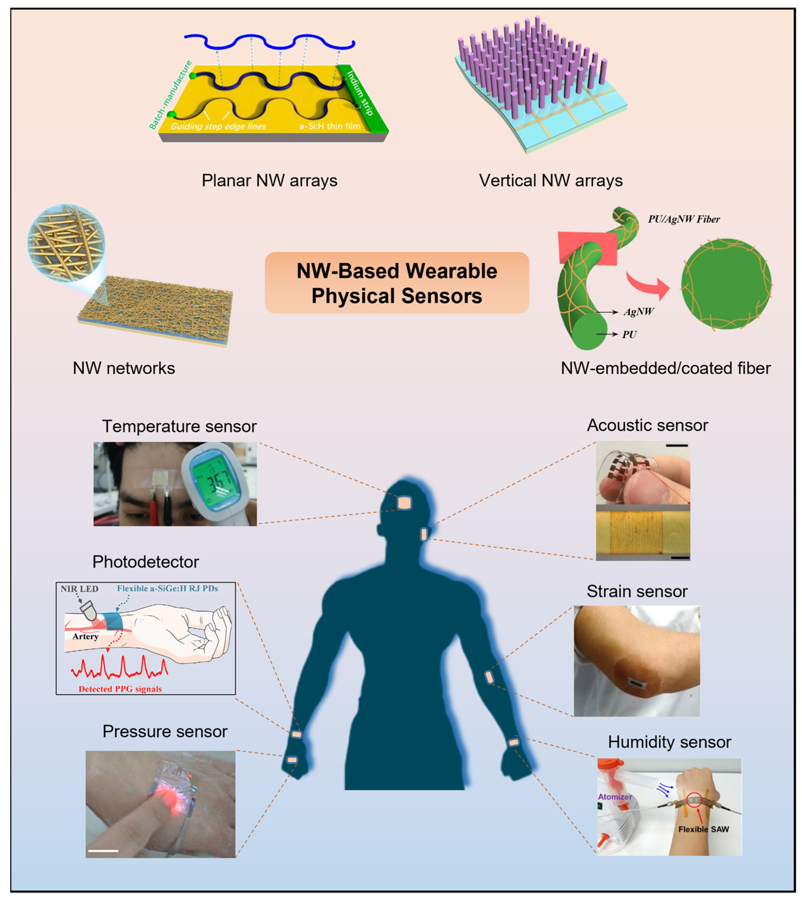
:1. Introduction
2. NW-Based Wearable Mechanical Sensors
2.1. Strain Sensors
- Wide-range capability: Wearable strain sensors should be capable of monitoring large-scale strains occurring in the human body, such as the bending of knee and elbow joints. This ensures the sensor’s ability to capture and measure significant deformations accurately.
- High sensitivity: Strain sensors need to possess high sensitivity to detect small-scale strains in the human body, such as facial expressions. This sensitivity allows for precise and reliable monitoring of subtle movements and micro deformations.
- Fast response and recovery time: A desirable characteristic of strain sensors for wearable applications is a short response and recovery time. This ensures real-time monitoring capabilities, enabling immediate feedback and data acquisition.
2.1.1. Resistive Strain Sensors

| Authors | Sensing Mechanism | Materials | Maximum Sensitivity | Stretchability | Durability | Features |
|---|---|---|---|---|---|---|
| Zhang et al. [51] | Resistive | AgNWs/PDMS | 623.2 | 35% | >2000 | High sensitivity |
| Kong et al. [64] | Resistive | AgNWs/PDMS | 3 | 100% | >6000 | Fibrous sensor, High stretchability |
| Du et al. [65] | Capacitive | AgNWs/Mxene/TPU | 1.21 | 270% | >2000 | Prepared by a whole electrospinning procedure |
| Kim et al. [49] | Capacitive | AgNWs/PDMS | 1.57 | 100% | >1000 | Transparent |

2.1.2. Capacitive Strain Sensors
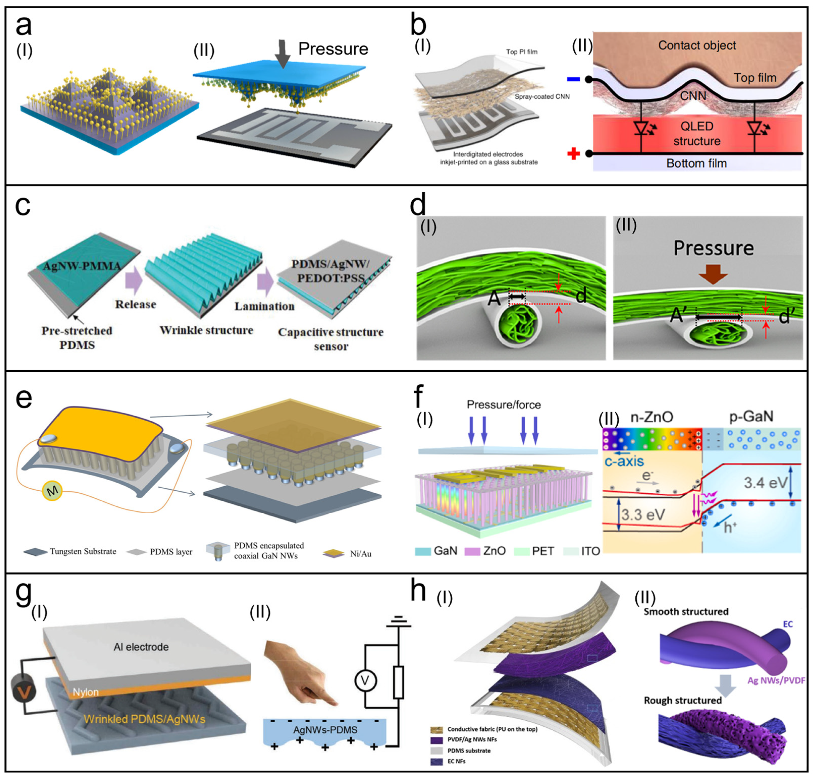
2.2. Pressure Sensors
- Resistive pressure sensors: These sensors convert pressure input into changes in resistance. By measuring the variations in electrical resistance, they indicate the applied pressure.
- Capacitive pressure sensors: Capacitive sensors transform pressure input into changes in capacitance. They detect alterations in the electrical charge stored in a capacitor, allowing for pressure measurement.
- Piezoelectric pressure sensors: Piezoelectric sensors generate a voltage output in response to applied pressure. They utilize the piezoelectric effect, where certain materials generate an electric charge when subjected to mechanical stress.
- Triboelectric pressure sensors: Triboelectric sensors use the triboelectric effect to convert pressure input into electrical signals. This effect involves the generation of an electric charge through the contact and separation of two different materials.
2.2.1. Resistive Pressure Sensors
2.2.2. Capacitive Pressure Sensors
| Authors | Sensing Mechanism | Materials | Maximum Sensitivity | Response Time | Durability | Features |
|---|---|---|---|---|---|---|
| Zhu et al. [94] | Resistive | AuNWs/PDMS | 23 (600 Pa) | <10 ms | >10,000 | High sensitivity in a low-pressure regime |
| Lee et al. [50] | Resistive | Te-PEDOT:PSS NWs/PI | >5000 | <1 ms | >14,000 | High spatial resolution, Transparent |
| Chen et al. [98] | Capacitive | AgNWs/PDMS | 2.76 | <150 ms | >1000 | Low detection limit |
| Guan et al. [99] | Capacitive | AgNWs/PDMS | 5.49 | <75 ms | >2000 | Fibrous sensor, Proximity sensing |
| Waseem et al. [100] | Piezoelectric | GaNNWs/PDMS | 14.25 V/kPa | <55 ms | >250,000 | Capability to detect static pressure, Self-powered |
| Kang et al. [101] | Triboelectric | AgNWs/PDMS | 1.187 V/kPa | <30 ms | >900 | Self-powered |
2.2.3. Piezoelectric/Piezo-Phototronic Pressure Sensors
2.2.4. Triboelectric Pressure Sensors
2.3. Challenges and Future Opportunities
3. NW-Based Wearable Photodetectors
3.1. Photoconductors
| Authors | Sensing Materials | Wavelength (nm) | ) | Specific Detectivity (Jones) | Rise Time/Fall Time (ms) | External Quantum Efficiency (%) |
|---|---|---|---|---|---|---|
| Yalagala et al. [118] | ZnO NWs | 365 | 55 | 700/800 | ||
| Zhang et al. [122] | S-GaSb NWs | 1550 | 939 | 50 | ||
| Ren et al. [127] | GaSb NWs | 1550 | 77.3 | |||
| Li et al. [121] | Te@TeSe NWs | 1550 | 2500/2000 | |||
| Zhang et al. [56] | a-SiGe:H NWs | 800 | 0.14 | 3.6/13.2 | ||
| Peng et al. [124] | GaN/ZnO NWs | 325 | 2.82 | 6.9/6.4 |
3.2. Photodiodes
3.3. Challenges and Future Opportunities
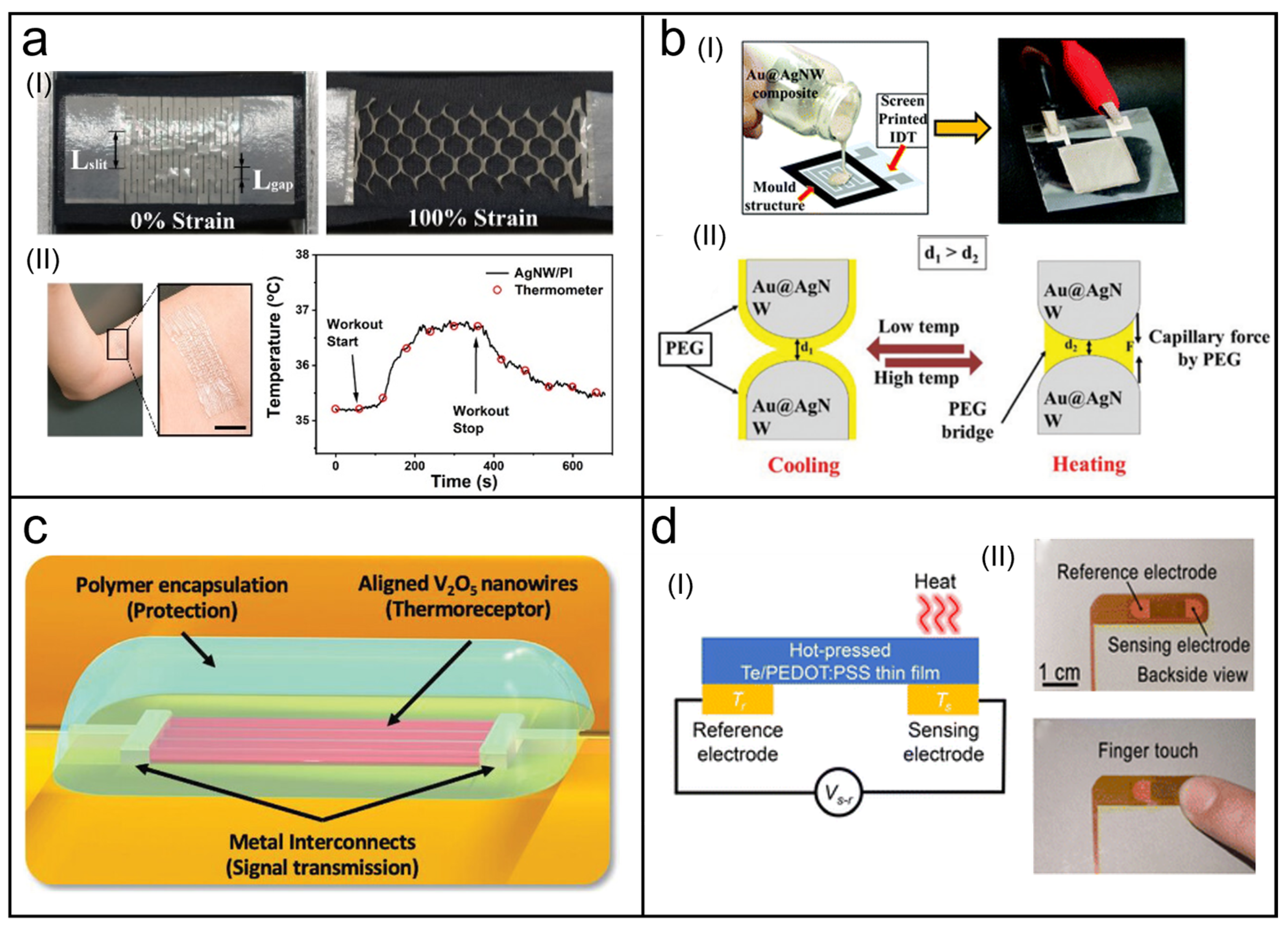
4. NW-Based Wearable Temperature Sensors
4.1. Thermoresistive Temperature Sensors
4.2. Thermoelectric Temperature Sensors
4.3. Challenges and Future Opportunities
| Authors | Sensing Materials | Structure Type | Sensitivity | Response Time |
|---|---|---|---|---|
| Jo et al. [132] | AgNWs, metal-plated (Cu or Ni) nanofibers | Network | ||
| Cui et al. [133] | AgNWs | Network | ||
| Kumar et al. [55] | Au@AgNWs, PEG | Network | <100 s | |
| Neto et al. [134] | V2O5 NWs | Planar arrays | 1 s | |
| Zeng et al. [137] | Ag2Te NWs | Network | 1.05 s | |
| Li et al. [135] | TeNWs, PEDOT:PSS | Network | 1.8 s |
5. Other Types of NW-Based Wearable Physical Sensors
6. NW-Based Multifunctional Wearable Physical Sensors
6.1. Multifunctional Single Wearable Physical Sensors
6.2. Multifunctional Integrated Wearable Physical Sensors

6.3. Challenges and Future Opportunities
7. Conclusions and Perspectives
- Preparation and assembly methods of NWs
- Structural design of NWs and sensors
- Sensing mechanism
- Other issues worth considering
Author Contributions
Funding
Institutional Review Board Statement
Informed Consent Statement
Data Availability Statement
Conflicts of Interest
References
- Wang, X.; Liu, Z.; Zhang, T. Flexible Sensing Electronics for Wearable/Attachable Health Monitoring. Small 2017, 13, 1602790. [Google Scholar] [CrossRef] [PubMed]
- Cheng, X.; Zhang, F.; Bo, R.; Shen, Z.; Pang, W.; Jin, T.; Song, H.; Xue, Z.; Zhang, Y. An Anti-Fatigue Design Strategy for 3D Ribbon-Shaped Flexible Electronics. Adv. Mater. 2021, 33, 2102684. [Google Scholar] [CrossRef] [PubMed]
- Jia, S.; Gao, H.; Xue, Z.; Meng, X. Recent advances in multifunctional wearable sensors and systems: Design, fabrication, and applications. Biosensors 2022, 12, 1057. [Google Scholar] [CrossRef] [PubMed]
- Yin, R.; Wang, D.; Zhao, S.; Lou, Z.; Shen, G. Wearable Sensors-Enabled Human–Machine Interaction Systems: From Design to Application. Adv. Funct. Mater. 2021, 31, 2008936. [Google Scholar] [CrossRef]
- Wang, K.; Yap, L.W.; Gong, S.; Wang, R.; Wang, S.; Cheng, W. Nanowire-Based Soft Wearable Human–Machine Interfaces for Future Virtual and Augmented Reality Applications. Adv. Funct. Mater. 2021, 31, 2008347. [Google Scholar] [CrossRef]
- Xue, Z.; Zhao, J. Bioelectric Interface Technologies in Cells and Organoids. Adv. Mater. Interfaces 2023, 2300550. [Google Scholar] [CrossRef]
- Song, H.; Luo, G.; Ji, Z.; Bo, R.; Xue, Z.; Yan, D.; Zhang, F.; Bai, K.; Liu, J.; Cheng, X.; et al. Highly-integrated, miniaturized, stretchable electronic systems based on stacked multilayer network materials. Sci. Adv. 2022, 8, eabm3785. [Google Scholar] [CrossRef] [PubMed]
- Shi, Q.; Dong, B.; He, T.; Sun, Z.; Zhu, J.; Zhang, Z.; Lee, C. Progress in wearable electronics/photonics—Moving toward the era of artificial intelligence and internet of things. InfoMat 2020, 2, 1131–1162. [Google Scholar] [CrossRef]
- Ji, Z.; Zhao, J.; Song, H.; Xu, S.; Pang, W.; Hu, X.; Zhang, F.; Jin, T.; Shuai, Y.; Lan, Y.; et al. Morphable three-dimensional electronic mesofliers capable of on-demand unfolding. Sci. China Mater. 2022, 65, 2309–2318. [Google Scholar] [CrossRef]
- Xue, Z.; Song, H.; Rogers, J.A.; Zhang, Y.; Huang, Y. Mechanically-Guided Structural Designs in Stretchable Inorganic Electronics. Adv. Mater. 2020, 32, 1902254. [Google Scholar] [CrossRef]
- Zhang, F.; Jin, T.; Xue, Z.; Zhang, Y. Recent progress in three-dimensional flexible physical sensors. Int. J. Smart Nano Mater. 2022, 13, 17–41. [Google Scholar] [CrossRef]
- Ma, Q.; Zhang, Y. Mechanics of Fractal-Inspired Horseshoe Microstructures for Applications in Stretchable Electronics. J. Appl. Mech. 2016, 83, 111008. [Google Scholar] [CrossRef]
- Ma, Q.; Cheng, H.; Jang, K.-I.; Luan, H.; Hwang, K.-C.; Rogers, J.A.; Huang, Y.; Zhang, Y. A nonlinear mechanics model of bio-inspired hierarchical lattice materials consisting of horseshoe microstructures. J. Mech. Phys. Solids 2016, 90, 179–202. [Google Scholar] [CrossRef] [PubMed]
- Zhang, Y.; Zhang, F.; Yan, Z.; Ma, Q.; Li, X.; Huang, Y.; Rogers, J.A. Printing, folding and assembly methods for forming 3D mesostructures in advanced materials. Nat. Rev. Mater. 2017, 2, 17019. [Google Scholar] [CrossRef]
- Guo, X.; Xue, Z.; Zhang, Y. Manufacturing of 3D multifunctional microelectronic devices: Challenges and opportunities. NPG Asia Mater. 2019, 11, 29. [Google Scholar] [CrossRef]
- Xue, Z.; Jin, T.; Xu, S.; Bai, K.; He, Q.; Zhang, F.; Cheng, X.; Ji, Z.; Pang, W.; Shen, Z.; et al. Assembly of complex 3D structures and electronics on curved surfaces. Sci. Adv. 2022, 8, eabm6922. [Google Scholar] [CrossRef] [PubMed]
- Li, K.; Shuai, Y.; Cheng, X.; Luan, H.; Liu, S.; Yang, C.; Xue, Z.; Huang, Y.; Zhang, Y. Island Effect in Stretchable Inorganic Electronics. Small 2022, 18, 2107879. [Google Scholar] [CrossRef]
- Christensen, R.M. Review of the Basic Elastic Mechanical Properties and Their Realignment to Establish Ductile Versus Brittle Failure Behaviors. Appl. Mech. Rev. 2023, 75, 030801. [Google Scholar] [CrossRef]
- Dal, H.; Açıkgöz, K.; Badienia, Y. On the performance of isotropic hyperelastic constitutive models for rubber-like materials: A state of the art review. Appl. Mech. Rev. 2021, 73, 020802. [Google Scholar] [CrossRef]
- Mogilevskaya, S.G.; Zemlyanova, A.Y.; Kushch, V.I. Fiber-and particle-reinforced composite materials with the Gurtin–Murdoch and Steigmann–Ogden surface energy endowed interfaces. Appl. Mech. Rev. 2021, 73, 050801. [Google Scholar] [CrossRef]
- Yang, S.; Sharma, P. A tutorial on the stability and bifurcation analysis of the electromechanical behaviour of soft materials. Appl. Mech. Rev. 2023, 75, 044801. [Google Scholar] [CrossRef]
- Vaghasiya, J.V.; Mayorga-Martinez, C.C.; Pumera, M. Wearable sensors for telehealth based on emerging materials and nanoarchitectonics. npj Flex. Electron. 2023, 7, 26. [Google Scholar] [CrossRef] [PubMed]
- Koh, E.H.; Lee, W.-C.; Choi, Y.-J.; Moon, J.-I.; Jang, J.; Park, S.-G.; Choo, J.; Kim, D.-H.; Jung, H.S. A wearable surface-enhanced Raman scattering sensor for label-free molecular detection. ACS Appl. Mater. Interfaces 2021, 13, 3024–3032. [Google Scholar] [CrossRef] [PubMed]
- Ardalan, S.; Hosseinifard, M.; Vosough, M.; Golmohammadi, H. Towards smart personalized perspiration analysis: An IoT-integrated cellulose-based microfluidic wearable patch for smartphone fluorimetric multi-sensing of sweat biomarkers. Biosens. Bioelectron. 2020, 168, 112450. [Google Scholar] [CrossRef] [PubMed]
- Ha, T.; Tran, J.; Liu, S.; Jang, H.; Jeong, H.; Mitbander, R.; Huh, H.; Qiu, Y.; Duong, J.; Wang, R.L. A chest-laminated ultrathin and stretchable E-tattoo for the measurement of electrocardiogram, seismocardiogram, and cardiac time intervals. Adv. Sci. 2019, 6, 1900290. [Google Scholar] [CrossRef] [PubMed]
- An, T.; Anaya, D.V.; Gong, S.; Yap, L.W.; Lin, F.; Wang, R.; Yuce, M.R.; Cheng, W. Self-powered gold nanowire tattoo triboelectric sensors for soft wearable human-machine interface. Nano Energy 2020, 77, 105295. [Google Scholar] [CrossRef]
- Luo, J.; Gao, S.; Luo, H.; Wang, L.; Huang, X.; Guo, Z.; Lai, X.; Lin, L.; Li, R.K.; Gao, J. Superhydrophobic and breathable smart MXene-based textile for multifunctional wearable sensing electronics. Chem. Eng. J. 2021, 406, 126898. [Google Scholar] [CrossRef]
- Alshabouna, F.; Lee, H.S.; Barandun, G.; Tan, E.; Çotur, Y.; Asfour, T.; Gonzalez-Macia, L.; Coatsworth, P.; Núnez-Bajo, E.; Kim, J.-S. PEDOT: PSS-modified cotton conductive thread for mass manufacturing of textile-based electrical wearable sensors by computerized embroidery. Mater. Today 2022, 59, 56–67. [Google Scholar] [CrossRef]
- Qiu, A.; Li, P.; Yang, Z.; Yao, Y.; Lee, I.; Ma, J. A Path Beyond Metal and Silicon:Polymer/Nanomaterial Composites for Stretchable Strain Sensors. Adv. Funct. Mater. 2019, 29, 1806306. [Google Scholar] [CrossRef]
- Jayathilaka, W.A.D.M.; Qi, K.; Qin, Y.; Chinnappan, A.; Serrano-García, W.; Baskar, C.; Wang, H.; He, J.; Cui, S.; Thomas, S.W.; et al. Significance of Nanomaterials in Wearables: A Review on Wearable Actuators and Sensors. Adv. Mater. 2019, 31, 1805921. [Google Scholar] [CrossRef]
- Lu, Y.; Biswas, M.C.; Guo, Z.; Jeon, J.-W.; Wujcik, E.K. Recent developments in bio-monitoring via advanced polymer nanocomposite-based wearable strain sensors. Biosens. Bioelectron. 2019, 123, 167–177. [Google Scholar] [CrossRef] [PubMed]
- Zhang, H.; He, R.; Niu, Y.; Han, F.; Li, J.; Zhang, X.; Xu, F. Graphene-enabled wearable sensors for healthcare monitoring. Biosens. Bioelectron. 2022, 197, 113777. [Google Scholar] [CrossRef] [PubMed]
- Qiao, Y.; Li, X.; Hirtz, T.; Deng, G.; Wei, Y.; Li, M.; Ji, S.; Wu, Q.; Jian, J.; Wu, F. Graphene-based wearable sensors. Nanoscale 2019, 11, 18923–18945. [Google Scholar] [CrossRef] [PubMed]
- Cho, S.-Y.; Yu, H.; Choi, J.; Kang, H.; Park, S.; Jang, J.-S.; Hong, H.-J.; Kim, I.-D.; Lee, S.-K.; Jeong, H.S. Continuous meter-scale synthesis of weavable tunicate cellulose/carbon nanotube fibers for high-performance wearable sensors. ACS Nano 2019, 13, 9332–9341. [Google Scholar] [CrossRef] [PubMed]
- Lin, M.; Zheng, Z.; Yang, L.; Luo, M.; Fu, L.; Lin, B.; Xu, C. A high-performance, sensitive, wearable multifunctional sensor based on rubber/CNT for human motion and skin temperature detection. Adv. Mater. 2022, 34, 2107309. [Google Scholar] [CrossRef] [PubMed]
- Zhang, J.; Sun, T.; Chen, Y.; Liu, L.; Zhao, H.; Zhang, C.; Meng, X.; Wang, D.; Hu, Z.; Zhang, H.; et al. Nanowires in Flexible Sensors: Structure is Becoming a Key in Controlling the Sensing Performance. Adv. Mater. Technol. 2022, 7, 2200163. [Google Scholar] [CrossRef]
- Sun, Y.; Dong, T.; Yu, L.; Xu, J.; Chen, K. Planar Growth, Integration, and Applications of Semiconducting Nanowires. Adv. Mater. 2020, 32, 1903945. [Google Scholar] [CrossRef] [PubMed]
- Liu, Z.; Yan, J.; Ma, H.; Hu, T.; Wang, J.; Shi, Y.; Xu, J.; Chen, K.; Yu, L. Ab Initio Design, Shaping, and Assembly of Free-Standing Silicon Nanoprobes. Nano Lett. 2021, 21, 2773–2779. [Google Scholar] [CrossRef]
- Cheng, D.; Bai, X.; Pan, J.; Wu, J.; Ran, J.; Cai, G.; Wang, X. In situ hydrothermal growth of Cu NPs on knitted fabrics through polydopamine templates for heating and sensing. Chem. Eng. J. 2020, 382, 123036. [Google Scholar] [CrossRef]
- Li, R.; Zhang, W.; Qin, Y.; Zhang, Y.; Zhu, X.; Li, Y.; Zhu, N.; Hou, C.; Zhang, M. Multifunctional Prussian blue from nano-structure designed to wearable sensors application. TrAC Trends Anal. Chem. 2022, 157, 116729. [Google Scholar] [CrossRef]
- Abid; Sehrawat, P.; Julien, C.; Islam, S. WS2 quantum dots on e-textile as a wearable UV photodetector: How well reduced graphene oxide can serve as a carrier transport medium? ACS Appl. Mater. Interfaces 2020, 12, 39730–39744. [Google Scholar] [CrossRef] [PubMed]
- Kim, J.; Song, S.; Kim, Y.-H.; Park, S.K. Recent progress of quantum dot-based photonic devices and systems: A comprehensive review of materials, devices, and applications. Small Struct. 2021, 2, 2000024. [Google Scholar] [CrossRef]
- Elanjeitsenni, V.P.; Vadivu, K.S.; Prasanth, B.M. A review on thin films, conducting polymers as sensor devices. Mater. Res. Express 2022, 9, 022001. [Google Scholar] [CrossRef]
- Salaheldeen, M.; Méndez, M.; Vega, V.; Fernández, A.; Prida, V.M. Tuning Nanohole Sizes in Ni Hexagonal Antidot Arrays: Large Perpendicular Magnetic Anisotropy for Spintronic Applications. ACS Appl. Nano Mater. 2019, 2, 1866–1875. [Google Scholar] [CrossRef]
- Bilal, M.; Iqbal, H.M.N.; Adil, S.F.; Shaik, M.R.; Abdelgawad, A.; Hatshan, M.R.; Khan, M. Surface-coated magnetic nanostructured materials for robust bio-catalysis and biomedical applications-A review. J. Adv. Res. 2022, 38, 157–177. [Google Scholar] [CrossRef] [PubMed]
- Salaheldeen, M.; Wederni, A.; Ipatov, M.; Zhukova, V.; Lopez Anton, R.; Zhukov, A. Enhancing the Squareness and Bi-Phase Magnetic Switching of Co(2)FeSi Microwires for Sensing Application. Sensors 2023, 23, 5109. [Google Scholar] [CrossRef] [PubMed]
- Alahmadi, M.; Mohamed, W.S.; Zhukov, A.; Salaheldeen, M.; Alsaedi, W.H.; Alhashmialameer, D.; Al-Ghamdi, K.; Abu-Dief, A.M. One-step hydrothermal synthesis of flower-like MoS2/VS2 nanocomposite for biomedical applications. Inorg. Chem. Commun. 2023, 157, 111336. [Google Scholar] [CrossRef]
- Naghdi, M.; Ghovvati, M.; Rabiee, N.; Ahmadi, S.; Abbariki, N.; Sojdeh, S.; Ojaghi, A.; Bagherzadeh, M.; Akhavan, O.; Sharifi, E.; et al. Magnetic nanocomposites for biomedical applications. Adv. Colloid Interface Sci. 2022, 308, 102771. [Google Scholar] [CrossRef]
- Kim, S.-R.; Kim, J.-H.; Park, J.-W. Wearable and Transparent Capacitive Strain Sensor with High Sensitivity Based on Patterned Ag Nanowire Networks. ACS Appl. Mater. Interfaces 2017, 9, 26407–26416. [Google Scholar] [CrossRef]
- Lee, B.; Oh, J.-Y.; Cho, H.; Joo, C.W.; Yoon, H.; Jeong, S.; Oh, E.; Byun, J.; Kim, H.; Lee, S.; et al. Ultraflexible and transparent electroluminescent skin for real-time and super-resolution imaging of pressure distribution. Nat. Commun. 2020, 11, 663. [Google Scholar] [CrossRef]
- Zhang, X.; Li, Z.; Liu, C.; Shan, J.; Guo, X.; Zhao, X.; Ding, J.; Yang, H. Silver Nanowire/Silver/Poly(dimethylsiloxane) as Strain Sensors for Motion Monitoring. ACS Appl. Nano Mater. 2022, 5, 15797–15807. [Google Scholar] [CrossRef]
- Xue, Z.; Sun, M.; Dong, T.; Tang, Z.; Zhao, Y.; Wang, J.; Wei, X.; Yu, L.; Chen, Q.; Xu, J.; et al. Deterministic Line-Shape Programming of Silicon Nanowires for Extremely Stretchable Springs and Electronics. Nano Lett. 2017, 17, 7638–7646. [Google Scholar] [CrossRef] [PubMed]
- Peng, Y.; Que, M.; Lee, H.E.; Bao, R.; Wang, X.; Lu, J.; Yuan, Z.; Li, X.; Tao, J.; Sun, J. Achieving high-resolution pressure mapping via flexible GaN/ZnO nanowire LEDs array by piezo-phototronic effect. Nano Energy 2019, 58, 633–640. [Google Scholar] [CrossRef]
- Zhu, G.-J.; Ren, P.-G.; Guo, H.; Jin, Y.-L.; Yan, D.-X.; Li, Z.-M. Highly Sensitive and Stretchable Polyurethane Fiber Strain Sensors with Embedded Silver Nanowires. ACS Appl. Mater. Interfaces 2019, 11, 23649–23658. [Google Scholar] [CrossRef] [PubMed]
- Kumar, A.; Shaikh, M.O.; Kumar, R.K.R.; Dutt, K.; Pan, C.T.; Chuang, C.H. Highly sensitive, flexible and biocompatible temperature sensor utilizing ultra-long Au@AgNW-based polymeric nanocomposites. Nanoscale 2022, 14, 1742–1754. [Google Scholar] [CrossRef] [PubMed]
- Zhang, S.; Zhang, T.; Liu, Z.; Wang, J.; Xu, J.; Chen, K.; Yu, L. Flexible and Robust 3D a-SiGe Radial Junction Near-Infrared Photodetectors for Rapid Sphygmic Signal Monitoring. Adv. Funct. Mater. 2022, 32, 2107040. [Google Scholar] [CrossRef]
- Gong, S.; Yap, L.W.; Zhu, Y.; Zhu, B.W.; Wang, Y.; Ling, Y.Z.; Zhao, Y.M.; An, T.C.; Lu, Y.R.; Cheng, W.L. A Soft Resistive Acoustic Sensor Based on Suspended Standing Nanowire Membranes with Point Crack Design. Adv. Funct. Mater. 2020, 30, 1910717. [Google Scholar] [CrossRef]
- Han, S.; Liu, C.; Xu, H.; Yao, D.; Yan, K.; Zheng, H.; Chen, H.-J.; Gui, X.; Chu, S.; Liu, C. Multiscale nanowire-microfluidic hybrid strain sensors with high sensitivity and stretchability. npj Flex. Electron. 2018, 2, 16. [Google Scholar] [CrossRef]
- Wu, J.; Yin, C.; Zhou, J.; Li, H.; Liu, Y.; Shen, Y.; Garner, S.; Fu, Y.; Duan, H. Ultrathin Glass-Based Flexible, Transparent, and Ultrasensitive Surface Acoustic Wave Humidity Sensor with ZnO Nanowires and Graphene Quantum Dots. ACS Appl. Mater. Interfaces 2020, 12, 39817–39825. [Google Scholar] [CrossRef]
- Amjadi, M.; Kyung, K.U.; Park, I.; Sitti, M. Stretchable, skin-mountable, and wearable strain sensors and their potential applications: A review. Adv. Funct. Mater. 2016, 26, 1678–1698. [Google Scholar] [CrossRef]
- Choi, S.; Yoon, K.; Lee, S.; Lee, H.J.; Lee, J.; Kim, D.W.; Kim, M.-S.; Lee, T.; Pang, C. Conductive Hierarchical Hairy Fibers for Highly Sensitive, Stretchable, and Water-Resistant Multimodal Gesture-Distinguishable Sensor, VR Applications. Adv. Funct. Mater. 2019, 29, 1905808. [Google Scholar] [CrossRef]
- Cheng, R.; Zeng, J.; Wang, B.; Li, J.; Cheng, Z.; Xu, J.; Gao, W.; Chen, K. Ultralight, flexible and conductive silver nanowire/nanofibrillated cellulose aerogel for multifunctional strain sensor. Chem. Eng. J. 2021, 424, 130565. [Google Scholar] [CrossRef]
- Yin, R.; Yang, S.; Li, Q.; Zhang, S.; Liu, H.; Han, J.; Liu, C.; Shen, C. Flexible conductive Ag nanowire/cellulose nanofibril hybrid nanopaper for strain and temperature sensing applications. Sci. Bull. 2020, 65, 899–908. [Google Scholar] [CrossRef]
- Kong, W.-W.; Zhou, C.-G.; Dai, K.; Jia, L.-C.; Yan, D.-X.; Li, Z.-M. Highly stretchable and durable fibrous strain sensor with growth ring-like spiral structure for wearable electronics. Compos. Part B Eng. 2021, 225, 109275. [Google Scholar] [CrossRef]
- Du, H.; Zhou, H.; Wang, M.; Zhao, G.; Jin, X.; Liu, H.; Chen, W.; Weng, W.; Ma, A. Electrospun Elastic Films Containing AgNW-Bridged MXene Networks as Capacitive Electronic Skins. ACS Appl. Mater. Interfaces 2022, 14, 31225–31233. [Google Scholar] [CrossRef] [PubMed]
- Zhu, Y.; Wei, Q.; Jin, Q.; Li, G.; Zhang, Q.; Xiao, H.; Li, T.; Wei, F.; Luo, Y. Polyethylene Glycol Functionalized Silicon Nanowire Field-Effect Transistor Biosensor for Glucose Detection. Nanomaterials 2023, 13, 604. [Google Scholar] [CrossRef] [PubMed]
- Hu, J.; Li, Y.; Zhang, X.; Wang, Y.; Zhang, J.; Yan, J.; Li, J.; Zhang, Z.; Yin, H.; Wei, Q.; et al. Ultrasensitive Silicon Nanowire Biosensor with Modulated Threshold Voltages and Ultra-Small Diameter for Early Kidney Failure Biomarker Cystatin C. Biosensors 2023, 13, 645. [Google Scholar] [CrossRef]
- Cox, L.M.; Martinez, A.M.; Blevins, A.K.; Sowan, N.; Ding, Y.; Bowman, C.N. Nanoimprint lithography: Emergent materials and methods of actuation. Nano Today 2020, 31, 100838. [Google Scholar] [CrossRef]
- Kim, K.; Ki, B.; Choi, K.; Oh, J. Anodic Imprint Lithography: Direct Imprinting of Single Crystalline GaAs with Anodic Stamp. ACS Nano 2019, 13, 13465–13473. [Google Scholar] [CrossRef]
- Rothman, A.; Dubrovskii, V.G.; Joselevich, E. Kinetics and mechanism of planar nanowire growth. Proc. Natl. Acad. Sci. USA 2020, 117, 152–160. [Google Scholar] [CrossRef]
- Ben-Zvi, R.; Burrows, H.; Schvartzman, M.; Bitton, O.; Pinkas, I.; Kaplan-Ashiri, I.; Brontvein, O.; Joselevich, E. In-Plane Nanowires with Arbitrary Shapes on Amorphous Substrates by Artificial Epitaxy. ACS Nano 2019, 13, 5572–5582. [Google Scholar] [CrossRef] [PubMed]
- Tsivion, D.; Schvartzman, M.; Popovitz-Biro, R.; von Huth, P.; Joselevich, E. Guided Growth of Millimeter-Long Horizontal Nanowires with Controlled Orientations. Science 2011, 333, 1003–1007. [Google Scholar] [CrossRef] [PubMed]
- Huang, Y.; Duan, X.; Wei, Q.; Lieber, C.M. Directed Assembly of One-Dimensional Nanostructures into Functional Networks. Science 2001, 291, 630–633. [Google Scholar] [CrossRef] [PubMed]
- Fan, Z.; Ho, J.C.; Jacobson, Z.A.; Yerushalmi, R.; Alley, R.L.; Razavi, H.; Javey, A. Wafer-Scale Assembly of Highly Ordered Semiconductor Nanowire Arrays by Contact Printing. Nano Lett. 2008, 8, 20–25. [Google Scholar] [CrossRef] [PubMed]
- Freer, E.M.; Grachev, O.; Duan, X.; Martin, S.; Stumbo, D.P. High-yield self-limiting single-nanowire assembly with dielectrophoresis. Nat. Nanotechnol. 2010, 5, 525–530. [Google Scholar] [CrossRef] [PubMed]
- Liu, M.; Lagdani, J.; Imrane, H.; Pettiford, C.; Lou, J.; Yoon, S.; Harris, V.G.; Vittoria, C.; Sun, N.X. Self-assembled magnetic nanowire arrays. Appl. Phys. Lett. 2007, 90, 103105. [Google Scholar] [CrossRef]
- Wang, M.C.P.; Gates, B.D. Directed assembly of nanowires. Mater. Today 2009, 12, 34–43. [Google Scholar] [CrossRef]
- Masuda, H.; Fukuda, K. Ordered metal nanohole arrays made by a two-step replication of honeycomb structures of anodic alumina. Science 1995, 268, 1466–1468. [Google Scholar] [CrossRef]
- Xue, Z.; Xu, M.; Li, X.; Wang, J.; Jiang, X.; Wei, X.; Yu, L.; Chen, Q.; Wang, J.; Xu, J.; et al. In-Plane Self-Turning and Twin Dynamics Renders Large Stretchability to Mono-Like Zigzag Silicon Nanowire Springs. Adv. Funct. Mater. 2016, 26, 5352–5359. [Google Scholar] [CrossRef]
- Azrak, E.; Xue, Z.; Liu, S.; Chen, W.; Castro, C.; Duguay, S.; Pareige, P.; Yu, L.; Roca i Cabarrocas, P. Ultrahigh Incorporation of Tin in SiSn Nanowires Grown via In-Plane Solid-Liquid-Solid Mechanism. Appl. Surf. Sci. 2023, 618, 156637. [Google Scholar] [CrossRef]
- Xue, Z.; Chen, W.; Meng, X.; Xu, J.; Shi, Y.; Chen, K.; Yu, L.; Roca i Cabarrocas, P. Precise morphology control of in-plane silicon nanowires via a simple plasma pre-treatment. Appl. Surf. Sci. 2022, 593, 153435. [Google Scholar] [CrossRef]
- Xue, Z.; Xu, M.; Zhao, Y.; Wang, J.; Jiang, X.; Yu, L.; Wang, J.; Xu, J.; Shi, Y.; Chen, K. Engineering island-chain silicon nanowires via a droplet mediated Plateau-Rayleigh transformation. Nat. Commun. 2016, 7, 12836. [Google Scholar] [CrossRef] [PubMed]
- Dong, T.; Sun, Y.; Zhu, Z.; Wu, X.; Wang, J.; Shi, Y.; Xu, J.; Chen, K.; Yu, L. Monolithic Integration of Silicon Nanowire Networks as a Soft Wafer for Highly Stretchable and Transparent Electronics. Nano Lett. 2019, 19, 6235–6243. [Google Scholar] [CrossRef] [PubMed]
- Dai, Y.; Qi, K.; Ou, K.; Song, Y.; Zhou, Y.; Zhou, M.; Song, H.; He, J.; Wang, H.; Wang, R. Ag NW-Embedded Coaxial Nanofiber-Coated Yarns with High Stretchability and Sensitivity for Wearable Multi-Sensing Textiles. ACS Appl. Mater. Interfaces 2023, 15, 11244–11258. [Google Scholar] [CrossRef] [PubMed]
- Zhao, Z.; Li, Q.; Dong, Y.; Gong, J.; Li, Z.; Zhang, J. Washable Patches with Gold Nanowires/Textiles in Wearable Sensors for Health Monitoring. ACS Appl. Mater. Interfaces 2022, 14, 18884–18900. [Google Scholar] [CrossRef] [PubMed]
- Lian, Y.; Yu, H.; Wang, M.; Yang, X.; Zhang, H. Ultrasensitive Wearable Pressure Sensors Based on Silver Nanowire-Coated Fabrics. Nanoscale Res. Lett. 2020, 15, 70. [Google Scholar] [CrossRef] [PubMed]
- Yao, S.; Yang, J.; Poblete, F.R.; Hu, X.; Zhu, Y. Multifunctional Electronic Textiles Using Silver Nanowire Composites. ACS Appl. Mater. Interfaces 2019, 11, 31028–31037. [Google Scholar] [CrossRef]
- Jiang, P.-P.; Qin, H.; Dai, J.; Yu, S.-H.; Cong, H.-P. Ultrastretchable and Self-Healing Conductors with Double Dynamic Network for Omni-Healable Capacitive Strain Sensors. Nano Lett. 2022, 22, 1433–1442. [Google Scholar] [CrossRef]
- Tran, N.-H.; Tran, P.; Lee, J.-H. Copper Nanowire-Sealed Titanium Dioxide/Poly(dimethylsiloxane) Electrode with an In-Plane Wavy Structure for a Stretchable Capacitive Strain Sensor. ACS Appl. Nano Mater. 2022, 5, 7150–7160. [Google Scholar] [CrossRef]
- Yao, S.; Vargas, L.; Hu, X.; Zhu, Y. A Novel Finger Kinematic Tracking Method Based on Skin-Like Wearable Strain Sensors. IEEE Sens. J. 2018, 18, 3010–3015. [Google Scholar] [CrossRef]
- Huang, Y.; Fan, X.; Chen, S.-C.; Zhao, N. Emerging Technologies of Flexible Pressure Sensors: Materials, Modeling, Devices, and Manufacturing. Adv. Funct. Mater. 2019, 29, 1808509. [Google Scholar] [CrossRef]
- dos Santos, A.; Fortunato, E.; Martins, R.; Águas, H.; Igreja, R. Transduction Mechanisms, Micro-Structuring Techniques, and Applications of Electronic Skin Pressure Sensors: A Review of Recent Advances. Sensors 2020, 20, 4407. [Google Scholar] [CrossRef] [PubMed]
- Seesaard, T.; Wongchoosuk, C. Flexible and Stretchable Pressure Sensors: From Basic Principles to State-of-the-Art Applications. Micromachines 2023, 14, 1638. [Google Scholar] [CrossRef] [PubMed]
- Zhu, B.; Ling, Y.; Yap, L.W.; Yang, M.; Lin, F.; Gong, S.; Wang, Y.; An, T.; Zhao, Y.; Cheng, W. Hierarchically Structured Vertical Gold Nanowire Array-Based Wearable Pressure Sensors for Wireless Health Monitoring. ACS Appl. Mater. Interfaces 2019, 11, 29014–29021. [Google Scholar] [CrossRef] [PubMed]
- Jeong, H.; Noh, Y.; Ko, S.H.; Lee, D. Flexible resistive pressure sensor with silver nanowire networks embedded in polymer using natural formation of air gap. Compos. Sci. Technol. 2019, 174, 50–57. [Google Scholar] [CrossRef]
- Gong, S.; Wang, Y.; Yap, L.W.; Ling, Y.; Zhao, Y.; Dong, D.; Shi, Q.; Liu, Y.; Uddin, H.; Cheng, W. A location- and sharpness-specific tactile electronic skin based on staircase-like nanowire patches. Nanoscale Horizons 2018, 3, 640–647. [Google Scholar] [CrossRef] [PubMed]
- Zhu, Y.; Hartel, M.C.; Yu, N.; Garrido, P.R.; Kim, S.; Lee, J.; Bandaru, P.; Guan, S.; Lin, H.; Emaminejad, S.; et al. Epidermis-Inspired Wearable Piezoresistive Pressure Sensors Using Reduced Graphene Oxide Self-Wrapped Copper Nanowire Networks. Small Methods 2022, 6, 2100900. [Google Scholar] [CrossRef] [PubMed]
- Chen, S.; Peng, S.; Sun, W.; Gu, G.; Zhang, Q.; Guo, X. Scalable Processing Ultrathin Polymer Dielectric Films with a Generic Solution Based Approach for Wearable Soft Electronics. Adv. Mater. Technol. 2019, 4, 1800681. [Google Scholar] [CrossRef]
- Guan, F.; Xie, Y.; Wu, H.; Meng, Y.; Shi, Y.; Gao, M.; Zhang, Z.; Chen, S.; Chen, Y.; Wang, H.; et al. Silver Nanowire–Bacterial Cellulose Composite Fiber-Based Sensor for Highly Sensitive Detection of Pressure and Proximity. ACS Nano 2020, 14, 15428–15439. [Google Scholar] [CrossRef]
- Waseem, A.; Johar, M.A.; Hassan, M.A.; Bagal, I.V.; Abdullah, A.; Ha, J.-S.; Lee, J.K.; Ryu, S.-W. Flexible self-powered piezoelectric pressure sensor based on GaN/p-GaN coaxial nanowires. J. Alloys Compd. 2021, 872, 159661. [Google Scholar] [CrossRef]
- Kang, H.; Zhao, C.; Huang, J.; Ho, D.H.; Megra, Y.T.; Suk, J.W.; Sun, J.; Wang, Z.L.; Sun, Q.; Cho, J.H. Fingerprint-Inspired Conducting Hierarchical Wrinkles for Energy-Harvesting E-Skin. Adv. Funct. Mater. 2019, 29, 1903580. [Google Scholar] [CrossRef]
- Lou, M.; Abdalla, I.; Zhu, M.; Yu, J.; Li, Z.; Ding, B. Hierarchically Rough Structured and Self-Powered Pressure Sensor Textile for Motion Sensing and Pulse Monitoring. ACS Appl. Mater. Interfaces 2020, 12, 1597–1605. [Google Scholar] [CrossRef] [PubMed]
- Hsieh, G.-W.; Shih, L.-C.; Chen, P.-Y. Porous Polydimethylsiloxane Elastomer Hybrid with Zinc Oxide Nanowire for Wearable, Wide-Range, and Low Detection Limit Capacitive Pressure Sensor. Nanomaterials 2022, 12, 256. [Google Scholar] [CrossRef] [PubMed]
- Kumaresan, Y.; Ma, S.; Ozioko, O.; Dahiya, R. Soft Capacitive Pressure Sensor With Enhanced Sensitivity Assisted by ZnO NW Interlayers and Airgap. IEEE Sens. J. 2022, 22, 3974–3982. [Google Scholar] [CrossRef]
- Nie, K.; Wang, Z.; Zhou, H.; Tang, R.; Shen, X.; Sun, Q. Improved dielectricity of anisotropic wood slices and bioinspired micropatterned film electrodes for highly sensitive flexible electronic sensors. J. Mater. Chem. C 2020, 8, 16113–16120. [Google Scholar] [CrossRef]
- Wang, P.; Li, G.; Liu, J.; Hou, Z.; Meng, C.; Guo, S.; Liu, C.; Fan, S. Tailorable Capacitive Tactile Sensor Based on Stretchable and Dissolvable Porous Silver Nanowire/Polyvinyl Alcohol Nanocomposite Hydrogel for Wearable Human Motion Detection. Adv. Mater. Interfaces 2021, 8, 2100998. [Google Scholar] [CrossRef]
- Kang, B.-C.; Park, S.-J.; Ha, T.-J. Wearable Pressure/Touch Sensors Based on Hybrid Dielectric Composites of Zinc Oxide Nanowires/Poly(dimethylsiloxane) and Flexible Electrodes of Immobilized Carbon Nanotube Random Networks. ACS Appl. Mater. Interfaces 2021, 13, 42014–42023. [Google Scholar] [CrossRef] [PubMed]
- Zhao, Q.-L.; He, G.-P.; Di, J.-J.; Song, W.-L.; Hou, Z.-L.; Tan, P.-P.; Wang, D.-W.; Cao, M.-S. Flexible semitransparent energy harvester with high pressure sensitivity and power density based on laterally aligned PZT single-crystal nanowires. ACS Appl. Mater. Interfaces 2017, 9, 24696–24703. [Google Scholar] [CrossRef]
- Rim, Y.S.; Bae, S.H.; Chen, H.; De Marco, N.; Yang, Y. Recent progress in materials and devices toward printable and flexible sensors. Adv. Mater. 2016, 28, 4415–4440. [Google Scholar] [CrossRef]
- Jesionek, M.; Toroń, B.; Szperlich, P.; Biniaś, W.; Biniaś, D.; Rabiej, S.; Starczewska, A.; Nowak, M.; Kępińska, M.; Dec, J. Fabrication of a new PVDF/SbSI nanowire composite for smart wearable textile. Polymer 2019, 180, 121729. [Google Scholar] [CrossRef]
- Lee, E.; Park, J.; Yim, M.; Jeong, S.; Yoon, G. High-efficiency micro-energy generation based on free-carrier-modulated ZnO:N piezoelectric thin films. Appl. Phys. Lett. 2014, 104, 213908. [Google Scholar] [CrossRef]
- Zhang, P.; Deng, L.; Zhang, H.; He, J.; Fan, X.; Ma, Y. Enhanced Performance of Triboelectric Nanogenerator with Micro-Rhombic Patterned PDMS for Self-Powered Wearable Sensing. Adv. Mater. Interfaces 2022, 9, 2201265. [Google Scholar] [CrossRef]
- Kim, W.-G.; Kim, D.-W.; Tcho, I.-W.; Kim, J.-K.; Kim, M.-S.; Choi, Y.-K. Triboelectric Nanogenerator: Structure, Mechanism, and Applications. ACS Nano 2021, 15, 258–287. [Google Scholar] [CrossRef] [PubMed]
- Cheng, T.; Shao, J.; Wang, Z.L. Triboelectric nanogenerators. Nat. Rev. Methods Primers 2023, 3, 39. [Google Scholar] [CrossRef]
- Peng, X.; Dong, K.; Ye, C.; Jiang, Y.; Zhai, S.; Cheng, R.; Liu, D.; Gao, X.; Wang, J.; Wang, Z.L. A breathable, biodegradable, antibacterial, and self-powered electronic skin based on all-nanofiber triboelectric nanogenerators. Sci. Adv. 2020, 6, eaba9624. [Google Scholar] [CrossRef] [PubMed]
- Fan, F.-R.; Lin, L.; Zhu, G.; Wu, W.; Zhang, R.; Wang, Z.L. Transparent Triboelectric Nanogenerators and Self-Powered Pressure Sensors Based on Micropatterned Plastic Films. Nano Lett. 2012, 12, 3109–3114. [Google Scholar] [CrossRef] [PubMed]
- Lien, D.-H.; Wang, H.-P.; Chen, S.-B.; Chi, Y.-C.; Wu, C.-L.; Lin, G.-R.; Liao, Y.-C.; He, J.-H. 360° omnidirectional, printable and transparent photodetectors for flexible optoelectronics. npj Flex. Electron. 2018, 2, 19. [Google Scholar] [CrossRef]
- Yalagala, B.P.; Dahiya, A.S.; Dahiya, R. ZnO nanowires based degradable high-performance photodetectors for eco-friendly green electronics. Opto-Electron. Adv. 2023, 6, 220020. [Google Scholar] [CrossRef]
- Gu, L.; Poddar, S.; Lin, Y.; Long, Z.; Zhang, D.; Zhang, Q.; Shu, L.; Qiu, X.; Kam, M.; Javey, A.; et al. A biomimetic eye with a hemispherical perovskite nanowire array retina. Nature 2020, 581, 278–282. [Google Scholar] [CrossRef]
- Li, L.; Gu, L.; Lou, Z.; Fan, Z.; Shen, G. ZnO Quantum Dot Decorated Zn2SnO4 Nanowire Heterojunction Photodetectors with Drastic Performance Enhancement and Flexible Ultraviolet Image Sensors. ACS Nano 2017, 11, 4067–4076. [Google Scholar] [CrossRef]
- Li, L.; Wang, D.; Zhang, D.; Ran, W.; Yan, Y.; Li, Z.; Wang, L.; Shen, G. Near-Infrared Light Triggered Self-Powered Mechano-Optical Communication System using Wearable Photodetector Textile. Adv. Funct. Mater. 2021, 31, 2104782. [Google Scholar] [CrossRef]
- Zhang, K.; Ren, Z.; Cao, H.; Li, L.; Wang, Y.; Zhang, W.; Li, Y.; Yang, H.; Meng, Y.; Ho, J.C.; et al. Near-Infrared Polarimetric Image Sensors Based on Ordered Sulfur-Passivation GaSb Nanowire Arrays. ACS Nano 2022, 16, 8128–8140. [Google Scholar] [CrossRef] [PubMed]
- Wu, D.; Zhang, Y.; Liu, C.; Sun, Z.; Wang, Z.; Lin, Z.; Qiu, M.; Fu, D.; Wang, K. Recent Progress of Narrowband Perovskite Photodetectors: Fundamental Physics and Strategies. Adv. Devices Instrum. 2023, 4, 0006. [Google Scholar] [CrossRef]
- Peng, Y.; Lu, J.; Wang, X.; Ma, W.; Que, M.; Chen, Q.; Li, F.; Liu, X.; Gao, W.; Pan, C. Self-powered high-performance flexible GaN/ZnO heterostructure UV photodetectors with piezo-phototronic effect enhanced photoresponse. Nano Energy 2022, 94, 106945. [Google Scholar] [CrossRef]
- Sun, J.; Peng, M.; Zhang, Y.; Zhang, L.; Peng, R.; Miao, C.; Liu, D.; Han, M.; Feng, R.; Ma, Y.; et al. Ultrahigh Hole Mobility of Sn-Catalyzed GaSb Nanowires for High Speed Infrared Photodetectors. Nano Lett. 2019, 19, 5920–5929. [Google Scholar] [CrossRef] [PubMed]
- Yang, Z.-x.; Yip, S.; Li, D.; Han, N.; Dong, G.; Liang, X.; Shu, L.; Hung, T.F.; Mo, X.; Ho, J.C. Approaching the Hole Mobility Limit of GaSb Nanowires. ACS Nano 2015, 9, 9268–9275. [Google Scholar] [CrossRef] [PubMed]
- Ren, Z.; Wang, P.; Zhang, K.; Ran, W.; Yang, J.; Liu, Y.-Y.; Lou, Z.; Shen, G.; Wei, Z. Short-Wave Near-Infrared Polarization Sensitive Photodetector Based on GaSb Nanowire. IEEE Electron. Device Lett. 2021, 42, 549–552. [Google Scholar] [CrossRef]
- Bi, S.; Li, Q.; He, Z.; Guo, Q.; Asare-Yeboah, K.; Liu, Y.; Jiang, C. Highly enhanced performance of integrated piezo photo-transistor with dual inverted OLED gate and nanowire array channel. Nano Energy 2019, 66, 104101. [Google Scholar] [CrossRef]
- Pan, C.; Zhai, J.; Wang, Z.L. Piezotronics and Piezo-phototronics of Third Generation Semiconductor Nanowires. Chem. Rev. 2019, 119, 9303–9359. [Google Scholar] [CrossRef]
- Wang, P.; Lan, Y.; Huan, C.; Luo, J.; Cai, W.; Fan, J.; He, X.; Huang, Z.; Zhu, L.; Ke, Q.; et al. Recent progress on performance-enhancing strategies in flexible photodetectors: From structural engineering to flexible integration. Mater. Sci. Eng. R Rep. 2023, 156, 100759. [Google Scholar] [CrossRef]
- Ha, H.; Suryaprabha, T.; Choi, C.; Chandio, Z.A.; Kim, B.; Lim, S.; Cheong, J.Y.; Hwang, B. Recent research trends in textile-based temperature sensors: A mini review. Nanotechnology 2023, 34, 422001. [Google Scholar] [CrossRef]
- Jo, H.S.; Kwon, H.J.; Kim, T.G.; Park, C.W.; An, S.; Yarin, A.L.; Yoon, S.S. Wearable transparent thermal sensors and heaters based on metal-plated fibers and nanowires. Nanoscale 2018, 10, 19825–19834. [Google Scholar] [CrossRef] [PubMed]
- Cui, Z.; Poblete, F.R.; Zhu, Y. Tailoring the Temperature Coefficient of Resistance of Silver Nanowire Nanocomposites and their Application as Stretchable Temperature Sensors. ACS Appl. Mater. Interfaces 2019, 11, 17836–17842. [Google Scholar] [CrossRef] [PubMed]
- Neto, J.; Chirila, R.; Dahiya, A.S.; Christou, A.; Shakthivel, D.; Dahiya, R. Skin-Inspired Thermoreceptors-Based Electronic Skin for Biomimicking Thermal Pain Reflexes. Adv. Sci. 2022, 9, e2201525. [Google Scholar] [CrossRef] [PubMed]
- Li, M.; Xiong, Y.; Wei, H.; Yao, F.; Han, Y.; Du, Y.; Xu, D. Flexible Te/PEDOT:PSS thin films with high thermoelectric power factor and their application as flexible temperature sensors. Nanoscale 2023, 15, 11237–11246. [Google Scholar] [CrossRef] [PubMed]
- Neto, J.; Dahiya, A.S.; Kumaresan, Y.; Shakthivel, D.; Dahiya, R. V2O5 Nanowires-Based Flexible Temperature Sensor. In Proceedings of the 2021 IEEE International Conference on Flexible and Printable Sensors and Systems (FLEPS), Manchester, UK, 20–23 June 2021; pp. 1–4. [Google Scholar]
- Zeng, X.; Yan, C.; Ren, L.; Zhang, T.; Zhou, F.; Liang, X.; Wang, N.; Sun, R.; Xu, J.-B.; Wong, C.-P. Silver Telluride Nanowire Assembly for High-Performance Flexible Thermoelectric Film and Its Application in Self-Powered Temperature Sensor. Adv. Electron. Mater. 2019, 5, 1800612. [Google Scholar] [CrossRef]
- Du, M.; Ouyang, J.; Zhang, K. Flexible Bi2Te3/PEDOT nanowire sandwich-like films towards high-performance wearable cross-plane thermoelectric generator and temperature sensor array. J. Mater. Chem. A 2023, 11, 16039–16048. [Google Scholar] [CrossRef]
- Huang, S.; Zhang, B.; Lin, Y.; Lee, C.-S.; Zhang, X. Compact Biomimetic Hair Sensors Based on Single Silicon Nanowires for Ultrafast and Highly-Sensitive Airflow Detection. Nano Lett. 2021, 21, 4684–4691. [Google Scholar] [CrossRef]
- Yap, L.W.; Shi, Q.; Gong, S.; Wang, Y.; Chen, Y.; Zhu, C.; Gu, Z.; Suzuki, K.; Zhu, Y.; Cheng, W. Bifunctional Fe3O4@AuNWs particle as wearable bending and strain sensor. Inorg. Chem. Commun. 2019, 104, 98–104. [Google Scholar] [CrossRef]
- Lee, S.; Kim, J.; Yun, I.; Bae, G.Y.; Kim, D.; Park, S.; Yi, I.-M.; Moon, W.; Chung, Y.; Cho, K. An ultrathin conformable vibration-responsive electronic skin for quantitative vocal recognition. Nat. Commun. 2019, 10, 2468. [Google Scholar] [CrossRef]
- Kang, S.; Cho, S.; Shanker, R.; Lee, H.; Park, J.; Um, D.-S.; Lee, Y.; Ko, H. Transparent and conductive nanomembranes with orthogonal silver nanowire arrays for skin-attachable loudspeakers and microphones. Sci. Adv. 2018, 4, eaas8772. [Google Scholar] [CrossRef] [PubMed]
- Lang, C.; Fang, J.; Shao, H.; Ding, X.; Lin, T. High-sensitivity acoustic sensors from nanofibre webs. Nat. Commun. 2016, 7, 11108. [Google Scholar] [CrossRef] [PubMed]
- Zhang, Q.; Du, Y.; Sun, Y.; Zhuo, K.; Ji, J.; Yuan, Z.; Zhang, W.; Sang, S. A Flexible Magnetic Field Sensor Based on AgNWs & MNs-PDMS. Nanoscale Res. Lett. 2019, 14, 27. [Google Scholar] [CrossRef] [PubMed]
- Hu, T.; Xuan, S.; Ding, L.; Gong, X. Stretchable and magneto-sensitive strain sensor based on silver nanowire-polyurethane sponge enhanced magnetorheological elastomer. Mater. Design 2018, 156, 528–537. [Google Scholar] [CrossRef]
- Su, D.; Um, J.; Moreno, J.; Nemati, Z.; Srinivasan, K.; Chen, J.; Zamani Kouhpanji, M.R.; Shore, D.; Wu, K.; Kosel, J.; et al. GMR biosensing with magnetic nanowires as labels for the detection of osteosarcoma cells. Sens. Actuators A Phys. 2023, 350, 114115. [Google Scholar] [CrossRef]
- Zamani Kouhpanji, M.R.; Nemati, Z.; Mahmoodi, M.M.; Um, J.; Modiano, J.; Franklin, R.; Stadler, B. Selective Detection of Cancer Cells Using Magnetic Nanowires. ACS Appl. Mater. Interfaces 2021, 13, 21060–21066. [Google Scholar] [CrossRef] [PubMed]
- Chen, Y.; Bai, Y.; Wang, X.; Zhang, H.; Zheng, H.; Gu, N. Plasmonic/magnetic nanoarchitectures: From controllable design to biosensing and bioelectronic interfaces. Biosens. Bioelectron. 2023, 219, 114744. [Google Scholar] [CrossRef] [PubMed]
- Zhen, Z.; Li, Z.; Zhao, X.; Zhong, Y.; Zhang, L.; Chen, Q.; Yang, T.; Zhu, H. Formation of Uniform Water Microdroplets on Wrinkled Graphene for Ultrafast Humidity Sensing. Small 2018, 14, e1703848. [Google Scholar] [CrossRef]
- Li, N.; Jiang, Y.; Zhou, C.; Xiao, Y.; Meng, B.; Wang, Z.; Huang, D.; Xing, C.; Peng, Z. High-Performance Humidity Sensor Based on Urchin-Like Composite of Ti3C2 MXene-Derived TiO2 Nanowires. ACS Appl. Mater. Interfaces 2019, 11, 38116–38125. [Google Scholar] [CrossRef]
- Wang, Q.; Ling, S.; Liang, X.; Wang, H.; Lu, H.; Zhang, Y. Self-Healable Multifunctional Electronic Tattoos Based on Silk and Graphene. Adv. Funct. Mater. 2019, 29, 1808695. [Google Scholar] [CrossRef]
- Li, Y.; Han, W. Multifunctional Sensors Based on a Silver Nanowires/PDMS Aerogel Composite. ACS Appl. Electron. Mater. 2022, 4, 5413–5420. [Google Scholar] [CrossRef]
- Deng, H.-T.; Wen, D.-L.; Liu, J.-R.; Zhang, X.-R.; Wang, Y.-L.; Huang, P.; Kim, B.; Zhang, X.-S. Stretchable multifunctional sensor based on porous silver nanowire/silicone rubber conductive film. Nano Res. 2023, 16, 7618–7626. [Google Scholar] [CrossRef]
- Wen, D.-L.; Huang, P.; Li, B.-Y.; Qiu, Y.; Wang, Y.-L.; Zhang, X.-R.; Deng, H.-T.; Zhang, X.-S. Silk fibroin/Ag nanowire-based multifunctional sensor for wearable self-powered wireless multi-sensing microsystems. Nano Energy 2023, 113, 108569. [Google Scholar] [CrossRef]
- Zhang, B.-C.; Jie, J.-S.; Shao, Z.-B.; Huang, S.-Y.; He, L.; Zhang, X.-H. One-step growth of large-area silicon nanowire fabrics for high-performance multifunctional wearable sensors. Nano Res. 2019, 12, 2723–2728. [Google Scholar] [CrossRef]
- Peng, S.; Wu, S.; Yu, Y.; Xia, B.; Lovell, N.H.; Wang, C.H. Multimodal Capacitive and Piezoresistive Sensor for Simultaneous Measurement of Multiple Forces. ACS Appl. Mater. Interfaces 2020, 12, 22179–22190. [Google Scholar] [CrossRef] [PubMed]
- Li, F.; Liu, Y.; Shi, X.; Li, H.; Wang, C.; Zhang, Q.; Ma, R.; Liang, J. Printable and Stretchable Temperature-Strain Dual-Sensing Nanocomposite with High Sensitivity and Perfect Stimulus Discriminability. Nano Lett. 2020, 20, 6176–6184. [Google Scholar] [CrossRef] [PubMed]
- Li, L.; Zhao, S.; Ran, W.; Li, Z.; Yan, Y.; Zhong, B.; Lou, Z.; Wang, L.; Shen, G. Dual sensing signal decoupling based on tellurium anisotropy for VR interaction and neuro-reflex system application. Nat. Commun. 2022, 13, 5975. [Google Scholar] [CrossRef] [PubMed]
- Chen, H.; Lou, Z.; Shen, G. An integrated flexible multifunctional sensing system for simultaneous monitoring of environment signals. Sci. China Mater. 2020, 63, 2560–2569. [Google Scholar] [CrossRef]
- Jo, H.S.; Park, C.-W.; An, S.; Aldalbahi, A.; El-Newehy, M.; Park, S.S.; Yarin, A.L.; Yoon, S.S. Wearable multifunctional soft sensor and contactless 3D scanner using supersonically sprayed silver nanowires, carbon nanotubes, zinc oxide, and PEDOT:PSS. NPG Asia Mater. 2022, 14, 23. [Google Scholar] [CrossRef]
- Gong, S.; Yap, L.W.; Zhu, B.; Zhai, Q.; Liu, Y.; Lyu, Q.; Wang, K.; Yang, M.; Ling, Y.; Lai, D.T.H.; et al. Local Crack-Programmed Gold Nanowire Electronic Skin Tattoos for In-Plane Multisensor Integration. Adv. Mater. 2019, 31, e1903789. [Google Scholar] [CrossRef]
- Kim, T.Y.; Hong, S.H.; Jeong, S.H.; Bae, H.; Cheong, S.; Choi, H.; Hahn, S.K. Multifunctional Intelligent Wearable Devices Using Logical Circuits of Monolithic Gold Nanowires. Adv. Mater. 2023, 35, e2303401. [Google Scholar] [CrossRef]


Disclaimer/Publisher’s Note: The statements, opinions and data contained in all publications are solely those of the individual author(s) and contributor(s) and not of MDPI and/or the editor(s). MDPI and/or the editor(s) disclaim responsibility for any injury to people or property resulting from any ideas, methods, instructions or products referred to in the content. |
© 2023 by the authors. Licensee MDPI, Basel, Switzerland. This article is an open access article distributed under the terms and conditions of the Creative Commons Attribution (CC BY) license (https://creativecommons.org/licenses/by/4.0/).
Share and Cite
Gu, J.; Shen, Y.; Tian, S.; Xue, Z.; Meng, X. Recent Advances in Nanowire-Based Wearable Physical Sensors. Biosensors 2023, 13, 1025. https://doi.org/10.3390/bios13121025
Gu J, Shen Y, Tian S, Xue Z, Meng X. Recent Advances in Nanowire-Based Wearable Physical Sensors. Biosensors. 2023; 13(12):1025. https://doi.org/10.3390/bios13121025
Chicago/Turabian StyleGu, Junlin, Yunfei Shen, Shijia Tian, Zhaoguo Xue, and Xianhong Meng. 2023. "Recent Advances in Nanowire-Based Wearable Physical Sensors" Biosensors 13, no. 12: 1025. https://doi.org/10.3390/bios13121025