
Optimization of Piezoresistive Strain Sensors Based on Gold Nanoparticle Deposits on PDMS Substrates for Highly Sensitive Human Pulse Sensing

 ,
,  and
and 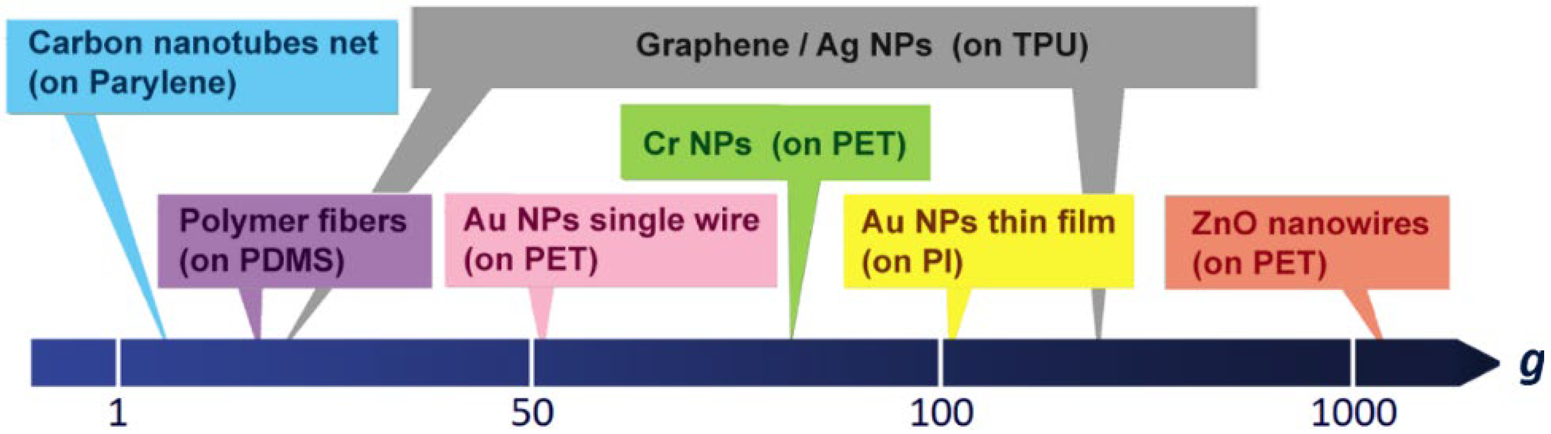
Abstract
:1. Introduction
2. Experimental Procedures
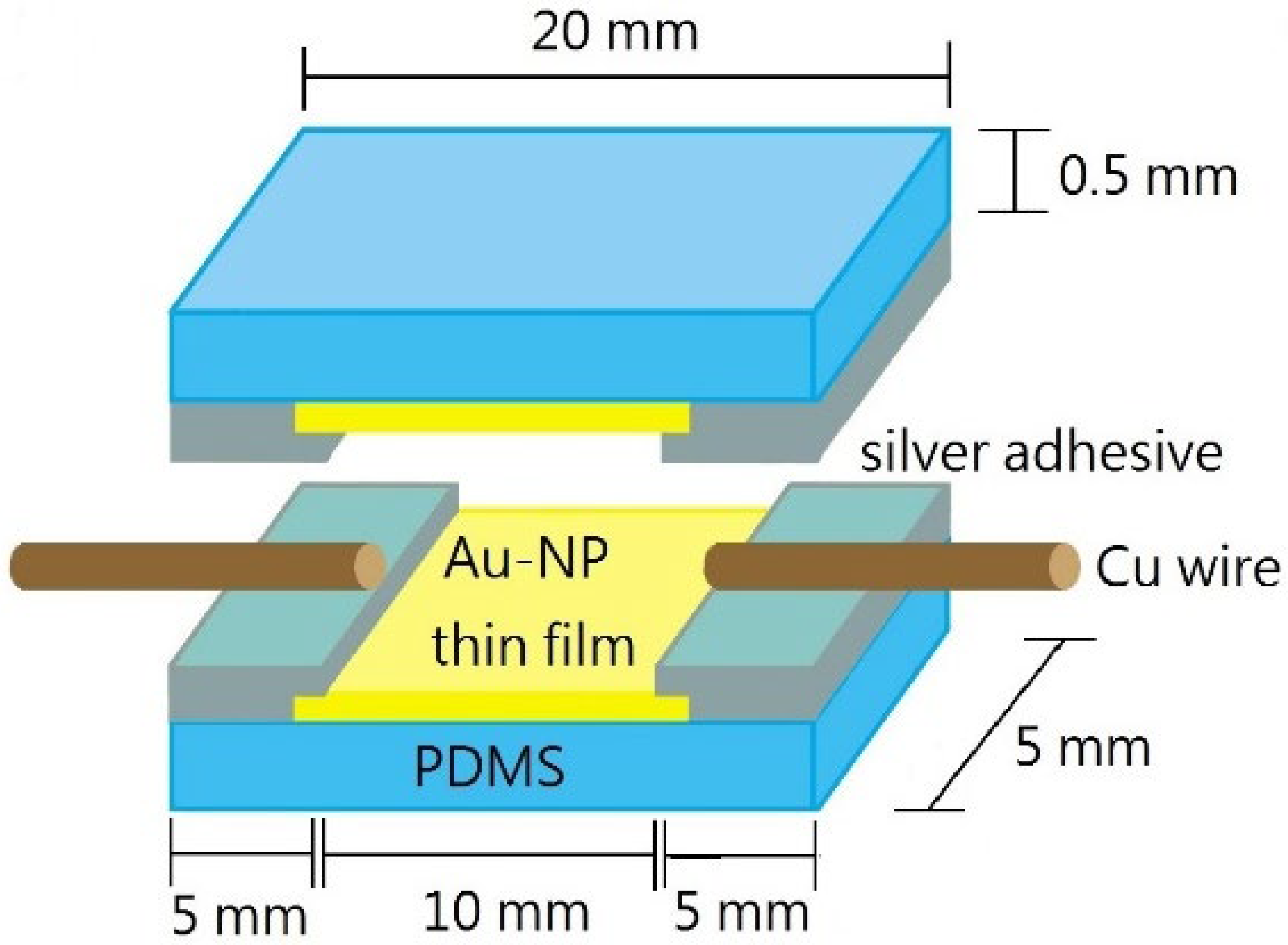
2.1. Preparation of AuNP Thin Films on PDMS
2.2. Assembly of Strain Sensors
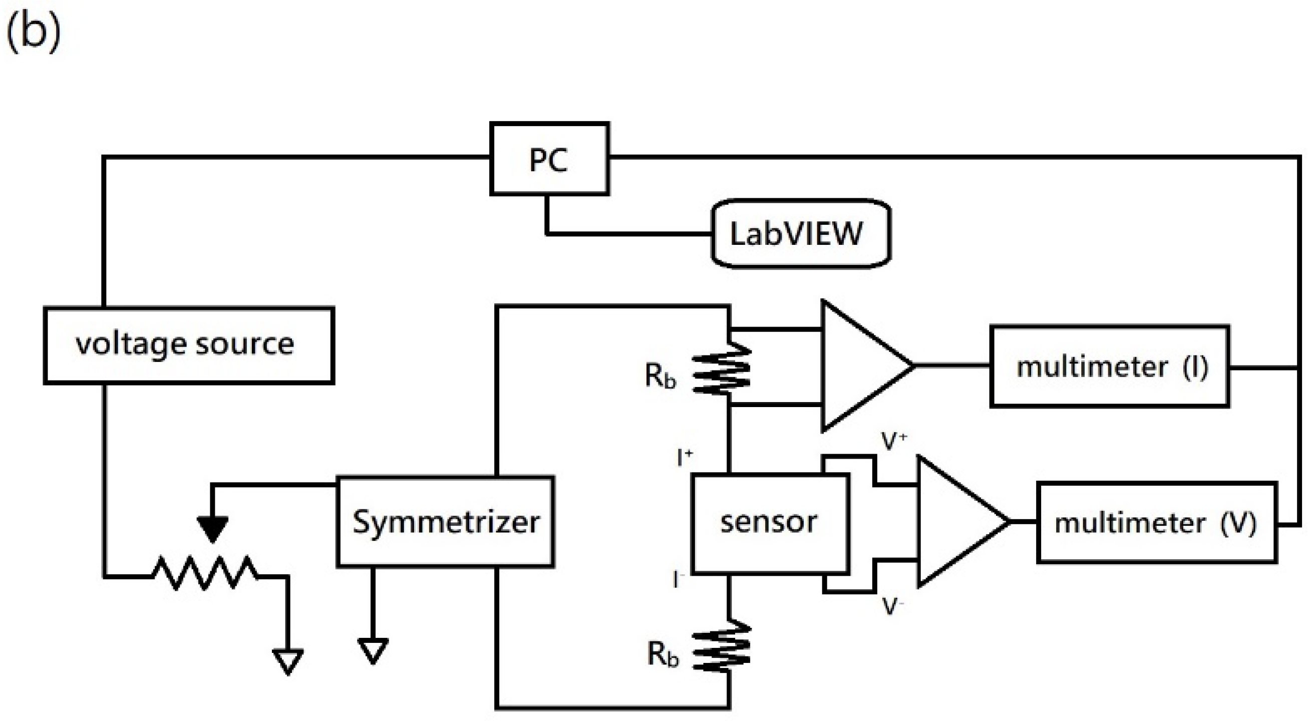
2.3. Characterization Measurement
3. Results and Discussion
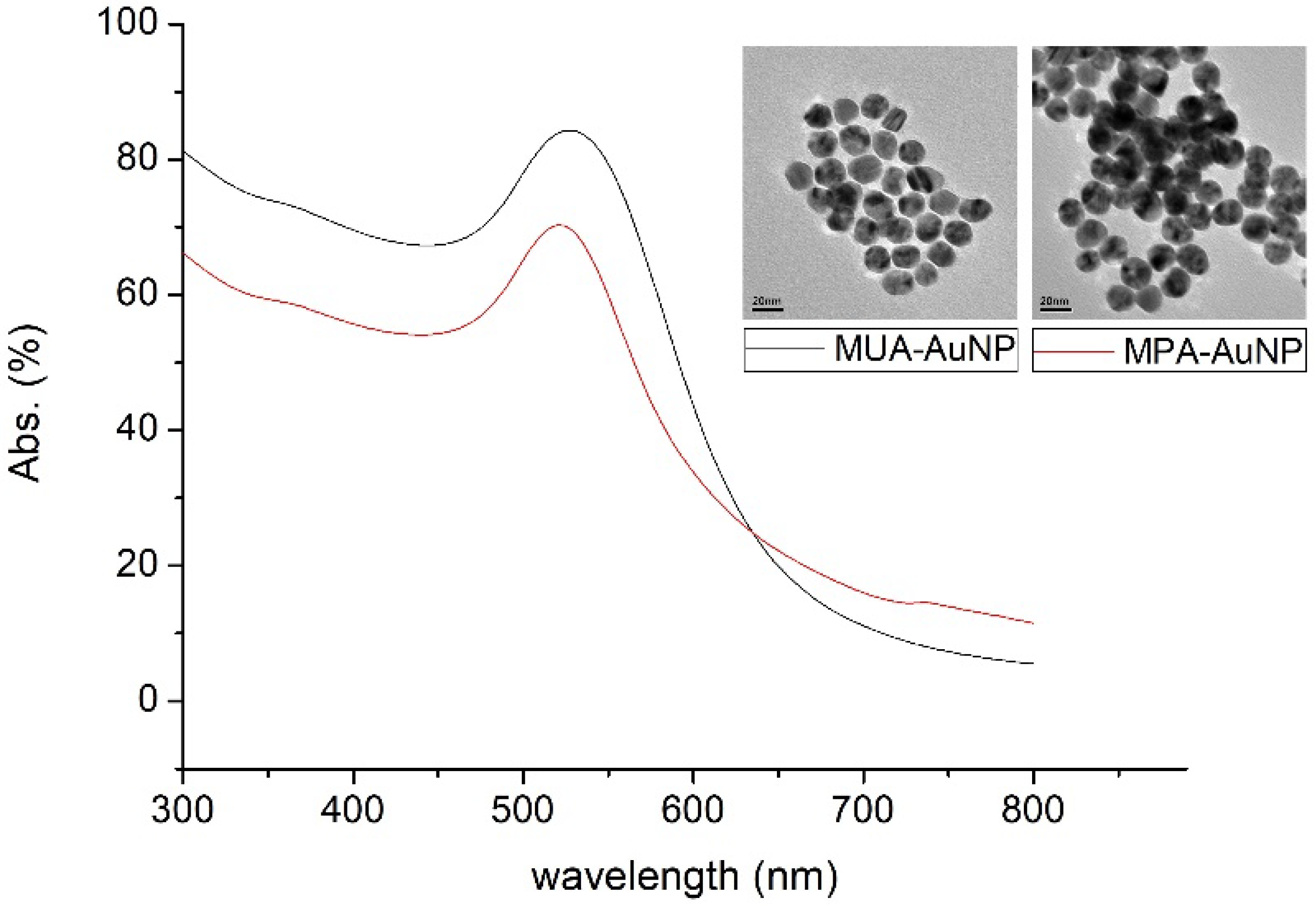
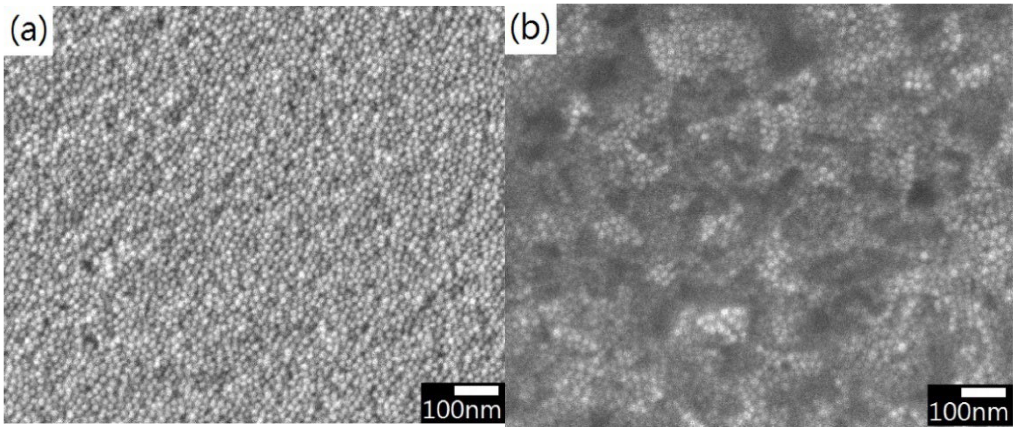
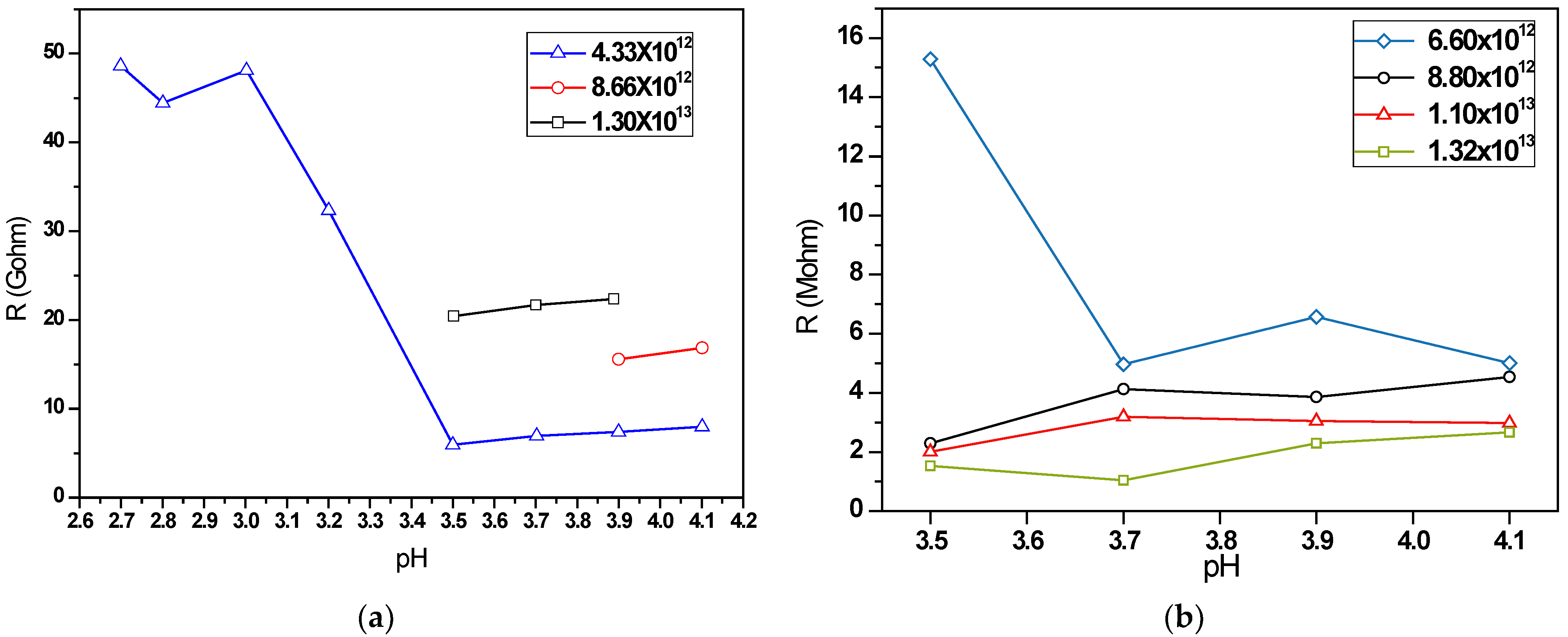
3.1. Resistance of MUA Devices and MPA Devices
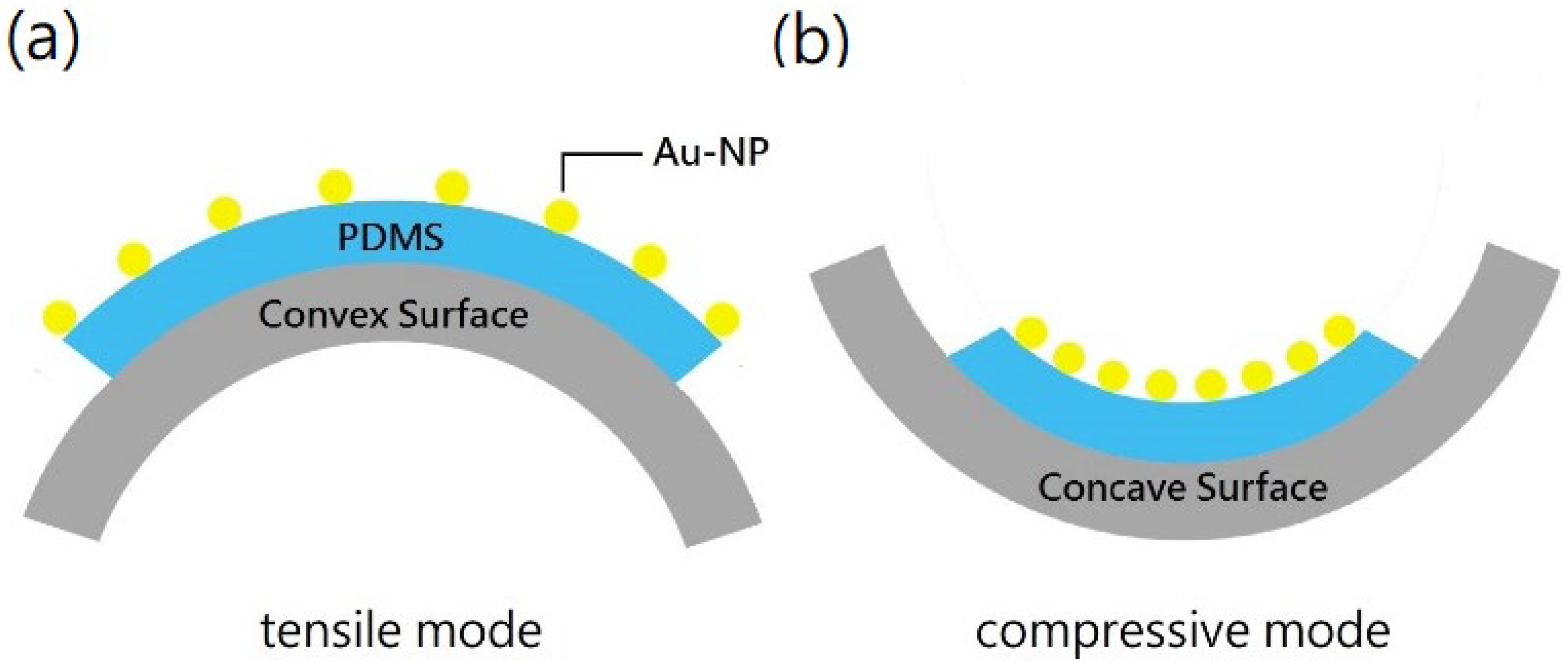
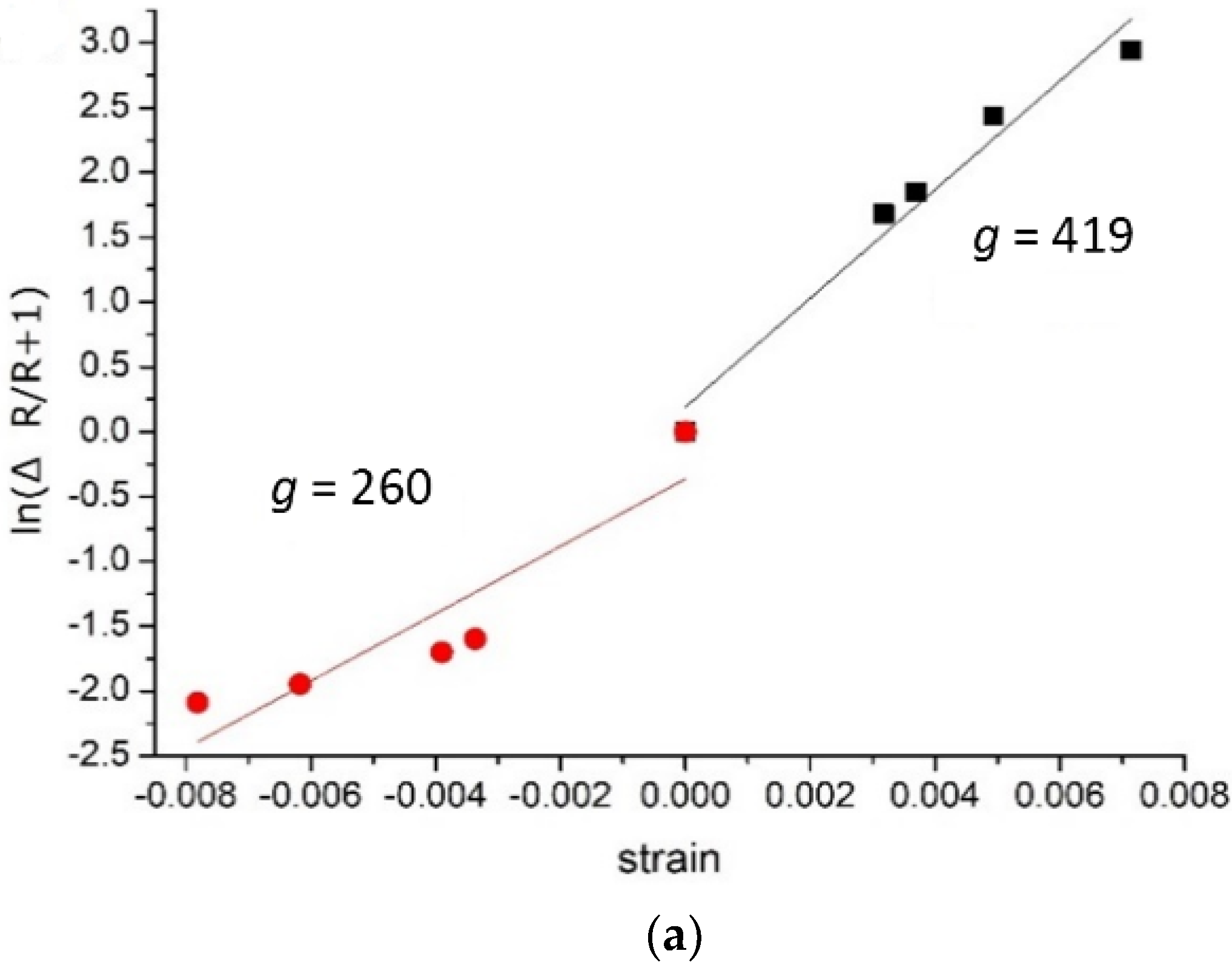
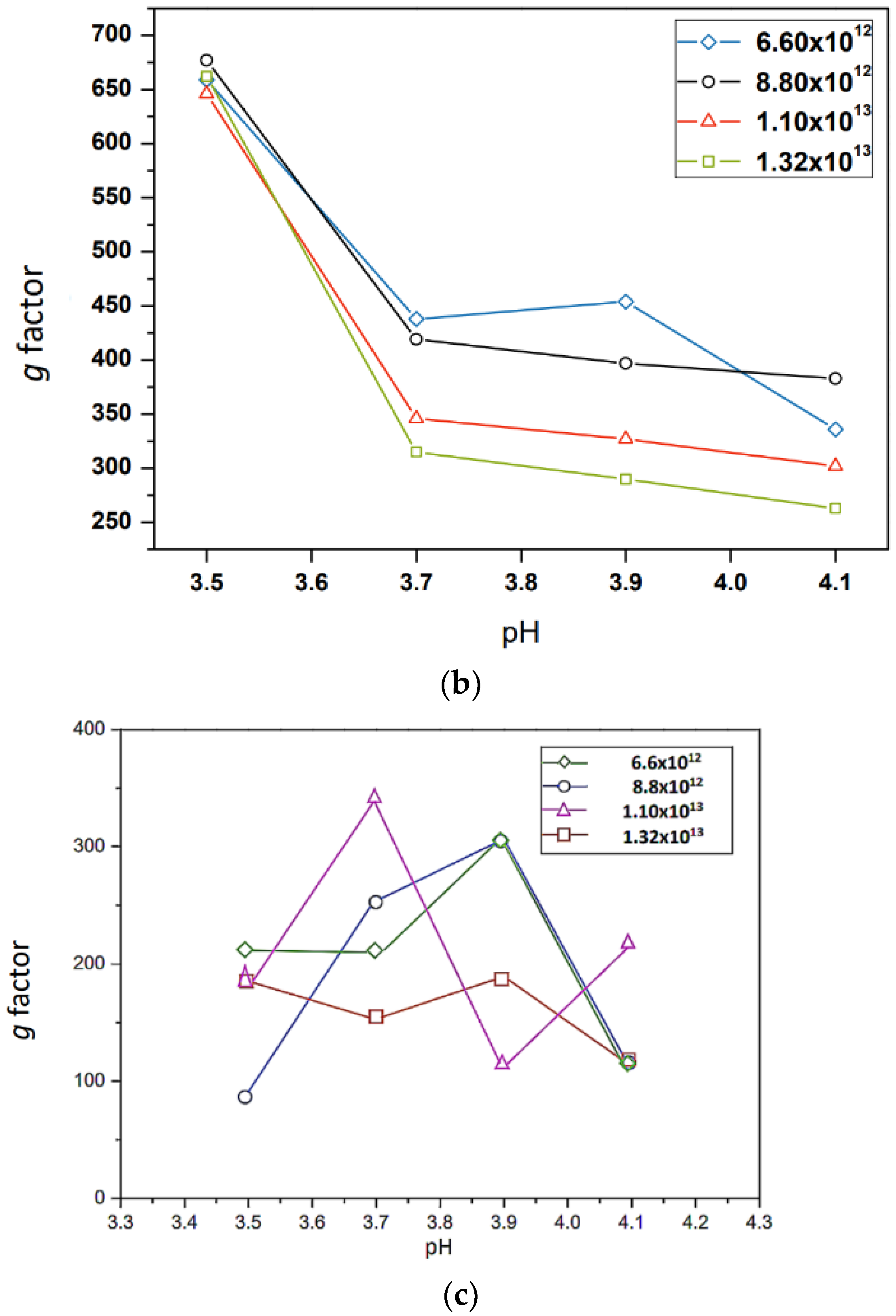
3.2. Gauge Factor of MPA Devices
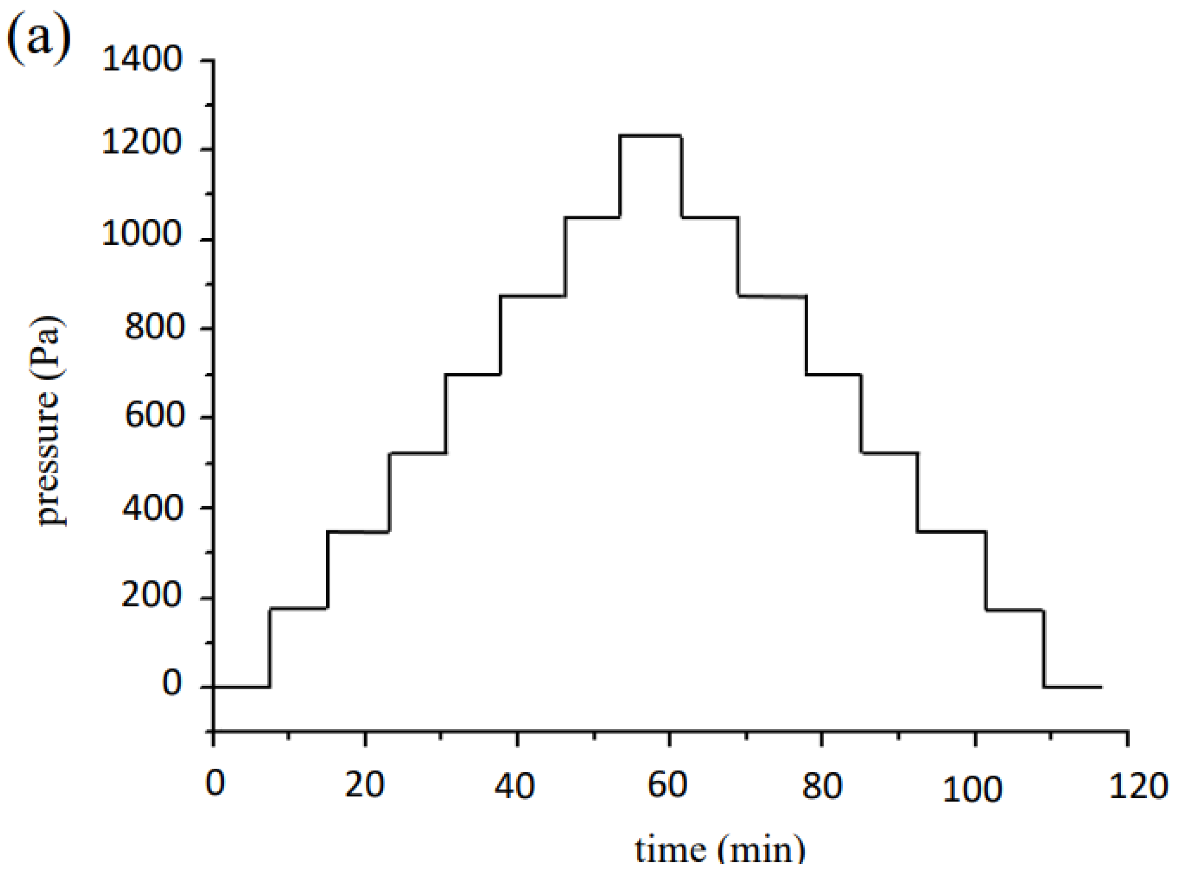
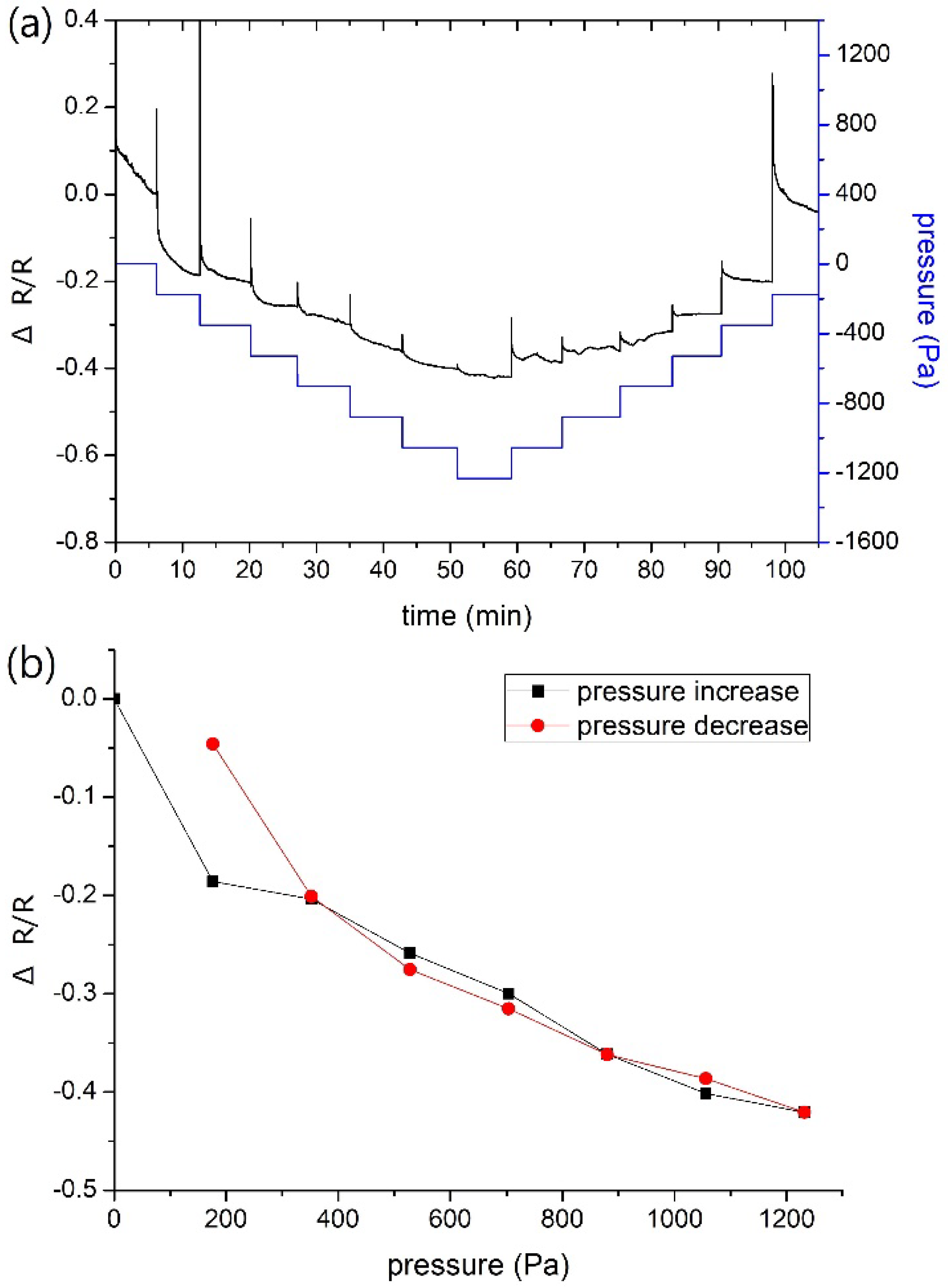
3.3. Pressure Sensitivity of MPA Devices
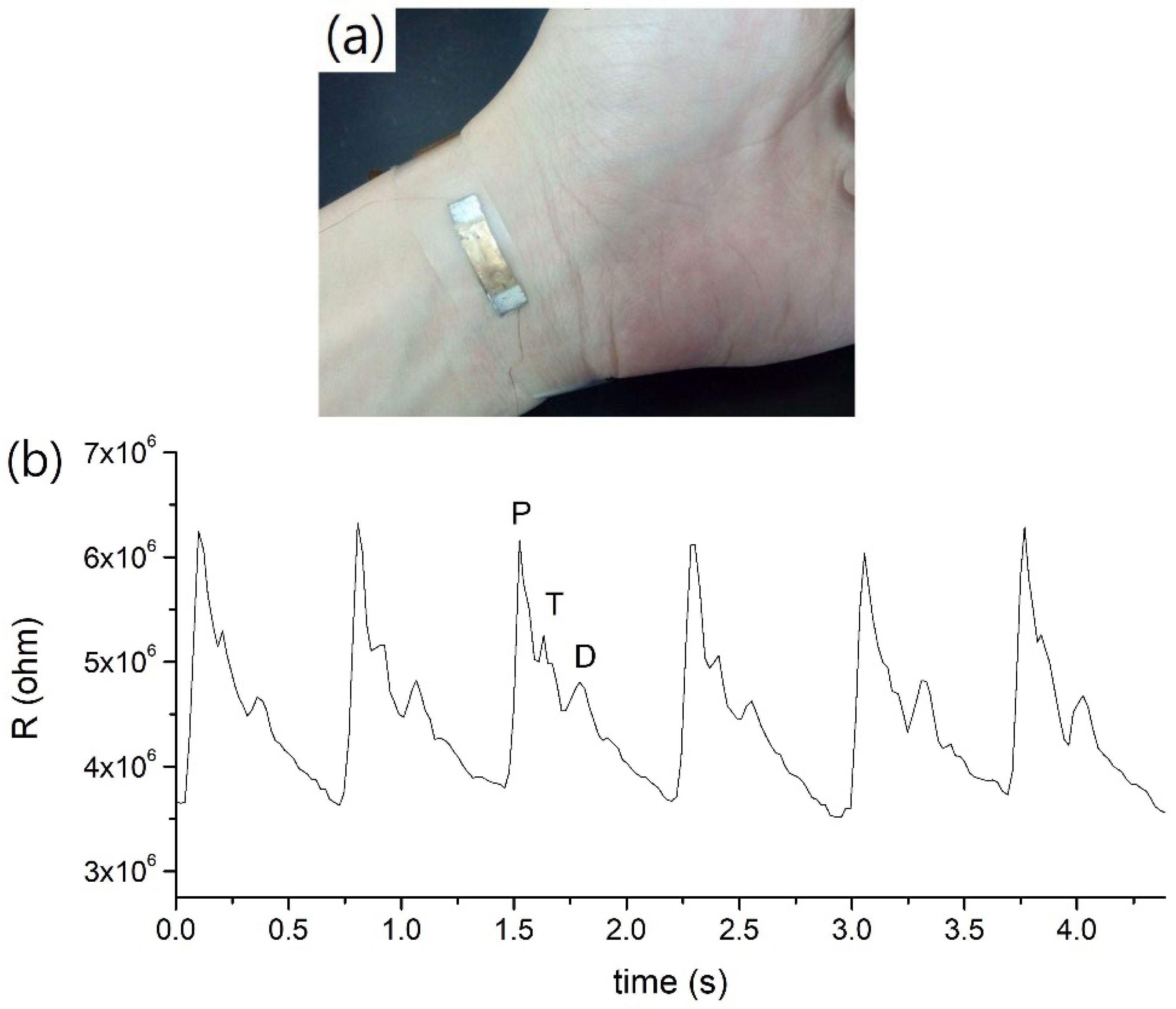
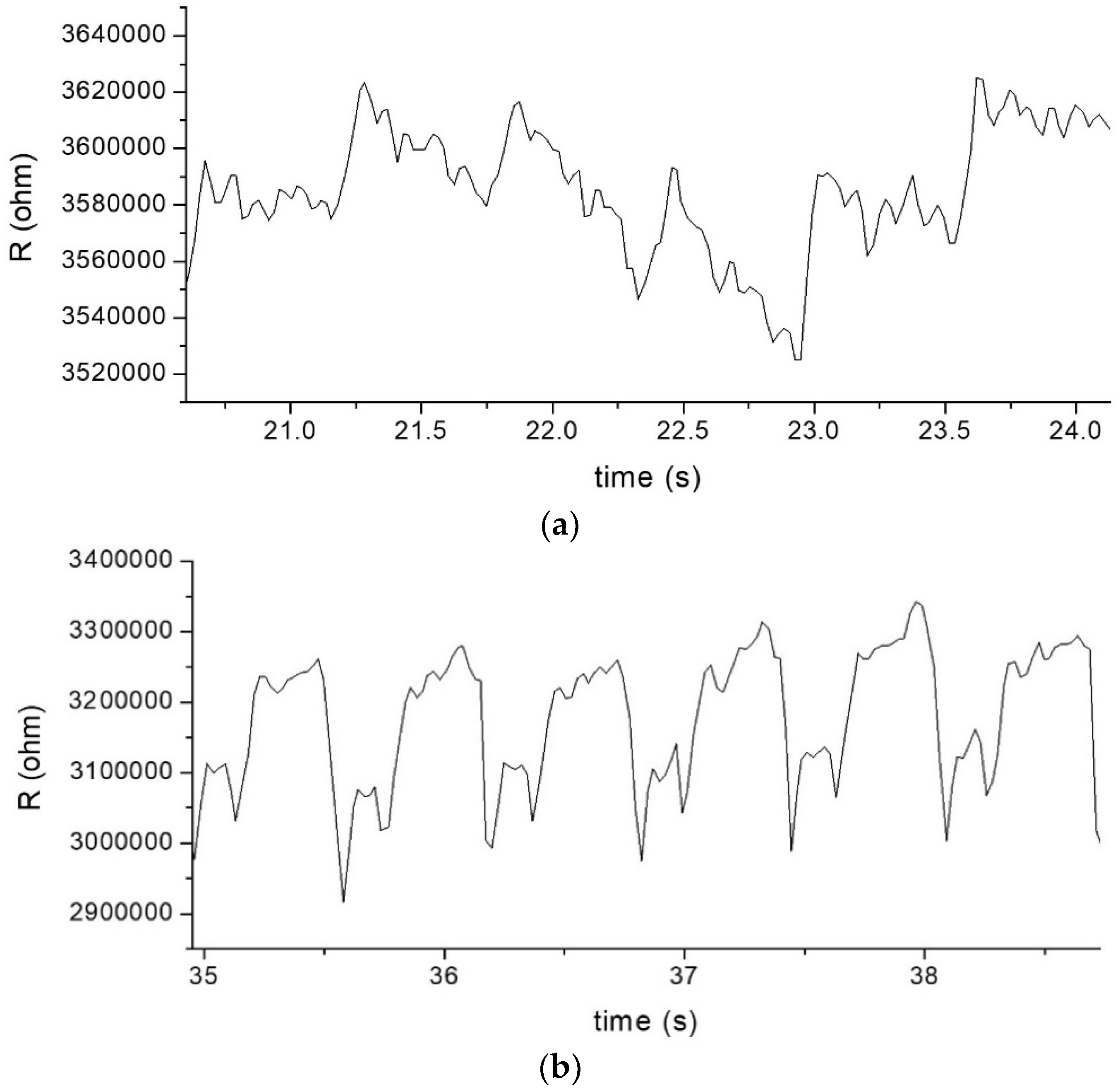
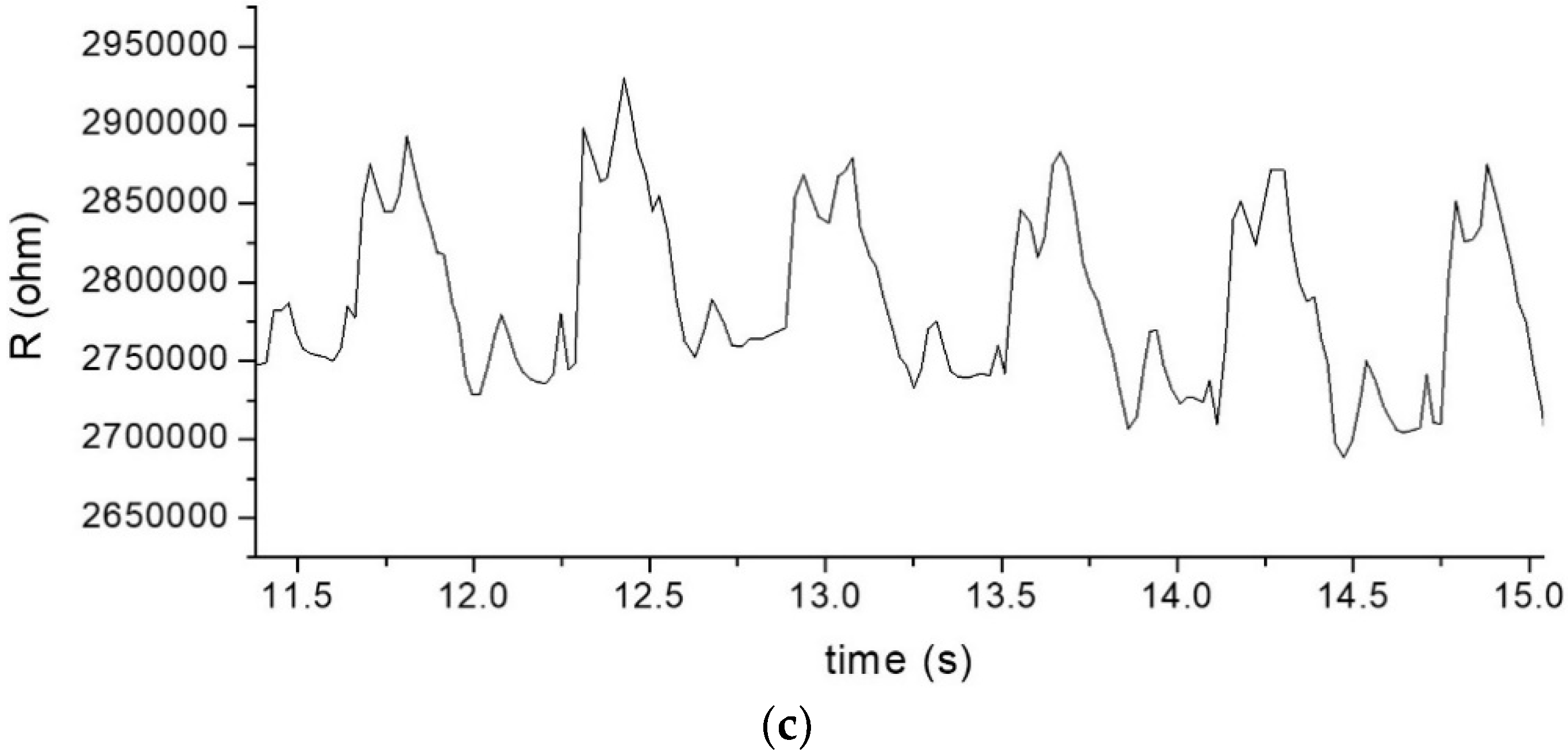
3.4. Pulse Wave Measurement with MPA Devices
4. Conclusions
Author Contributions
Funding
Data Availability Statement
Acknowledgments
Conflicts of Interest
References
- Yim, Y.-K.; Lee, C.; Lee, H.-J.; Park, K.-S. Gender and Measuring-position Differences in the Radial Pulse of Healthy Individuals. J. Acupunct. Meridian Stud. 2014, 7, 324–330. [Google Scholar] [CrossRef] [PubMed] [Green Version]
- Bridgman, P. The effect of tension on the transverse and longitudinal resistance of metals. Proc. Am. Acad. Arts Sci. 1925, 60, 423–449. [Google Scholar] [CrossRef]
- Pang, C.; Lee, G.-Y.; Kim, T.-I.; Kim, S.M.; Kim, H.N.; Ahn, S.-H.; Suh, K.-Y. A flexible and highly sensitive strain-gauge sensor using reversible interlocking of nanofibres. Nat. Mater. 2012, 11, 795–801. [Google Scholar] [CrossRef]
- Huang, Y.T.; Huang, S.C.; Hsu, C.C.; Chao, R.M.; Vu, T.K. Design and fabrication of single-walled carbon nanonet flexible strain sensors. Sensors 2012, 12, 3269. [Google Scholar] [CrossRef] [PubMed] [Green Version]
- Zheng, M.; Li, W.; Xu, M.; Xu, N.; Chen, P.; Han, M.; Xie, B. Strain sensors based on chromium nanoparticle arrays. Nanoscale 2013, 6, 3930–3933. [Google Scholar] [CrossRef]
- Chen, S.; Wei, Y.; Yuan, X.; Lin, Y.; Liu, L. A highly stretchable strain sensor based on a graphene/silver nanoparticle synergic conductive network and a sandwich structure. J. Mater. Chem. C 2016, 4, 4304–4311. [Google Scholar] [CrossRef]
- Farcau, C.; Sangeetha, N.M.; Moreira, H.; Viallet, B.; Grisolia, J.; Ciuculescu-Pradines, D.; Ressier, L. High-Sensitivity Strain Gauge Based on a Single Wire of Gold Nanoparticles Fabricated by Stop-and-Go Convective Self-Assembly. ACS Nano 2011, 5, 7137–7143. [Google Scholar] [CrossRef]
- Jiang, C.W.; Ni, I.C.; Tzeng, S.D.; Kuo, W. Nearly isotropic piezoresistive response due to charge detour conduction in na-noparticle thin films. Sci. Rep. 2015, 5, 11939. [Google Scholar] [CrossRef] [Green Version]
- Zhang, W.; Zhu, R.; Nguyen, V.; Yang, R. Highly sensitive and flexible strain sensors based on vertical zinc oxide nanowire arrays. Sens. Actuators A Phys. 2014, 205, 164–169. [Google Scholar] [CrossRef]
- Zazoum, B.; Batoo, K.M.; Khan, M.A.A. Recent Advances in Flexible Sensors and Their Applications. Sensors 2022, 22, 4653. [Google Scholar] [CrossRef]
- Segev-Bar, M.; Haick, H. Flexible Sensors Based on Nanoparticles. ACS Nano 2013, 7, 8366–8378. [Google Scholar] [CrossRef] [PubMed]
- Hayat, M.A. (Ed.) Colloidal Gold: Principles, Methods and Applications; Academic Press: San Diego, CA, USA, 1989; Volumes 1 and 2. [Google Scholar]
- Lin, S.-Y.; Tsai, Y.-T.; Chen, C.-C.; Lin, C.-M.; Chen, C.-H. Two-Step Functionalization of Neutral and Positively Charged Thiols onto Citrate-Stabilized Au Nanoparticles. J. Phys. Chem. B 2004, 108, 2134–2139. [Google Scholar] [CrossRef]
- Tao, A.R.; Huang, J.; Yang, P. Langmuir−Blodgettry of Nanocrystals and Nanowires. Acc. Chem. Res. 2008, 41, 1662–1673. [Google Scholar] [CrossRef] [PubMed]
- Lin, X.M.; Jaeger, H.M.; Sorensen, A.C.M.; Klabunde, K.J. Formation of Long-Range-Ordered Nanocrystal Superlattices on Silicon Nitride Substrates. J. Phys. Chem. B 2001, 105, 3353–3357. [Google Scholar] [CrossRef]
- Sastry, M.; Rao, M.; Ganesh, K.N. Electrostatic Assembly of Nanoparticles and Biomacromolecules. Acc. Chem. Res. 2002, 35, 847–855. [Google Scholar] [CrossRef]
- Dong, A.; Ye, X.; Chen, J.; Murray, C.B. Two-Dimensional Binary and Ternary Nanocrystal Superlattices: The Case of Monolayers and Bilayers. Nano Lett. 2011, 11, 1804–1809. [Google Scholar] [CrossRef]
- Ni, I.-C.; Yang, S.-C.; Jiang, C.-W.; Luo, C.-S.; Kuo, W.; Lin, K.-J.; Tzeng, S.-D. Formation Mechanism, Patterning, and Physical Properties of Gold-Nanoparticle Films Assembled by an Interaction-Controlled Centrifugal Method. J. Phys. Chem. C 2012, 116, 8095–8101. [Google Scholar] [CrossRef]
- Zabet-Khosousi, A.; Trudeau, P.-E.; Suganuma, Y.; Dhirani, A.-A.; Statt, B. Metal to Insulator Transition in Films of Molecularly Linked Gold Nanoparticles. Phys. Rev. Lett. 2006, 96, 156403. [Google Scholar] [CrossRef] [Green Version]
- Herrmann, J.; Müller, K.-H.; Reda, T.; Baxter, G.R.; Raguse, B.; De Groot, G.J.J.B.; Chai, R.; Roberts, M.; Wieczorek, L. Nanoparticle films as sensitive strain gauges. Appl. Phys. Lett. 2007, 91, 183105. [Google Scholar] [CrossRef]
- Yin, J.; Hu, P.; Luo, J.; Wang, L.; Cohen, M.F.; Zhong, C.-J. Molecularly Mediated Thin Film Assembly of Nanoparticles on Flexible Devices: Electrical Conductivity versus Device Strains in Different Gas/Vapor Environment. ACS Nano 2011, 5, 6516–6526. [Google Scholar] [CrossRef]
- Alvares, D.; Wieczorek, L.; Raguse, B.; Ladouceur, F.; Lovell, N. Nanoparticle films as biomimetic tactile sensors. Procedia Eng. 2011, 25, 1349. [Google Scholar] [CrossRef] [Green Version]
- Vossmeyer, T.; Stolte, C.; Ijeh, M.; Kornowski, A.; Weller, H. Networked Gold-Nanoparticle Coatings on Polyethylene: Charge Transport and Strain Sensitivity. Adv. Funct. Mater. 2008, 18, 1611–1616. [Google Scholar] [CrossRef]
- Tanner, J.L.; Mousadakos, D.; Giannakopoulos, K.; Skotadis, E.; Tsoukalas, D. High strain sensitivity controlled by the surface density of platinum nanoparticles. Nanotechnology 2012, 23, 285501. [Google Scholar] [CrossRef] [PubMed]
- Farcau, C.; Moreira, H.; Viallet, B.; Grisolia, J.; Ciuculescu-Pradines, D.; Amiens, C.; Ressier, L. Monolayered Wires of Gold Colloidal Nanoparticles for High-Sensitivity Strain Sensing. J. Phys. Chem. C 2011, 115, 14494–14499. [Google Scholar] [CrossRef]
- Huth, M. Granular metals: From electronic correlations to strain-sensing applications. J. Appl. Phys. 2010, 107, 113709. [Google Scholar] [CrossRef]
- Slowinski, K.; Chamberlain, R.V.; Miller, C.J.; Majda, M. Through-Bond and Chain-to-Chain Coupling. Two Pathways in Electron Tunneling through Liquid Alkanethiol Monolayers on Mercury Electrodes. J. Am. Chem. Soc. 1997, 119, 11910–11919. [Google Scholar] [CrossRef]
- Kang, D.; Pikhitsa, P.V.; Choi, Y.W.; Lee, C.; Shin, S.S.; Piao, L.; Park, B.; Suh, K.Y.; Kim, T.I.; Choi, M. Ultrasensitive mechanical crack-based sensor inspired by the spider sensory system. Nature 2014, 516, 222–226. [Google Scholar] [CrossRef]
- Müller, K.-H.; Herrmann, J.; Raguse, B.; Baxter, G.; Reda, T. Percolation model for electron conduction in films of metal nanoparticles linked by organic molecules. Phys. Rev. B 2002, 66, 075417. [Google Scholar] [CrossRef]
- Müller, K.-H.; Wei, G.; Raguse, B.; Myers, J. Three-dimensional percolation effect on electrical conductivity in films of metal nanoparticles linked by organic molecules. Phys. Rev. B 2003, 68, 155407. [Google Scholar] [CrossRef]
- Jheng, W.W.; Hsieh, Y.L.; Lin, Y.J.; Tzeng, S.D.; Chang, C.W.; Song, J.M.; Kuo, W. Gold nanoparticle thin film-based strain sensors for monitoring human pulse. ACS Appl. Nano Mater. 2021, 4, 1712. [Google Scholar] [CrossRef]
- Marques, F.C.; Oliveira, G.P.; Teixeira, R.A.R.; Justo, R.M.; Neves, T.B.; Andrade, G.F. Characterization of 11-mercaptoundecanoic and 3-mercaptopropionic acids adsorbed on silver by surface-enhanced Raman scattering. Vib. Spectrosc. 2018, 98, 139–144. [Google Scholar] [CrossRef]
- Phan, H.T.; Haes, A.J. What does nanoparticle stability mean? J. Phys. Chem. C 2019, 123, 16495. [Google Scholar] [CrossRef] [PubMed]
- Sadhukhan, D.; Mitra, M. R-Peak Detection Algorithm for ECG using Double Difference and RR Interval Processing. Procedia Technol. 2012, 4, 873–877. [Google Scholar] [CrossRef] [Green Version]


Publisher’s Note: MDPI stays neutral with regard to jurisdictional claims in published maps and institutional affiliations. |
© 2022 by the authors. Licensee MDPI, Basel, Switzerland. This article is an open access article distributed under the terms and conditions of the Creative Commons Attribution (CC BY) license (https://creativecommons.org/licenses/by/4.0/).
Share and Cite
Su, Y.-S.; Yang, W.-R.; Jheng, W.-W.; Kuo, W.; Tzeng, S.-D.; Yasuda, K.; Song, J.-M. Optimization of Piezoresistive Strain Sensors Based on Gold Nanoparticle Deposits on PDMS Substrates for Highly Sensitive Human Pulse Sensing. Nanomaterials 2022, 12, 2312. https://doi.org/10.3390/nano12132312
Su Y-S, Yang W-R, Jheng W-W, Kuo W, Tzeng S-D, Yasuda K, Song J-M. Optimization of Piezoresistive Strain Sensors Based on Gold Nanoparticle Deposits on PDMS Substrates for Highly Sensitive Human Pulse Sensing. Nanomaterials. 2022; 12(13):2312. https://doi.org/10.3390/nano12132312
Chicago/Turabian StyleSu, Yu-Shun, Wei-Rong Yang, Wei-Wun Jheng, Watson Kuo, Shien-Der Tzeng, Kiyokazu Yasuda, and Jenn-Ming Song. 2022. "Optimization of Piezoresistive Strain Sensors Based on Gold Nanoparticle Deposits on PDMS Substrates for Highly Sensitive Human Pulse Sensing" Nanomaterials 12, no. 13: 2312. https://doi.org/10.3390/nano12132312