

Fabrication of Black Silicon Microneedle Arrays for High Drug Loading
 , and
, and 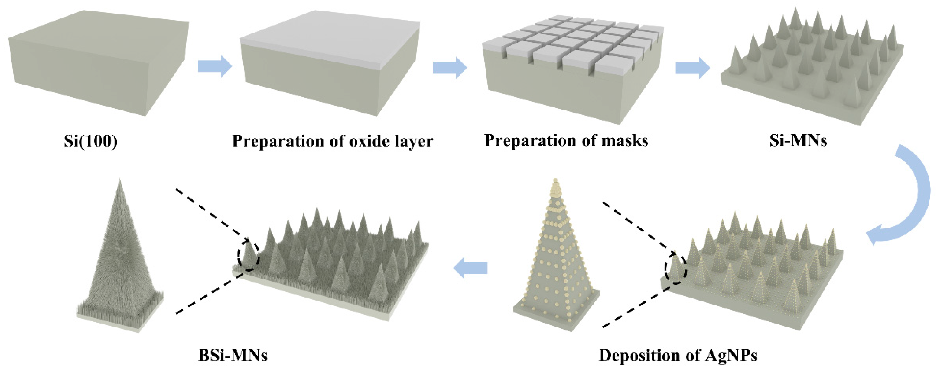
Abstract
:1. Introduction
2. Materials and Methods
2.1. Materials and Chemicals
2.2. Preparation of BSi-MN Arrays
2.3. Quantification of Drug Loading
2.4. Live/Dead Staining Experiments
2.5. Characterization
3. Results and Discussion
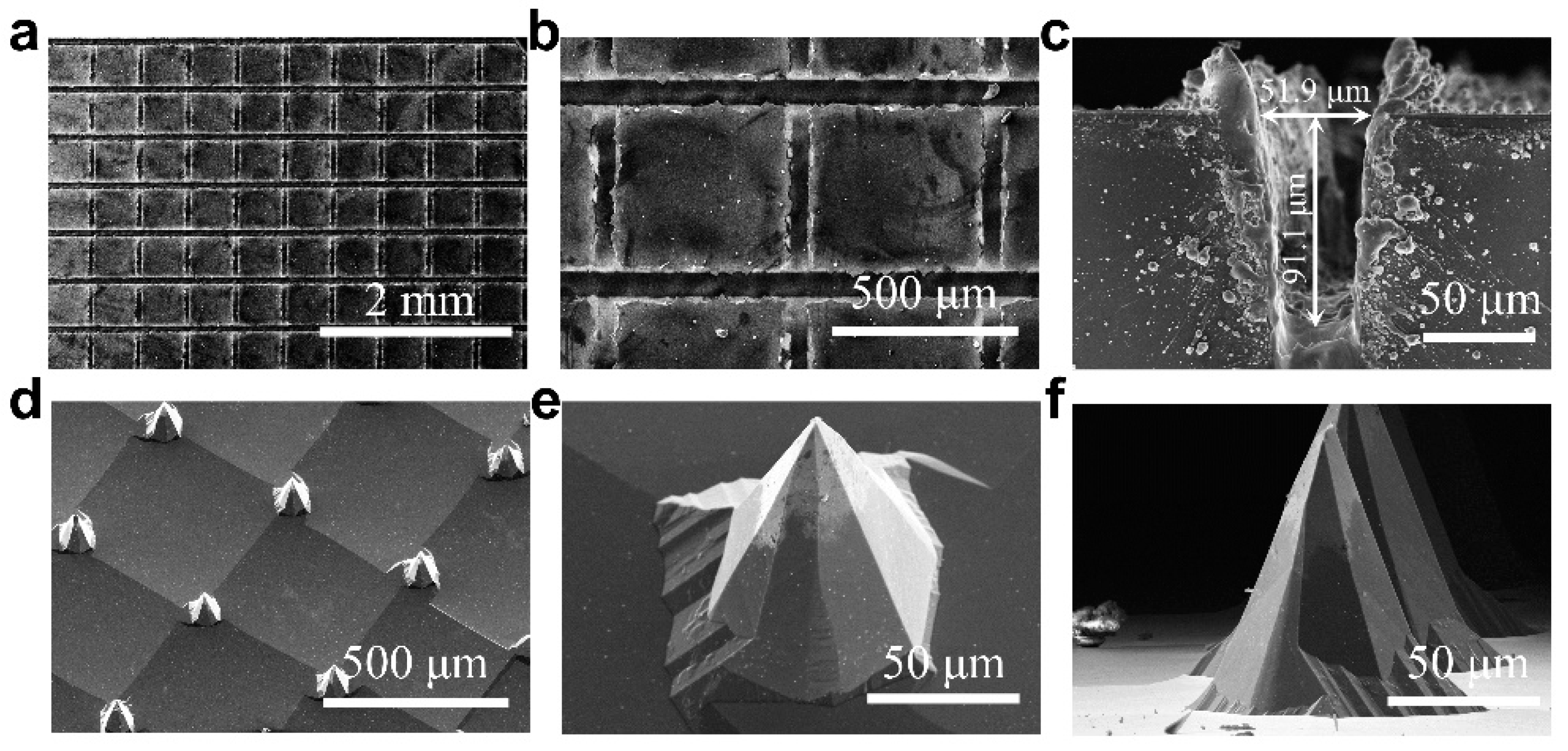
3.1. Fabrication of Si-MNs
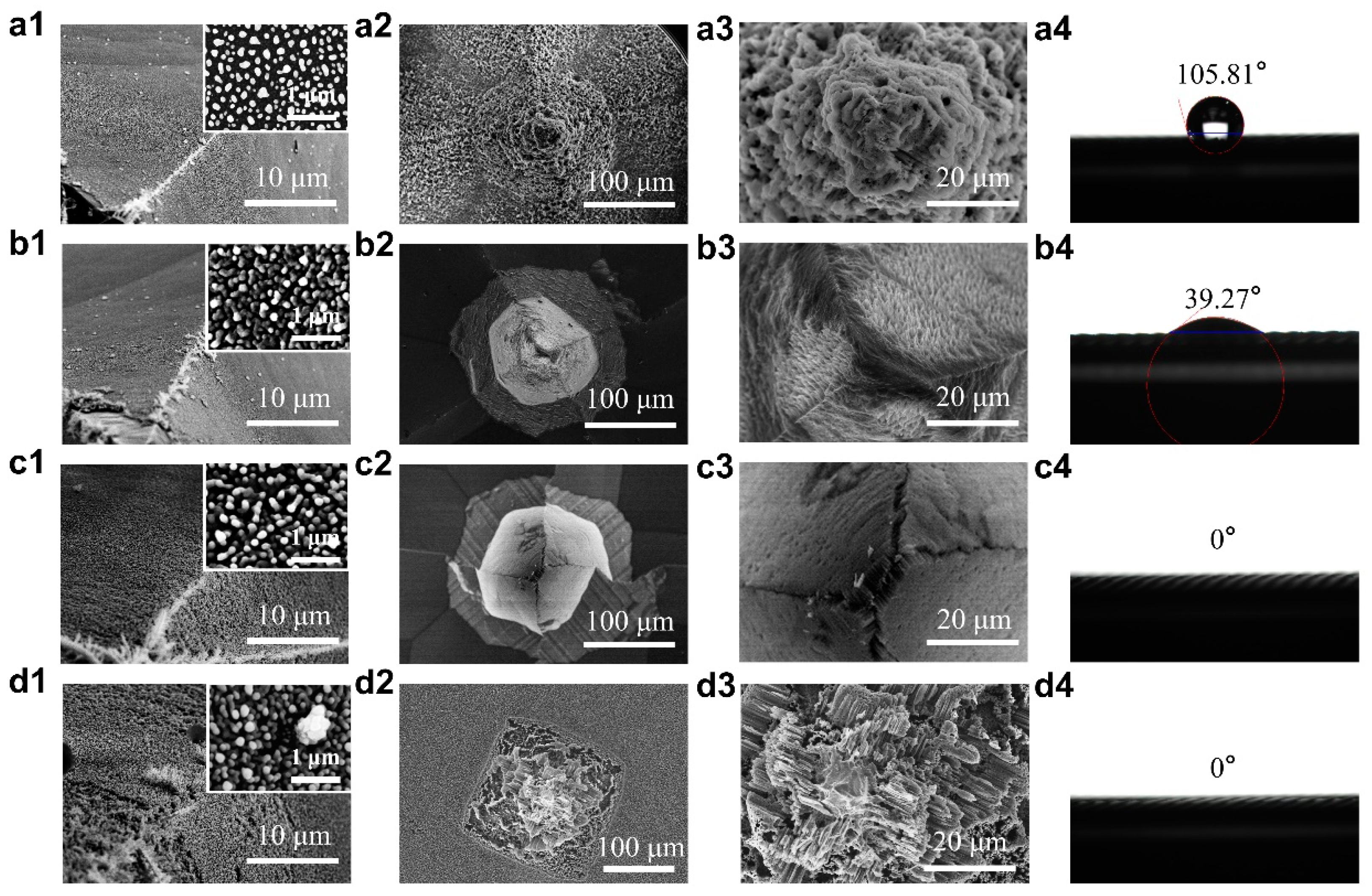
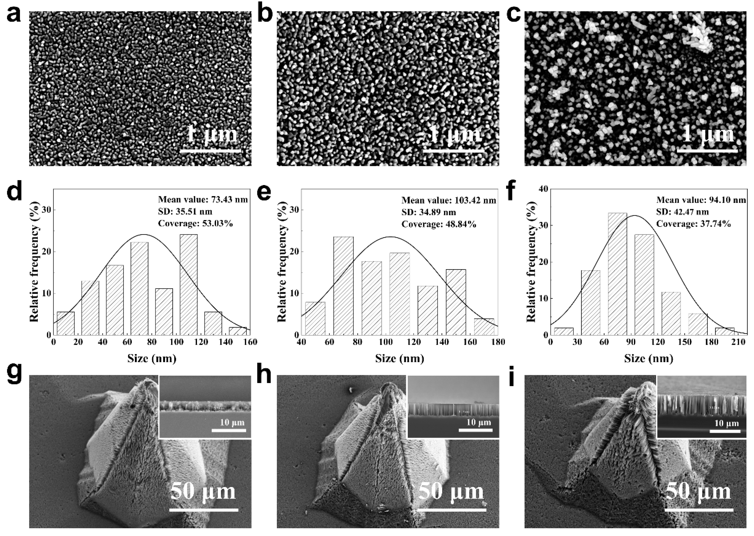
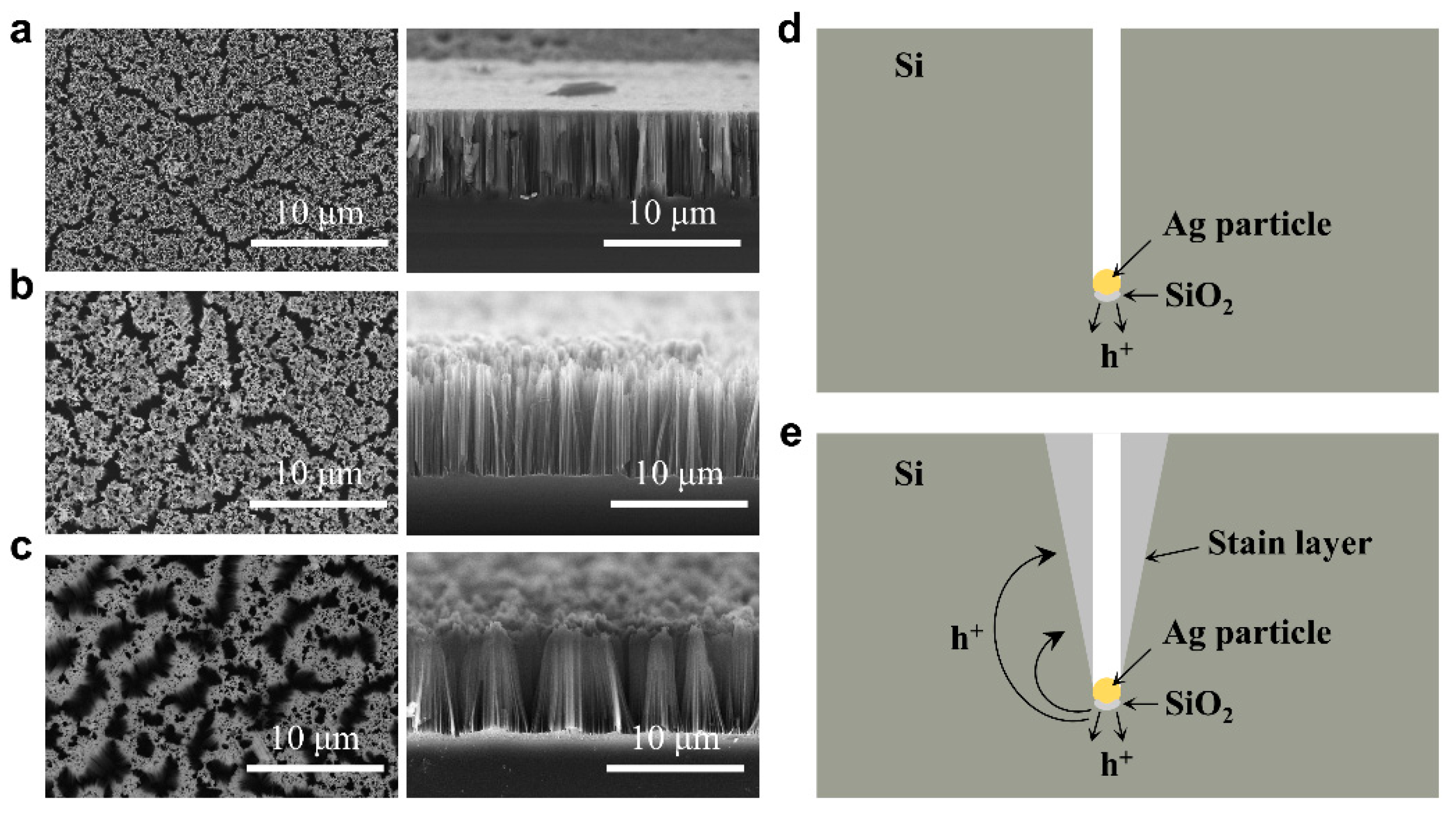
3.2. Influence of AgNO3/HF Ratio on BSi-MN Arrays
3.3. Influence of H2O2/HF Ratio on BSi-MN Arrays
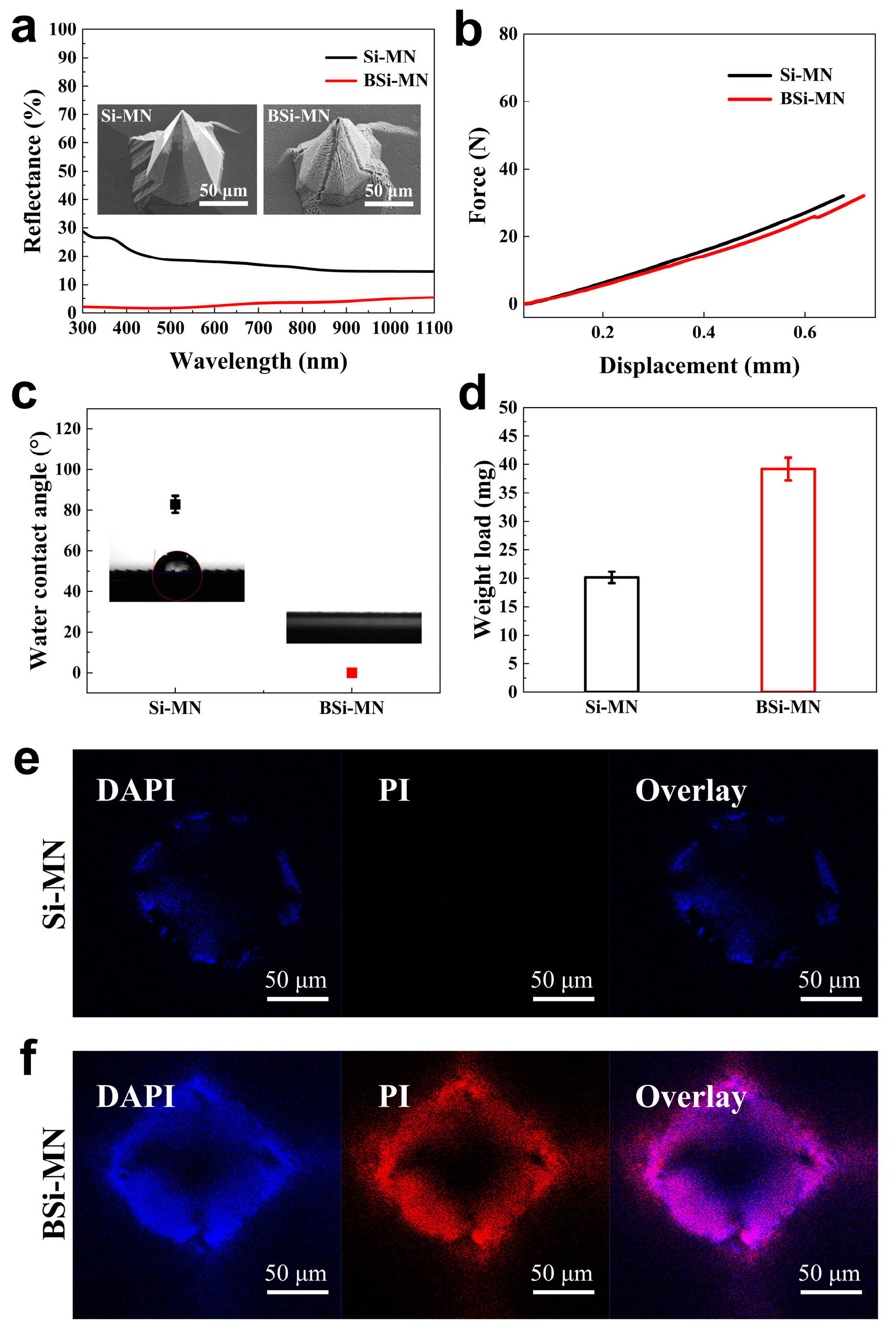
3.4. Properties of BSi-MN Arrays
3.5. Preliminary Antibacterial Experiments on BSi-MN Arrays with E.coli
4. Conclusions
Supplementary Materials
Author Contributions
Funding
Data Availability Statement
Conflicts of Interest
References
- Lee, C.; Kim, H.; Kim, S.; Lahiji, S.F.; Ha, N.Y.; Yang, H.; Kang, G.; Nguyen, H.Y.T.; Kim, Y.; Choi, M.S.; et al. Comparative Study of Two Droplet-Based Dissolving Microneedle Fabrication Methods for Skin Vaccination. Adv. Healthc. Mater. 2018, 7, e1701381. [Google Scholar] [CrossRef] [PubMed]
- Lee, C.; Kim, J.; Um, D.J.; Kim, Y.; Min, H.S.; Shin, J.; Nam, J.H.; Kang, G.; Jang, M.; Yang, H.; et al. Optimization of Layered Dissolving Microneedle for Sustained Drug Delivery Using Heat-Melted Poly(Lactic-Co-glycolic Acid). Pharmaceutics 2021, 13, 1058. [Google Scholar] [CrossRef] [PubMed]
- Lee, H.; Song, C.; Baik, S.; Kim, D.; Hyeon, T.; Kim, D.H. Device-assisted transdermal drug delivery. Adv. Drug Deliv. Rev. 2018, 127, 35–45. [Google Scholar] [CrossRef] [PubMed]
- Zhang, Y.; Yu, J.; Kahkoska, A.R.; Wang, J.; Buse, J.B.; Gu, Z. Advances in transdermal insulin delivery. Adv. Drug Deliv. Rev. 2019, 139, 51–70. [Google Scholar] [CrossRef] [PubMed]
- Kovacik, A.; Kopecna, M.; Vavrova, K. Permeation enhancers in transdermal drug delivery: Benefits and limitations. Expert Opin. Drug Deliv. 2020, 17, 145–155. [Google Scholar] [CrossRef] [PubMed]
- Ahad, A.; Raish, M.; Bin Jardan, Y.A.; Al-Mohizea, A.M.; Al-Jenoobi, F.I. Delivery of Insulin via Skin Route for the Management of Diabetes Mellitus: Approaches for Breaching the Obstacles. Pharmaceutics 2021, 13, 100. [Google Scholar] [CrossRef] [PubMed]
- Joshi, D.; Gala, R.P.; Uddin, M.N.; D’Souza, M.J. Novel ablative laser mediated transdermal immunization for microparticulate measles vaccine. Int. J. Pharm. 2021, 606, 120882. [Google Scholar] [CrossRef] [PubMed]
- Li, Y.; Yang, J.; Zheng, Y.; Ye, R.; Liu, B.; Huang, Y.; Zhou, W.; Jiang, L. Iontophoresis-driven porous microneedle array patch for active transdermal drug delivery. Acta Biomater. 2021, 121, 349–358. [Google Scholar] [CrossRef]
- Han, T.Y.; Park, K.Y.; Ahn, J.Y.; Kim, S.W.; Jung, H.J.; Kim, B.J. Facial skin barrier function recovery after microneedle transdermal delivery treatment. Dermatol. Surg. 2012, 38, 1816–1822. [Google Scholar] [CrossRef]
- Chen, S.; Miyazaki, T.; Itoh, M.; Matsumoto, H.; Moro-Oka, Y.; Tanaka, M.; Miyahara, Y.; Suganami, T.; Matsumoto, A. A Porous Reservoir-Backed Boronate Gel Microneedle for Efficient Skin Penetration and Sustained Glucose-Responsive Insulin Delivery. Gels 2022, 8, 74. [Google Scholar] [CrossRef]
- Gera, A.K.; Burra, R.K. The rise of polymeric Microneedles: Recent developments, advances, challenges, and applications with regard to Transdermal drug delivery. J. Funct. Biomater. 2022, 13, 81. [Google Scholar] [CrossRef]
- Romanyuk, A.; Wang, R.; Marin, A.; Janus, B.M.; Felner, E.I.; Xia, D.; Goez-Gazi, Y.; Alfson, K.J.; Yunus, A.S.; Toth, E.A. Skin Vaccination with Ebola Virus Glycoprotein Using a Polyphosphazene-Based Microneedle Patch Protects Mice against Lethal Challenge. J. Funct. Biomater. 2022, 14, 16. [Google Scholar] [CrossRef] [PubMed]
- Ingrole, R.S.J.; Gill, H.S. Microneedle Coating Methods: A Review with a Perspective. J. Pharmacol. Exp. Ther. 2019, 370, 555–569. [Google Scholar] [CrossRef]
- Gill, H.S.; Prausnitz, M.R. Coated microneedles for transdermal delivery. J. Control. Release 2007, 117, 227–237. [Google Scholar] [CrossRef] [Green Version]
- Chen, B.Z.; Zhang, L.Q.; Xia, Y.Y.; Zhang, X.P.; Guo, X.D. A basal-bolus insulin regimen integrated microneedle patch for intraday postprandial glucose control. Sci. Adv. 2020, 6, eaba7260. [Google Scholar] [CrossRef]
- Jin, X.; Zhu, D.D.; Chen, B.Z.; Ashfaq, M.; Guo, X.D. Insulin delivery systems combined with microneedle technology. Adv. Drug Deliv. Rev. 2018, 127, 119–137. [Google Scholar] [CrossRef] [PubMed]
- Feng, Y.H.; Zhang, X.P.; Zhao, Z.Q.; Guo, X.D. Dissipative Particle Dynamics Aided Design of Drug Delivery Systems: A Review. Mol. Pharm. 2020, 17, 1778–1799. [Google Scholar] [CrossRef] [PubMed]
- Larrañeta, E.; Lutton, R.E.M.; Woolfson, A.D.; Donnelly, R.F. Microneedle arrays as transdermal and intradermal drug delivery systems: Materials science, manufacture and commercial development. Mater. Sci. Eng. R 2016, 104, 1–32. [Google Scholar] [CrossRef] [Green Version]
- Lee, J.W.; Prausnitz, M.R. Drug delivery using microneedle patches: Not just for skin. Expert Opin. Drug Deliv. 2018, 15, 541–543. [Google Scholar] [CrossRef]
- Li, S.; Li, W.; Prausnitz, M. Individually coated microneedles for co-delivery of multiple compounds with different properties. Drug Deliv. Transl. Res. 2018, 8, 1043–1052. [Google Scholar] [CrossRef]
- DeMuth, P.C.; Li, A.V.; Abbink, P.; Liu, J.; Li, H.; Stanley, K.A.; Smith, K.M.; Lavine, C.L.; Seaman, M.S.; Kramer, J.A. Vaccine delivery with microneedle skin patches in nonhuman primates. Nat. Biotechnol. 2013, 31, 1082–1085. [Google Scholar] [CrossRef] [PubMed] [Green Version]
- Haj-Ahmad, R.; Khan, H.; Arshad, M.S.; Rasekh, M.; Hussain, A.; Walsh, S.; Li, X.; Chang, M.-W.; Ahmad, Z. Microneedle coating techniques for transdermal drug delivery. Pharmaceutics 2015, 7, 486–502. [Google Scholar] [CrossRef] [PubMed] [Green Version]
- Caudill, C.L.; Perry, J.L.; Tian, S.; Luft, J.C.; DeSimone, J.M. Spatially controlled coating of continuous liquid interface production microneedles for transdermal protein delivery. J. Control. Release 2018, 284, 122–132. [Google Scholar] [CrossRef] [PubMed]
- Liang, L.; Chen, Y.; Zhang, B.L.; Zhang, X.P.; Liu, J.L.; Shen, C.B.; Cui, Y.; Guo, X.D. Optimization of dip-coating methods for the fabrication of coated microneedles for drug delivery. J. Drug Deliv. Sci. Technol. 2020, 55, 101464. [Google Scholar] [CrossRef]
- Park, S.C.; Kim, M.J.; Baek, S.-K.; Park, J.-H.; Choi, S.-O. Spray-formed layered polymer microneedles for controlled biphasic drug delivery. Polymers 2019, 11, 369. [Google Scholar] [CrossRef] [Green Version]
- Chen, B.Z.; Yang, Y.; Wang, B.B.; Ashfaq, M.; Guo, X.D. Self-implanted tiny needles as alternative to traditional parenteral administrations for controlled transdermal drug delivery. Int. J. Pharm. 2019, 556, 338–348. [Google Scholar] [CrossRef]
- Li, Y.; Zhang, H.; Yang, R.; Laffitte, Y.; Schmill, U.; Hu, W.; Kaddoura, M.; Blondeel, E.J.M.; Cui, B. Fabrication of sharp silicon hollow microneedles by deep-reactive ion etching towards minimally invasive diagnostics. Microsyst. Nanoeng. 2019, 5, 41. [Google Scholar] [CrossRef] [Green Version]
- Dervisevic, M.; Alba, M.; Yan, L.; Senel, M.; Gengenbach, T.R.; Prieto-Simon, B.; Voelcker, N.H. Transdermal Electrochemical Monitoring of Glucose via High-Density Silicon Microneedle Array Patch. Adv. Funct. Mater. 2021, 32, 2009850. [Google Scholar] [CrossRef]
- Howells, O.; Blayney, G.J.; Gualeni, B.; Birchall, J.C.; Eng, P.F.; Ashraf, H.; Sharma, S.; Guy, O.J. Design, fabrication, and characterisation of a silicon microneedle array for transdermal therapeutic delivery using a single step wet etch process. Eur. J. Pharm. Biopharm. 2022, 171, 19–28. [Google Scholar] [CrossRef]
- Verbaan, F.; Bal, S.; Van den Berg, D.; Dijksman, J.; Van Hecke, M.; Verpoorten, H.; Van Den Berg, A.; Luttge, R.; Bouwstra, J. Improved piercing of microneedle arrays in dermatomed human skin by an impact insertion method. J. Control. Release 2008, 128, 80–88. [Google Scholar] [CrossRef]
- Mansoor, I.; Liu, Y.; Häfeli, U.; Stoeber, B. Arrays of hollow out-of-plane microneedles made by metal electrodeposition onto solvent cast conductive polymer structures. J. Micromech. Microeng. 2013, 23, 085011. [Google Scholar] [CrossRef]
- Norman, J.J.; Choi, S.-O.; Tong, N.T.; Aiyar, A.R.; Patel, S.R.; Prausnitz, M.R.; Allen, M.G. Hollow microneedles for intradermal injection fabricated by sacrificial micromolding and selective electrodeposition. Biomed. Microdevices 2013, 15, 203–210. [Google Scholar] [CrossRef] [Green Version]
- Park, J.-H.; Allen, M.G.; Prausnitz, M.R. Biodegradable polymer microneedles: Fabrication, mechanics and transdermal drug delivery. J. Control. Release 2005, 104, 51–66. [Google Scholar] [CrossRef] [PubMed]
- McAllister, D.V.; Wang, P.M.; Davis, S.P.; Park, J.-H.; Canatella, P.J.; Allen, M.G.; Prausnitz, M.R. Microfabricated needles for transdermal delivery of macromolecules and nanoparticles: Fabrication methods and transport studies. Proc. Natl. Acad. Sci. USA 2003, 100, 13755–13760. [Google Scholar] [CrossRef] [PubMed] [Green Version]
- Khanna, P.; Luongo, K.; Strom, J.A.; Bhansali, S. Sharpening of hollow silicon microneedles to reduce skin penetration force. J. Micromech. Microeng. 2010, 20, 045011. [Google Scholar] [CrossRef]
- Stoeber, B.; Liepmann, D. Arrays of hollow out-of-plane microneedles for drug delivery. J. Microelectromech. Syst. 2005, 14, 472–479. [Google Scholar] [CrossRef]
- Mukerjee, E.; Collins, S.; Isseroff, R.; Smith, R. Microneedle array for transdermal biological fluid extraction and in situ analysis. Sens. Actuators A 2004, 114, 267–275. [Google Scholar] [CrossRef]
- Ji, J.; Tay, F.E.; Miao, J. Microfabricated hollow microneedle array using ICP etcher. J. Phys. Conf. Ser. 2006, 34, 1132. [Google Scholar] [CrossRef]
- Griss, P.; Stemme, G. Side-opened out-of-plane microneedles for microfluidic transdermal liquid transfer. J. Microelectromech. Syst. 2003, 12, 296–301. [Google Scholar] [CrossRef]
- Pradeep Narayanan, S.; Raghavan, S. Solid silicon microneedles for drug delivery applications. Int. J. Adv. Manuf. Technol. 2016, 93, 407–422. [Google Scholar] [CrossRef]
- Tabassum, N.; Alba, M.; Yan, L.; Voelcker, N.H. Porous Silicon Microneedles for Enhanced Transdermal Drug Delivery. Adv. Ther. 2022, 6, 2200156. [Google Scholar] [CrossRef]
- Gardeniers, H.J.G.E.; Luttge, R.; Berenschot, E.J.W.; de Boer, M.J.; Yeshurun, S.Y.; Hefetz, M.; van’t Oever, R.; van den Berg, A. Silicon micromachined hollow microneedles for transdermal liquid transport. J. Microelectromech. Syst. 2003, 12, 855–862. [Google Scholar] [CrossRef] [Green Version]
- Zhou, L.; Zheng, H.; Liu, Z.; Wang, S.; Liu, Z.; Chen, F.; Zhang, H.; Kong, J.; Zhou, F.; Zhang, Q. Conductive Antibacterial Hemostatic Multifunctional Scaffolds Based on Ti(3)C(2)T(x) MXene Nanosheets for Promoting Multidrug-Resistant Bacteria-Infected Wound Healing. ACS Nano 2021, 15, 2468–2480. [Google Scholar] [CrossRef]
- Qi, G.; Hu, F.; Kenry; Chong, K.C.; Wu, M.; Gan, Y.H.; Liu, B. Bacterium-Templated Polymer for Self-Selective Ablation of Multidrug-Resistant Bacteria. Adv. Funct. Mater. 2020, 30, 2001338. [Google Scholar] [CrossRef]
- Chemla, M.; Homma, T.; Bertagna, V.; Erre, R.; Kubo, N.; Osaka, T. Survey of the metal nucleation processes on silicon surfaces in fluoride solutions: From dilute HF to concentrated NH4F solutions. J. Electroanal. Chem. 2003, 559, 111–123. [Google Scholar] [CrossRef]
- Li, X.; Bohn, P. Metal-assisted chemical etching in HF/H2O2 produces porous silicon. Appl. Phys. Lett. 2000, 77, 2572–2574. [Google Scholar] [CrossRef]
- Shieh, J.; You, C.; Chiu, C.; Liu, J.; Shih, P. Black-Silicon on Micropillars with Minimal Surface Area Enlargement to Enhance the Performance of Silicon Solar Cells. Nanoscale Res. Lett. 2016, 11, 489. [Google Scholar] [CrossRef] [Green Version]
- Zhong, H.; Guo, A.; Guo, G.; Li, W.; Jiang, Y. The Enhanced Light Absorptance and Device Application of Nanostructured Black Silicon Fabricated by Metal-assisted Chemical Etching. Nanoscale Res. Lett. 2016, 11, 322. [Google Scholar] [CrossRef] [Green Version]
- Chartier, C.; Bastide, S.; Lévy-Clément, C. Metal-assisted chemical etching of silicon in HF–H2O2. Electrochim. Acta 2008, 53, 5509–5516. [Google Scholar] [CrossRef]
- Linklater, D.P.; Baulin, V.A.; Juodkazis, S.; Crawford, R.J.; Stoodley, P.; Ivanova, E.P. Mechano-bactericidal actions of nanostructured surfaces. Nat. Rev. Microbiol. 2021, 19, 8–22. [Google Scholar] [CrossRef]
- Susarrey-Arce, A.; Sorzabal-Bellido, I.; Oknianska, A.; McBride, F.; Beckett, A.J.; Gardeniers, J.G.E.; Raval, R.; Tiggelaar, R.M.; Diaz Fernandez, Y.A. Bacterial viability on chemically modified silicon nanowire arrays. J. Mater. Chem. B 2016, 4, 3104–3112. [Google Scholar] [CrossRef] [Green Version]
- Linklater, D.P.; De Volder, M.; Baulin, V.A.; Werner, M.; Jessl, S.; Golozar, M.; Maggini, L.; Rubanov, S.; Hanssen, E.; Juodkazis, S.; et al. High Aspect Ratio Nanostructures Kill Bacteria via Storage and Release of Mechanical Energy. ACS Nano 2018, 12, 6657–6667. [Google Scholar] [CrossRef]
- Li, X. Bactericidal mechanism of nanopatterned surfaces. Phys. Chem. Chem. Phys. 2016, 18, 1311–1316. [Google Scholar] [CrossRef]


Disclaimer/Publisher’s Note: The statements, opinions and data contained in all publications are solely those of the individual author(s) and contributor(s) and not of MDPI and/or the editor(s). MDPI and/or the editor(s) disclaim responsibility for any injury to people or property resulting from any ideas, methods, instructions or products referred to in the content. |
© 2023 by the authors. Licensee MDPI, Basel, Switzerland. This article is an open access article distributed under the terms and conditions of the Creative Commons Attribution (CC BY) license (https://creativecommons.org/licenses/by/4.0/).
Share and Cite
Cheng, W.; Wang, X.; Zou, S.; Ni, M.; Lu, Z.; Dai, L.; Su, J.; Yang, K.; Su, X. Fabrication of Black Silicon Microneedle Arrays for High Drug Loading. J. Funct. Biomater. 2023, 14, 245. https://doi.org/10.3390/jfb14050245
Cheng W, Wang X, Zou S, Ni M, Lu Z, Dai L, Su J, Yang K, Su X. Fabrication of Black Silicon Microneedle Arrays for High Drug Loading. Journal of Functional Biomaterials. 2023; 14(5):245. https://doi.org/10.3390/jfb14050245
Chicago/Turabian StyleCheng, Wei, Xue Wang, Shuai Zou, Mengfei Ni, Zheng Lu, Longfei Dai, Jiandong Su, Kai Yang, and Xiaodong Su. 2023. "Fabrication of Black Silicon Microneedle Arrays for High Drug Loading" Journal of Functional Biomaterials 14, no. 5: 245. https://doi.org/10.3390/jfb14050245