Article

A Super-Efficient TinyML Processor for the Edge Metaverse

by
Arash Khajooei
1,
Mohammad (Behdad) Jamshidi
2,* and
Shahriar B. Shokouhi
1
1
School of Electrical Engineering, Iran University of Science and Technology, Tehran 13114-16846, Iran
2
Faculty of Electrical Engineering, University of West Bohemia, Univerzitni 2795/26, 301-00 Pilsen, Czech Republic
*
Author to whom correspondence should be addressed.
Information 2023, 14(4), 235; https://doi.org/10.3390/info14040235
Submission received: 15 March 2023 / Revised: 2 April 2023 / Accepted: 4 April 2023 / Published: 10 April 2023

Abstract

:
Although the Metaverse is becoming a popular technology in many aspects of our lives, there are some drawbacks to its implementation on clouds, including long latency, security concerns, and centralized infrastructures. Therefore, designing scalable Metaverse platforms on the edge layer can be a practical solution. Nevertheless, the realization of these edge-powered Metaverse ecosystems without high-performance intelligent edge devices is almost impossible. Neuromorphic engineering, which employs brain-inspired cognitive architectures to implement neuromorphic chips and Tiny Machine Learning (TinyML) technologies, can be an effective tool to enhance edge devices in such emerging ecosystems. Thus, a super-efficient TinyML processor to use in the edge-enabled Metaverse platforms has been designed and evaluated in this research. This processor includes a Winner-Take-All (WTA) circuit that was implemented via a simplified Leaky Integrate and Fire (LIF) neuron on an FPGA. The WTA architecture is a computational principle in a neuromorphic system inspired by the mini-column structure in the human brain. The resource consumption of the WTA architecture is reduced by employing our simplified LIF neuron, making it suitable for the proposed edge devices. The results have indicated that the proposed neuron improves the response speed to almost 39% and reduces resource consumption by 50% compared to recent works. Using our simplified neuron, up to 4200 neurons can be deployed on VIRTEX 6 devices. The maximum operating frequency of the proposed neuron and our spiking WTA is 576.319 MHz and 514.095 MHz, respectively.

1. Introduction

Tiny Machine Learning (TinyML), which is one of the most advanced technologies of Artificial Intelligence (AI), Internet of Things (IoT), and edge computing, can be employed in a wide range of embedded systems, microsystems, and intelligent communication systems [1,2,3]. This emerging technology can streamline the realization, implementation, and utilization of machine learning (ML) approaches for smartphones, gadgets, and several edge computing-based applications, whilst it seeks much less energy compared to conventional processors, microcontrollers, and computers [3,4]. Therefore, it can be an ideal candidate for applications that have limitations in consuming energy resources, such as wireless sensor networks (WSNs). Overall, this technology includes a chip as hardware and an algorithm as software, which is typically embedded in a small package. Moreover, considering their noticeable performance and extremely low power, the development of these technologies can revolutionize the infrastructures of edge-enabled Metaverse applications. Because energy considerations are one of the serious concerns against their development, these nodes are increasingly demanded and noticed in the industry [3].
On the other hand, as edge computing is growing, moving learning from the cloud to local devices has recently been followed by technology developers and active businesses in this area [5,6,7]. Not only does such an inverse change accelerate the process of learning in edge devices, but it al so enhances security and bandwidth. In other words, it improves the edge applications in the edge layer. One of the critical stages in state-of-the-art training ML models on edge devices is their resource consumption, performance, and efficiency. In this regard, this paper presents a super-efficient TinyML, which can be used for many applications in the Metaverse, especially for edge-enabled Metaverse applications [8,9,10]. Accordingly, all processes of the design, simulation, and validation of the proposed TinyML processor are taken into consideration in this paper.
FPGAs are highly flexible, reliable, and straightforward-to-design neural networks [11]. However, despite many advances in digital technology, digital platforms still deal with some challenges. One of these main challenges is the number of resources that are available on the FPGA devices. Therefore, the simplicity of a neuron model and its implementation are considered significant factors in neuromorphic circuit design. In this respect, a large number of studies have been published on the design of the spiking neuron models and Spiking Neural Networks (SNNs) on FPGAs. Cassidy et al. [11] present an array of 32 dynamical digital silicon neurons and implement the Izhikevich neuron model. Both of these implementations were limited by the number of available fast multipliers on the chip. Karimi et al. and Nouri et al. [12,13] introduce digital methods for the implementation of Wilson and FitzHugh–Nagumo neuron models, respectively. They analyze these neuron models theoretically and confirm that their proposed hardware is an appropriate model for large-scale digital implementation. Hayati et al. [14,15] implement Hindmarsh–Rose and Morris-Lecar on FPGAs. The research showed that the Hindmarsh–Rose model can mimic the desired behaviors of the neuron. Additionally, this model can be implemented on digital platforms. Furthermore, a set of piecewise linear functions have been introduced to implement the Morris-car neuron model. Zaman Farsa et al. [16] present a neuromorphic system architecture based on a modified LIF neuron model. Their proposed model provides a cost-effective model that is implemented on the VIRTEX6 device.
The advantages of digital circuits that can enhance edge devices in the edge layer motivate us to introduce a simplified LIF neuron for implementation on FPGAs. This model describes a relation between the membrane voltage of the neuron and its neuronal membrane currents. The main goal is to reduce the consumption occupied by the neuron to make it feasible for digital implementation. In addition, a floating-point-based model of the LIF neuron is implemented to be compared with the proposed simplified neuron. The results show that the resource consumption of the simplified neuron decreased dramatically, including the number of LUTs and slice registers on FPGAs. Finally, a spiking WTA circuit is implemented to evaluate the applicability of our proposed neuron in SNNs.
In summary, the most significant contributions of this research can be listed as follows:
i
Designing, implementing, and evaluating a super-efficient neuromorphic processor, including a Winner-Take-All (WTA) circuit and a simplified Leaky Integrate and Fire (LIF) neuron on FPGAs.
ii
Addressing the applicability and useability of the proposed processor as a practicable and powerful TinyML chip.
iii
Specifying the design process of the proposed TinyML chip for the edge-enabled Metaverse.
The rest of this paper is organized into the following sections. The structure of the LIF model, WTA architecture, and spike-timing-dependent plasticity (STDP) rule are reviewed in Section 2. Section 3 introduces the architecture of the proposed simplified neuron hardware and the floating-point implementation of the LIF neuron model. The architecture and design flow of a spiking WTA module are also described in Section 3. Section 4 provides the results of the evaluation of different SNN architectures using the proposed neuron model. Finally, Section 5 concludes the paper.

2. Backgrounds

Neuromorphic engineering, which is an emerging field that aims to implement the hardware of neural networks, is a reliable and applicable tool to design, evaluate, and realize TinyML [17,18]. It utilizes brain-inspired architectures and VLSI technology to implement high-performance and efficient chips for TinyML. A neuromorphic chip comprises distributed processing units (neurons) consisting of synapses that are implemented into various architectures of artificial neural networks (ANNs) and TinyML. Spiking Winner-Take-All (WTA) is a basic architecture of ANNs, which is inspired by cortical building blocks [19]. A WTA module is used to implement complex architectures such as associative memory [20,21]. The main processing element in a WTA block is a spiking neuron that receives and elicits spikes through its synapses and axons, respectively. There is a remarkable amount of literature that discusses the various spiking neuron models [22,23,24,25]. Each neuron model includes attributes such as the refractory period, spike-frequency adaption, and bursting, which are biological properties. These features allow the accurate emulation of a biological neuron, but complex circuitry is required to implement accurate neuron hardware. The Leaky Integrate and Fire (LIF) model is one of the most widely used models in neuromorphic systems [26]. This model offers low computational complexity and also mimics neurological neuron behavior. The aforementioned features make the LIF neuron model an appropriate choice to implement on digital platforms such as FPGAs.
As some concepts of the presented research are new in academia, some important definitions and technologies have been demonstrated in this section.

2.1. TinyML

TinyML is a new mode of computational intelligence, including several hardware and software technologies in an embedded chip, which is extremely efficient in the case of energy [3,4,27]. Hence, it is typically used in embedded edge platforms to improve data processing and enhance the speed, accuracy, and performance of embedded data analytics. Specifically, TinyML focuses on using deep neural network models and machine learning to develop highly efficient and resource-constrained devices that are enabled by microcontrollers [1]. Thus, it provides effective solutions for applications facing restrictions such as communication bandwidth constraints, high energy consumption, and latency.
Based on the lecture provided, there are several problems that are commonly associated with current Metaverse platforms. One potential solution to alleviate these problems is to design and develop an efficient TinyML processor that can meet the edge device requirements needed for Metaverse applications. By implementing the TinyML processor in the edge layer, it becomes possible to complete resource-intensive tasks such as rendering 3D virtual worlds and computing avatars locally, which greatly reduces latency and enhances overall performance. This would make the Metaverse more accessible to users and improve the user experience. In conclusion, the TinyML processor is a well-suited candidate to serve as an edge device for the next generation of Metaverse applications.

2.2. Edge-Based Metaverse

Edge computing and its effective services in the edge layer provide an enormous opportunity for the industry to benefit from Internet of Everything [27,28]. It opens a comprehensive approach for having reliable, low-latency, and fast services to connect a wide range of devices and people anywhere and anytime. On the other hand, this technology aims to transfer a main part of the computation from the cloud to a place near the users. The objective of this technological revolution is to enhance facilities to improve the quality of life. Furthermore, the Metaverse can be categorized as one of the most influential technologies among the new generation of Internet services [5,29].
On the one hand, at present, Metaverse architectures employ cloud-based methods for avatar physics emulation and graphics rendering computation, but this approach has its downsides. While there are simpler versions of the Metaverse available, they do not entirely capture the intended immersive and interconnected experience. For the Metaverse to become the successor to the current Internet, it will need to address several obstacles related to communication, networking, and computation. If these issues are not resolved, the Metaverse will face difficulties in matching the current Internet’s accessibility to billions of users [30]. The extended latency required for cloud access results in subpar visualization, which is not desirable. To tackle this issue, fresh approaches have been suggested lately that rely on edge computing architecture utilizing edge-enabled distributed computing techniques. This approach utilizes the computing power of edge devices to handle resource-intensive operations. The proposed architecture handles the computational cost of a Metaverse entity at the physical entity’s end-device, leading to a significant reduction in latency. The initial attempts to create the Metaverse are mainly ambitious projects that will need high-end devices to function properly. As a result, making the Metaverse accessible to everyone is a major obstacle [31].
On the other hand, in mobile edge networks, there is a way to process certain types of data where they are generated, rather than sending them to a centralized location. This is called cloud-edge-end computing architecture, and it allows for tasks such as handling high-dimensional data, rendering 3D virtual worlds, and computing avatars to be completed locally. In this way, edge computing has allowed regular IoT deployments to incorporate new services and opportunities. Essentially, edge computing involves using the processing and storage capabilities of end-devices and edge-nodes. By doing so, it reduces the dependency on the cloud by adding a new layer to the network architecture. This layer is responsible for aggregating, filtering, processing, and storing data [32].

2.3. Leaky Integrated and Fire Model

As mentioned in the introduction, The LIF model is one of the simplest spiking neuron models that is broadly used in neuromorphic systems and can be used in the edge devices in the edge layers for Metaverse applications. Therefore, the LIF model is used in this paper as the basic processing unit of the proposed TinyML chip. Although it is the simplest model, it has the fundamental features of spiking neurons including integration and firing. The following differential equation represents the LIF model:
τ m d u d t = ( u u e q ) + R I ,
  i f   u > u t h               u = 0
where u and u e q are the membrane potential and equilibrium potential, respectively. The membrane time constant is denoted by τ m = R.C, where R and C are membrane resistance and capacitance, respectively. In this model, when the membrane potential u reaches the threshold voltage u t h , the neuron elicits a spike, and its membrane potential u resets to u e q .
The main and fundamental part of the spike neural network is a spiking neuron, which is combined with synapses to implement various architectures of SNNs. In this paper, a spiking WTA architecture is considered as a case study and is reviewed in the next subsection.

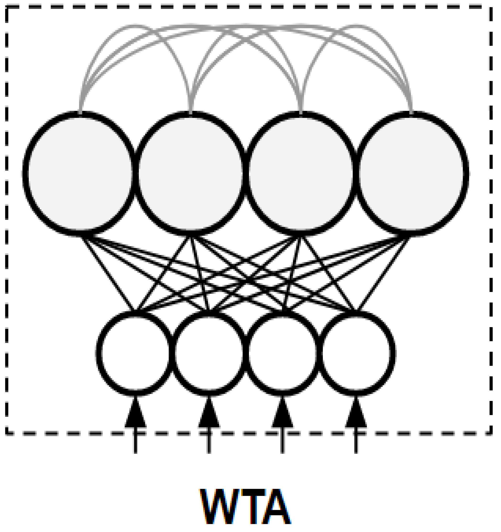
2.4. Winner-Take-All Neural Network

It is hypothesized that a Winner-Take-All (WTA) operation plays a key role in cognitive processing, which is achieved by a mini-column in the neocortex. This is a basic architecture where neurons compete with each other to become activated. Figure 1 illustrates the architecture of a spiking WTA, which consists of two layers. The input layer encodes the input patterns into spike trains, where it receives a pattern and generates a corresponding spike train for each element of the pattern [33]. The rate of each spike train is proportional to the element’s value. Following that, the spike trains are applied to the output neurons through the synaptic connections. One particular output neuron, which is called the winner neuron, is stimulated more than other neurons. Consequently, the winner elicits spikes that reset the membrane potential of the other neurons through the lateral inhibitory connection [34]. Afterward, new competition starts, and this procedure remains until the removal of the input pattern. The final winner neuron generates the spike train with the highest firing rate compared to other neurons in the WTA neural network Each output neuron is assigned to a pattern (class), and when the corresponding pattern is applied to the WTA, this output is activated [35]. The assignment of a pattern to an output neuron requires synaptic weight modification through a learning rule, which is the subject of the next subsection [36].

2.5. STDP Rule

Spike timing-dependent plasticity (STDP) is a phenomenon in which the time of spike occurrence affects the magnitude of synaptic strength. The STDP rule is used in the training phase of spiking neural networks and spiking WTA [37,38,39]. The STDP rule is the temporal form of the Hebbian rule, where Δw shows the differences in spike time between pre- and postsynaptic spikes in the neurons [40]. In a given synapse, if a presynaptic spike occurs before the postsynaptic spike, the synaptic weight will be increased. Vice versa, if the presynaptic spike appears after the postsynaptic spike, this leads to a decrease in the synaptic weight. The principal model of the STDP rule is determined by:
Δ w = { A + e Δ t / τ + , i f   Δ t > 0 A e Δ t / τ , i f   Δ t < 0 ,
The Δt in (2) equation is the time differences between presynaptic and postsynaptic spikes (Δt = tposttpre). The A+ and A parameters are the maximum and minimum values of Δw respectively, and τ+, τ are constant values.
In this section, three basic concepts were reviewed that are used in the following sections. The LIF model is simplified to be implemented on FPGAs and is used to implement a WTA architecture. The STDP rule is utilized to train the WTA, as well.

3. Implementation Method

In this section, a simplified neuron is introduced and utilized to implement a WTA architecture on the proposed TinyML chip for the edge-empowered Metaverse platforms. First, the equation of the LIF neuron model is described in a discrete form. Then, the required bits for the variable of the membrane potential u are calculated. The maximum required bit length allows us to avoid using extra hardware resources. Afterward, the implementation method of the simplified LIF neuron on FPGAs is presented, which utilizes some techniques to reduce resource consumption. Finally, the procedure of implementing a WTA SNN architecture using the simplified neuron is discussed.

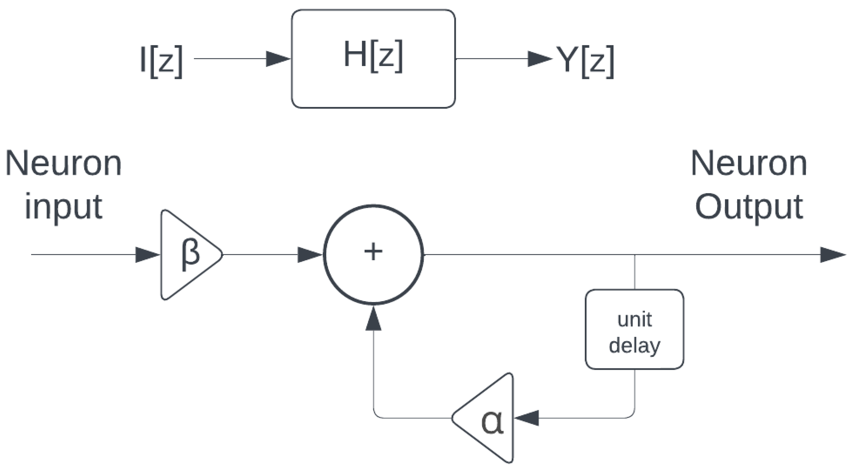
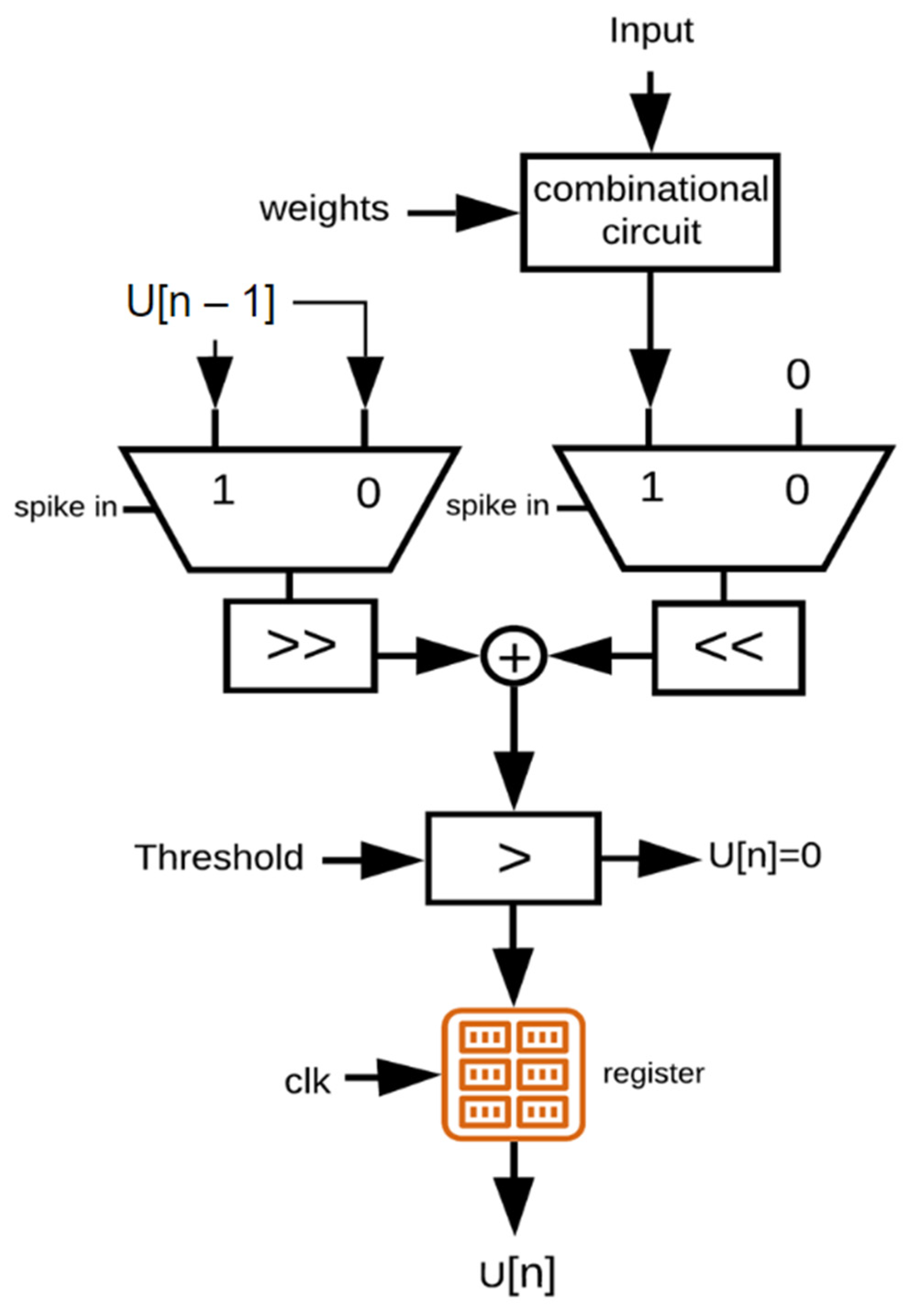
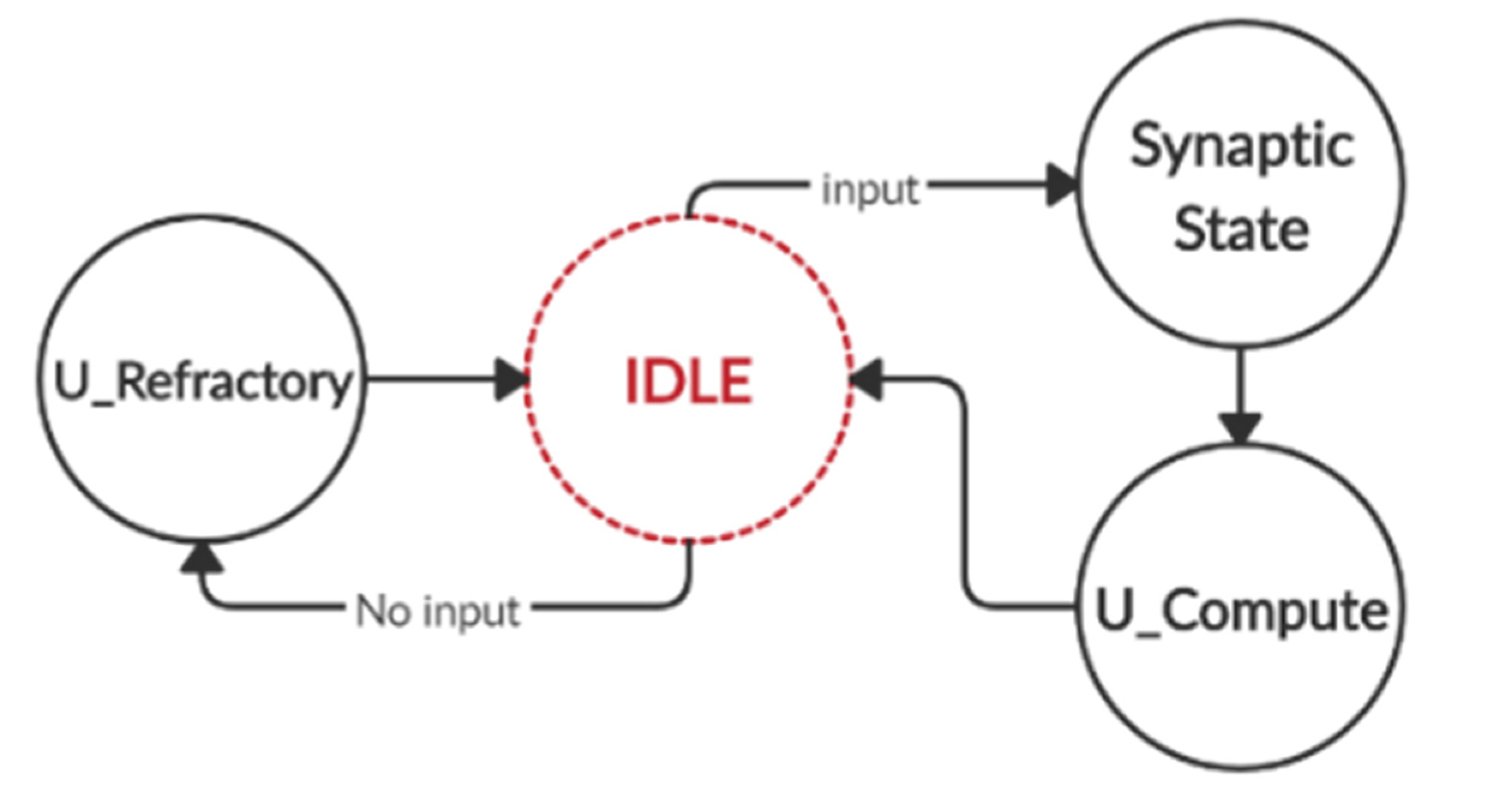
3.1. Discrete Model of an LIF Neuron

The first step of implementation of the LIF neuron on FPGAs is to discretize the analog model. The analog model described by (1) is written in a discrete form using the Euler method [12]:
u [ n ] = ( τ m τ m + 1 ) u [ n 1 ] + R τ m + 1 × I [ n ] ,
The I[n] represents the input signal of the neuron. Let us assume ( τ m τ m + 1 ) = α , and R τ m + 1 = β . Equation (3) can be written as a difference equation:
u [ n ] = α u [ n 1 ] + β Ι [ n ] ,
where | α | 1 .
In (4), α depends on τ m . Moreover, the term 𝛽 represents the amplitude of the input, which is connected to the neuron through presynaptic connections. The frequency-domain representation of (4) is obtained by using the z-transform technique:
If   I [ n ] = δ [ n ]
then
H [ z ] = β 1 α z 1
Figure 2 shows the equivalent block diagram of (4). The impulse response function of the LIF neuron system is H[z]. Now let us obtain h[n]:
H [ z ] = β 1 α z 1 z h [ n ] = β α n u [ n ]
Let us assume that the impulse train is the input of the system, which is shown by x[n]:
x [ n ] = k = 0 + δ [ n k N ]
The output of an LTI system is the convolution of the input signal and impulse response of the system. The result is shown in (9). By applying the geometric series formula:
y [ n ] = β α n u [ n ] k = 0 + δ [ n K N ] = β ( α n α N ) 1 α N
y ( + ) = β 1 α N
where the β 1 α N ratio determines the maximum value of u[n] regarding the impulse train. The parameter of N shows the period between two individual discrete pulses in the impulse train. By selecting the optimal numbers for α and β variables, the maximum output has been determined. Therefore, this equation can be used to specify the optimal number of bits that are needed for the potential register u[n].

3.2. Simplified LIF Neuron

To reduce resource consumption on the FPGA, a simplified implementation of LIF neurons is presented here. Figure 3 shows the data flow graph for the simplified LIF neuron model. The first block is a combinational circuit to multiply the neuron’s inputs with binary synaptic weights. This block consists of parallel AND logic gates to implement binary multiplication (Figure 4). The length of the input patterns determines the size of the combinational circuits, i.e., the number of the AND gates.
The outputs of the AND gates are received by the neuron to compute the membrane potential of the neuron. When there is a spike at the input, the right multiplexer and shifter increase the membrane potential value. On the other hand, the left multiplexer and shifter are used to decrease the membrane potential in the absence of input spikes. The following blocks perform multiplication and division using summation and arithmetic shifts. For binary numbers, arithmetic right shifts are equivalent to division by a positive power of two. Similarly, arithmetic left shifts are equivalent to multiplication by a positive power of two. From the hardware implementation aspect, a shifter is more efficient than a divider or multiplier circuit. Therefore, division and multiplication operations can be optimized by using arithmetic shifts. For these calculations, 32-bit fixed-point numbers are used. Finally, the value of the membrane potential is produced and compared with the threshold value. In case the value of membrane potential is higher than the threshold, a spike is generated at the output. It is worth mentioning that the length of the membrane potential is calculated using (9).
To clarify the operation of the simplified LIF neuron, the finite state machine (FSM) is depicted as a graph in Figure 5. In this diagram, nodes represent system states, and the arrows denote possible transitions between states. There are four main states that are utilized to calculate the membrane potential of the neuron. The idle state is the initial state of the system.
In the idle state, the neuron is checked for the presence of the input. Two possible scenarios happen in this state. One scenario leads to the Synaptic_in state, which is used when an input is applied. The second scenario is the U_Refractory state, which operates in the absence of the input. The neuron discharge mechanism takes place through the U_Refractory state. Finally, the last state is U_compute, and it is responsible for calculating the neuron membrane potential value.

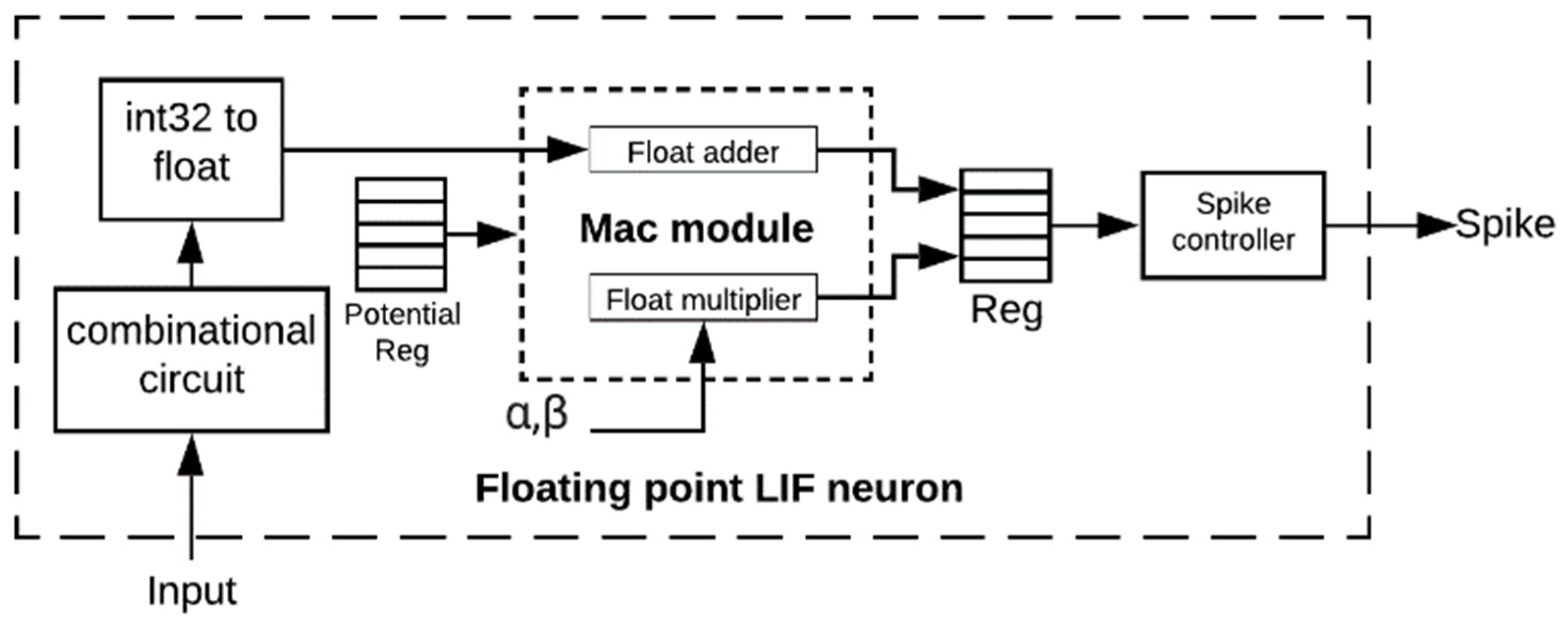
3.3. Floating-Point LIF Neuron

The second implementation, which is represented here, is the floating-point implementation of the LIF neuron. This model is used to compare with the simplified LIF neuron in terms of its performance and functionality. Figure 6 shows the architecture of the floating-point neuron. In the first stage, the combinational circuit (a set of parallel AND gates) is similar to the circuit of the simplified LIF. The second module converts the weighted inputs to floating-point numbers. The output of this unit is utilized to calculate the neuron membrane potential.
A potential register is used to sustain the current value of the membrane potential. The next module is a multiplier-accumulator unit (MAC). Another set of registers is responsible for maintaining the output of the MAC module. As shown in Figure 6, the MAC unit includes two submodules, which are adder and multiplier modules, respectively. The implementation of this unit is based on IEEE 754 floating-point algorithms [31]. Therefore, the IEEE 754 standard is used to perform this model’s floating-point operations [31]. Finally, the spike controller is used to generate spikes and reset the membrane potential to its initial value.

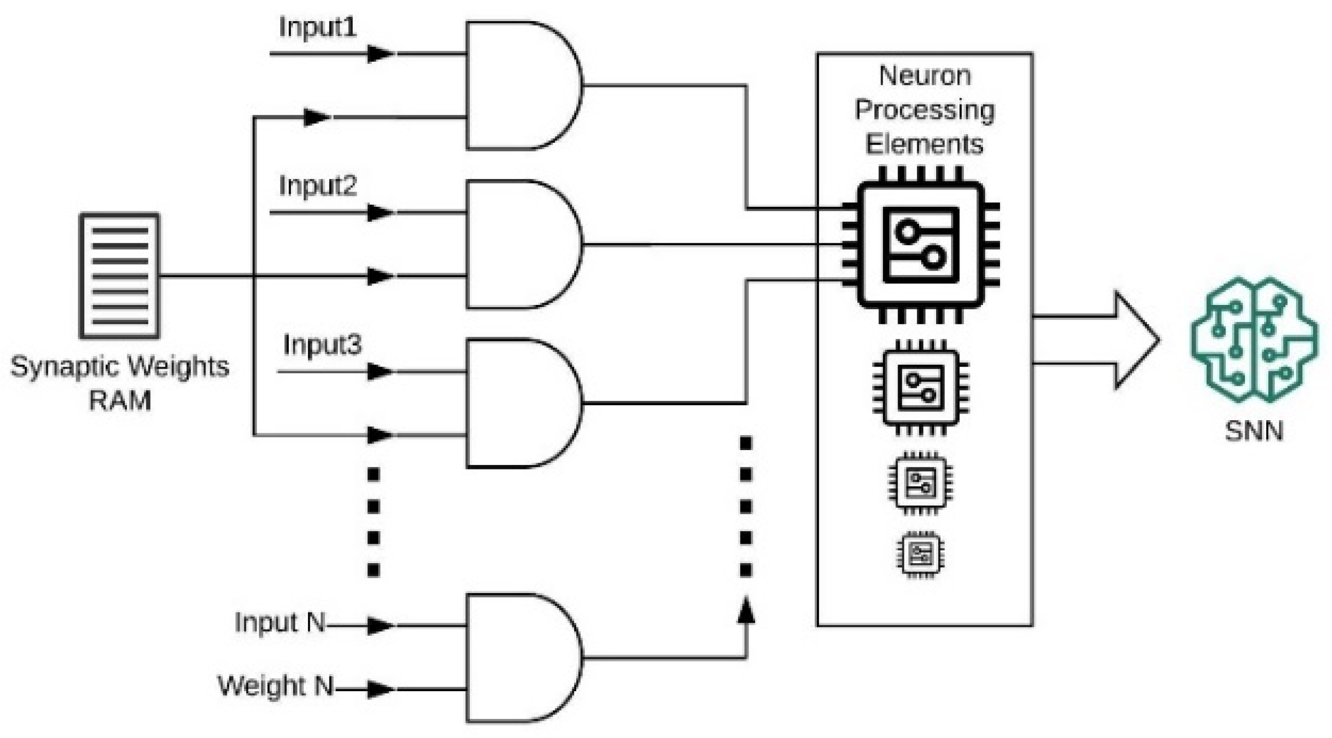
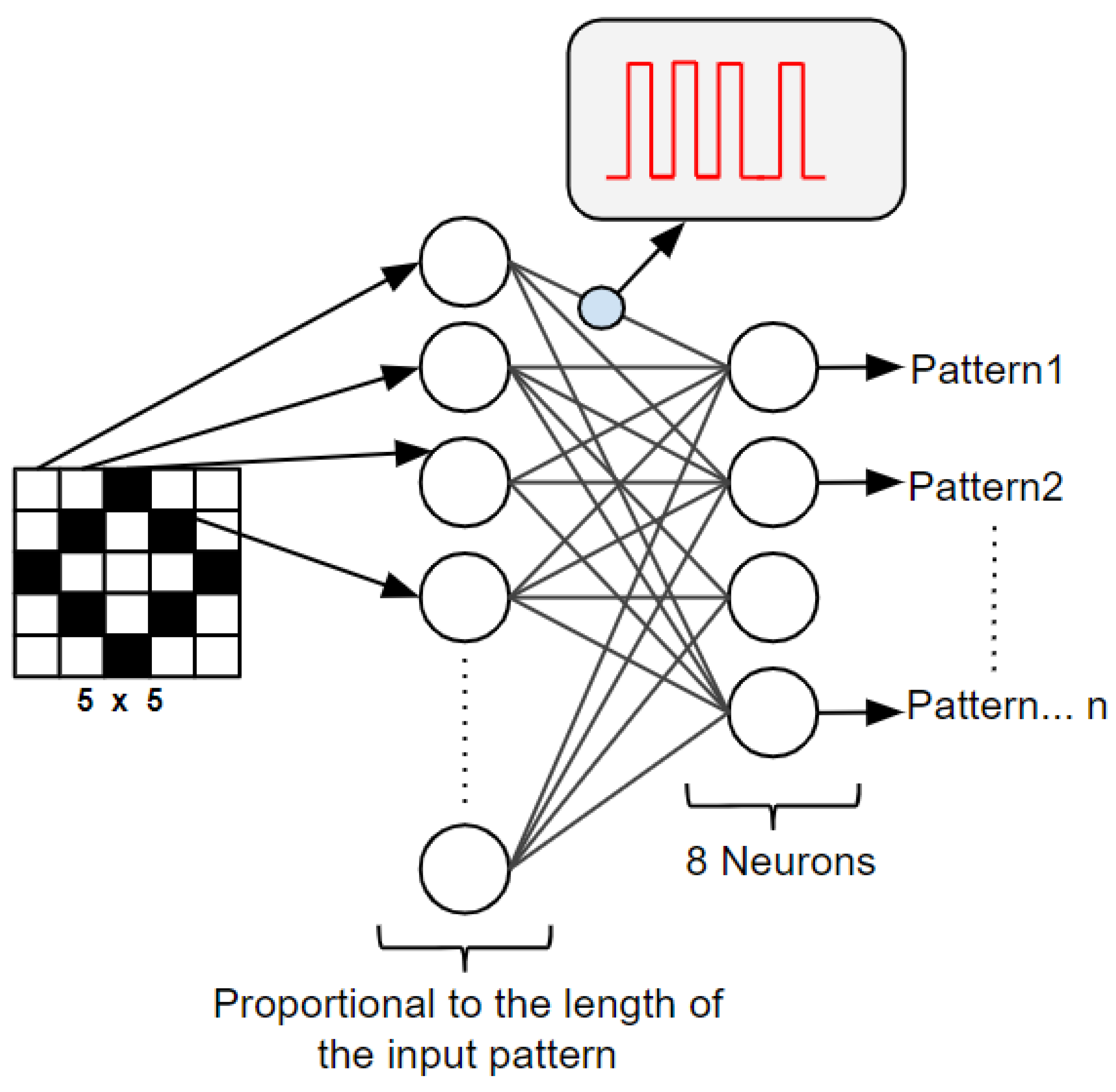
3.4. Implemented WTA Architecture

In this section, a WTA neural network is implemented using both simplified and floating-point neurons. Figure 7 shows the structure of the WTA. This architecture consists of two layers. The first layer is used to encode the black and white pixels of the input patterns to spike trains. The second layer consists of the output neurons, and each output neuron is corresponding to a class. The neurons of the second layer are internally connected through an inhibitory connection. The winner neuron inhibits the increase in the membrane potential of other neurons at the same layer by using these lateral inhibitory connections.
The input layer of the WTA module consists of N neurons and M neurons in the second layer, where N and M are equal to the pattern length and number of classes, respectively. Each pixel of the input pattern is connected to an individual neuron at the input layer. The neurons of the second layer generate spikes in response to the input patterns. The highest rate of spikes shows the winner neuron, and it determines the pattern’s class. The STDP learning algorithm is utilized to train the WTA neural network through an off-chip training method. This procedure is used to obtain the synaptic weights between the input layer and output layer of a WTA neural network.

4. Results and Discussion

In this section, the results of the simulation and implementation are presented. First, the spike rate of the implemented neurons is reported. Next, the functionality of the implemented WTA is evaluated. Finally, the resource consumption of the neurons, synthesized by Xilinx ISE, is provided, and is also compared with related works.

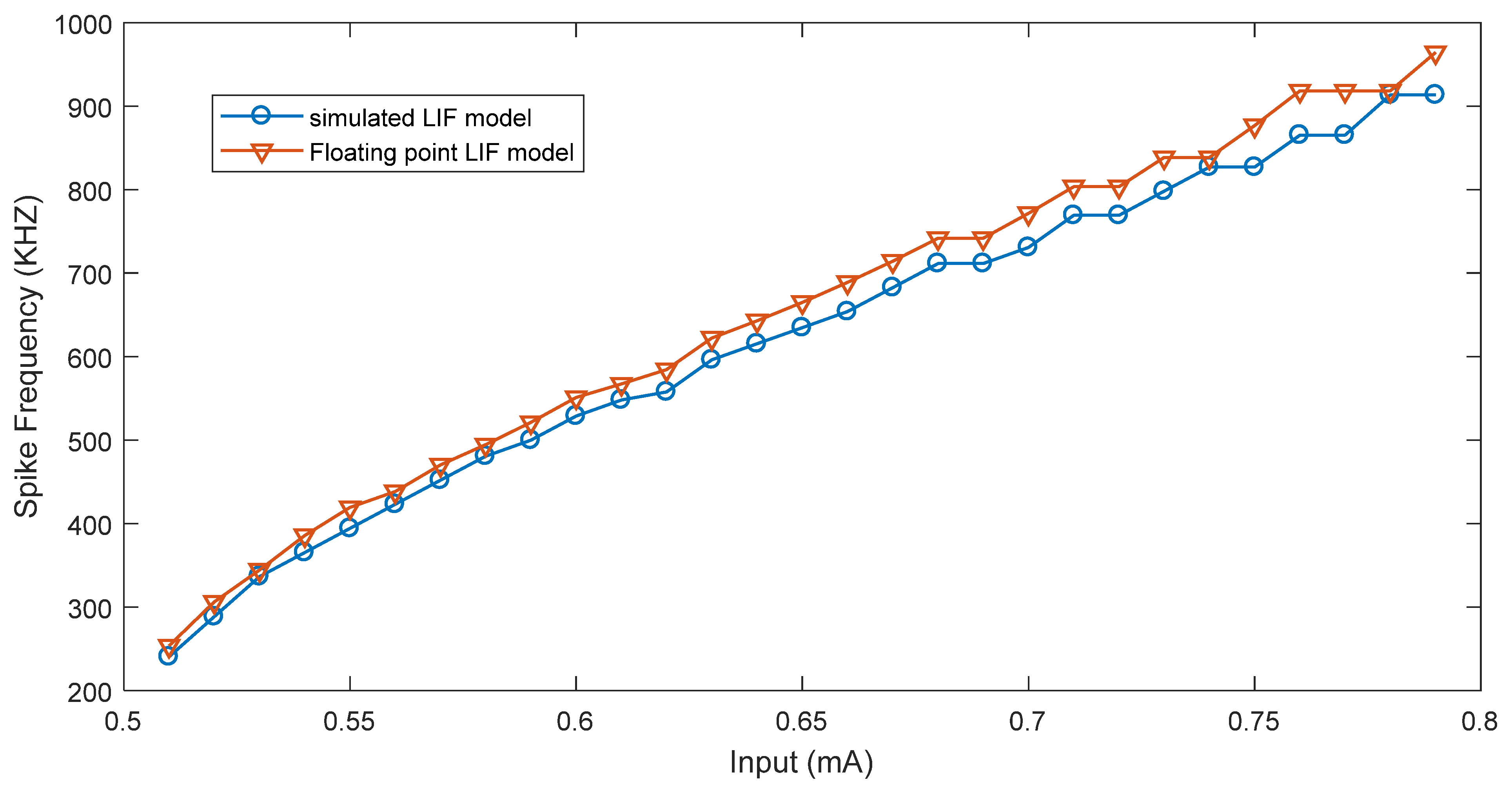
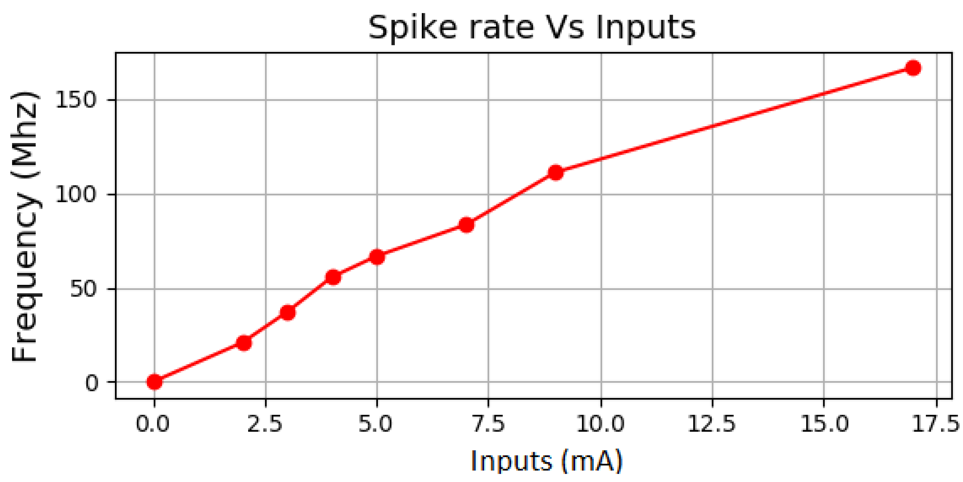
4.1. Spike Rate of the Simplified and Floating-Point Neurons

One of the most important features of an LIF neuron is the proportion of the output spike rate in the response to external stimuli. The rate of output spikes is related to the value of external stimuli. More significant stimuli generate higher spike rates. Thus, the evaluation of this feature for both the floating point and the simplified neuron is considered here. Figure 8 demonstrates the comparison between the spike rates of the implemented floating-point neuron and simulation results using the Tensorflow library in Python. The results show that the implemented floating-point neuron is comparable with the simulation and is able to produce a wide range of spike rates. The input current is altered from 0.5 mA to 0.79 mA and the rate of the output spikes ranges from about 250 kHz to 1 MHz, accordingly. In the LIF model, the refractory period is not considered, which results in a linear relationship between the input current and the output spike rates.
Figure 9 shows the spike rate of the simplified neuron using 𝛼 = 0.937 and 𝛽 = 2. The simplified neuron has a limited rate of spikes due to the nature of fixed-point representation. Although the spike rate of the simplified neuron is not as wide as the floating point, it is applicable to implement SNNs on FPGAs. As it is shown in Figure 9, the input current is altered from 0 to about 17 mA and the neuron is able to produce spike rates from 0 to 166 Mhz. There is also a linear relationship between the input current and output spike rates.
The implementation of the simplified LIF neuron shows that it is able to generate a wide range of spikes at the output of the neuron. Therefore, it preserves the main feature of an LIF model, which is a generation of spike trains proportional to the input current. In the next subsection, the simplified neuron is used in the WTA neural network and the performance of the WTA is evaluated.

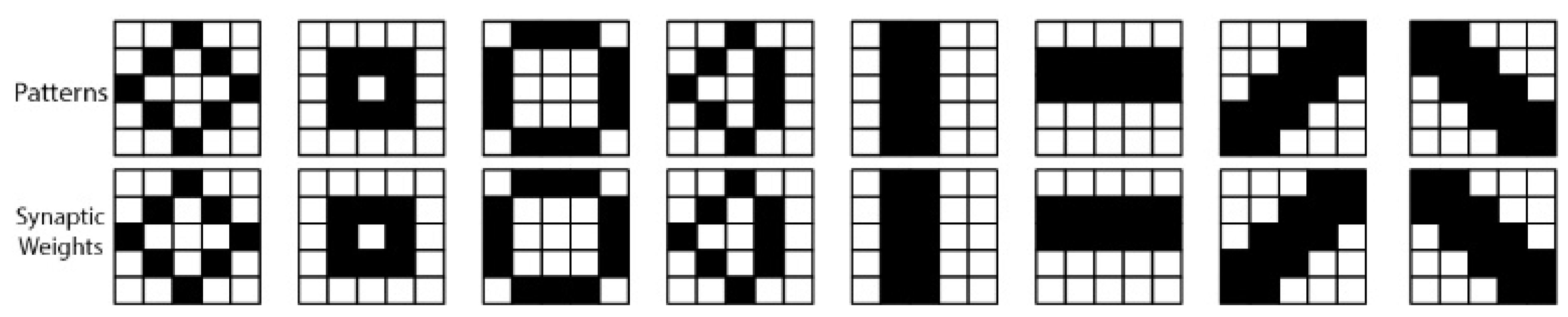
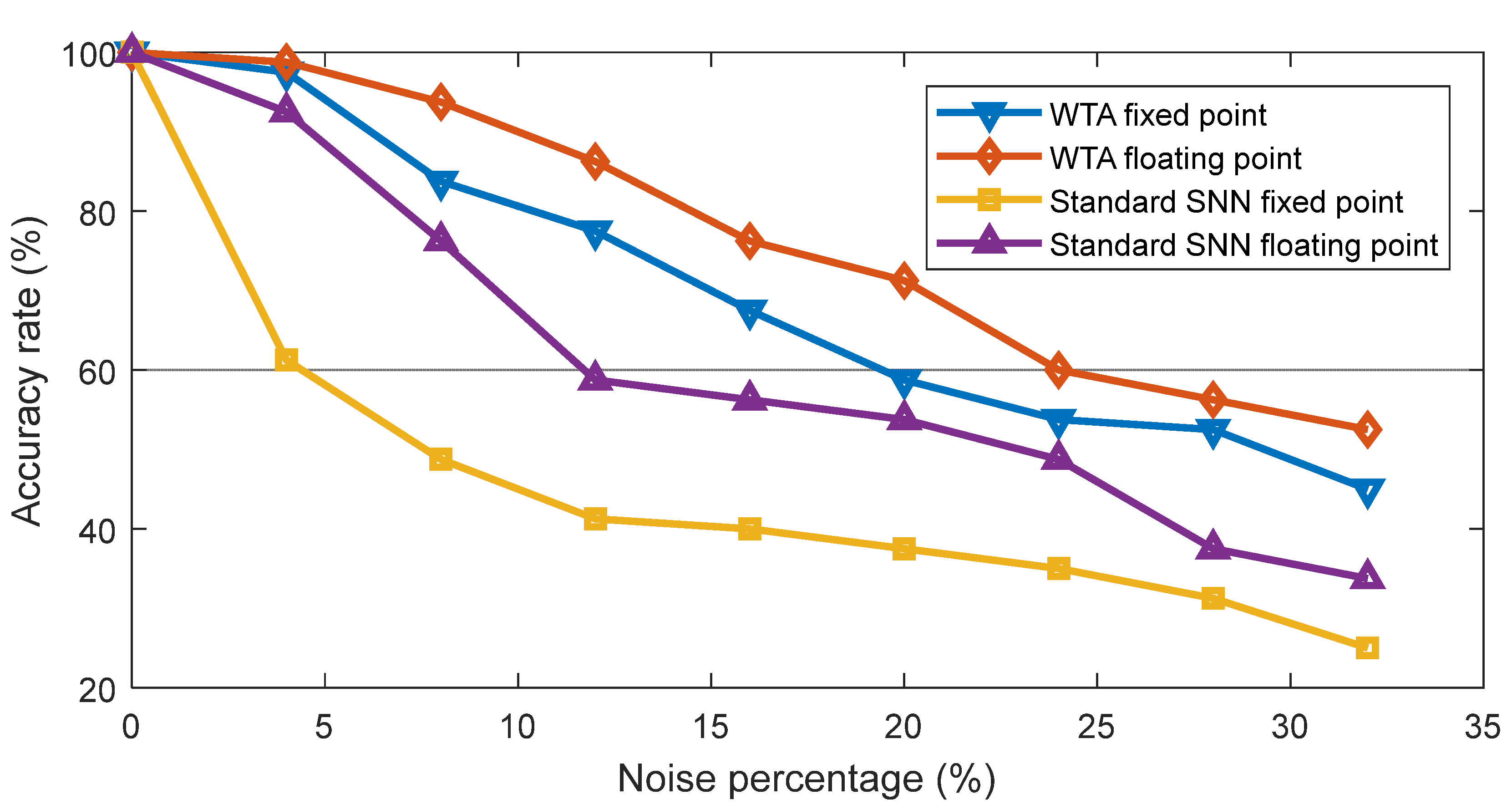
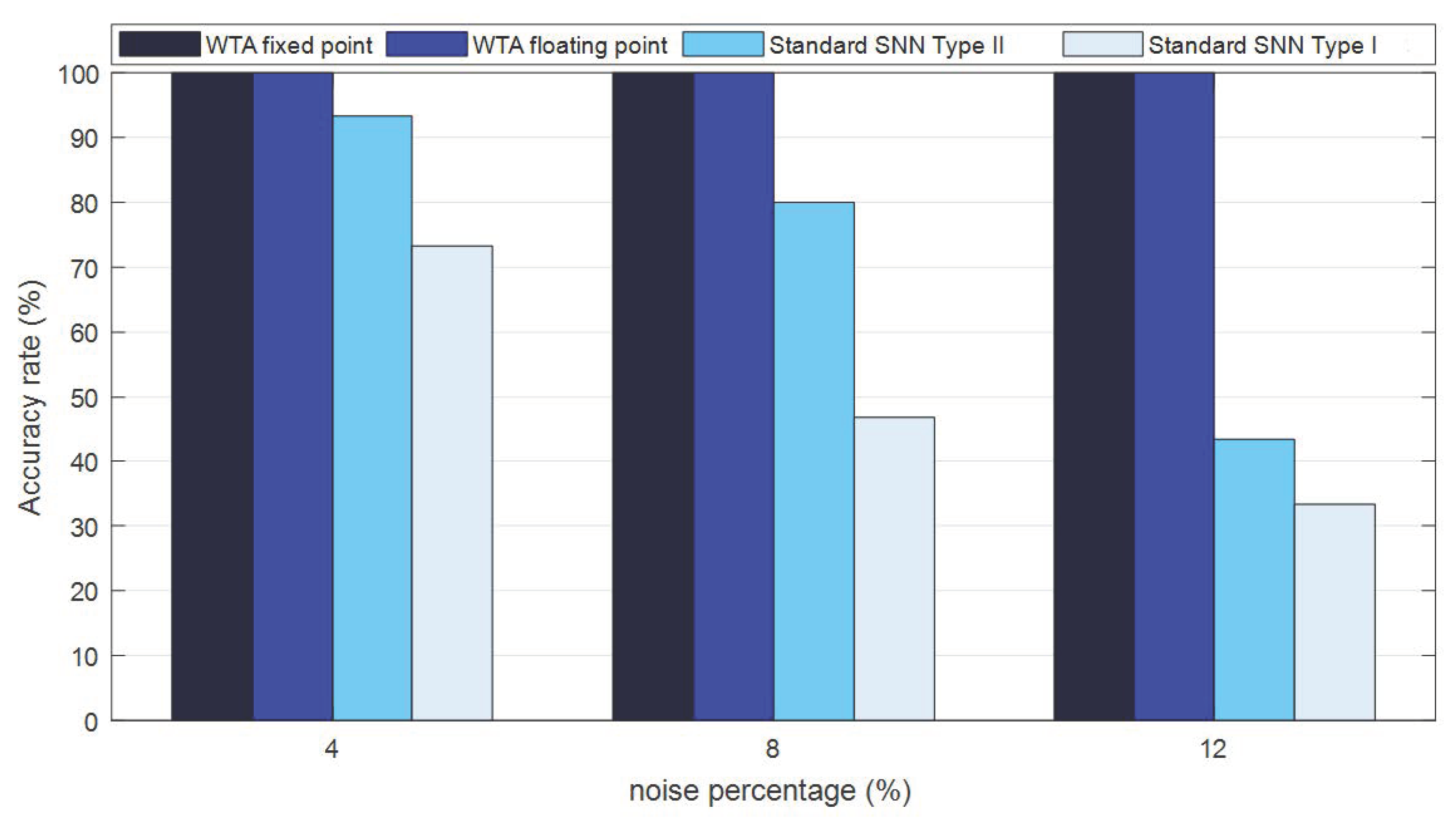
4.2. Recognition Accuracy of the Spiking WTA

In this section, the simplified neuron is utilized to implement spiking neural networks such as spiking WTA. The implemented WTA architecture consists of an input layer and an output layer with eight neurons. In addition, a standard SNN without inhibitory connections (a two-layer SNN, which is used in [16]) is implemented to compare its performance with the spiking WTA. In both architectures, the simplified and floating-point neurons are utilized. The calculated weights are stored as the synaptic weights of the output layer neurons in both architectures.
To evaluate the WTA, a dataset consisting of eight patterns is utilized (the number of patterns is equal to the number of output neurons). Figure 10 shows the patterns (top) and corresponding synaptic weights (bottom). The size of the binary patterns is 5 × 5, which is equal to the number of input neurons. The synaptic weights are calculated using the STDP rule and each weight matrix is stored in an input RAM of an output neuron, shown in Figure 4.
The robustness of the spiking WTA is evaluated using generated patterns that are affected by random noises. In this regard, according to a noise percentage, elements of the patterns are randomly selected and converted from 1 to 0 and vice versa. Indeed, each pixel was selected when a certain amount of noise applied to our patterns. The selected pixels then toggled to a noisy pattern. Figure 11 shows some of the generated noisy patterns.
The evaluation of the recognition accuracy of the WTA shows the applicability of the neuron in the implementation of spiking neural networks.
To evaluate the recognition accuracy, the noisy patterns are applied to the neural networks. Then, the output spikes are obtained, and the winning neuron is determined. If the winning neuron is corresponding to the input pattern, it is considered a correct recognition. The evaluation is repeated ten times for each pattern. Figure 12 shows the recognition accuracy versus the noise percentage for the spiking WTA and the two-layer SNN. Results show that the accuracy of the spiking WTA is better than the standard SNN by almost 27% on average. In addition, using the floating-point neurons produces better accuracy than using the simplified neuron.
In another evaluation, the patterns that are represented in [16] are used, as well. Figure 13 shows a comparison between the proposed WTA and standard SNN [16]. The noise percentages of 4%, 8%, and 12% were applied to the patterns. As shown in Figure 13, the WTA architecture obtains 100% accuracy compared to the architectur. The simulation results show that the accuracy of the WTA architecture is better than the standard SNN [16]. In addition, the floating point enables an SNN to have better accuracy. However, the resource consumption of the simplified neuron is much less than the floating-point neurons and other similar neurons, which is discussed in the next subsection.

4.3. Resource Consumption

One of the main goals of our work is to reduce the amount of resource consumption. For comparison, a Virtex-6 XC6VLX240T is chosen for synthesis and implementation. Table 1 provides the device utilization of the simplified neuron on the device in terms of the utilized registers and LUTs. The results indicate that the resource utilization of the simplified neuron decreases by almost 30 percent compared to related works. In addition, the consumed resources for the simplified neuron are reduced by a factor of 10 compared to the floating-point model. Moreover, a comparison of the maximum frequency of the target device is reported. However, the maximum frequency of the device depends on the device’s technology. To have a fair comparison, the spiking WTA and standard SNN in [16] are implemented on an identical FPGA. Table 2 also provides the resource consumption of the spiking WTA and standard SNN in [16]. According to the results, the operation frequency of the spiking WTA considerably increased. Resource consumption is another factor that is dramatically reduced compared to the standard SNN [16].

5. Conclusions

Considering the importance of the new generation of Metaverse platforms on the edge layer, it is essential to produce more efficient, secure, and reliable equipment to improve the quality of services, especially in the case of performance and energy consumption. One of the most critical components required to provide this potential equipment is their processor. The more efficient a processor is, the better the edge services that can be achieved. Accordingly, a TinyML processor based on a simplified neuron imitating the LIF neuron model has been designed and implemented in this paper. Using the LIF neuron, two different architectures of SNNs in the TinyML processor have been proposed here, including a spiking WTA and a standard SNN. The results showed the desired operation of the proposed processor. The most important contributions of the proposed processor are as follows:
i
Presenting a super-efficient TinyML chip for a wide range of IoTs and smart gadgets to be used in the edge-enabled Metaverse.
ii
Demanding low resource consumption.
iii
High operating frequency and speed.
iv
Increasing the accuracy significantly, making it an ideal option for medical applications in Metaverse applications.
The resource consumption of the proposed simplified LIF neuron is reduced by 30% compared to related works. In addition, evaluations show that the accuracy of the spiking WTA based on the simplified neuron is much better than the standard SNN. The above-mentioned features, along with low resource consumption, which is considered in our proposed neuron, make this model appropriate for implementing SNNs on edge devices with a concentration on edge-based Metaverse platforms.

Author Contributions

Conceptualization of the processor, A.K., conceptualization of its applications and development, M.J.; methodology, A.K. with support of M.J.; software, A.K.; validation, A.K., M.J., and S.B.S.; formal analysis, A.K. and M.J.; investigation, A.K.; resources, M.J.; writing—original draft preparation, A.K. and M.J.; writing—review and editing, S.B.S.; visualization, A.K.; supervision, S.B.S.; project administration, S.B.S. All authors have read and agreed to the published version of the manuscript.

Funding

This research received no external funding.

Conflicts of Interest

The authors declare no conflict of interest.

References

  1. Liu, H.; Wei, Z.; Zhang, H.; Li, B.; Zhao, C. Tiny Machine Learning (Tiny-ML) for Efficient Channel Estimation and Signal Detection. IEEE Trans. Veh. Technol. 2022, 71, 6795–6800. [Google Scholar] [CrossRef]
  2. Ray, P.P. A review on TinyML: State-of-the-art and prospects. J. King Saud Univ.-Comput. Inf. Sci. 2021, 34, 1595–1623. [Google Scholar] [CrossRef]
  3. Dutta, L.; Bharali, S. Tinyml meets iot: A comprehensive survey. Internet Things 2021, 16, 100461. [Google Scholar] [CrossRef]
  4. Asutkar, S.; Chalke, C.; Shivgan, K.; Tallur, S. TinyML-enabled edge implementation of transfer learning framework for domain generalization in machine fault diagnosis. Expert Syst. Appl. 2023, 213, 119016. [Google Scholar] [CrossRef]
  5. Dwivedi, Y.K.; Hughes, L.; Baabdullah, A.M.; Ribeiro-Navarrete, S.; Giannakis, M.; Al-Debei, M.M.; Dennehy, D.; Metri, B.; Buhalis, D.; Cheung, C.M. Metaverse beyond the hype: Multidisciplinary perspectives on emerging challenges, opportunities, and agenda for research, practice and policy. Int. J. Inf. Manag. 2022, 66, 102542. [Google Scholar] [CrossRef]
  6. Shafiei, A.; Jamshidi, M.B.; Khani, F.; Talla, J.; Peroutka, Z.; Gantassi, R.; Baz, M.; Cheikhrouhou, O.; Hamam, H. A Hybrid Technique Based on a Genetic Algorithm for Fuzzy Multiobjective Problems in 5G, Internet of Things, and Mobile Edge Computing. Math. Probl. Eng. 2021, 2021, 9194578. [Google Scholar] [CrossRef]
  7. Shen, S. Metaverse-driven new energy of Chinese traditional culture education: Edge computing method. Evol. Intell. 2022, 1–9. [Google Scholar] [CrossRef]
  8. Zhang, M.; Cao, J.; Sahni, Y.; Chen, Q.; Jiang, S.; Wu, T. Eaas: A service-oriented edge computing framework towards distributed intelligence. In Proceedings of the 2022 IEEE International Conference on Service-Oriented System Engineering (SOSE), Newark, CA, USA, 15–18 August 2022; pp. 165–175. [Google Scholar]
  9. Shamim, M.Z.M. TinyML Model for Classifying Hazardous Volatile Organic Compounds Using Low-Power Embedded Edge Sensors: Perfecting Factory 5.0 Using Edge AI. IEEE Sens. Lett. 2022, 6, 1–4. [Google Scholar] [CrossRef]
  10. Jamshidi, M.B.; Roshani, S.; Talla, J.; Peroutka, Z.; Roshani, S. A novel filter-based power divider for wireless communication in intelligent transportation systems. In Proceedings of the 2020 19th International Conference on Mechatronics-Mechatronika (ME), Prague, Czech Republic, 2–4 December 2020; pp. 1–5. [Google Scholar]
  11. Cassidy, A.S.; Georgiou, J.; Andreou, A.G. Design of silicon brains in the nano-CMOS era: Spiking neurons, learning synapses and neural architecture optimization. Neural Netw. 2013, 45, 4–26. [Google Scholar] [CrossRef]
  12. Karimi, G.; Gholami, M.; Farsa, E.Z. Digital implementation of biologically inspired Wilson model, population behavior, and learning. Int. J. Circuit Theory Appl. 2018, 46, 965–977. [Google Scholar] [CrossRef]
  13. Nouri, M.; Karimi, G.; Ahmadi, A.; Abbott, D. Digital multiplierless implementation of the biological FitzHugh–Nagumo model. Neurocomputing 2015, 165, 468–476. [Google Scholar] [CrossRef]
  14. Hayati, M.; Nouri, M.; Abbott, D.; Haghiri, S. Digital Multiplierless Realization of Two-Coupled Biological Hindmarsh–Rose Neuron Model. IEEE Trans. Circuits Syst. II Express Briefs 2016, 63, 463–467. [Google Scholar] [CrossRef]
  15. Hayati, M.; Nouri, M.; Haghiri, S.; Abbott, D. Digital Multiplierless Realization of Two Coupled Biological Morris-Lecar Neuron Model. IEEE Trans. Circuits Syst. I Regul. Pap. 2015, 62, 1805–1814. [Google Scholar] [CrossRef]
  16. Farsa, E.Z.; Ahmadi, A.; Maleki, M.A.; Gholami, M.; Rad, H.N. A Low-Cost High-Speed Neuromorphic Hardware Based on Spiking Neural Network. IEEE Trans. Circuits Syst. II Express Briefs 2019, 66, 1582–1586. [Google Scholar] [CrossRef]
  17. Zenke, F.; Bohté, S.M.; Clopath, C.; Comşa, I.M.; Göltz, J.; Maass, W.; Masquelier, T.; Naud, R.; Neftci, E.O.; Petrovici, M.A.; et al. Visualizing a joint future of neuroscience and neuromorphic engineering. Neuron 2021, 109, 571–575. [Google Scholar] [CrossRef] [PubMed]
  18. Shafique, M.; Theocharides, T.; Reddy, V.J.; Murmann, B. TinyML: Current Progress, Research Challenges, and Future Roadmap. Proc. Des. Autom. Conf. 2021, 2021, 1303–1306. [Google Scholar] [CrossRef]
  19. Bethi, Y.; Xu, Y.; Cohen, G.; Van Schaik, A.; Afshar, S. An Optimized Deep Spiking Neural Network Architecture without Gradients. IEEE Access 2021, 10, 97912–97929. [Google Scholar] [CrossRef]
  20. Zhang, Y.; Li, S.; Geng, G. Initialization-Based k-Winners-Take-All Neural Network Model Using Modified Gradient Descent. IEEE Trans. Neural Netw. Learn. Syst. 2021, 2021, 1–9. [Google Scholar] [CrossRef] [PubMed]
  21. Rinkus, G.J. A cortical sparse distributed coding model linking mini- and macrocolumn-scale functionality. Front. Neuroanat. 2010, 4, 17. [Google Scholar] [CrossRef] [Green Version]
  22. Abbott, L.F.; Kepler, T.B. Model neurons: From Hodgkin-Huxley to hopfield. In Statistical Mechanics of Neural Networks; Springer: Berlin/Heidelberg, Germany, 1990; pp. 5–18. [Google Scholar] [CrossRef]
  23. Wilson, H.R. Simplified Dynamics of Human and Mammalian Neocortical Neurons. J. Theor. Biol. 1999, 200, 375–388. [Google Scholar] [CrossRef] [PubMed] [Green Version]
  24. Burkitt, A.N. A review of the integrate-and-fire neuron model: I. Homogeneous synaptic input. Biol. Cybern. 2006, 95, 1–19. [Google Scholar] [CrossRef] [PubMed]
  25. Izhikevich, E.M. Simple model of spiking neurons. IEEE Trans. Neural Netw. 2003, 14, 1569–1572. [Google Scholar] [CrossRef] [PubMed] [Green Version]
  26. Guo, T.; Pan, K.; Sun, B.; Wei, L.; Yan, Y.; Zhou, Y.; Wu, Y. Adjustable Leaky-Integrate-and-fire neurons based on memristor-coupled capacitors. Mater. Today Adv. 2021, 12, 100192. [Google Scholar] [CrossRef]
  27. Soro, S. TinyML for Ubiquitous Edge AI, February 2021. [Online]. Available online: https://arxiv.org/abs/2102.01255v1 (accessed on 8 April 2023).
  28. Lim, W.Y.B.; Xiong, Z.; Niyato, D.; Cao, X.; Miao, C.; Sun, S.; Yang, Q. Realizing the Metaverse with Edge Intelligence: A Match Made in Heaven. IEEE Wirel. Commun. 2022, 2022, 1–9. [Google Scholar] [CrossRef]
  29. Khan, L.U.; Han, Z.; Niyato, D.; Hossain, E.; Hong, C.S.; Member, S. Metaverse for Wireless Systems: Vision, Enablers, Architecture, and Future Directions, June 2022. [Online]. Available online: https://arxiv.org/abs/2207.00413v1 (accessed on 8 April 2023).
  30. Xu, M.; Ng, W.C.; Lim, W.Y.B.; Kang, J.; Xiong, Z.; Niyato, D.; Yang, Q.; Shen, X.S.; Miao, C. A Full Dive Into Realizing the Edge-Enabled Metaverse: Visions, Enabling Technologies, and Challenges. IEEE Commun. Surv. Tutorials 2022, 25, 656–700. [Google Scholar] [CrossRef]
  31. Sunyaev, A. Internet Computing: Principles of Distributed Systems and Emerging Internet-Based Technologies. In Internet Computing: Principles of Distributed Systems and Emerging Internet-Based Technologies; Springer: Berlin/Heidelberg, Germany, 2020; pp. 1–413. [Google Scholar] [CrossRef]
  32. Dhelim, S.; Kechadi, T.; Chen, L.; Aung, N.; Ning, H.; Atzori, L. Edge-Enabled Metaverse: The Convergence of Metaverse and Mobile Edge Computing, April 2022. [Online]. Available online: https://arxiv.org/abs/2205.02764v1 (accessed on 8 April 2023).
  33. Fang, Y.; Cohen, M.A.; Kincaid, T.G. Dynamics of a Winner-Take-All Neural Network. Neural Netw. 1996, 9, 1141–1154. [Google Scholar] [CrossRef] [PubMed]
  34. Handrich, S.; Herzog, A.; Wolf, A.; Herrmann, C.S. A biologically plausible winner-takes-all architecture. In Lecture Notes in Computer Science (Including Subseries Lecture Notes in Artificial Intelligence and Lecture Notes in Bioinformatics); Springer: Berlin/Heidelberg, Germany, 2009; Volume 5755, pp. 315–326. [Google Scholar] [CrossRef]
  35. Ng, W.C.; Lim, W.Y.B.; Ng, J.S.; Xiong, Z.; Niyato, D.; Miao, C. Unified Resource Allocation Framework for the Edge Intelligence-Enabled Metaverse. In Proceedings of the IEEE International Conference on Communications, Seoul, Republic of Korea, 16–20 May 2022; pp. 5214–5219. [Google Scholar] [CrossRef]
  36. Chen, Y. Mechanisms of Winner-Take-All and Group Selection in Neuronal Spiking Networks. Front. Comput. Neurosci. 2017, 11, 20. [Google Scholar] [CrossRef] [PubMed] [Green Version]
  37. Shamsi, J.; Mohammadi, K.; Shokouhi, S.B. Columnar-Organized Memory (COM): Brain-inspired associative memory with large capacity and robust retrieval. Biol. Inspired Cogn. Arch. 2017, 20, 39–46. [Google Scholar] [CrossRef]
  38. Wu, X.; Saxena, V.; Zhu, K. Homogeneous Spiking Neuromorphic System for Real-World Pattern Recognition. IEEE J. Emerg. Sel. Top. Circuits Syst. 2015, 5, 254–266. [Google Scholar] [CrossRef] [Green Version]
  39. Diehl, P.U.; Cook, M. Unsupervised learning of digit recognition using spike-timing-dependent plasticity. Front. Comput. Neurosci. 2015, 9, 99. [Google Scholar] [CrossRef] [PubMed] [Green Version]
  40. Shouval, H.Z.; Wang, S.S.-H.; Wittenberg, G.M. Spike timing dependent plasticity: A consequence of more fundamental learning rules. Front. Comput. Neurosci. 2010, 4, 19. [Google Scholar] [CrossRef] [Green Version]
  41. Soleimani, H.; Ahmadi, A.; Bavandpour, M. Biologically Inspired Spiking Neurons: Piecewise Linear Models and Digital Implementation. IEEE Trans. Circuits Syst. I Regul. Pap. 2012, 59, 2991–3004. [Google Scholar] [CrossRef] [Green Version]
  42. Gomar, S.; Ahmadi, A. Digital Multiplierless Implementation of Biological Adaptive-Exponential Neuron Model. IEEE Trans. Circuits Syst. I Regul. Pap. 2013, 61, 1206–1219. [Google Scholar] [CrossRef]
Figure 1. A WTA architecture that can be used in the proposed TinyML chip. The black lines indicate the synaptic connections between the input and output layers. The gray lines show the inhibitory connections of the output neurons.
Information 14 00235 g001
Figure 2. The block diagram of the LIF neuron system. I[z] and Y[z] are the input and output of the system, respectively.
Information 14 00235 g002
Figure 3. The data flow graph of a simplified LIF neuron includes a combination circuit for synaptic multiplication, two multiplexers for increasing and decreasing the membrane potential, two shifters, an adder for multiplication and division, and a comparator for generating output spikes.
Information 14 00235 g003
Figure 4. The combinational circuit for synaptic weight multiplication. The input RAM maintains synaptic weights that are multiplied by the input signal through the parallel AND gates.
Information 14 00235 g004
Figure 5. State diagram of the fixed-point LIF neuron.
Information 14 00235 g005
Figure 6. The architecture of the floating-point LIF neuron.
Information 14 00235 g006
Figure 7. The architecture of the WTA neural network. A pattern is applied to the input layer that generates spikes. An output neuron corresponding to the input pattern is activated accordingly.
Information 14 00235 g007
Figure 8. Spike rates of the implemented floating-point LIF neuron vs. simulation result.
Information 14 00235 g008
Figure 9. Spike rates of the proposed simplified LIF neuron in terms of different inputs (𝛼 = 0.937 and 𝛽 = 2).
Information 14 00235 g009
Figure 10. The applied patterns and synaptic weights for the proposed architecture of the WTA.
Information 14 00235 g010
Figure 11. Randomly generated noisy patterns.
Information 14 00235 g011
Figure 12. Recognition accuracy rate between different types of neural networks.
Information 14 00235 g012
Figure 13. Comparison of the obtained recognition accuracy of the standard SNN in [16] and our spiking WTA.
Information 14 00235 g013
Table 1. Resource comparison of the simplified neuron with the related works.
ModelSlice RegistersSlice LUTsMax Frequency (MHZ)Target Device
NumberUtilizationNumberUtilization
Izhikevich [41]4932%6172%241.9Virtex-II Pro XC2VP30
AdEx [42]3881%12794%190Virtex-II Pro XC2VP30
Morris–Lecar [15]6182%361613%135Virtex-II Pro XC2VP30
FitzHugh–Nagumo [13]52918%108538%-Virtex-II Pro XC2VP30
Hindmarsh–Rose [14]4311%6592%81.2Virtex-II Pro XC2VP30
Wilson [12]3650%6110%98Virtex-6 ML605
Leaky Integrate and Fire [16]460%560%412.371Virtex-6 ML605
This work (fixed-point model)171%361%576.319Virtex-6 XC6VLX240T
This work (floating-point model)2661%4171%314.095Virtex-6 XC6VLX240T
Table 2. Comparison between different types of SNNs in terms of resource utilization and operation frequency.
Logic UtilizationWTA Fixed-PointWTA Floating-PointStandard SNN [16]
Number of Slice Registers20420161023
Number of Slice LUTs350176711,339
Number of BUFG/BUFGCTRLs131
Max Frequency (MHz)514.095 MHz443.941 MHz189.071 MHz
Disclaimer/Publisher’s Note: The statements, opinions and data contained in all publications are solely those of the individual author(s) and contributor(s) and not of MDPI and/or the editor(s). MDPI and/or the editor(s) disclaim responsibility for any injury to people or property resulting from any ideas, methods, instructions or products referred to in the content.

