1. Introduction
The DC–DC converter is a power conversion device that converts the received DC voltage to a DC voltage required by the system for transferring energy to the load [
1]. It is used in several electronic devices for stabilizing the operation of systems; this can range from high-power applications such as solar photovoltaics, electric vehicles, and energy storage systems to low-power applications such as laptops, mobile phones, and portable batteries [
2]. DC–DC converters are becoming miniaturized, and these parts are becoming denser because of the weight reduction and miniaturization of various application products [
3]. DC–DC converters require high-power conversion efficiency for the reduction of energy consumption and long life [
4]. Such high power-conversion efficiency is an important factor for a high-performance high-reliability DC–DC converter [
5,
6].
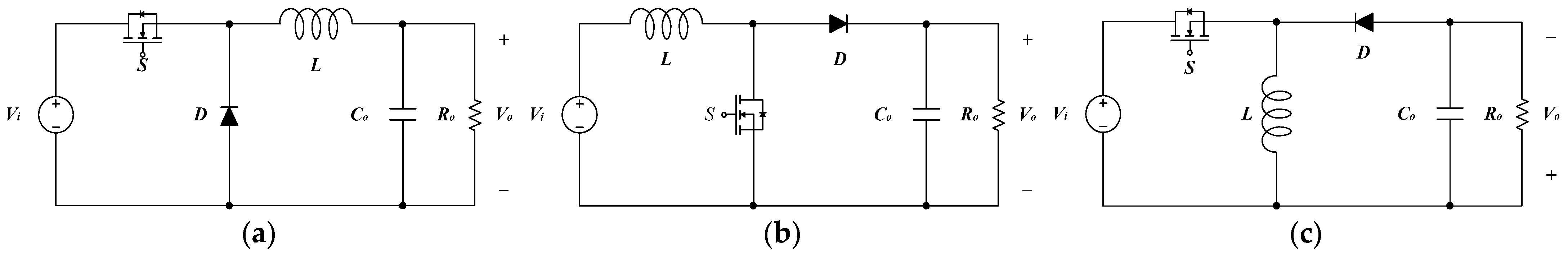
There are three topologies for non-isolated-type DC–DC converters: buck for step-down, boost for step-up, and buck-boost for both step-down and step-up.
Figure 1 shows the circuit diagrams of each topology that consists of a switch, a diode, an inductor, and a capacitor. Step-down and step-up are determined by the duty ratio (d) and wiring of the semiconductors.
Table 1 summarizes the current path and gain (G) of each topology based on switch operation; these topologies of the single switch type should be selected based on the input and output voltage specifications of the system; it is difficult to switch between topologies owing to the fixed element connection. Buck-boost topology with both step-down and step-up cannot be used in applications that require an output voltage of the same polarity as the input voltage because the polarity of the output voltage is opposite to that of the input voltage. Moreover, the power conversion efficiency decreases compared to that of other topologies because the voltage stress of the switch and diode equals the sum of the input voltage
and output voltage
. Therefore, the TSBB converter that can switch to a different topology based on system requirements is used frequently [
7,
8,
9,
10].
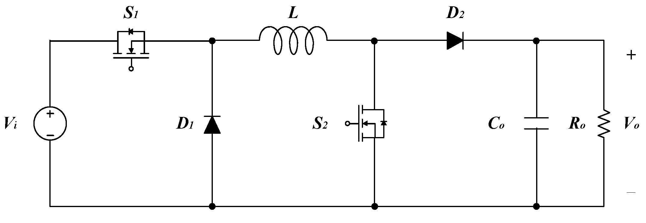
Figure 2 shows a circuit diagram of a conventional TSBB converter that comprises two switches, two diodes, an inductor, and a capacitor. This TSBB converter operates in the buck, boost, or buck-boost topology based on the operation of the switch [
5,
6,
7].
Table 2 summarizes the switching operations of the conventional TSBB converter; it operates in the buck topology by the on/off switching of S
1 while S
2 is always off, and in boost topology by the on/off switching of S
2 while S
1 is always on. Further, the TSBB converter operates in the buck-boost topology by the on/off switching of both S
1 and S
2. It is easy to change the topology despite the increase in parts; the output voltage has the same polarity as the input in the buck-boost topology. Moreover, it is easy to select semiconductors because the voltage stress of the parts does not exceed the input voltage
and output voltage
[
9,
10,
11,
12,
13].
Table 3 presents the switching and conduction semiconductors in each topology of a single switch converter and a TSBB converter. The TSBB converter uses more parts than the single switch converter in each topology owing to the composition and wiring of the semiconductors; this increases the power loss and lowers the power efficiency. The loss of the TSBB converter increases because of the amount of the conduction loss of one diode than the single switch type in the buck topology and the amount of the conduction loss of one switch in the boost topology. Moreover, the power efficiency in the buck-boost topology decreases owing to the switching and conduction losses of one switch and one diode [
5,
6,
10].
New circuits are suggested in [
5,
6] to prevent such a decrease in power efficiency. They demonstrated that power efficiency can be increased compared to those of the conventional TSBB converter by reducing the number of switching and conduction semiconductors in the current path. However, there is a trade-off between the number of semiconductors in the current path and the voltage stress. Therefore, in the new circuits of [
5,
6], the voltage stress of the semiconductors in the boost and buck-boost topologies increases, and it will lower power efficiency above a specific power range. The experimental results confirm the efficiency based on changes in the output current; however, it is difficult to find the optimal power range according to the changes in the input voltage and duty that influence the voltage stress of the semiconductors. To solve this problem, this study proposed a new type of TSBB converter for improving power efficiency and analyzing the optimal power range that can improve power efficiency. The proposed TSBB converter can increase power efficiency in buck and buck-boost topologies by reducing conduction loss caused by the diode in the switch-off section while using the same number of semiconductors as that of the conventional TSBB converter. Moreover, the optimal power range of each topology is analyzed by evaluating the effect of an increase in the voltage stress of semiconductors.
The contributions of this study are as follows:
We investigated related research about the TSBB converter and proposed a modified design of the TSBB converter to improve power efficiency using fewer conduction components in the current path.
We presented the optimal power range according to the buck, boost, and buck-boost topologies in CV and CC modes, and, in particular, divided into step-up/step-down sections in the buck-boost topology.
We analyzed the power dissipation of the three topologies and explained why the CC mode of the buck-boost step-up is less efficient than conventional converters over a certain power range through analytic and experimental diode stress analysis.
The remainder of this paper is organized as follows.
Section 2 describes the operation principle of the proposed TSBB converter. In
Section 3, the power loss is compared between the proposed TSBB converter and the conventional TSBB converter in each topology by analyzing the switching and conduction losses. The experiment results are described in
Section 4, and, finally, the conclusions are presented in
Section 5.
2. Operation Principle
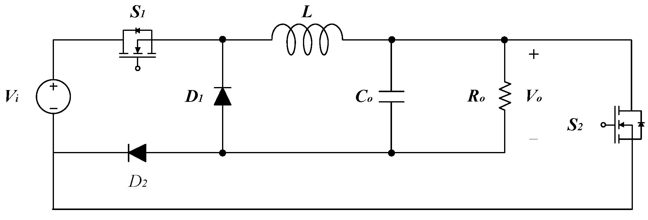
Figure 3 shows the circuit diagram of the proposed TSBB converter. Like the conventional TSBB converter, the proposed TSBB converter is composed of two switches, two diodes, an inductor, and a capacitor; further, it operates in three topologies based on the switching of S
1 and S
2, and it operates in the buck topology by the on/off switching of S
1, in the boost topology by the switching of S
2, and in the buck-boost topology by the simultaneous on/off switching of S
1 and S
2.
Table 4 summarizes the switching operations of the proposed TSBB converter.
Table 4 indicates that the switching operations of S
1, S
2, and D
1 are the same as those of the conventional TSBB converter. However, D
2 performs on/off switching in the buck topology and is always off in the buck-boost topology.
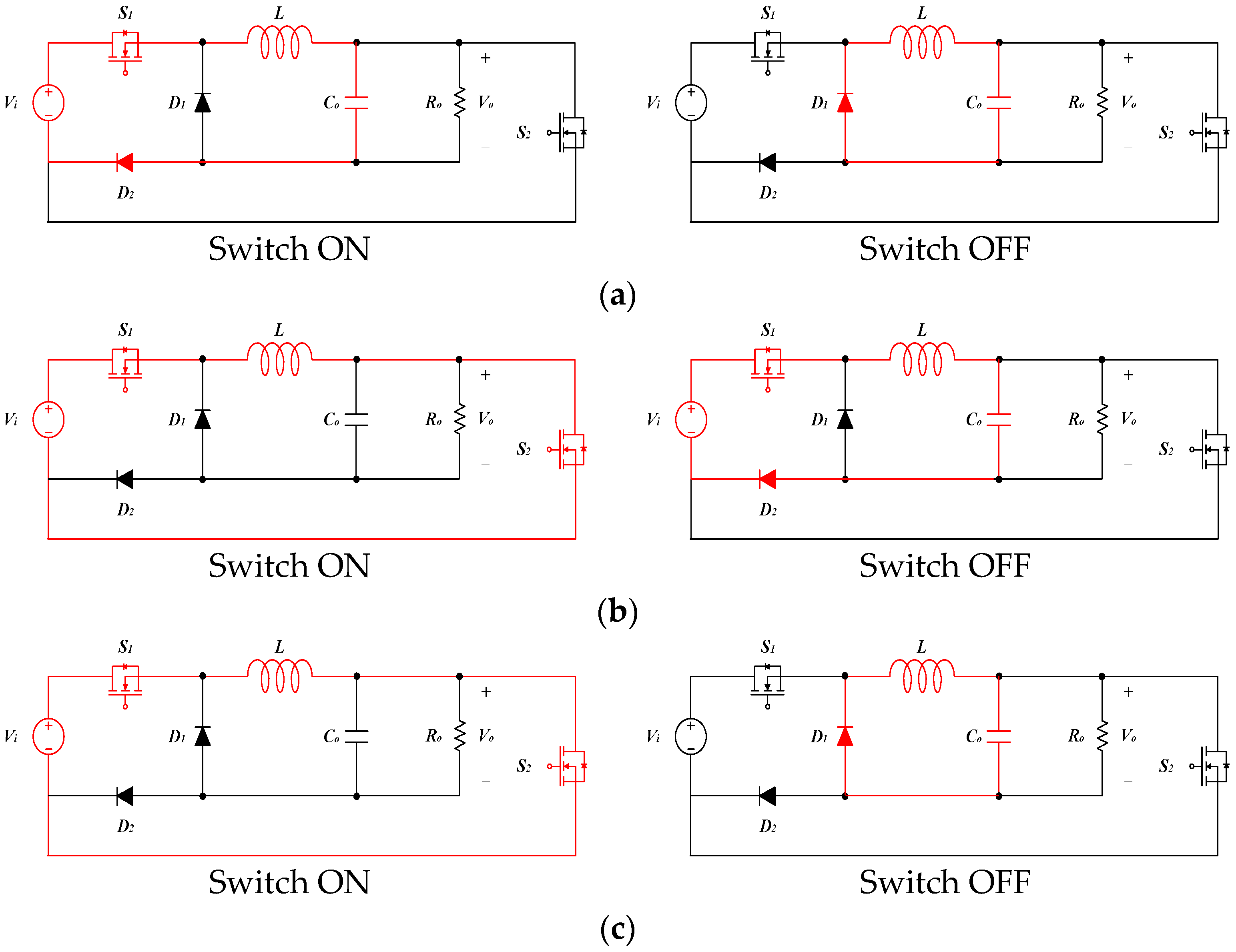
Figure 4 presents the operation principle of the proposed TSBB converter in each topology. The switch-on/off sections are divided by the operation of the switch that transfers the energy to the inductor. The semiconductors located in the current path in each section are conduction semiconductors; the semiconductor that only operates in one of the switch-on/off sections is the switching semiconductor.
Table 5 compares the switching and conduction semiconductors between the conventional and proposed TSBB converters. In comparison with the conventional TSBB converter, the proposed TSBB converter undergoes an increase in the switching loss of D
2 in the switch-on section and a decrease in the conduction loss of D
2 in the switch-off section. In the buck-boost topology, the switching and conduction losses of D
2 in the switch-off section decrease.
Table 6 compares the stress between the conventional and proposed TSBB converters; they have the almost same voltage stress in buck and boost topologies, but in the buck-boost topology, the stress of D
1 increases to
.
3. Analysis of Semiconductor Power Loss
The power loss of a TSBB converter includes the losses of the switch, diode, inductor, and capacitor when various parasitic components in the circuit are ignored. The power loss of the two converters is determined by the power loss of the semiconductors assuming that the losses of the inductor and capacitor are the same between the conventional and proposed TSBB converters. Therefore, the increase or decrease in power efficiency is determined by the operation of the switch and diode.
3.1. Switch and Diode Current
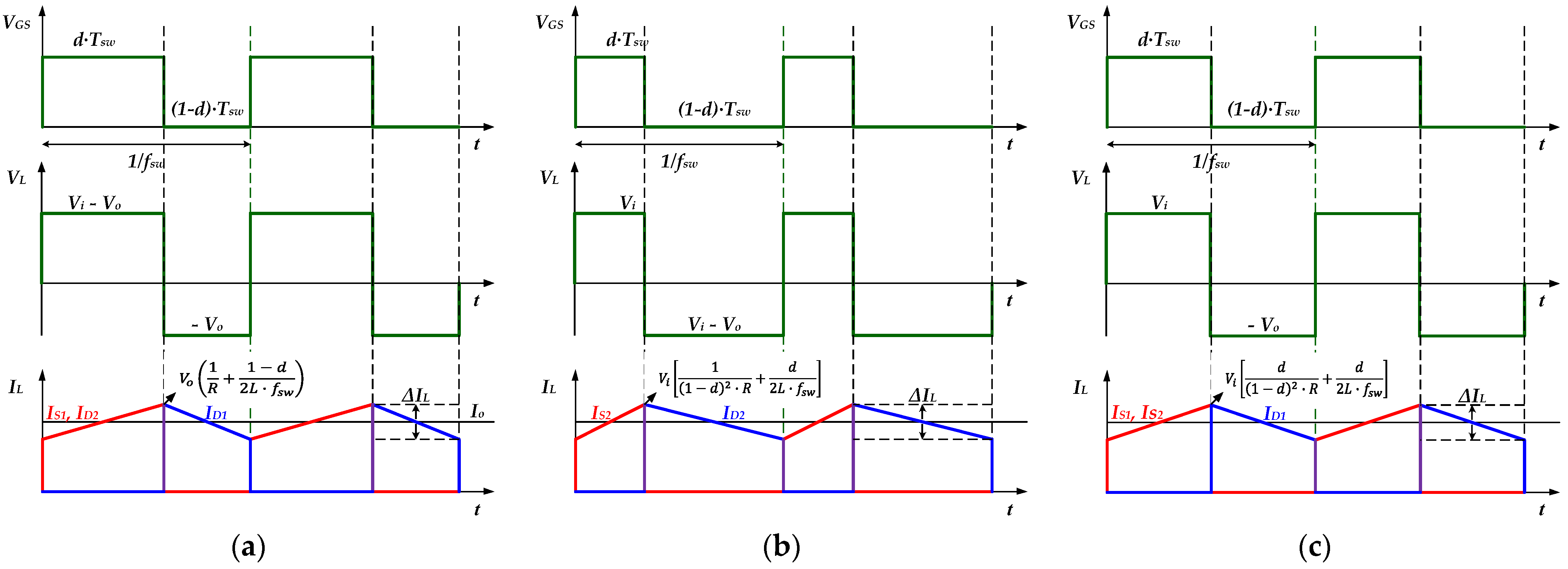
Figure 5 presents the switch and diode current of the proposed TSBB converter in each topology. In the buck topology, the inductor current flows through S
1 and D
2 during the switch-on section and through D
1 during the switch-off section. The inductor current
is the output current
and
by the volt-sec balance law at switching frequency
, the inductor current
,
flowing through switch S
1 and diode D
1/D
2 can be expressed as:
The inductor current flows through S
1 and D
2 during the switch-on section and through D
1 during the switch-off section in the boost topology. Since the inductor current
is
and
, the inductor current
,
flowing through switch S
1/S
2 and diode D
2 can be expressed as:
In buck-boost topology, the inductor current flows through S
1 and D
2 during the switch-on section and through D
1 during the switch-off section. Since the inductor current
and
same as boost topology, the inductor current
,
flowing through switch S
1/S
2 and diode D
2 can be expressed as:
The power loss of a TSBB converter includes the losses of the switch, diode, inductor, and capacitor when various parasitic components in the circuit are ignored. The power loss of the two converters is determined by the power loss of the semiconductors assuming that the losses of the inductor and capacitor are the same between the conventional and proposed TSBB converters. Therefore, the increase or decrease in the power efficiency is determined by the operation of the switch and diode.
The losses of semiconductors are divided into switching and conduction losses. A switching loss occurs during the transient time of the switching operation. Although the switching loss is 0 in the ideal condition, it is caused by the time delay attributed to the parasitic resistance and parasitic capacitance at the time of turn-on or turn-off [
14,
15]. The conduction loss is caused by the current that flows by the turn-on of the semiconductor and on the resistance of the semiconductor [
16,
17,
18].
3.2. Switching Loss
The switching loss of MOSFET,
is divided into switch turn-on loss,
switch turn-off loss
, and output capacitance loss
as [
5,
15,
17]:
The switch turn-on and turn-off losses are difficult to calculate because of the nonlinear characteristics of the drain-source voltage
and drain current
. Therefore, they can be determined by applying linear approximation in the rising and falling sections of
and
. The output capacitance loss of MOSFET can be determined by calculating the stored energy of the capacitor because the energy is charged in the output capacitance when the MOSFET turns off, and is discharged when the MOSFET turns on. The MOSFET switching loss can be represented by using the turn-on time
, turn-off time
, switching frequency
, and output capacitance
of the MOSFET as [
5,
17,
18]:
The output capacitance of the MOSFET is several tens to hundreds of picofarads. Therefore, it is negligible compared to the switch turn-on and turn-off losses and can be represented as [
5,
6,
17,
18]:
The switching loss
of the diode can be divided into the switch turn-on loss
and the switch turn-off loss
it is represented as:
The switching loss of the diode can be approximated as the switch turn-off loss because the loss of the diode caused by the reverse recovery in the turn-off section is considerably larger than the turn-on loss [
19,
20].
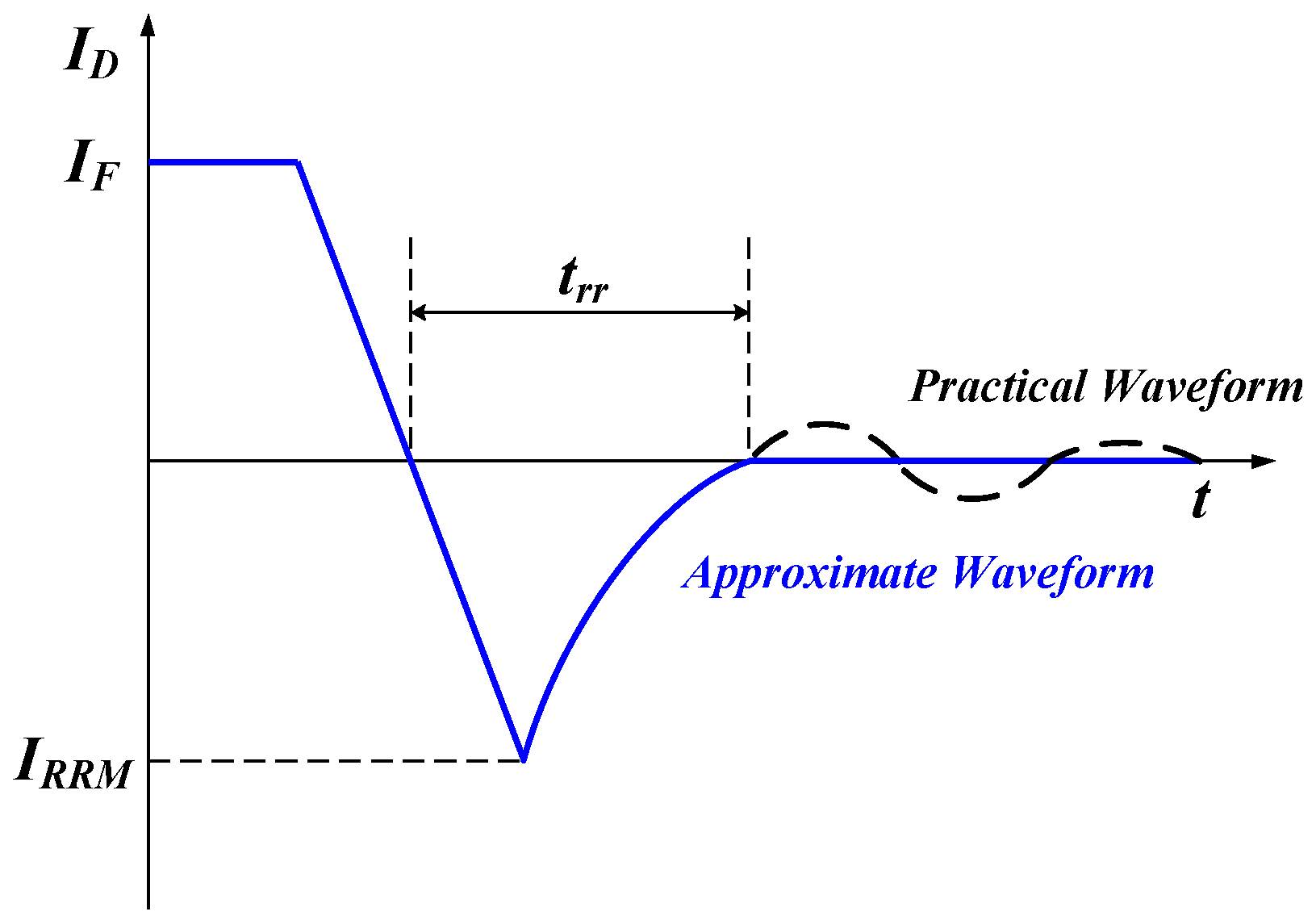
Figure 6 shows the reverse recovery characteristic of the diode [
6]. In an ideal diode, the current flows when the voltage is applied in the forward direction, and no current flows when the voltage is applied in the reverse direction. However, in an actual operation, the reverse current flows for a certain time before it reaches zero when the diode is turned off after a forward current flow. Here, the time during which the reverse current flows is referred to as the reverse recovery time (
); the maximum value of the reverse current that flows in the diode is referred to as the repetitive peak reverse current (
). The turn-off loss
of the diode when the reverse voltage applied to the diode is
and the switching frequency is
can be expressed as [
21,
22]:
3.3. Conduction Loss
The instantaneous value of the conduction loss of the MOSFET,
can be expressed by
,
and the drain-source resistance
in the complete switch turn-off section as [
6,
15,
16,
19]:
The average value can be determined by integrating Equation (6) over the switching period
as:
The instantaneous value of the conduction loss of the diode
can be expressed by the forward voltage drop
, forward current
, and diode resistance
as [
5,
6]:
The average value can be determined by integrating Equation (8) over the switching period
as [
5,
12,
15]:
4. Analysis of Power Loss in Topologies
Table 5 summarizes the switching and conduction semiconductors of the conventional and proposed TSBB converters in each topology.
Table 6 presents the voltage and current stresses of the conventional and proposed TSBB converters in each topology. In each topology, the switching loss that has reflected the voltage stress and conduction loss based on the switch on/off time can be determined and compared.
4.1. Buck Topology
In
Table 5, the switching semiconductors of the conventional TSBB converter are S
1/D
1, and the conducting semiconductors are S
1/D
1/D
2. Thus, the switching loss
and conduction loss
can be expressed, respectively, as:
The switching semiconductors of the proposed TSBB converter are S
1/D
1/D
2, and those of the conducting semiconductor are S
1/D
1/D
2. Therefore, the switching loss
and conduction loss
can be expressed as:
The switching loss varies by the voltage stress; however, the internal voltage of semiconductors is
for both the conventional and proposed TSBB converters. Consequently, the switching losses of the semiconductors are the same. Therefore, the difference in power loss between the two converters can be expressed as:
This difference can be determined by the conduction and switching losses in the switch-off section of D2. Since the switch-off section is , the lower the duty ratio, the higher the efficiency of the proposed TSBB converter.
4.2. Boost Topology
In the boost topology, the switching semiconductors are S
2/D
2, and the conducting semiconductors are S
1/S
2/D
2. Thus, the switching loss
and the conduction loss
can be expressed as:
There is no difference in the efficiency between the conventional and proposed TSBB converters because there is no change in the operation of semiconductors.
4.3. Buck-Boost Topology
In
Table 5, both the switching and conducting semiconductors of the conventional TSBB converter are S
1/S
2/D
1/D
2. Therefore, the switching loss
and conduction loss
can be expressed as:
Both the switching and conducting semiconductors of the proposed TSBB converter are S
1/S
2/D
1. Therefore, the switching loss
and conduction loss
can be, respectively, expressed as:
The voltage stress of each semiconductor is indicated in parentheses since the switching loss varies by the voltage stress. The loss difference between the conventional and proposed TSBB converters is determined by the switching loss of D
1/D
2 and the conduction loss of D
2 in the switch-off section, and it can be expressed as:
There are no switching and conduction losses by D2 because the proposed TSBB converter D2 does not operate. However, the voltage stress of D1 increases to , the voltage stress and reverse current of the diode in a linear section are . Therefore, the loss is determined by the conduction loss of the switch-off section of D2. The power efficiency of the proposed TSBB converter is higher than that of the conventional TSBB converter. In contrast, the switching loss by D1, , increases in the section where the reverse current of the diode increases sharply owing to the voltage stress. Therefore, the power efficiency of the proposed TSBB converter is lower than that of the conventional TSBB converter.
5. Experimental Results
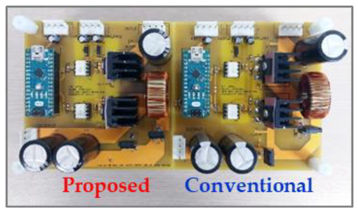
Figure 7 shows a prototype of a 100 W TSBB converter fabricated to verify the improved power efficiency. The Arduino controller generates a 5 V pulse width modulation (PWM) to control the MOSFET driver IC input; upon receiving this signal, the MOSFET driver IC converts it to an 18 V drive signal and transfers it to the gate of the MOSFET. The specifications of the components are 20% or more larger than the calculated maximum stress considering the various input/output conditions of the experiment.
Table 7 summarizes the detailed specifications of the components;
Table 8 presents the maximum values of the voltage stress measured in the CV/CC modes.
The experiments are conducted in the CV/CC modes of the three topologies. The experiment for the buck-boost topology is conducted separately for the step-down and step-up sections. In the CV mode, the power efficiency is measured for the output power range of 10–80 W at the switching frequency
= 100 kHz of the output current. The power efficiency was measured at three duty ratios to analyze the power efficiency based on the change in the duty ratio. If the input/output voltage variation ratio
is defined as the ratio of the difference between the input and output voltages to the input voltage, it can be expressed using the input voltage
and the output voltage
as:
In each topology, the power efficiency was measured at the duty ratios where
was 25%, 33%, and 50%.
Table 9 shows the duty ratio based on
in each topology.
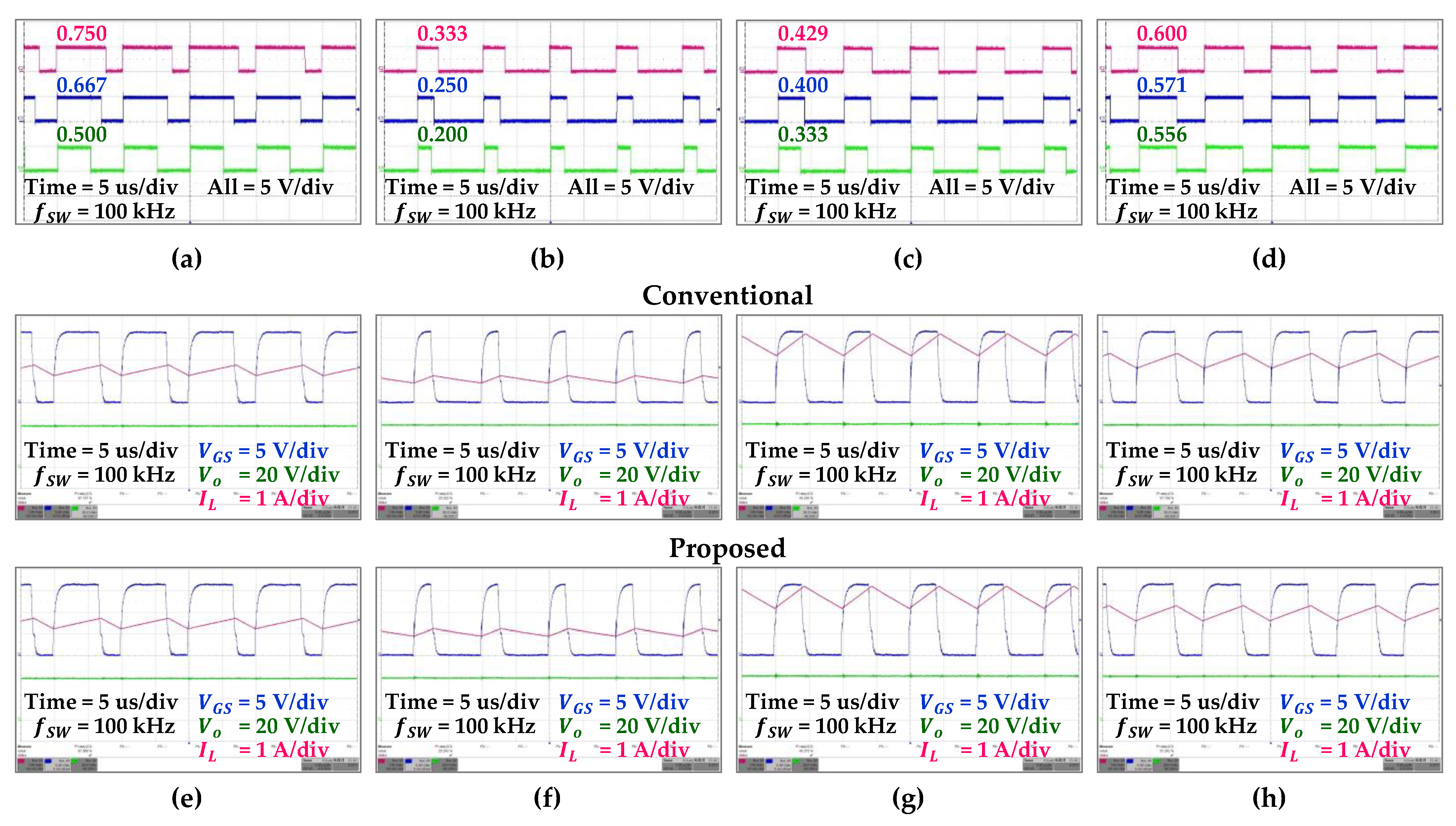
Figure 8a–d shows PWM waveforms of the conventional and the proposed TSBB converter in each topology implemented using Arduino Nano.
Figure 8e–h presents waveforms of the inductor current, the gate-source voltage, and the output voltage of the conventional and proposed TSBB converters measured in CC mode at
= 33% (
40 V).
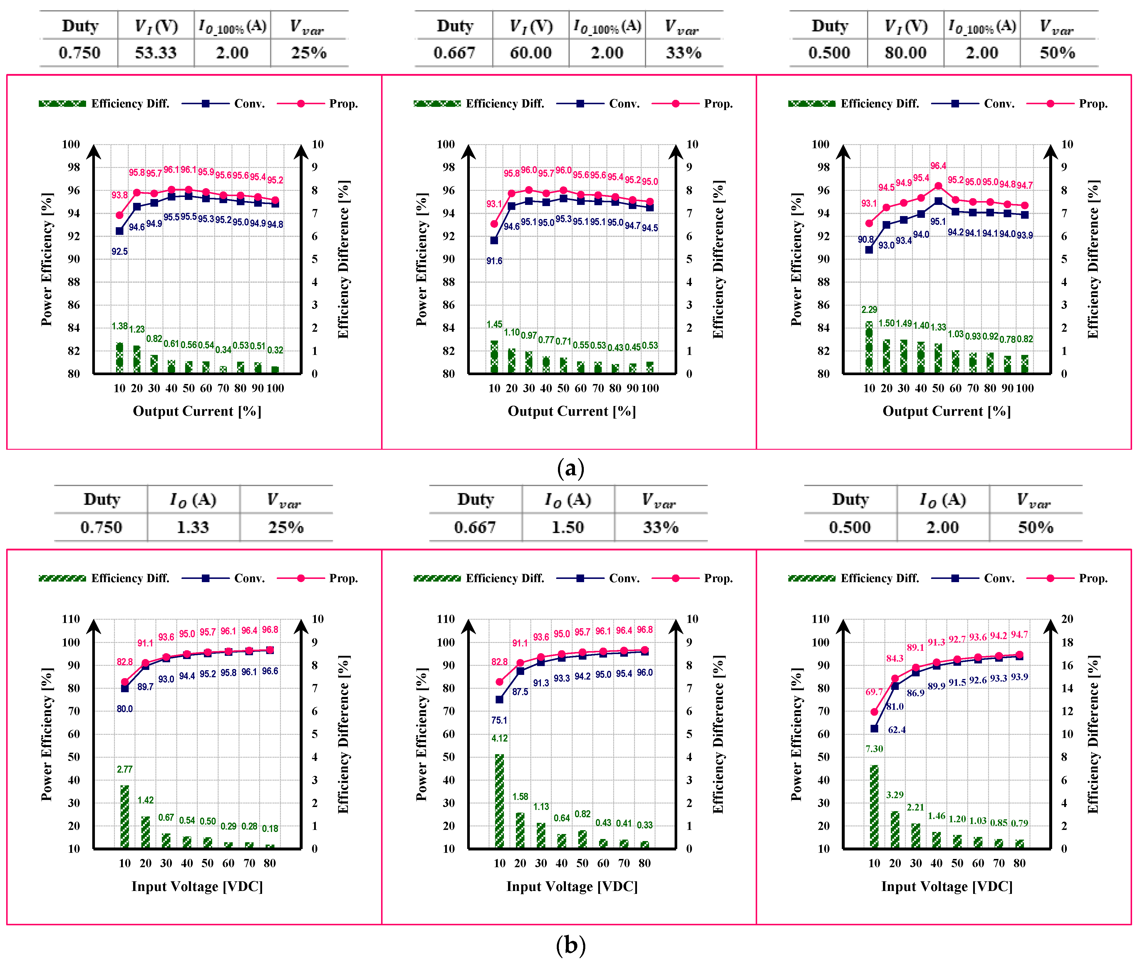
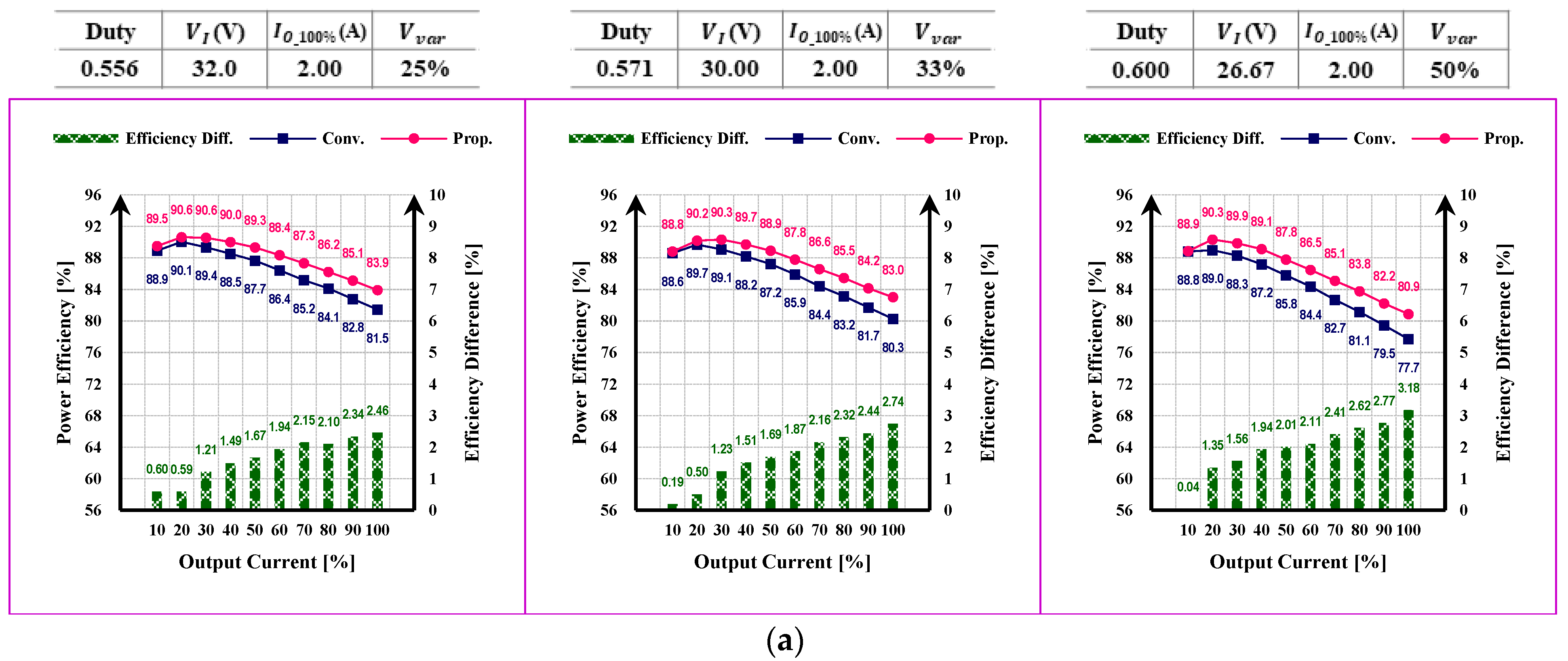
5.1. Buck Topology
Figure 9 shows the power efficiency of the buck topology in the CV and CC modes. If the power efficiency difference
is positive (+), it means efficiency improvement; if it is negative (-), it indicates an efficiency decline. The power efficiency improves in every condition from 10–80 W because of the removal of D
2 in the switch-off section in the CV and CC modes.
increases as the switch-off section becomes longer, i.e., when there is an increase in the duty ratio. In the same duty ratio condition,
decreases with an increase in the input voltage and output current. The improvement effect is large in the low-power region. The proposed converter can achieve a greater efficiency improvement effect in a region where the voltage conversion is large, and the output current is low.
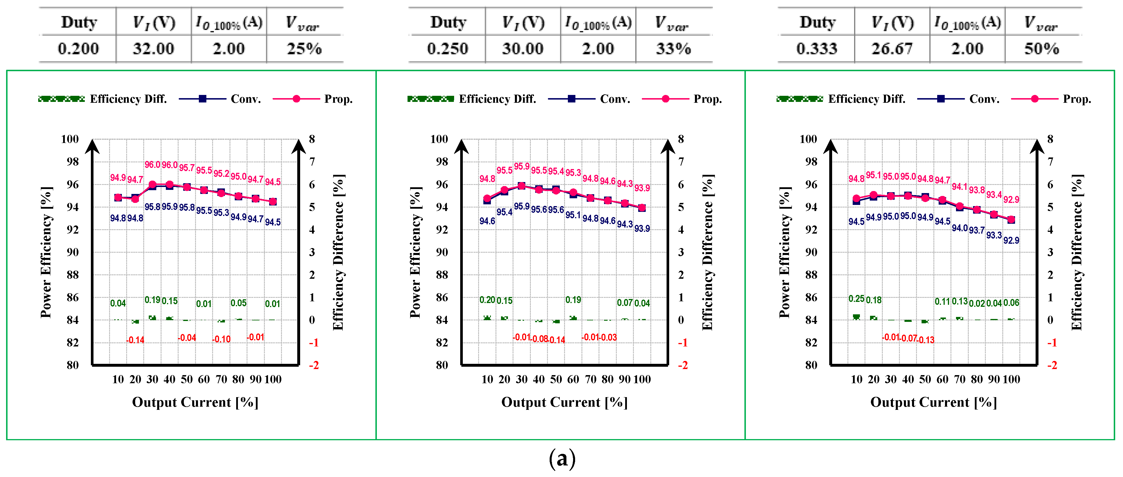
5.2. Boost Topology
Figure 10 shows the power efficiency of the boost topology. The proposed converter shows the same power efficiency in the measured error range because it has the same number of semiconductors and the same stress as the conventional converter.
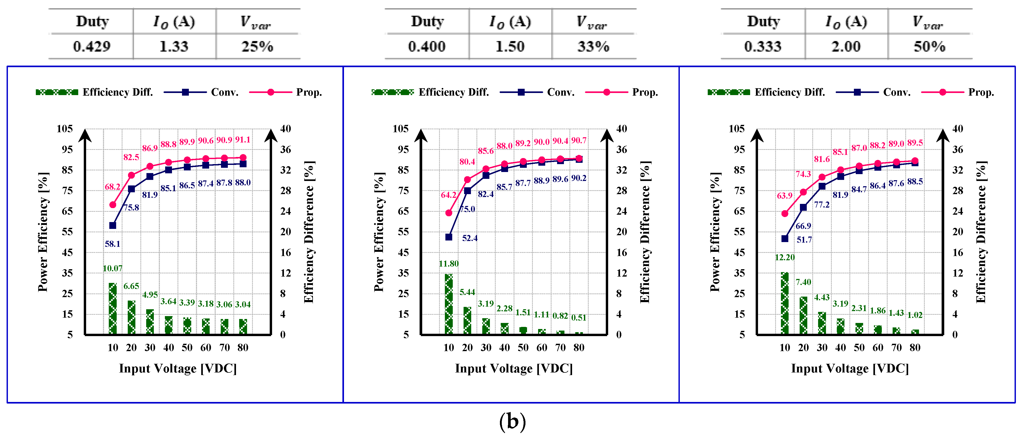
5.3. Buck-Boost Topology
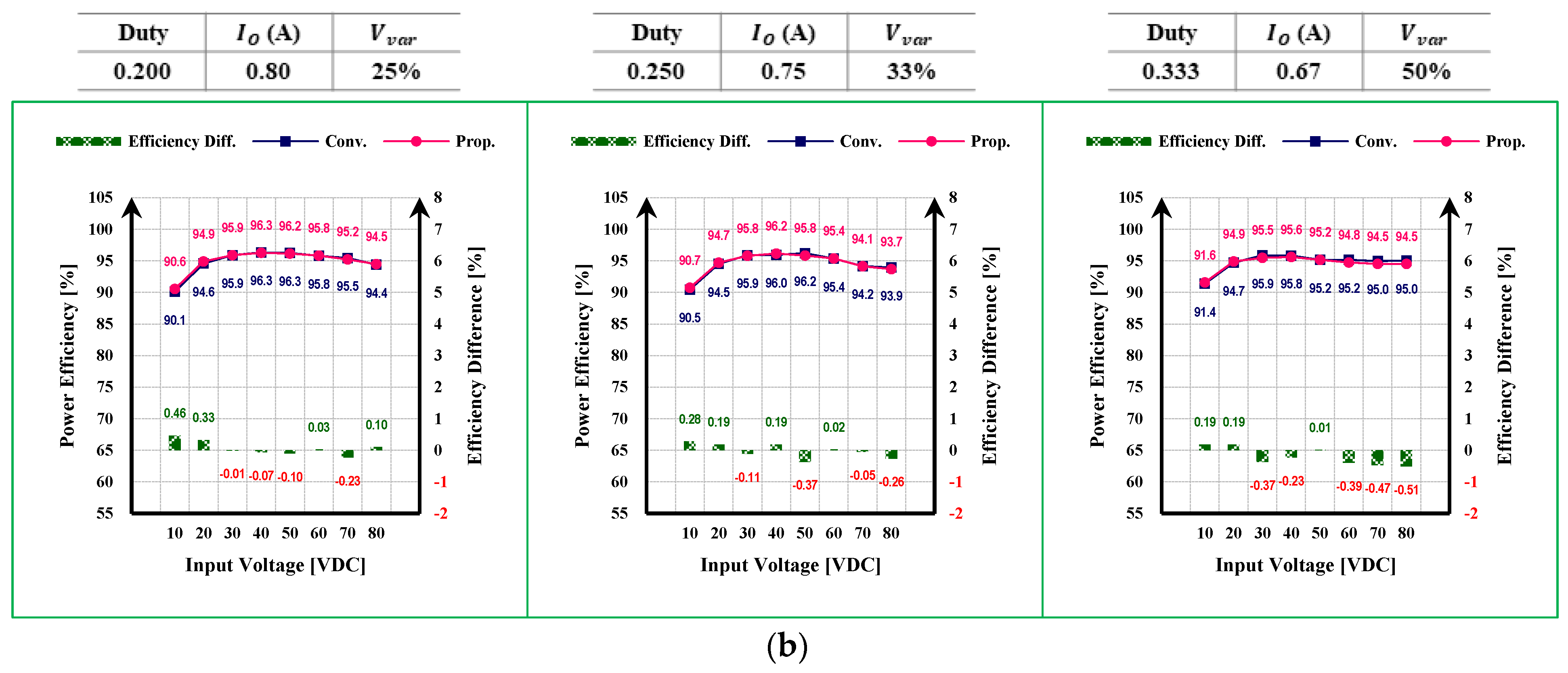
5.3.1. Step-Down
Figure 11 shows the power efficiency in the step-down section of the buck-boost topology in the CV and CC modes. The power efficiency is improved in every condition because of the removal of D
2 in the switch-off section. In the CV mode, the efficiency improvement becomes larger with an increase in the output current;
increases in the high-power region. In the CC mode, the power efficiency improves with a decrease in the input voltage, and
increases in the low-power region. In the same duty condition, the voltage stress of the diode D
1 increases with the input voltage;
decreases with an increase in loss.
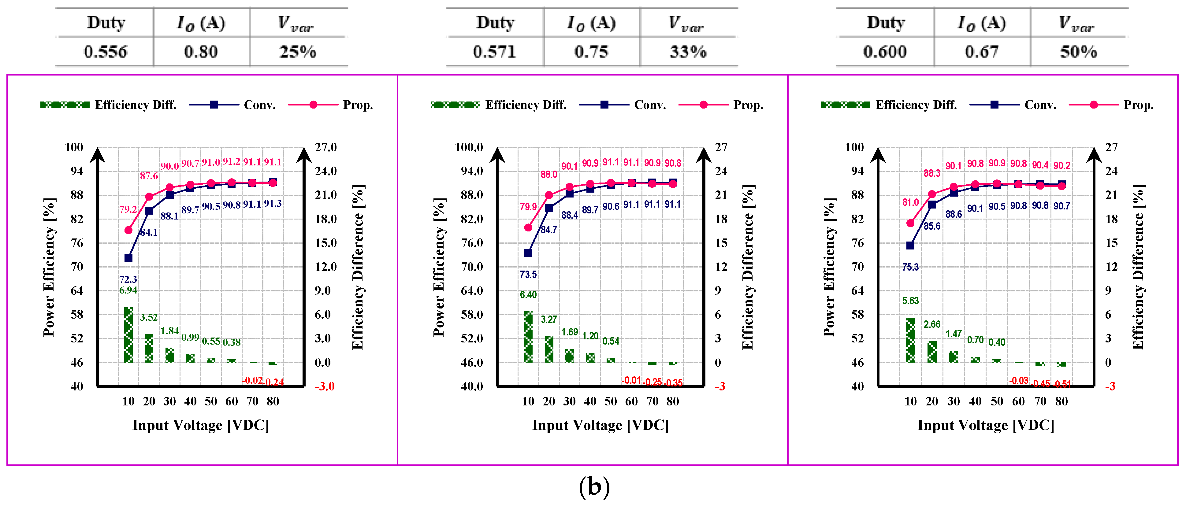
5.3.2. Step-Up
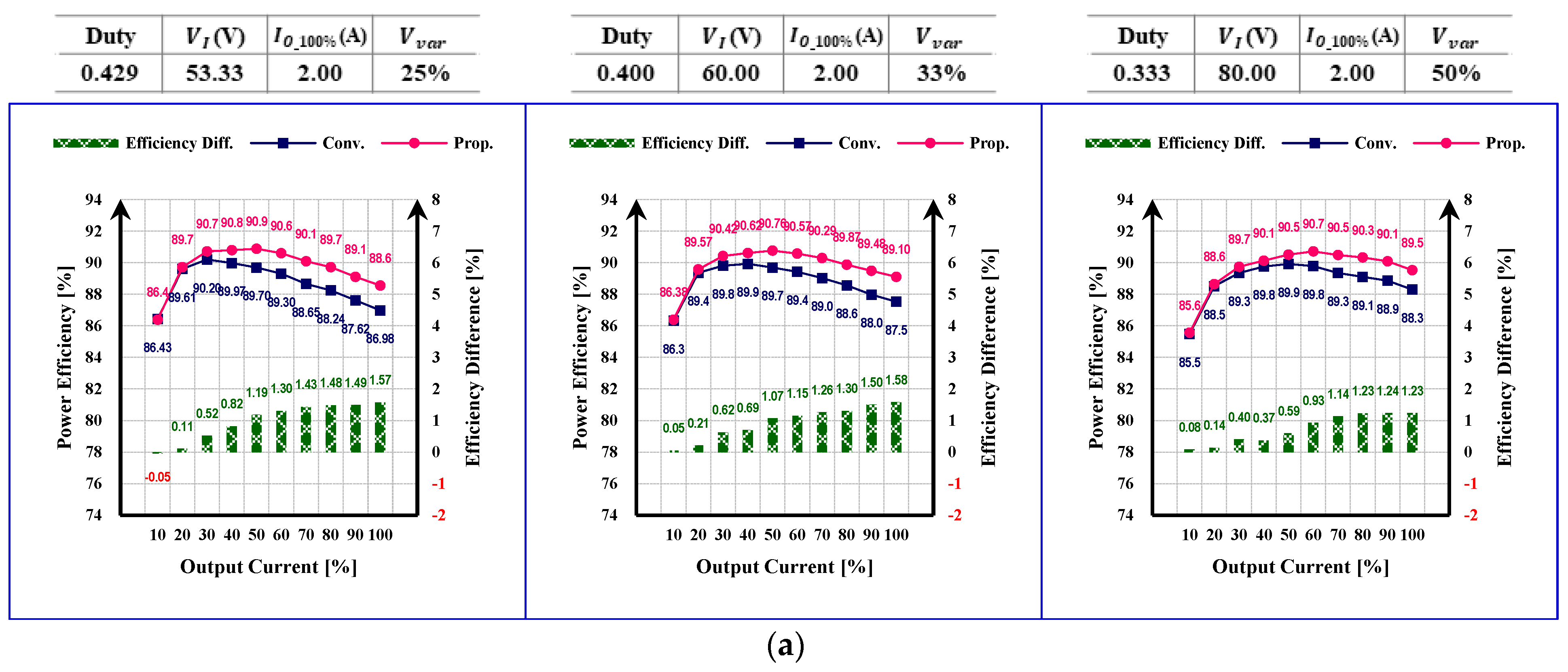
Figure 12 shows the power efficiency of the step-up buck-boost topology in the CV and CC modes. In the CV mode, the efficiency improves in general to 10–80 W and
increases in the high-power region where the output current increases. In the CC mode,
decreases with an increase in
and the input voltage. The power efficiency decreases more than the conventional converter at a power of 50 W or higher. In the step-up section, the output voltage increases with the input voltage, and the voltage stress of diode D
1 also increases. The efficiency decreases more than the conventional converter because the resulting diode loss exceeds the increase in the efficiency obtained by the removal of D
2 in the switch-off section. Therefore, the proposed converter is suitable for applications below 50 W in the step-up section of the buck-boost topology.
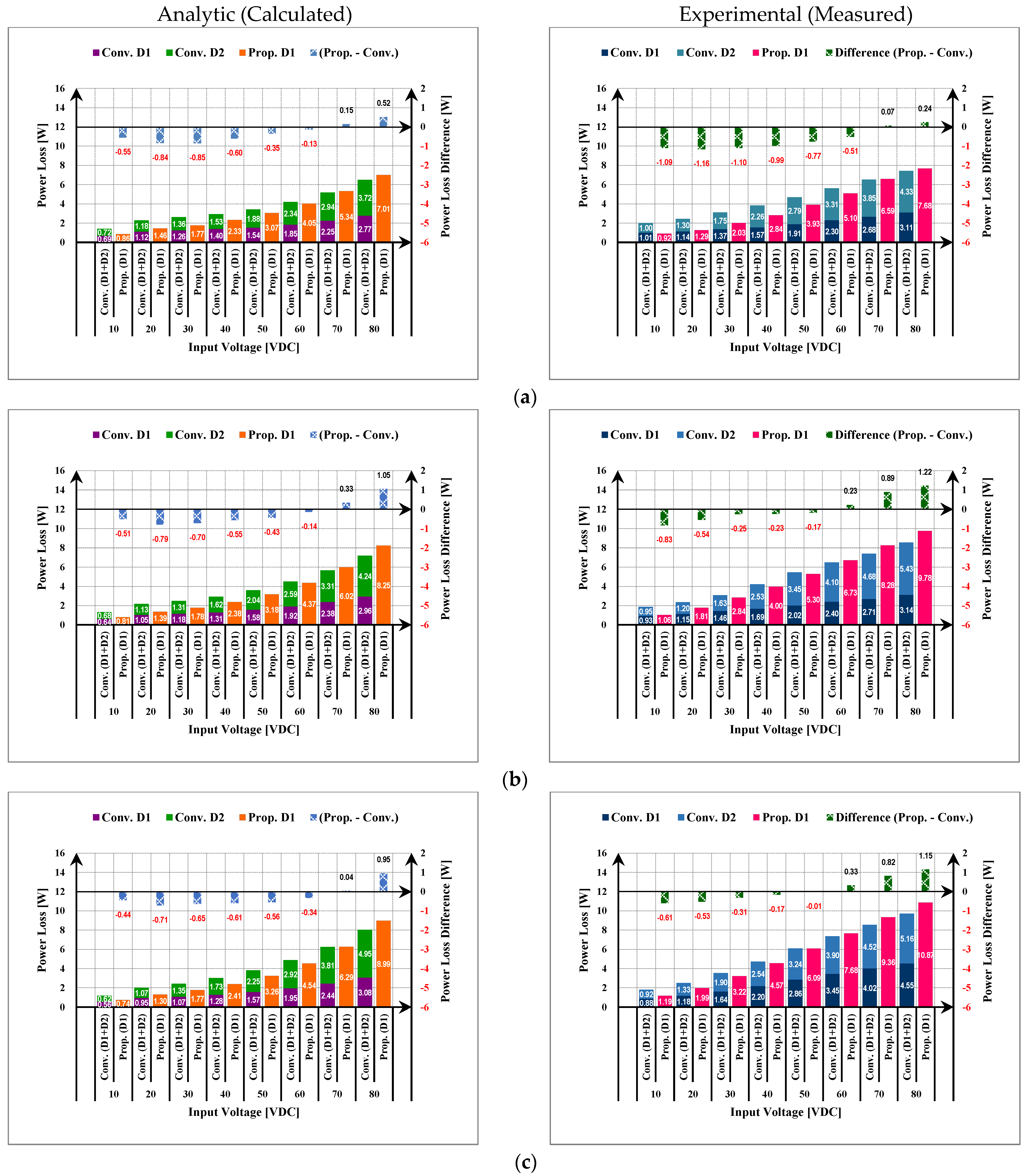
5.3.3. Diode Stress (Buck-Boost Step-Up, CC Mode)
Figure 13 shows the analytic and experimental diode power loss in the CC mode in the step-up section of the buck-boost topology. A positive power loss difference
implies that the diode loss of the proposed TSBB converter is large, whereas if it is negative, it implies a large diode loss of the conventional TSBB converter.
To calculate the diode loss, information on several parameters was referenced from the datasheet and all data are typical values at 25 degrees. Parameters not provided in the datasheet were used to calculate the diode loss with some assumptions.
Forward voltage : obtained from the VF-IF characteristic curve.
Equivalent resistance : obtained from the VF-IF characteristic curve by linear approximation under the current conditions used in the experiment.
Reverse recovery time and peak reverse recovery current : estimated and calculated using value 16 nsec at the forward current = 1.0 A and the reverse current = 0.5 A.
Peak reverse recovery voltage : assumed at and corrected coefficient by temperature with VR characteristic curve.
Ignored any other parasitic factors like internal inductance, capacitance, and so on.
Due to several assumptions and uncertain parameter values, the two results are slightly different. This is expected to be due to the reverse recovery characteristics that change exponentially with the increase in temperature and voltage stress, and also to be affected by parasitic components on the PCB and errors in measurement equipment.
Despite these differences, both results show a similar trend in which diode losses rapidly increase with voltage stress over a certain region, thereby diode power loss of the proposed TSBB converter is bigger than the conventional converter over a certain input voltage. The increase in the D1 loss of the proposed TSBB converter becomes larger than the power efficiency improvement by the removal of D2. The power efficiency is reversed at the point where the difference in diode loss changes from negative to positive (+). For the proposed TSBB converter, the power efficiency increases at 60 W or lower at the duty ratio of 0.556; the power efficiency increases at 50 W or lower at the duty ratios of 0.571 and 0.600.
6. Conclusions
This study proposed a modified design of the TSBB converter to improve power efficiency using fewer conduction components and measured the optimal output power range. The proposed TSBB converter improved power efficiency in buck and buck-boost topologies by reducing the conduction loss caused by the diode in the switch-off section power efficiency. A 100 W prototype was designed and fabricated to verify the improvement. Experiments were conducted in the CV/CC modes of three topologies, and the power efficiency was measured for 10–80 W. In the buck topology, power efficiency improved in the entire power range of 10–80 W; it increased on average by 0.75–1.36% and 0.83–2.27% in the CV and CC modes, respectively. In the buck-boost topology step-down, the power efficiency improved in the entire power range of 10–80 W; it improved on average by 0.73–0.99% and 3.33–4.75% in the CV and CC modes, respectively. In the buck-boost topology step-up, the power efficiency increased on average by 1.65–2.00% in the entire power range of 10–80 W in the CV mode, and by 2.17–2.77% in the power range of the 10–50 W in the CC mode.
In future research, we will study how to reduce the conduction and switching losses by reducing the voltage and current stress of semiconductors for efficiency improvement. In addition, we will analyze the effect on output ripple under various conditions by using inductance, capacitance, and switching frequency as design variables, and study how these parameters affect converter efficiency.


