
Fabrication of the Cu2ZnSnS4 Thin Film Solar Cell via a Photo-Sintering Technique

 ,
,
Abstract
:1. Introduction
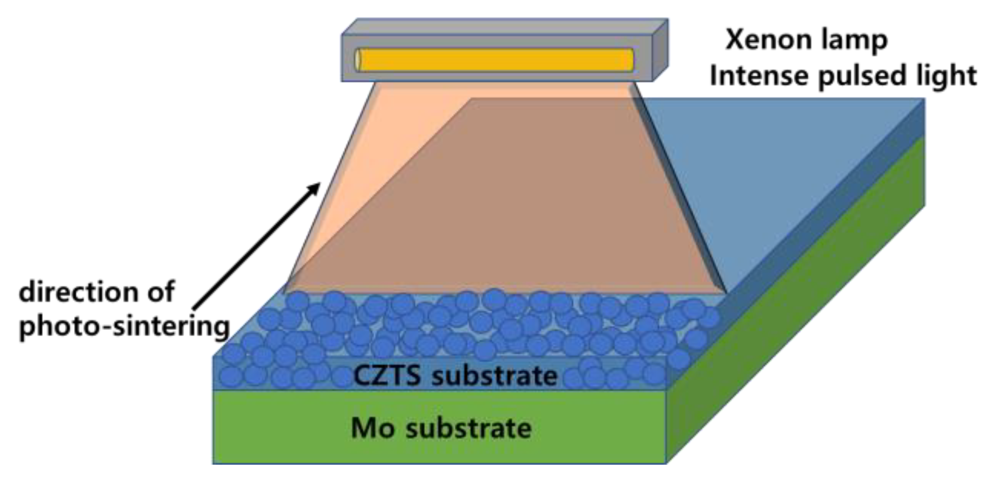
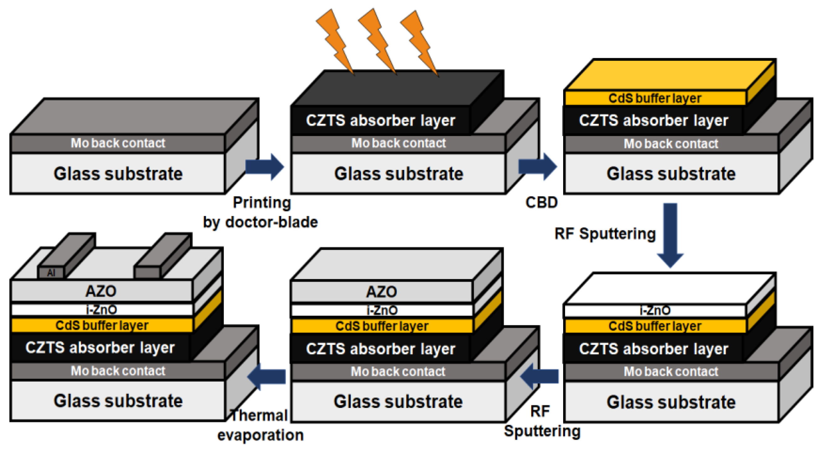
2. Materials and Methods
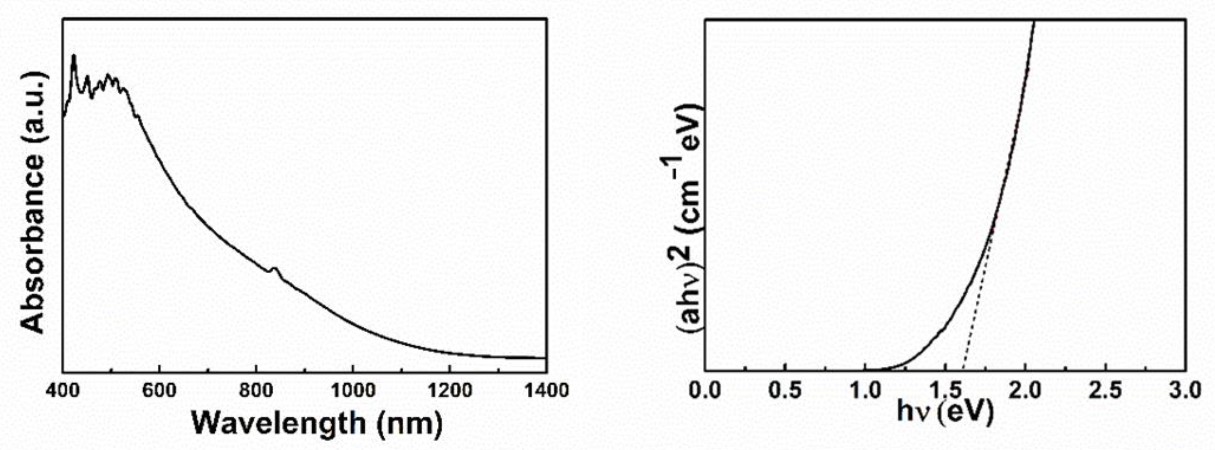
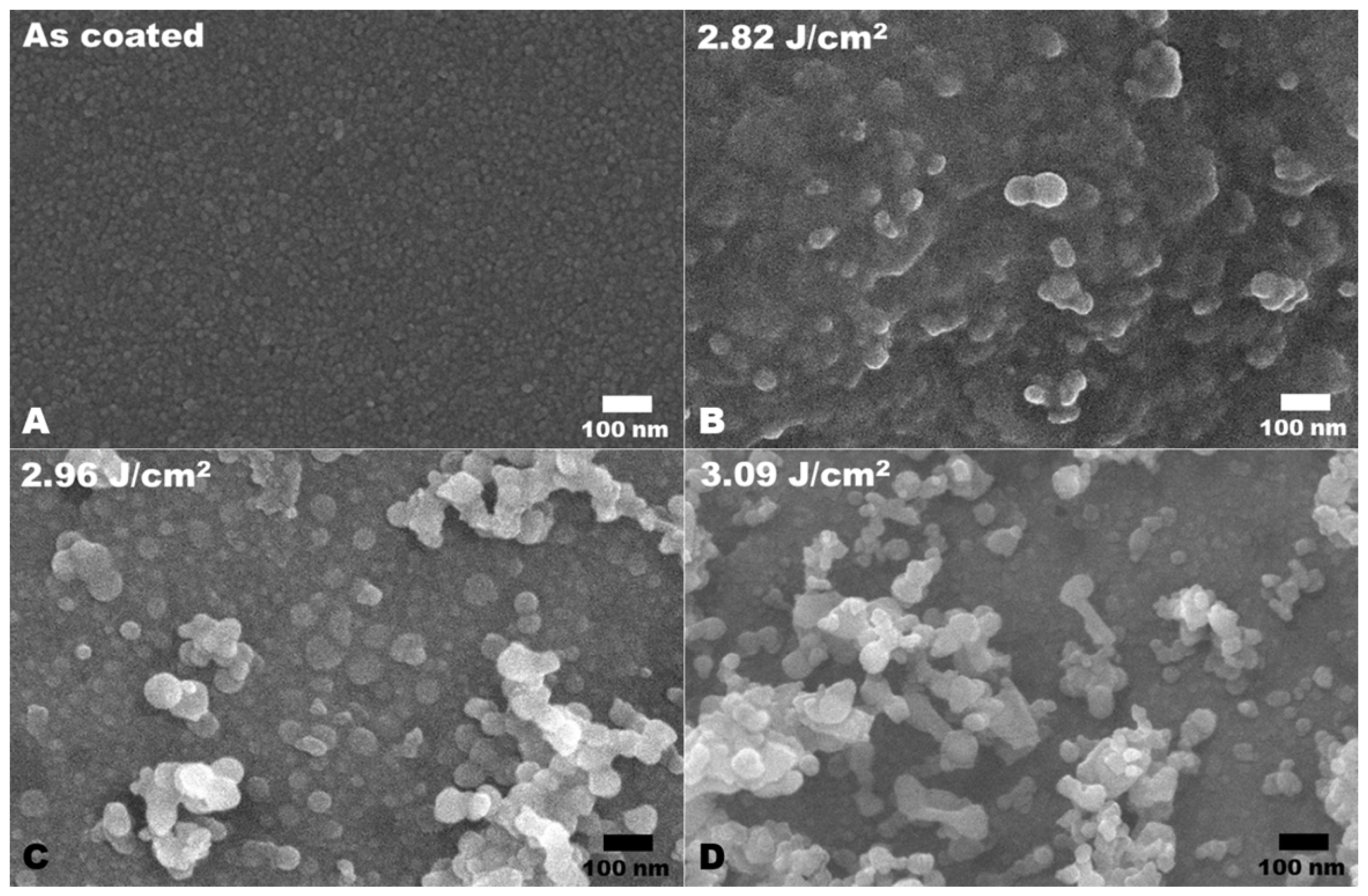
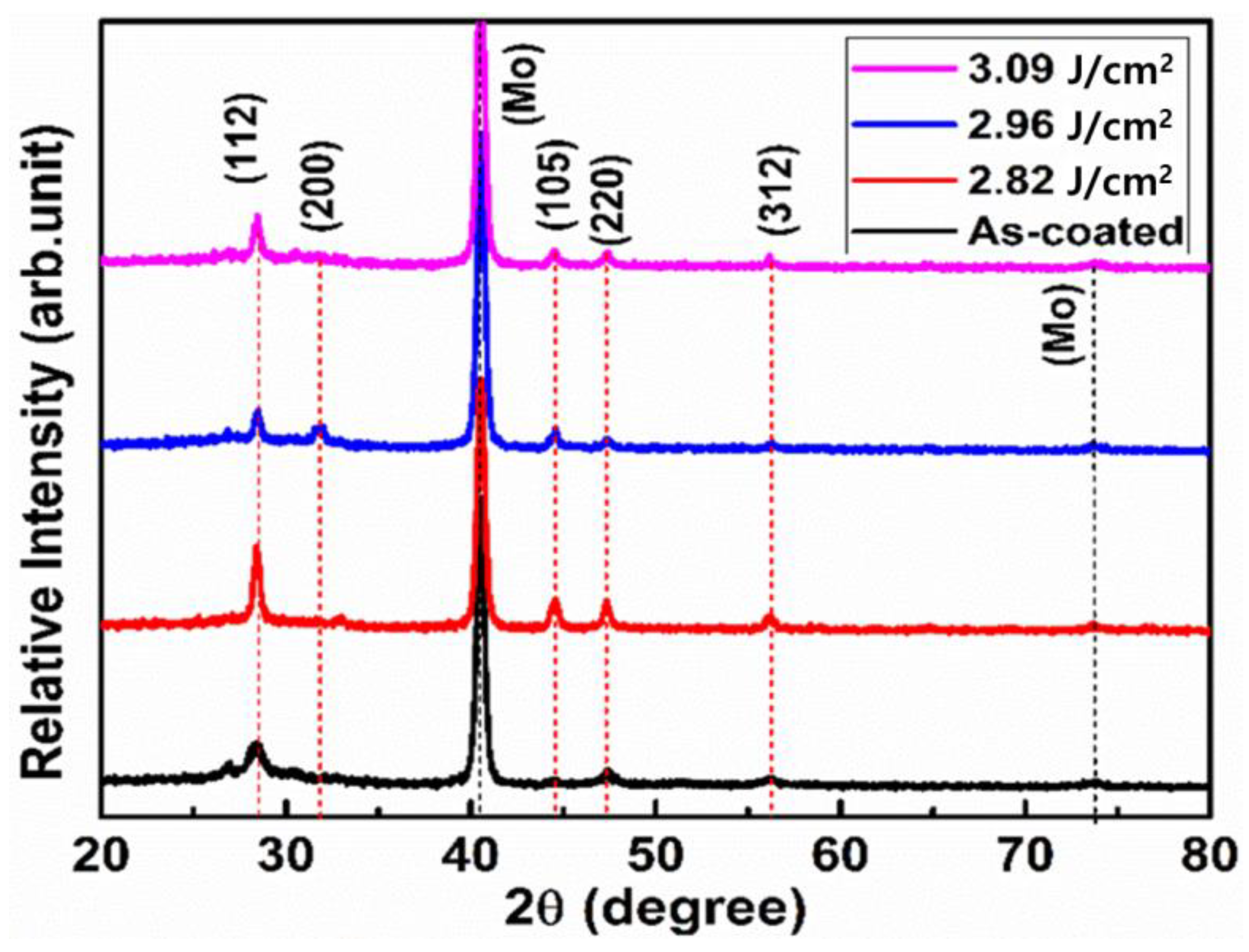
3. Results and Discussion
4. Conclusions
Author Contributions
Funding
Institutional Review Board Statement
Informed Consent Statement
Data Availability Statement
Conflicts of Interest
References
- Mukesh, K.; Ashish, D.; Nirmal, A.; Swaminathan, V.; Qiao, Q. Strategic review of secondary phases, defects and defect-complexes in kesterite CZTS–Se solar cells. Energy Environ. Sci. 2015, 8, 3134–3159. [Google Scholar]
- Wei, W.; Mark, T.W.; Oki, G.; Tayfun, G.; Teodor, K.T.; Yu, Z.; David, B.M. Device Characteristics of CZTSSe Thin-Film Solar Cells with 12.6% Efficiency. Adv. Energy Mater. 2013, 4, 1301465. [Google Scholar]
- Krishan, P.; Pawan, S.; Abhishikta, B.; Kenm, B.T. Current challenges and future prospects for a highly efficient (>20%) kesterite CZTS solar cell: A review. Sol. Energy Mater Sol. Cells. 2019, 196, 138–156. [Google Scholar]
- Swati, T.; Sadanand; Pooja, L.; Dilip, K.D. Contribution to sustainable and environmental friendly non-toxic CZTS solar cell with an innovative hybrid buffer layer. Sol. Energy 2020, 204, 748–760. [Google Scholar]
- Liu, X.; Feng, Y.; Cui, H.; Liu, F.; Hao, X.; Conibeer, G.; Mitzi, D.B.; Green, M. The current status and future prospects of kesterite solar cells: A brief review. Prog. Photovoltaics. 2016, 24, 879–898. [Google Scholar] [CrossRef]
- Andrew, F.; Eric, G.; Victor, I.; Xavier, F.; Fabian, A.P.; Osvaldo, V.; Alejandro, P.; Edgardo, S. Development of a Selective Chemical Etch to Improve the Conversion Efficiency of Zn-Rich Cu2ZnSnS4 Solar Cells. JACS 2012, 134, 8018–8021. [Google Scholar]
- Michael, P.; Leo, C.; Alain, L.; Catherine, G.; Stephane, J. Solid-State NMR and Raman Spectroscopy to Address the Local Structure of Defects and the Tricky Issue of the Cu/Zn Disorder in Cu-Poor, Zn-Rich CZTS Materials. Inorg. Chem. 2014, 53, 8646–8653. [Google Scholar]
- Liu, W.; Chen, S.; Huang, C.; Lee, M.; Kuo, H. Investigation of Zn/Sn ratio for improving the material quality of CZTS thin films with the reduction of Cu2-xS secondary phase. J. Alloys. Compd. 2021, 853, 157237. [Google Scholar] [CrossRef]
- Lund, E.A.; Du, H.; Hlaing, W.M.; Teeter, G.; Scarpulla, M.A. Investigation of combinatorial coevaporated thin film Cu2ZnSnS4 (II): Beneficial cation arrangement in Cu-rich growth. J. Appl. Phys. 2014, 115, 173503. [Google Scholar] [CrossRef]
- Pratikshya, S.; Noah, H.; Peter, H.P.; Bin, L.; Viktor, C. Size-Controlled Synthesis of Iron and Iron Oxide Nanoparticles by the Rapid Inductive Heating Method. ACS Omega 2020, 5, 19853–19860. [Google Scholar]
- Uma, G.; Mahesh, S.; Seung, W.S.; Kishor, G.; Pramod, P.; Sambhaji, P.; Chang, W.H.; Jin, H.K.; Sanjay, K. Towards environmentally benign approaches for the synthesis of CZTSSe nanocrystals by a hot injection method: A status review. Chem. Commun. 2014, 50, 11258–11273. [Google Scholar]
- Han, J.; Fu, G.; Krishnakumar, V.; Liao, C.; Wolfram, J. CdS annealing treatments in various atmospheres and effects on performances of CdTe/CdS solar cells. J. Mater. Sci. Mater. Electron. 2013, 77, 2695–2700. [Google Scholar]
- Hulya, M.G.; Ramazan, E. Annealing studies on CBD grown CdS thin films. J. Cryst. Growth 2003, 258, 141–148. [Google Scholar]
- Chung, Y.; Cho, D.; Park, N.; Lee, K.; Kim, J. Effect of annealing on CdS/Cu(In,Ga)Se2 thin-film solar cells. Curr. Appl. Phys. 2011, 11, S65–S67. [Google Scholar] [CrossRef]
- Dharmadasa, R.; Lavery, B.W.; Dharmadasa, I.; Druffel, T. Processing of CdTe thin films by intense pulsed light in the presence of CdCl2. J. Coat. Technol. Res. 2015, 12, 835–842. [Google Scholar] [CrossRef]
- Thad, D.; Ruvini, D.; Brandon, W.L.; Krishnamraju, A. Intense pulsed light processing for photovoltaic manufacturing. Sol. Energy Mater. Sol. Cells 2018, 174, 359–369. [Google Scholar]
- Sonali, D.; Kadambinee, S.; Prakash, M.; Jagatpati, R.; Injamul, A.; Ramagouri, S.; Pitamber, M. Synthesis of quaternary chalcogenide CZTS nanoparticles by a hydrothermal route. IOP Conf. Ser. Mater. Sci. Eng. 2018, 10, 674–677. [Google Scholar]
- Vu, M.H.C.; Soohyun, H.; Jian, L.; Jaehyeong, L. Performance of Cu(In, Ga)Se2 Solar Cells on Zinc Sulfide Buffer Layers for Various Power Values of an Intense Pulsed Light System. JNN 2019, 19, 1635–1639. [Google Scholar]
- Cao, V.M.H.; Hwang, S.; Lin, J.; Lee, S.; Kim, S.; Lee, J. Effects of Photosintering on Properties of Cadmium Sulfide Thin Films for Highly Efficient Cu(In, Ga)(Se, S)2 Solar Cells. SAM 2018, 10, 1133–1139. [Google Scholar] [CrossRef]
- Sekou, M.C.; Lingling, W.; Xintong, Z. Easy hydrothermal preparation of Cu2ZnSnS4 (CZTS) nanoparticles for solar cell application. Nanotech 2013, 24, 495401. [Google Scholar]
- Katy, H.; Bonna, K.N.; Jeffrey, L.J.; Hui, D.; Paulo, A.F.; Vardaan, C.; Trudy, B.; Bruce, M.C.; Antonio, F.C.; Glenn, T.; et al. Detection of ZnS phases in CZTS thin-films by EXAFS. In Proceedings of the IEEE 37th Photovoltaic Specialist Conference (PVSC), Seattle, WA, USA, 19–24 June 2011. [Google Scholar]
- Ali, A.; Moiz, M.; Kamarulazizi, I.; Muhammad, A.F. Effect of sulfurization time on the properties of copper zinc tin sulfide thin films grown by electrochemical deposition. Sci. Rep. 2016, 6, 32431. [Google Scholar]
- Hironori, K.; Kazuo, J.; Win, S.M.; Koichiro, O.; Makoto, Y.; Hideaki, A.; Akiko, T. Development of CZTS-based thin film solar cells. Thin Solid Films. 2009, 517, 2455–2460. [Google Scholar]
- Jonathan, J.S.; Phillip, J.D.; Laurence, M.P. Towards sustainable materials for solar energy conversion: Preparation and photoelectrochemical characterization of Cu2ZnSnS4. Electrochem. Commun. 2008, 10, 639–642. [Google Scholar]
- Caleb, K.M.; Wei-Chang, Y.; Charles, J.H.; Nathaniel, J.C.; Chinmay, S.J.; Eric, A.S.; Rakesh, A. 9.0% efficient Cu2ZnSn(S,Se)4 solar cells from selenized nanoparticle inks. Prog. Photovoltaics. 2014, 23, 654–659. [Google Scholar]
- Kim, K.; Pan, C.; Bansal, S.; Malhotra, R.; Kimd, D.; Chang, C. Scalably synthesized environmentally benign, aqueous-based binary nanoparticle inks for Cu2ZnSn(S,Se)4 photovoltaic cells achieving over 9% efficiency. Sustain. Energy Fuels. 2017, 1, 267–274. [Google Scholar] [CrossRef]
- Wang, W.; Han, S.; Sung, S.; Kim, D.; Chang, C. 8.01% CuInGaSe2 solar cells fabricated by air-stable low-cost inks. Phys. Chem. Chem. Phys. 2012, 14, 11154–11159. [Google Scholar] [CrossRef]
- Liu, J.; Zhuang, D.; Luan, H.; Cao, M.; Xie, M.; Li, X. Preparation of Cu(In,Ga)Se2 thin film by sputtering from Cu(In,Ga)Se2 quaternary target. Prog. Nat. Sci. 2013, 23, 133–138. [Google Scholar] [CrossRef] [Green Version]
- Zhang, P.; Yu, Q.; Min, X.; Guo, L.; Shi, J.; Zhao, X.; Li, D.; Luo, Y.; Wu, H.; Meng, Q.; et al. Fabrication of Cu2ZnSn(S,Se)4 photovoltaic devices with 10% efficiency by optimizing the annealing temperature of precursor films. RSC Adv. 2018, 8, 4119–4124. [Google Scholar] [CrossRef] [Green Version]


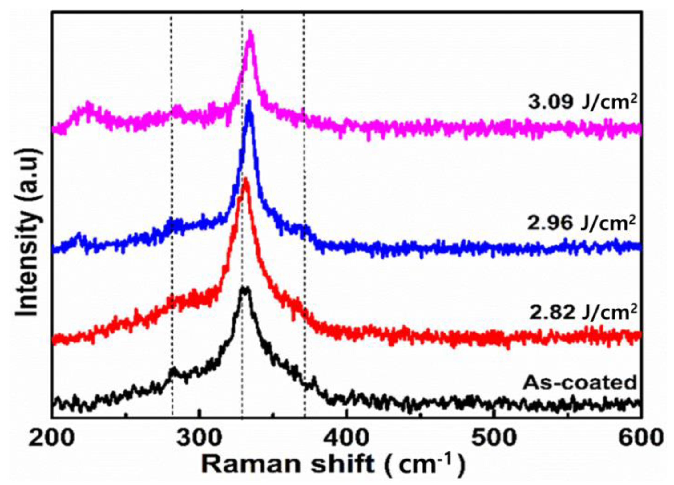
| Condition | Peak (cm−1) | FWHM |
|---|---|---|
| As-coated | 329.281 | 28.837 |
| 2.82 J/cm2 | 331.307 | 22.333 |
| 2.96 J/cm2 | 333.838 | 13.642 |
| 3.09 J/cm2 | 334.345 | 13.318 |
| Treatment Condition | Elemental Component (at%) | Composition Ratio (at%) | ||||||
|---|---|---|---|---|---|---|---|---|
| S | Sn | Cu | Zn | Cu/(Zn + Sn) | Zn/Sn | Cu/Sn | S/Metal | |
| As-coated | 47.35 | 25.56 | 17.77 | 9.32 | 0.943 | 1.906 | 2.742 | 0.899 |
| 2.82 J/cm2 | 47.88 | 24.7 | 16.24 | 11.18 | 0.900 | 1.452 | 2.209 | 0.918 |
| 2.96 J/cm2 | 46.46 | 24.66 | 17.88 | 11.01 | 0.853 | 1.623 | 2.239 | 0.867 |
| 3.09 J/cm2 | 47.54 | 23.01 | 16.98 | 12.46 | 0.781 | 1.362 | 1.846 | 0.906 |
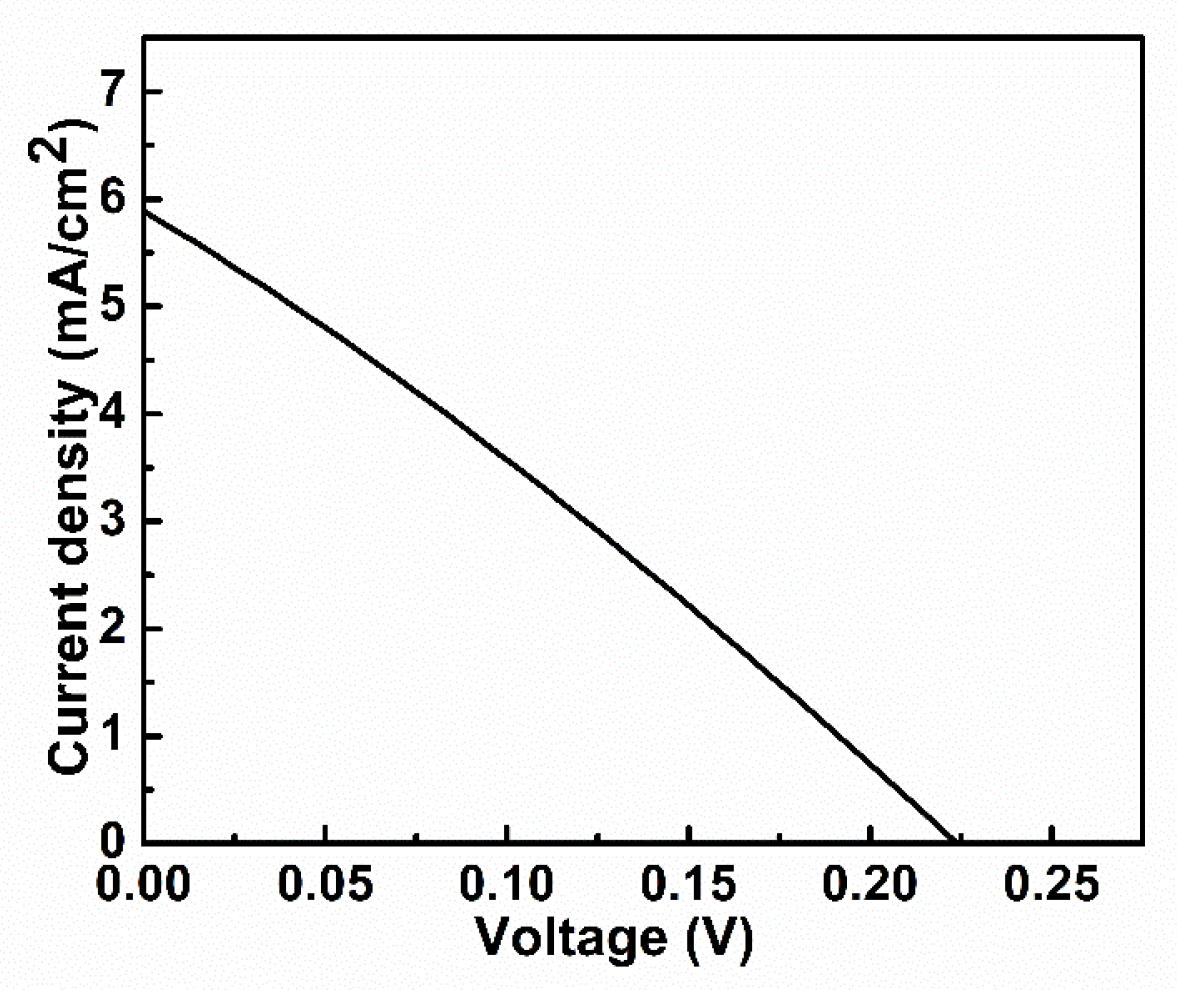
| Condition | Voc (V) | Isc (mA/cm2) | Fill Factor (%) | Efficiency (%) | Rsh (Ω) | Rs (Ω•cm2) |
|---|---|---|---|---|---|---|
| 2.96 J/cm2 | 0.224 | 5.913 | 32.789 | 1.01 | 378.713 | 26.417 |
Publisher’s Note: MDPI stays neutral with regard to jurisdictional claims in published maps and institutional affiliations. |
© 2021 by the authors. Licensee MDPI, Basel, Switzerland. This article is an open access article distributed under the terms and conditions of the Creative Commons Attribution (CC BY) license (https://creativecommons.org/licenses/by/4.0/).
Share and Cite
Cao, V.M.H.; Bae, J.; Shim, J.; Hong, B.; Jee, H.; Lee, J. Fabrication of the Cu2ZnSnS4 Thin Film Solar Cell via a Photo-Sintering Technique. Appl. Sci. 2022, 12, 38. https://doi.org/10.3390/app12010038
Cao VMH, Bae J, Shim J, Hong B, Jee H, Lee J. Fabrication of the Cu2ZnSnS4 Thin Film Solar Cell via a Photo-Sintering Technique. Applied Sciences. 2022; 12(1):38. https://doi.org/10.3390/app12010038
Chicago/Turabian StyleCao, Vu Minh Han, Jaesung Bae, Joongpyo Shim, Byungyou Hong, Hongsub Jee, and Jaehyeong Lee. 2022. "Fabrication of the Cu2ZnSnS4 Thin Film Solar Cell via a Photo-Sintering Technique" Applied Sciences 12, no. 1: 38. https://doi.org/10.3390/app12010038