Article

Generalized Structures for Switched-Capacitor Multilevel Inverter Topology for Energy Storage System Application

1
Department of Electrical Engineering, Aligarh Muslim University, Aligarh 202002, India
2
Industrial Engineering Department, College of Engineering, King Saud University, P.O. Box 800, Riyadh 11421, Saudi Arabia
3
Department of Statistics and Operations Research, College of Science, King Saud University, P.O. Box 2455, Riyadh 11451, Saudi Arabia
*
Author to whom correspondence should be addressed.
Appl. Sci. 2021, 11(3), 1319; https://doi.org/10.3390/app11031319
Submission received: 24 October 2020 / Revised: 15 January 2021 / Accepted: 25 January 2021 / Published: 1 February 2021
(This article belongs to the Special Issue Power Electronic Applications in Power and Energy Systems)

Abstract

:
The apparent advantages of Multilevel Inverter (MLI) topologies in handling medium and high power with less loss in switching and lower harmonic distortion in an output voltage waveform makes it better than the conventional inverter. However, the MLI topologies utilize a large number of DC power supplies and power semiconductor devices. They also have a higher value of total standing voltage (TSV). Moreover, capacitor voltage balancing problems, self-voltage boosting inability, and complex control techniques require a relook and improvement in their structure. More recently, Switched-Capacitor Multilevel Inverter (SCMLI) topologies have been proposed to overcome the shortcomings of MLIs. In this paper, a generalized structure for a single-phase switched capacitor multilevel inverter (SCMLI) with self-voltage boosting and self-voltage balancing capability is proposed. A detailed analysis of a general structure of SCMLI is presented. The comparative analysis of the structures is carried out with recently reported topologies to demonstrate superiority. An optimized low-frequency modulation controls the output voltage waveform. The simulation and experimental results are included in the paper for single-unit symmetric (9-level voltage) and asymmetric (17-level voltage) configurations.

1. Introduction

Nowadays, the alteration of power from DC to AC is an important process and performs a vital task in modern power system network and industrial processes powered by electric drives [1]. DC to AC conversion is carried out by power electronics converters. Due to high harmonic losses in two-level inverters, multilevel inverters are used in order to have highly efficient power electronics and drive systems [2]. The main property of the Multilevel Inverter (MLI) is to generate an output voltage waveform resembling a staircase using several voltage sources at the input, which results in the low value of total harmonics distortion (THD) and minimal values of electromagnetic interference (EMI) and voltage stress across switches [3]. The three classical topologies of MLI are Cascaded H-bridge inverter (CHB), Flying Capacitor Clamped inverter (FC), and Neutral Point Clamped inverter (NPC) [4]. Due to easy control and unique characteristics, they are practically implemented as alteration technology in various applications ranging from small- to large-scale industries. In order to achieve higher voltage levels, a large number of devices are required, which enhances the size and cost of MLIs [5]. At higher voltage levels, NPC and FC show capacitor voltage unbalancing problems besides the requirement for a significant number of clamping diodes and capacitors, respectively [6]. Cascaded H-bridge is the most feasible and flexible among the conventional topologies, utilizing less components, but the requirement of high DC power supply is a shortcoming, which makes MLI bulky and costly. Further, the classical topologies also do not have the ability to boost the output voltage [7]. Many symmetric topologies with less switches have been presented by the authors of [8,9,10,11,12] to overcome the problem of large switch requirements. However, as voltage levels increase considerably, DC power supplies, power semiconductor devices, gate driver circuits, and capacitors required in the topology increases. To overcome this drawback, reduced device count asymmetric topologies are used, which have DC power supplies of different magnitudes. In [13,14,15,16,17,18,19,20], various reduced device count asymmetric topologies have been presented. Both reduced device count symmetric as well as asymmetric topologies presented in [8,9,10,11,12,13,14,15,16,17,18,19,20] suffer from a self-voltage boosting inability and the capacitor voltage unbalancing problem due to which these topologies are not suitable for low-input DC voltage source applications. Some auxiliary circuits such as impedance network or forehead-type boost converter are used along with MLI to achieve a self-voltage boosting capability [21]. To overcome the problem of capacitor voltage unbalancing, a complex control algorithm was proposed in [22,23]. However, the cost, size, and complexity in the control mechanism are enhanced.
To overcome MLI’s shortcomings, a Switched-capacitor Multilevel Inverter (SCMLI) has recently been proposed by various researchers. SCMLIs require fewer switches and driver circuits compared to other existing topologies, and they need less DC power supplies because capacitors act as alternate DC sources. The idea of SCMLIs was first proposed by O.C. Mak and A. Ioinovici in 1998 [24]. In [25], an integrated switched-capacitor MLI topology with a voltage string was presented, which needed a low number of switches, but it suffered from high voltage stress across the backend switch H-Bridge. To overcome this problem, the author of [26] presented an improved integrated switched-capacitor MLI topology. The author of [27] proposed an SCMLI topology using a series-parallel conversion, and it can be extended to generate a high number of voltage levels. However, it requires a significant number of components at high voltage levels. A novel stepup SCMLI topology developed by the author of [28] includes a switched capacitor DC/DC converter (SCC) and a full-bridge. SCC and full-bridge are used as a level generator and polarity generator, respectively. To further increase the number of output voltage levels with a reduced number of devices, the authors of [29] presented an SCMLI topology. However, the topologies presented in [28,29] have high voltage stress across H- bridge switches due to which it cannot be used in high voltage applications except medium voltage applications. Moreover, the per-unit total standing voltage (TSV) in both topologies is high. Self-balanced step-up SCMLI topologies were presented in [30,31] to overcome these problems. Thus, there is a requirement for a generalized structure of SCMLI, which can be used to obtain the desired number of voltage levels. In this paper, a generalized SCMLI topology structure was proposed with the target being reduced power electronic switches, driver circuits, capacitors and reduced TSV per unit for a higher number of voltage levels. This paper is organized as follows: Section 2 discusses the detailed analysis of the proposed generalized structure. In Section 3, the generalized SCMLI topology structures are compared with recently proposed topologies. In Section 4, an analysis of the basic unit is presented. The simulation results are discussed and its experimental validation are presented in Section 5. The paper is concluded in Section 6.

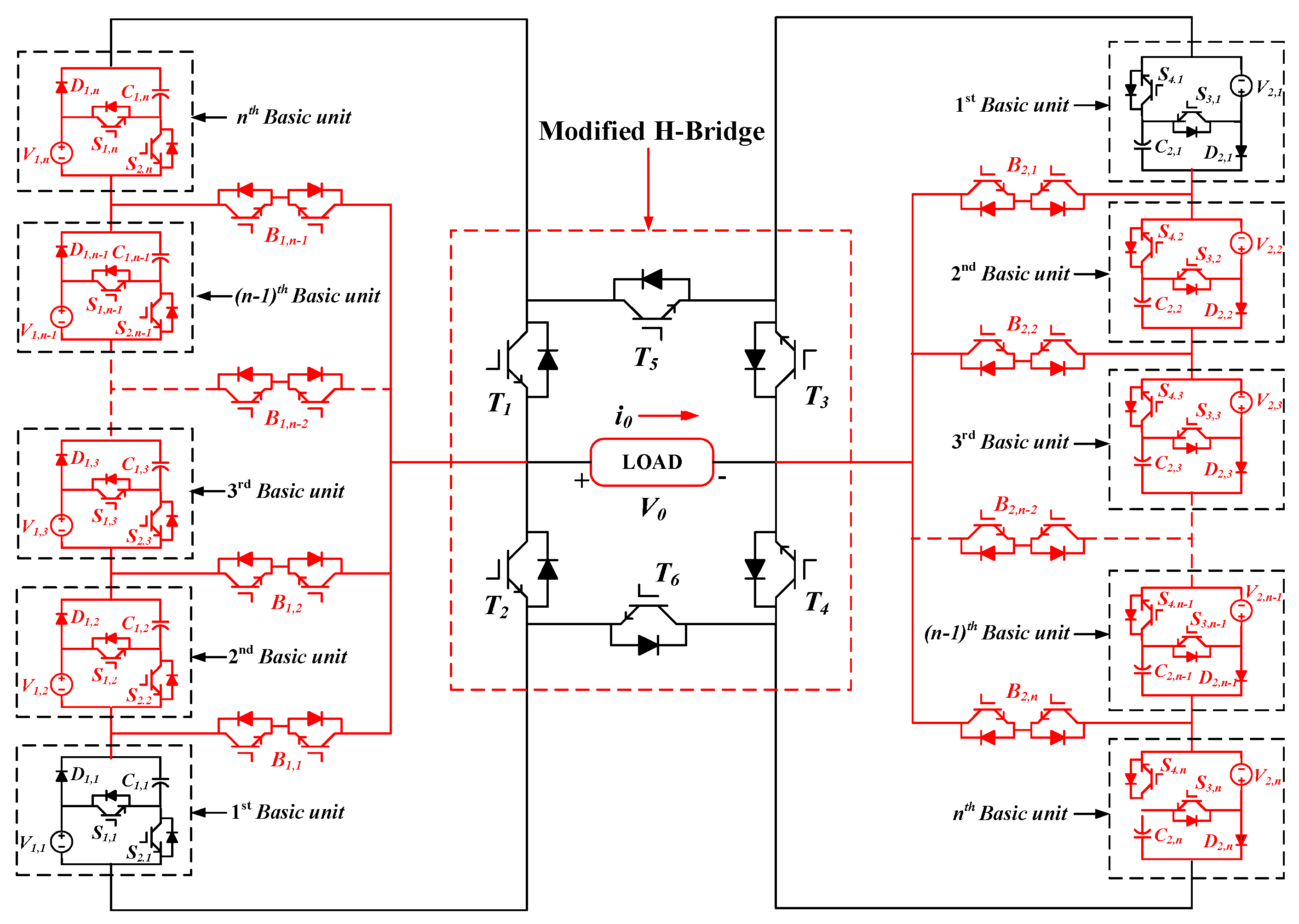
2. Proposed Generalized Structures of the Switched Capacitor Multilevel Inverter

A generalized structure of MLI (GSMLI) has been proposed in this paper. It is shown in Figure 1. It is obtained by extending the modified H-bridge inverter on the left and on both sides.
GSMLI: The GSMLI is achieved by including (n − 1) basic units and (n − 1) bidirectional switches (B1,1, B1,2, ……, B1,n−1) to each side of the modified H-bridge, as shown in Figure 1 in red. Therefore, there are 2n total basic units from which n basic units are connected to the left side of the modified H-bridge and the remaining n basic units are on the right side of the bridge.
GSMLI can be operated in two different methods depending on the magnitude of the DC voltage sources of the left-side basic units.
(a) First method (GSMLI.1): When the basic units 1st, 2nd, 3rd, …, nth unit connected to the left side of the modified H-bridge have an equal magnitude of DC voltage sources and the basic units 1st, 2nd, 3rd, …, nth unit connected to the right side of the modified H-bridge have an equal magnitude of DC voltage sources but different from the left side basic units:
V1,1 = V1,2 = V1,3 = ……….V1,n−1 = V1,n = V
Then, to generate the maximum possible voltage levels in this condition, the following equation must be satisfied by the voltage sources of basic units connected to the right side:
V2,1 = V2,2 = V2,3 = ……….V2,n−1 = V2,n = (2n + 1)V
The capacitors C1,1, C1,2, C1,3, …, C1,n−1, C1,n are charged to V through switches S2,1, S2,2, S2,3, …, S2,n−1, S2,n, respectively, and switches S1,1, S1,2, S1,3, …, S1,n−1, S1,n are used for discharging the capacitors. The capacitors C2,1, C2,2, C2,3, …, C2,n−1, C2,n are charged to (2n + 1)V through switches S4,1, S4,2, S4,3, …, S4,n−1, S4,n, respectively, and switches S3,1, S3,2, S3,3, …, S3,n−1, S3,n are used for discharging the capacitors.
The maximum value of the blocked voltage across switches excluding bidirectional switches B1,1, B1,2, …, B1,n−1 and B2,1, B2,2, …, B2,n−1 are given as
VSi,1 = VSi,2 = VSi,3 =……….VSi,n−1 = VSi,n = V, i = 1,2
VSi,1 = VSi,2 = VSi,3 =……….VSi,n−1 = VSi,n = (2n + 1)V, i = 3,4
VT1 = VT2 = 2nV, VT3 = VT4 = 2n(2n + 1)V
VT5 = VT6 = 4n(4n + 1)V
The maximum value of the blocked voltage across diodes D1,1, D1,2, …, D1,n−1, and D2,1, D2,2, …, D2,n−1 are given as
VD1,1 = VD1,2 = VD1,3 = ……….VD1,n−1 = VD1,n = V
VD2,1 = VD2,2 = VD2,3 = ……….VD2,n−1 = VD2,n = (2n + 1)V
The maximum value of the blocked voltage across bidirectional switches B1,1, B1,2, …, B1,n−1 are given as follows:
When n is odd
V B 1 , i   =   ( 2 n   2 i ) V   for   i   =   1 ,   2 ,   3 , . n 1 2   for   n   2
V B 1 , j   =   2 j V   for   j   =   n 1 2   +   1 ,   n 1 2   +   2 , n 1   for   n   2
When n is even
V B 1 , i   =   ( 2 n   2 i ) V   for   i   =   1 ,   2 ,   3 , . n 2 2   for   n   2
V B 1 , j   =   2 j V   for   j   =   n 2 2   +   1 ,   n 2 2 + 2 , n 1   for   n   2
The maximum value of blocked voltage across bidirectional switches B2,1, B2,2, …, B2,n−1) are given as follows:
When n is odd
V B 2 , i   =   ( 2 n 2 i ) ( 2 n + 1 ) V   for   i   =   1 ,   2 , . n 1 2   for   n   2
V B 2 , j   =   2 ( 2 n + 1 ) V for   j   =   n 1 2   +   1 ,   n 1 2 + 2 , n 1   for   n   2
When n is even
V B 2 , i   =   ( 2 n 2 i ) ( 2 n + 1 ) V   for   i   =   1 ,   2 , . n 2 2   for   n   2
V B 2 , j   =   2 j ( 2 n + 1 ) V   for   j   =   n 2 2   +   1 ,   n 2 2   +   2 , n 1   for   n   2
TSVB1 of bidirectional switches B1,1, B1,2, …, B1,n−1 is given as follows:
When n is odd
TSV B 1   =   i = 1 n 1 2 ( 2 n 2 i ) V   + j = n 1 2 + 1 n 1 ( 2 j ) V for   n   2
TSV B 1   =   [ 3 n 2 4 n + 1 2 ] V for   n   2
When n is even
TSV B 1   =   i = 1 n 1 2 ( 2 n 2 i ) V   +   j = n 1 2 + 2 n 2 ( 2 j ) V   +   n for n   2
TSV B 1   =   [ 3 n 2 6 n 2 ] V for   n   2
TSVB2 of bidirectional switches B2,1, B2,2, …, B2,n−1) is given as follows:
When n is odd
TSV B 2   =   i = 1 n 1 2 ( 2 n 2 i ) ( 2 n + 1 ) V   +   j = n 1 2 + 1 n 1 ( 2 j ) ( 2 n + 1 ) V for   n   2
TSV B 2   =   [ 3 n 2 4 n + 1 2 ] ( 2 n + 1 ) V for   n   2
When n is even
TSV B 2   =   i = 1 n 1 2 ( 2 n 2 i ) V   + j = n 1 2 + 2 n 2 ( 2 j ) V   +   n for   n   2
TSV B 2   =   [ 3 n 2 6 n 2 ] ( 2 n + 1 ) V for   n   2
Therefore, TSV of the proposed GSMLI.1 is given as
T S V   =   ( i = 1 n V S 1 , i )   +   ( i = 1 n V S 2 , i )   +   ( i = 1 n V S 3 , i )   +   ( i = 1 n V S 4 , i )   +   ( i = 1 n V D 1 , i )   +   ( i = 1 n V D 2 , i )   +   ( i = 1 6 V T i )   +   TSV B 1   +   TSV B 2
T S V   =   =   [ 6 n 3 + 90 n 2 + 38 n + 2 2 ] V for   odd   values   of   n   2
T S V   =   =   [ 6 n 3 + 82 n 2 + 32 n 2 ] V for   even   values   of   n   2
TSV in per unit of the proposed GSMLI.1 is given as
T S V p . u   =   [ 6 n 3 + 90 n 2 + 38 n + 2 8 n 2 + 8 n ]   for   odd   values   of   n 2
T S V p . u .   =   [ 6 n 3 + 82 n 2 + 32 n 8 n 2 + 8 n ]   for   even   values   of   n   2
(b) Second method (GSMLI.2): When the basic units 1st, 2nd, 3rd, …, nth unit connected to each side of the modified H-bridge have an unequal magnitude of DC voltage sources and generate the maximum possible voltage levels, the voltage magnitude of DC sources must be selected in a binary fashion as given by the following relation:
V 1 , j   =   2 j 1 V   for   j   =   1 , 2 , 3 , , n
V 2 , j   =   2 j 1 . ( 2 n + 1 1 ) V   for   j   =   1 , 2 , 3 , , n
The capacitors C1,1, C1,2, C1,3, …, C1,n−1, C1,n and capacitors C2,1, C2,2, C2,3, …, C2,n−1, C2,n are charged in binary fashion. The voltage across capacitors C1,1, C1,2, C1,3, …, C1,n−1, C1,n are given by the following equation:
V C 1 , j   =   2 j 1 V   for   j   =   1 , 2 , 3 , , n
The voltage across capacitors C2,1, C2,2, C2,3, …, C2,n−1, C2,n are given as
V C 2 , j   =   2 j 1 . ( 2 n + 1 1 ) V   for   j   =   1 , 2 , 3 , , n
The maximum value of the blocked voltage across switches excluding bidirectional switches B1,1, B1,2, …, B1,n−1 are given as
V S 1 , j   =   V S 2 , j   =   2 j 1 V   for   j   =   1 , 2 , 3 , , n
V S 3 , j   =   V S 4 , j   =   2 j 1 . ( 2 n + 1 1 ) V   for   j   =   1 , 2 , 3 , , n
V T 1 =   V T 2 =   ( 2 n + 1 2 ) V ,   V T 3 =   V T 4 =   ( 2 n + 1 2 ) ( 2 n + 1 1 ) V
V T 5 =   V T 6 =   ( 2 n + 1 2 )   ( 2 n + 1 ) V
The maximum value of the blocked voltage across diodes D1,1, D1,2, …, D1,n−1, and D2,1, D2,2, …, D2,n−1 are given as
V D 1 , j   =   2 j 1 V   for   j   =   1 , 2 , 3 , , n
V D 2 , j   =   2 j 1 . ( 2 n + 1 1 ) V   for   j   =   1 , 2 , 3 , , n
The maximum value of the blocked voltage across bidirectional switches B1,1, B1,2, …, B1,n−1 are given as
V B 1 , j   =   ( 2 n + 1 2 2 i = 1 j 2 i 1 ) V for   n     2
The maximum value of the blocked voltage across bidirectional switches B2,1, B2,2, …, B2,n−1 are given as
V B 1 , j   =   ( 2 n + 1 2 2 i = 1 j 2 i 1 ) ( 2 n + 1 1 ) V for   n     2
TSVB1 of the bidirectional switches B1,1, B1,2, …, B1,n−1 is given as
T S V B 1   =   [ ( n 2 ) 2 n + 1   +   4 ] V   for   n     2
TSVB2 of the bidirectional switches B2,1, B2,2, …, B2,n−1 is given as
T S V B 2   =   [ ( n 2 ) 2 n + 1 + 4 ] ( 2 n + 1 1 ) V   for   n     2
The overall TSV of the proposed GSMLI.2 is given as
T S V   =   [ ( 2 n 9 ) 2 n   +   2 2 n + 3   +   1 ] ( 2 n + 1 ) V   for   n     2
TSV in per unit of the proposed GSMLI.2 is given as
T S V p . u   =   [ [ ( 2 n 9 ) 2 n + 2 2 n + 3 + 1 ] 2 n + 1 2 ]   for   n   2
For n number of basic units connected to each side of the modified H-bridge, the numbers of levels (NL), switches (Nsw), driver circuits (Ndri), diodes (Ndiode), and capacitors (Ncap) in terms of the number of stages (n) and the number of level (NL) for GSMLI.1 and GSMLI.2 are given by Table 1.

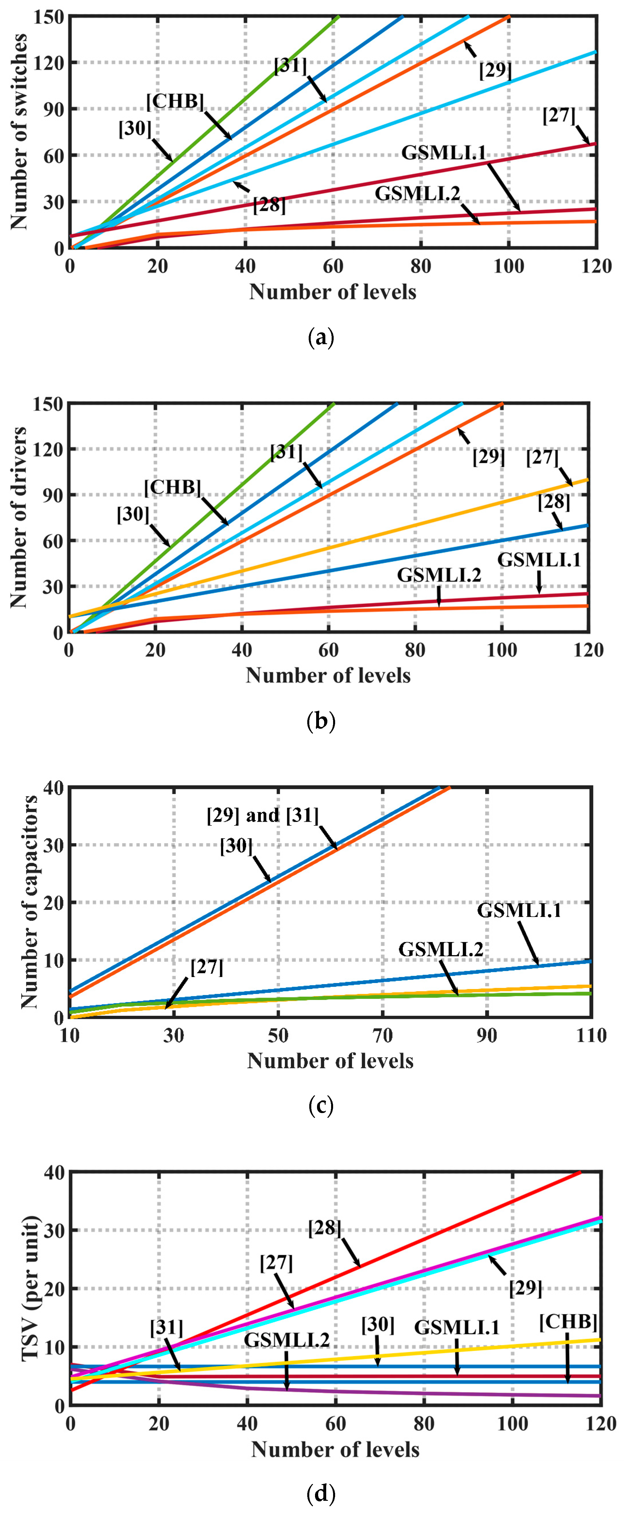
3. Comparative Analysis of the Proposed GSMLI Topology

The proposed generalized structure was compared with other recent topologies. The performance of various parameters such as numbers of diodes (Ndiode), switches (Nsw), capacitors (Ncap), drivers (Ndri), and TSVp.u., and cost function per level (CF/NL), are shown in Figure 2. It may be noted that all these topologies are designed to generate seventeen levels of output voltage. Cost function per level (CF/NL) is defined as
CF = (Nsw + Ncap + Ndri + Ndiode + α*TSV) × Nsource
Here, α represents the contribution of TSV in the cost function
The comparisons are carried out among the levels of generalized structure of the proposed topology and other topologies. The comparison is conducted in terms of numbers of switches, drivers, capacitors, diodes, and TSV when all generated the same levels. From Figure 2a, it can be observed that the number of switches required in the generalized structure in both methods (first and second) is less than the number of switches required by other topologies for the same number of levels. It can also be seen from Figure 2a that the number of switches required in the second method generalized structure is less than the switches required by the first method of generalized structure. From Figure 2b,c, it is clear that the number of driver circuits and capacitors required in GSMLI in both methods (first and second) is less than the number of drivers and capacitors required by other topologies for the same number of levels. In [28], there is no capacitor, which is why it is not shown in Figure 2c.
From Figure 2d, it is clear that the TSV (in per unit) in GSMLI (second method) is less than the other topologies when all generated the same number of levels. TSV (in per unit) in the GSMLI (first method) is higher than the CHB and in [30] when all generated the same number of levels; however, it requires less switches, drivers, and capacitors compared to CHB and in [30].

4. Analysis of the Basic Unit of GSMLI

The generalized topology presented in this work was simulated and experimentally verified by considering one unit in symmetric and asymmetric mode. It has also been tested for TSV, and optimal capacitance was calculated in this section. The basic units act as a level generator that can produce two voltage levels from a solitary DC power supply. Figure 3 shows the conducting paths of the proposed topology for asymmetric configuration. Switches S2 and S4 and diodes D1 and D2 of the basic units are utilized for the charging purpose of capacitors C1 and C2, respectively, while switches S1 and S3 are used for discharging capacitors C1 and C2, respectively, in order to take the participation of the capacitor voltages into consideration in voltage level generation. The switches used in the modified H-Bridge are T1, T2, T3, T4, T5, and T6. Positive voltage levels are generated by utilizing switches T1, T4, and T6, whereas negative voltage levels are generated by utilizing switches T2, T3, and T5. Thus, the operation of switch pairs (T1, T2), (T3, T4), (T5, T6), (T7, T8), (S1, S2), and (S3, S4) are complementary. This topology is capable of generating 0V, ±V1, ±(V1 + VC1), ±V2, ±(V1 + V2), ±(V1 + VC1 + V2), ±(V2 + VC2), ±(V1 + V2 + VC2), and ±(V1 + VC1 + V2 + VC2) voltage levels. This topology is self-balancing for capacitor voltage because charging and discharging take place in an alternate manner and, if there is any voltage drop in capacitors voltage due to discharging, then it is regained during charging. This topology can damp out the disparate voltage between the capacitor and power supply, due to which it acts as a practically effective power circuit.

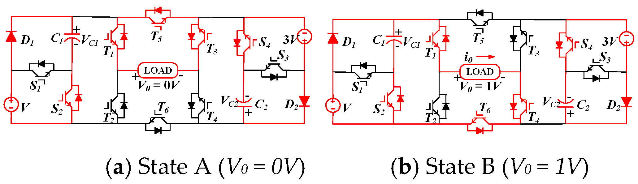
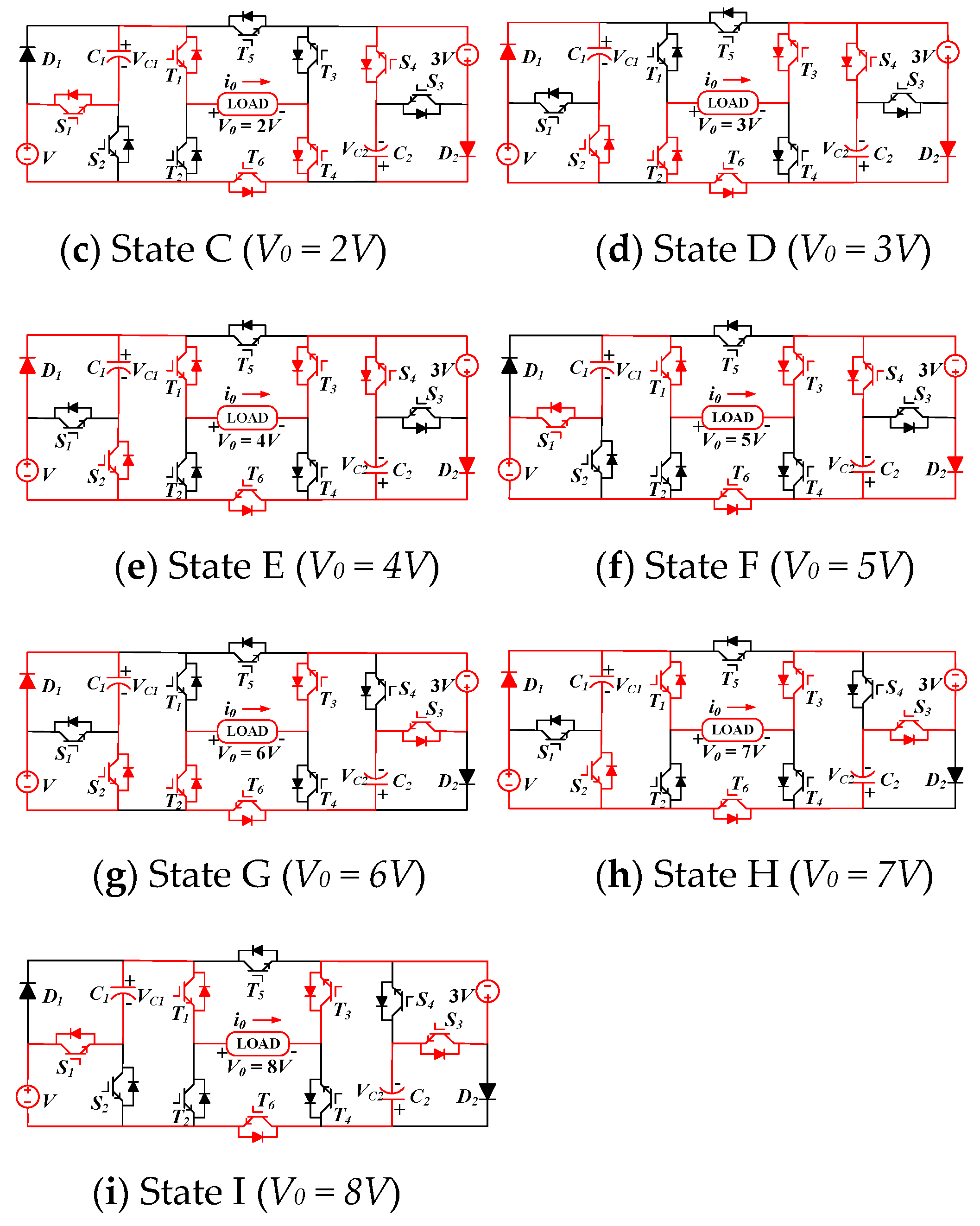
4.1. Operating States

The proposed topology can be utilized in asymmetric and symmetric configurations. Table 2 illustrates the switching states of T1 to T6 and S1 to S4, the charging and discharging states of capacitors C1 and C2 in a fastidious switching state. “C” and “D” indicate that the capacitor is charged and discharged, respectively. “-” indicates that there is no change in the states of the capacitors. “1” denotes the on state of switches, while “0” denotes the off state of switches.
When both DC voltage sources have the same magnitude (V1 = V2), then it is operated in symmetric configuration and produces 9 levels in 0V, ± V1, ± (V1 + VC1), ± (2V1 + VC1), and ± (2V1 + VC1 + VC2) output voltage waveform, which can be seen from Table 2. From Table 2, it can be observed that more levels are generated when both voltage sources have different magnitudes of voltage, i.e., asymmetric configuration.
To generate the maximum available voltage levels, it must be operated in asymmetric configuration and the magnitude of DC voltage sources V1 and V2 must be selected in a 1:3 ratio. When it is operated in asymmetric configuration (3V1 = V2), it produces 17 levels (0V, ± V1, ± (V1 + VC1), ± 3V1, ± 4V1, ± (4V1 + VC1), ± (3V1 + VC2), ± (4V1 + VC2), and ± (4V1 + VC1 + VC2)) in output voltage waveform, as shown in Table 2.
Total standing voltage (TSV) is one of the most important parameters while designing different inverter topologies. TSV is defined as the sum of the maximum blocked voltage (stress) across the semiconductor switches and diodes when the output voltage of all possible levels is generated at the output.
The maximum value of blocked voltage across each switch in symmetric configuration (V1 = V2 = V) is given as
VT1 = VT2 = 2V1 = 2V, VT3 = VT4 = 2V2 = 2V
VT5 = VT6 = 2(V1+V2) = 4V, VS1 = VS2 = V1 = V
VS3 = VS4 = V2 = V, VD1 = V1 = V, VD2 = V2 = V
where VT1, VT2, VT3, VT4, VT5, VT6, VS1, VS2, VS3, VS4, VD1, andVD2 are the blocked voltages across switches T1, T2, T3, T4, T5, T6, S1, S2, S3, and S4 respectively.
TSV = VT1 + VT2 + VT3 + VT4 + VT5 + VT6 + VS1 + VS2 + VD1 + VS3 + VD2 + VS4 = 22V
TSV in per unit is defined as
T S V p . u .   =   T S V V o , m a x
where Vo,max is the maximum value of output voltage
TSVp.u in symmetric configuration is given as
T S V p . u .   =   22 V 4 V   =   5.5
The maximum value of the blocked voltage across each switch in asymmetric configuration (V1 = V and V2 = 3V) is given as
VT1 = VT2 = 2V1 = 2V, VT3 = VT4 = 2V2 = 6V
VT5 = VT6 = 2(V1+V2) = 8V, VS1 = VS2 = V1 = V
VS3 = VS4 = V2 = 3V, VD1 = V1 = V, VD2 = V2 = 3V
TSV = 44V
TSVp.u in asymmetric configuration is given as
T S V p . u .   =   44 V 8 V   =   5.5

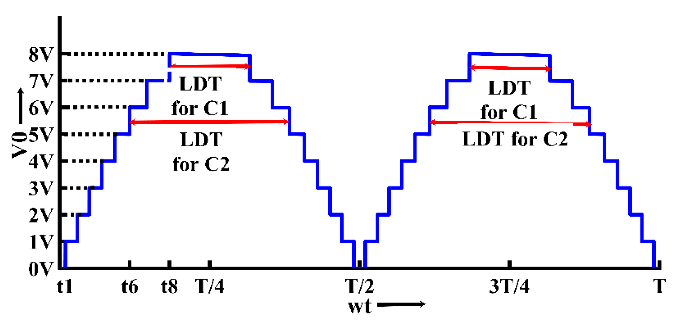
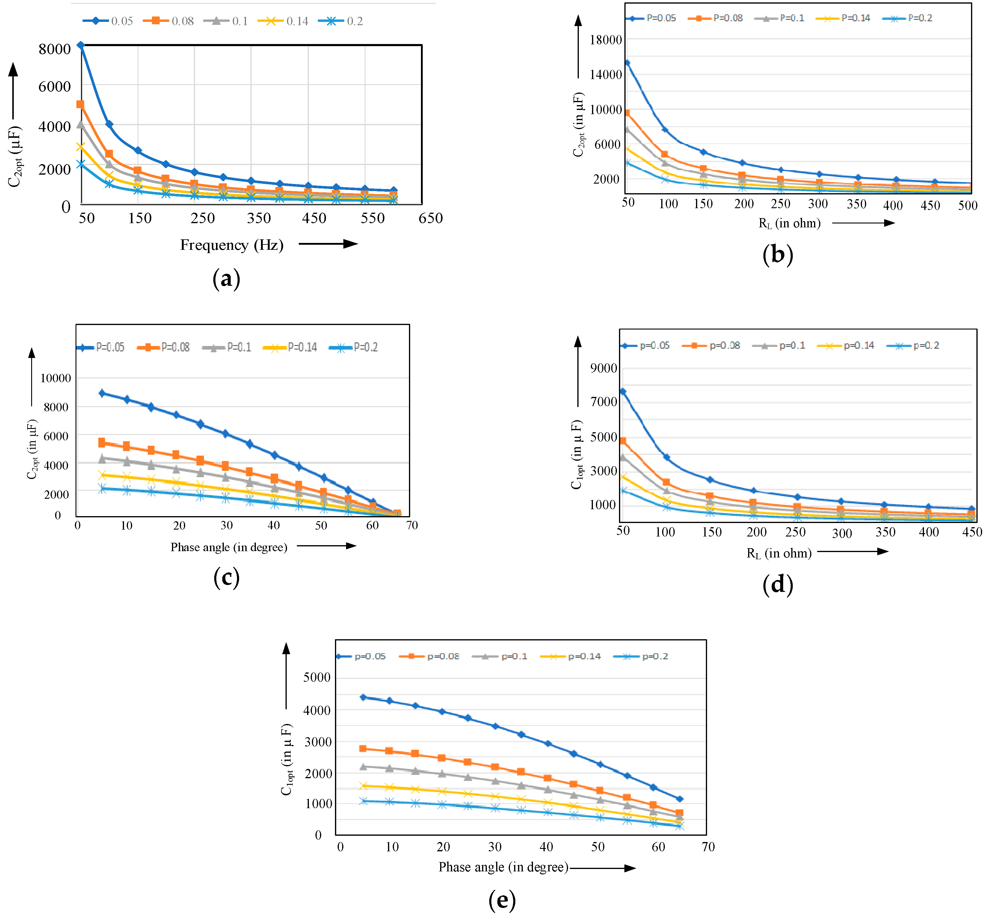
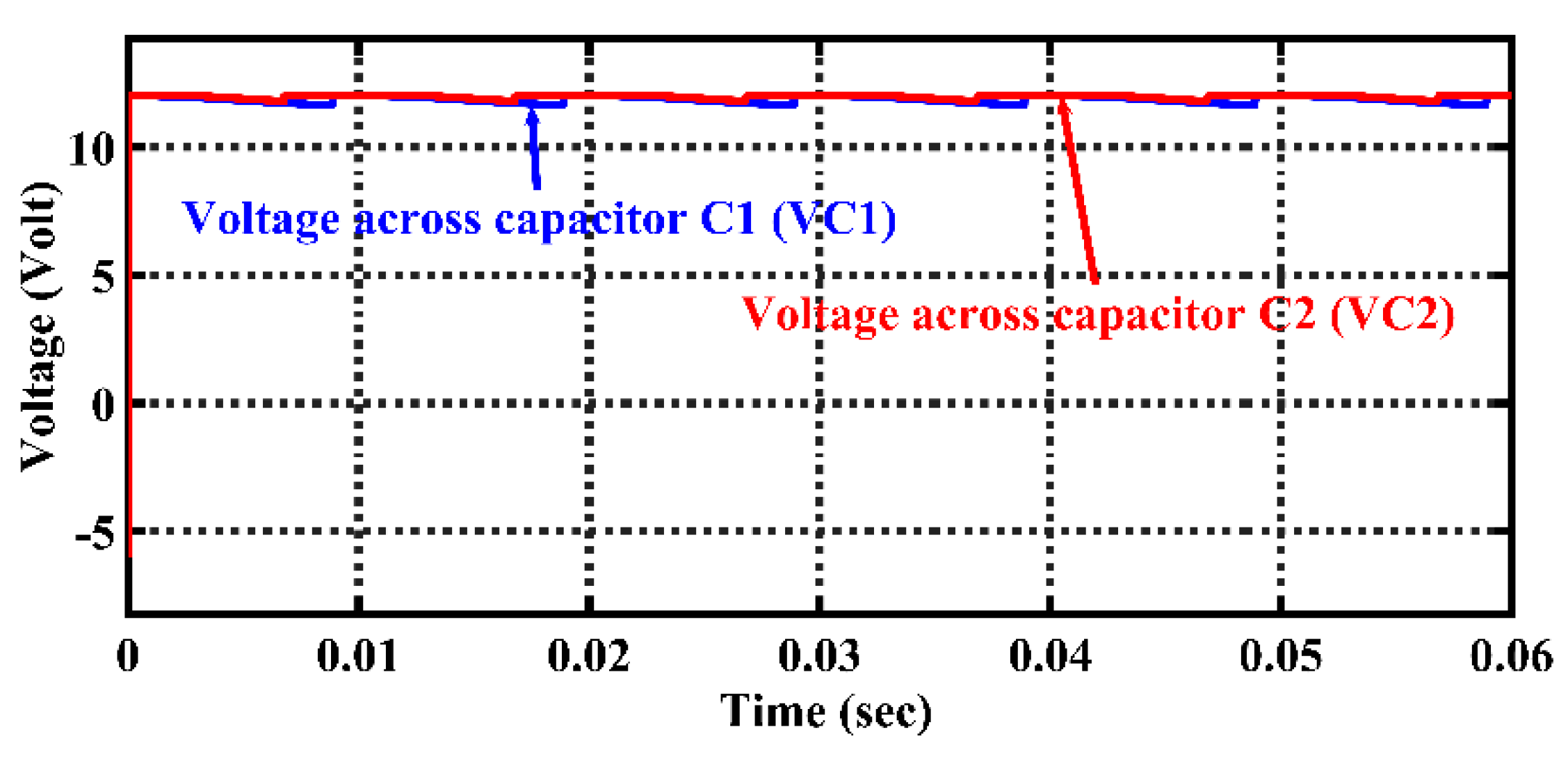
4.2. Capacitance Selection

The optimal value of capacitances for both switched capacitors (C1 and C2) is calculated based on the longest discharge time (LDT) over a complete cycle of the fundamental output voltage. The maximum quantity of charges from switched capacitors is discharged during LDT. Figure 4 shows the output voltage of this proposed topology (asymmetric) along with the LDT for both switched capacitors. The LDT for C2 is high compared to C1.
The amount of discharge during LDT for switched capacitor C2 can be calculated as
Q C 2 =   2 × t 6 T / 4 i 0 ( t ) d t
For resistive load, the output current during LDT can be expressed as
i 0 ( t )   =   6 V R L f o r   t 6 <   t   <   t 7 i 0 ( t )   =   7 V R L f o r   t 7 <   t   <   t 8
i 0 ( t )   =   8 V R L f o r   t 8 <   t   <   T / 4
Due to the application of a fundamental frequency scheme, the time t8, t7, and t6 can be given as
t 6 = S i n 1 ( 11 / 16 )   1   2 π f t 7 = S i n 1 ( 13 / 16 )     1 2 π f t 8 = S i n 1 ( 15 / 16 )     1 2 π f
From Equations (1)–(3), we get QC2 as
Q C 2   =   12 V 2 π f R L
The value of optimal capacitance for switched capacitor C2 can be calculated as
C 2 opt Q C 1   o r   Q C 2   p × V
From Equations (4) and (5),
C 2 opt   12 2 π f × R L × p
The amount of discharge during LDT for switched capacitor C1 can be calculated as
Q C 1 =   2 × t 8 T / 4 i 0 ( t ) d t
From Equations (2), (3), and (7), we get QC1 as
Q C   =   6 V 2 π f R L
From Equations (5) and (8), the optimal capacitance (C1opt) for switched capacitor C1 is given:
C 1 opt   6 2 π f × R L × p
where p is the maximum allowable output voltage ripple in percentage, RL is load resistance, and V is input source voltage. From Equations (6) and (9), it can be observed that the optimal value of capacitances depends on the ripple in voltage, load resistance, and operating frequency. The variation of the optimal capacitance C2opt with frequency (at RL = 100 Ω) for different values of voltage ripples are shown in Figure 5a. The variation in the optimal capacitances (C1opt and C2opt) with load resistance for different values of voltage ripples is shown in Figure 5b,d, respectively. From Figure 5b,d, it is clear that, for a particular value of voltage ripple, the values of optimal capacitances (C1opt and C2opt) decrease as the load resistance increases.
For R-L load, the output current can be expressed as
i 0 ( t ) = I 0 m a x s i n ( ω t φ )
where   φ is the phase angle between the fundamental output voltage and output current.
From Equations (1), (3), and (10), we get QC2 as
Q C 2   =   2 × t t 6 T / 4 I 0 m a x s i n ( ω t φ ) d t Q C 2 =   I 0 m a x 2 π f [ c o s   ( 0.75   φ )   s i n   ( φ ) ]
From Equations (5) and (11),
C 2 opt I 0 m a x 2 π f × V × p [ c o s   ( 0.75   φ )   s i n   ( φ ) ]
From Equations (3), (7), and (10), we get QC1 as
Q C 1   =   2 × t t 8 T / 4 I 0 m a x s i n ( ω t φ ) d t
Q C 1 =   I 0 m a x 2 π f [ c o s   ( 1.21   φ )   s i n   ( φ ) ]
From Equations (5) and (13), we get the optimal value of capacitance C1opt:
C 2 opt I 0 m a x 2 π f × V × p [ c o s   ( 1.21   φ )   s i n   ( φ ) ]
For plotting the graph between the optimal capacitance and phase angle for different values of voltage ripple, we take I0max = 4A and V = 20 volt. Figure 5c,e show the variation in optimal capacitances (C1opt and C2opt) with phase angle for different voltage ripples. From these figures, it is clear that, for a particular value of voltage ripple, the optimal capacitance decreases as the phase angle increases.

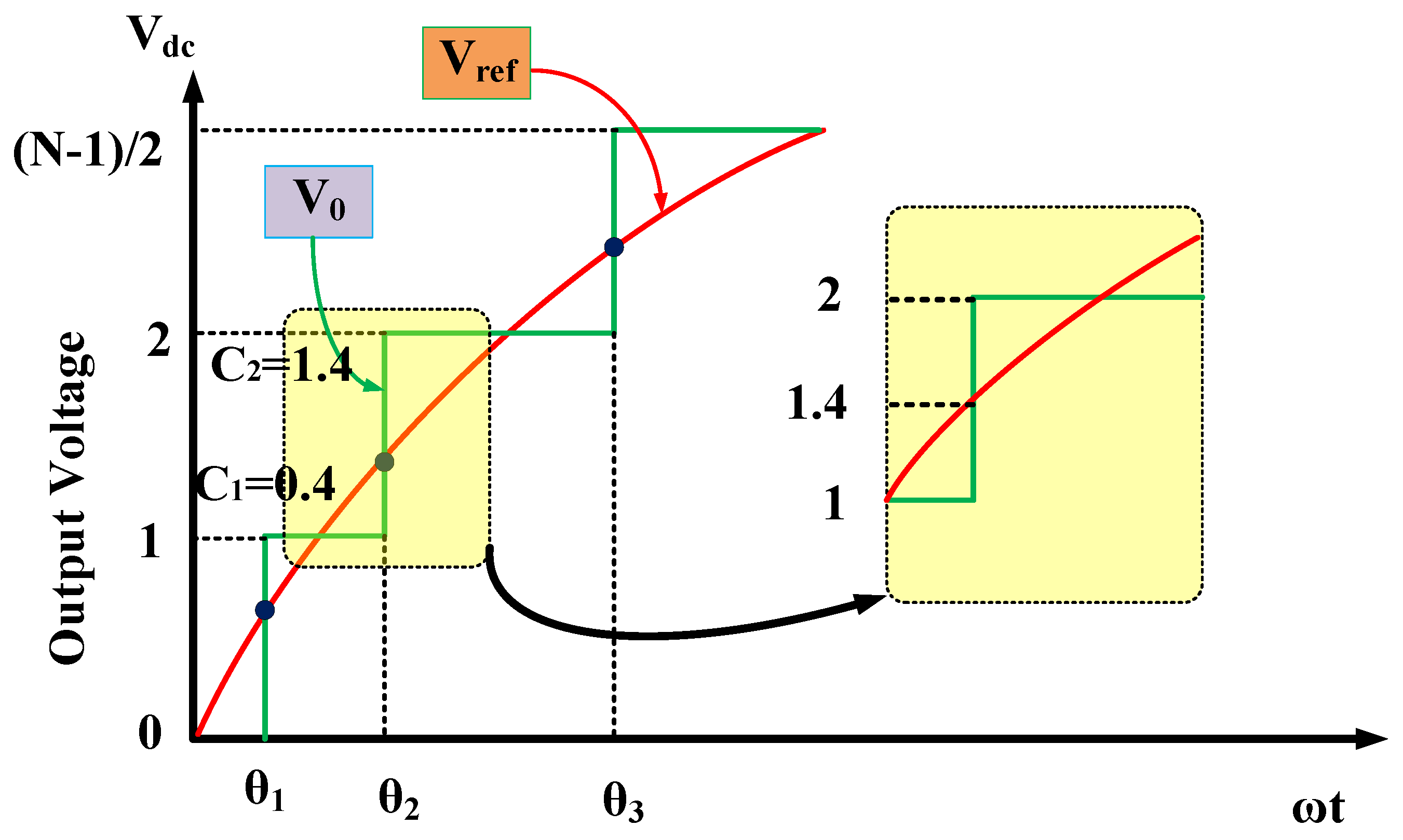
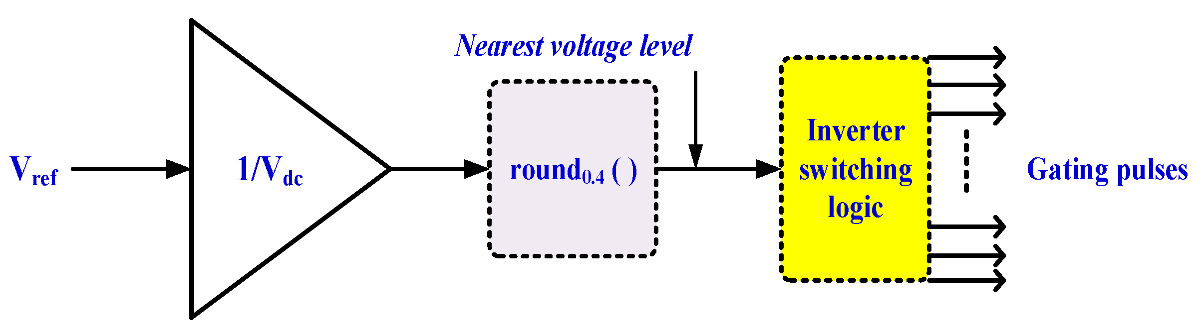
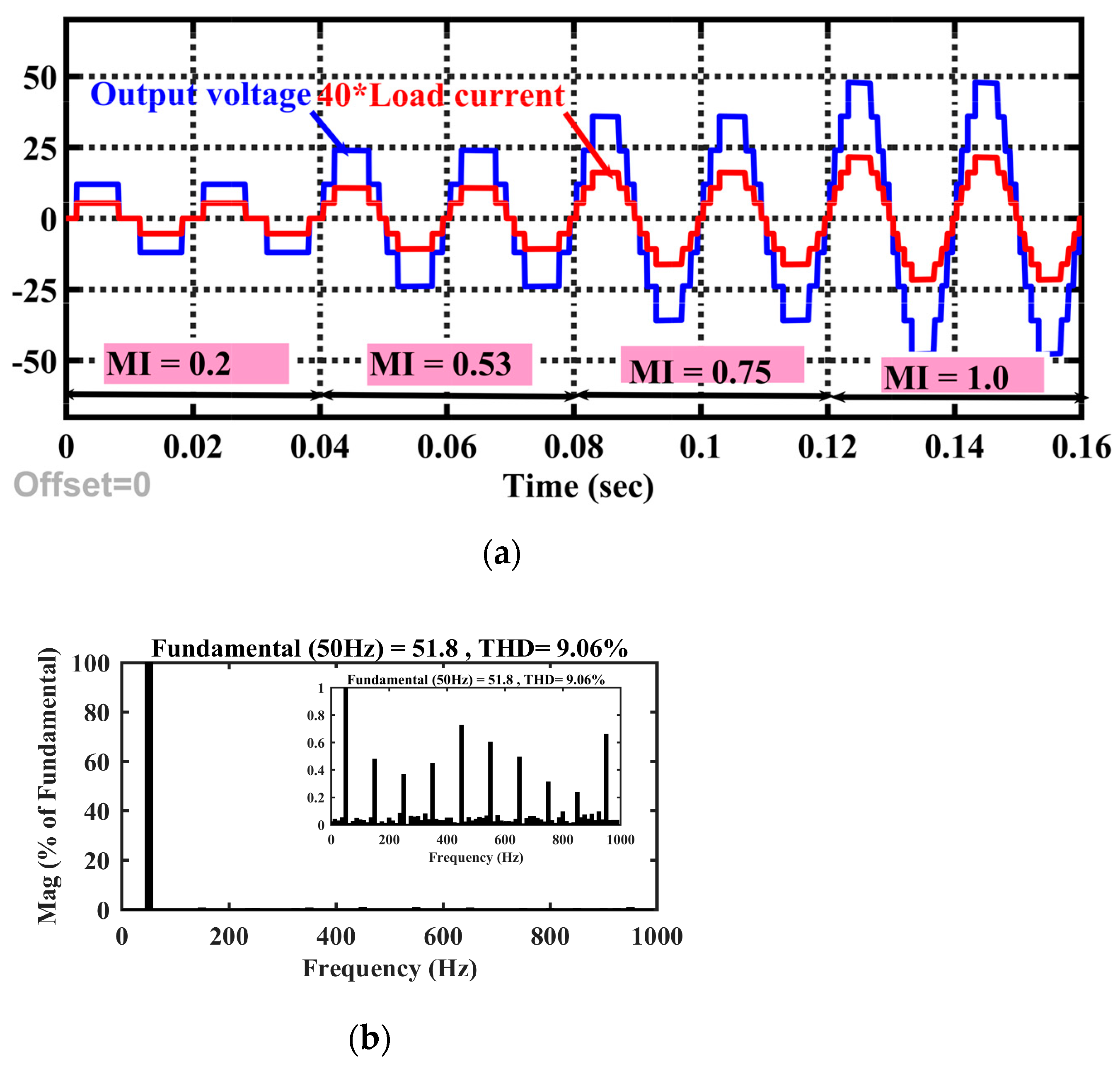
4.3. Modulation Scheme

Different modulation schemes are used for controlling the MLI output voltage. Apart from reducing THD, fundamental frequency switching schemes are also capable of minimizing the switching losses. Fundamental switching frequency schemes such as Selective Harmonic Elimination (SHE), nearest level control, and space vector control are preferred for high power applications. The main disadvantage of SHE is to solve the system of nonlinear trigonometric transcendental equations, which consume more computational time. Hence, the SHE technique is not concerned with real-time (closed-loop) applications. The nearest control techniques can eliminate this drawback of SHE. Nearest Level Control (NLC) can be classified as (1) the nearest space vector control and (2) nearest level control [26]. In this work, an optimized nearest level control is utilized for controlling the output voltage and different carrier signals are compared with a reference signal [26]. The level generation method and block scheme are shown in Figure 6 and Figure 7, respectively, for the NLC.
The equation for output voltage is shown below:
Vout = M * (Nlevel − 1)/2 * Vdc * cos (wt)
where m is the modulation index and is expressed as
M = Vref (max)/nVdc
where n = (Nlevel − 1)/2.

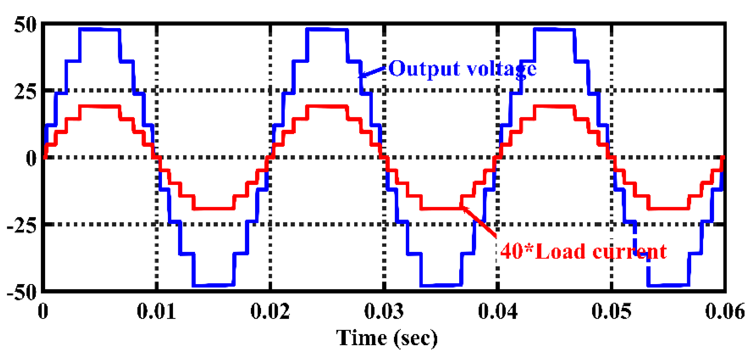
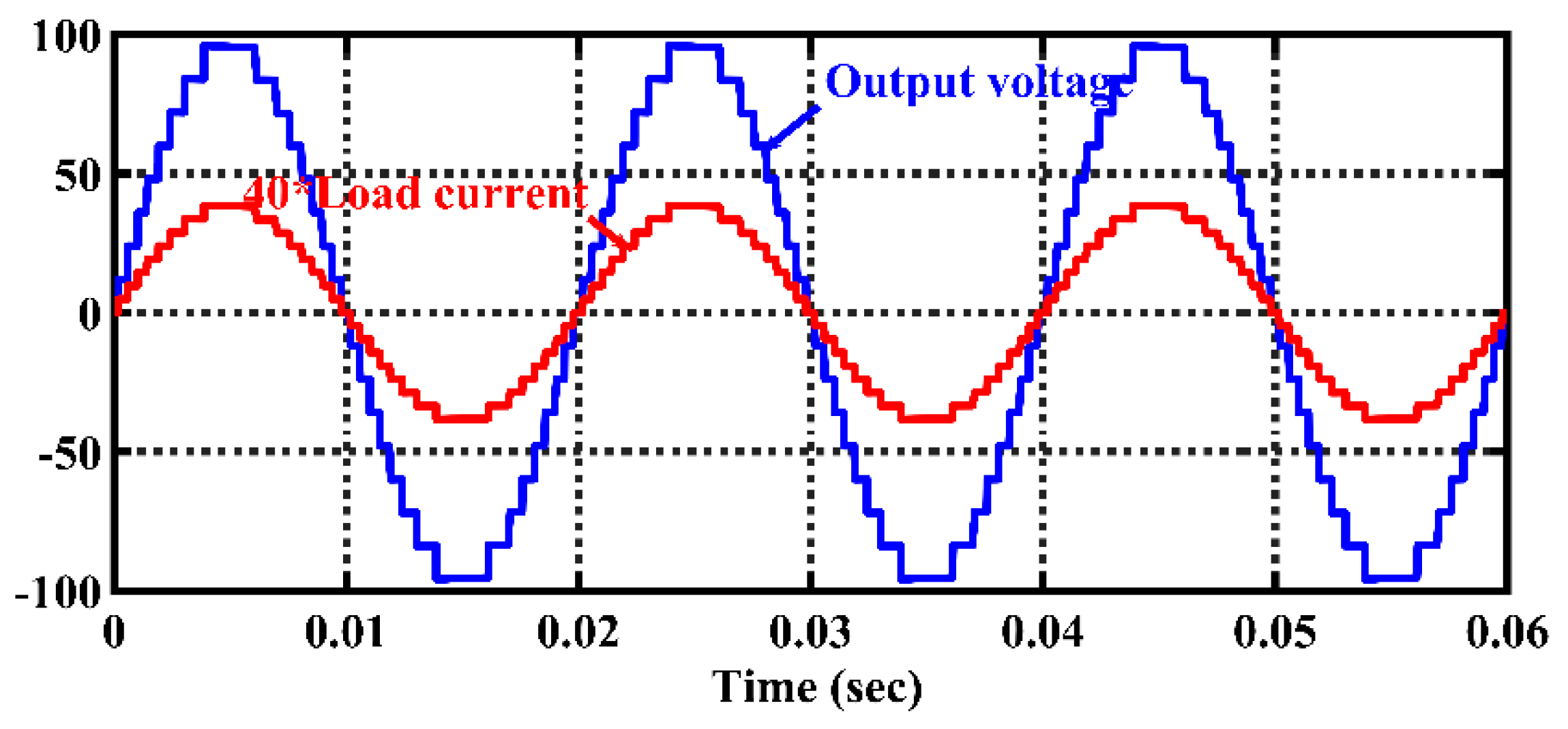
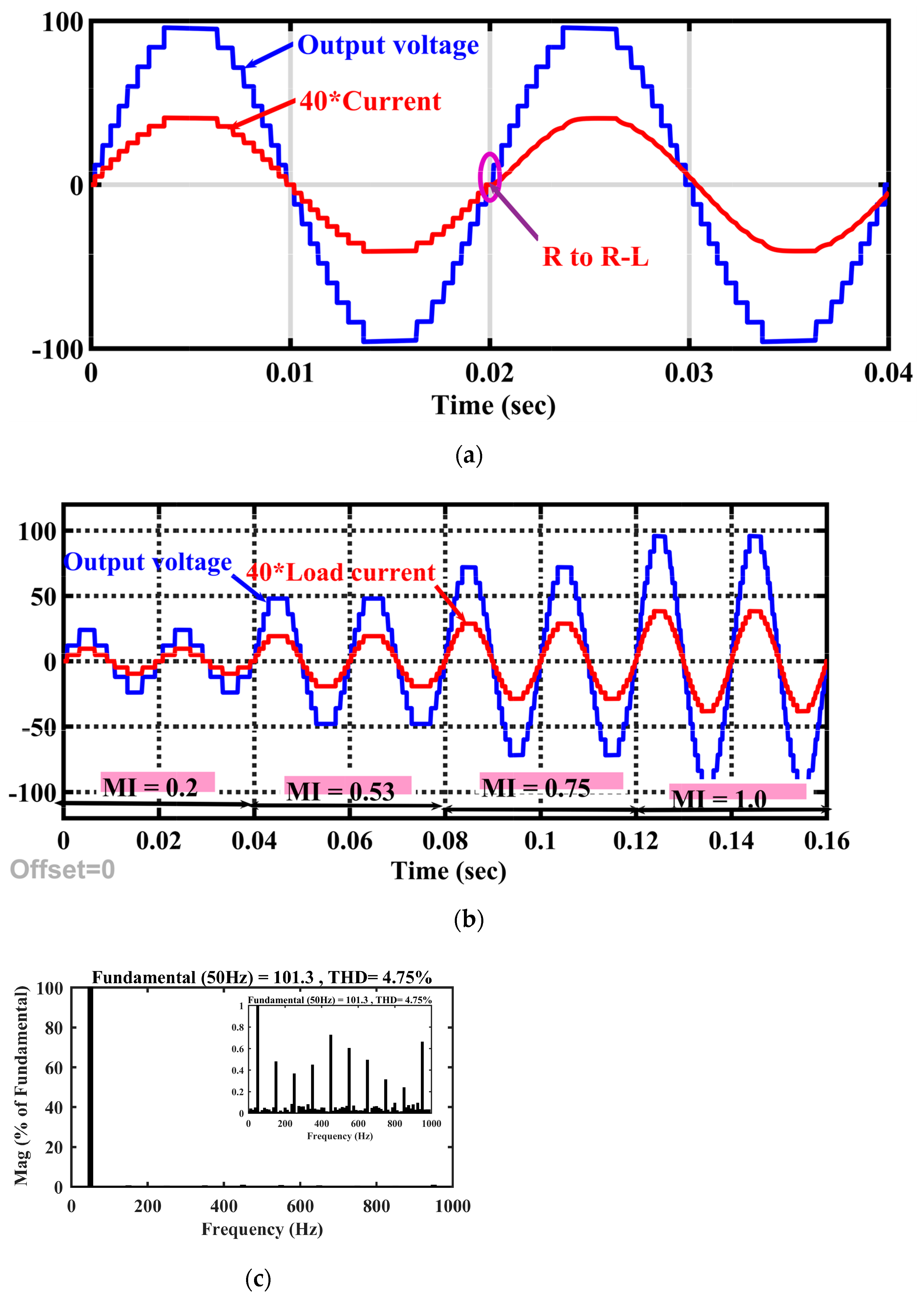
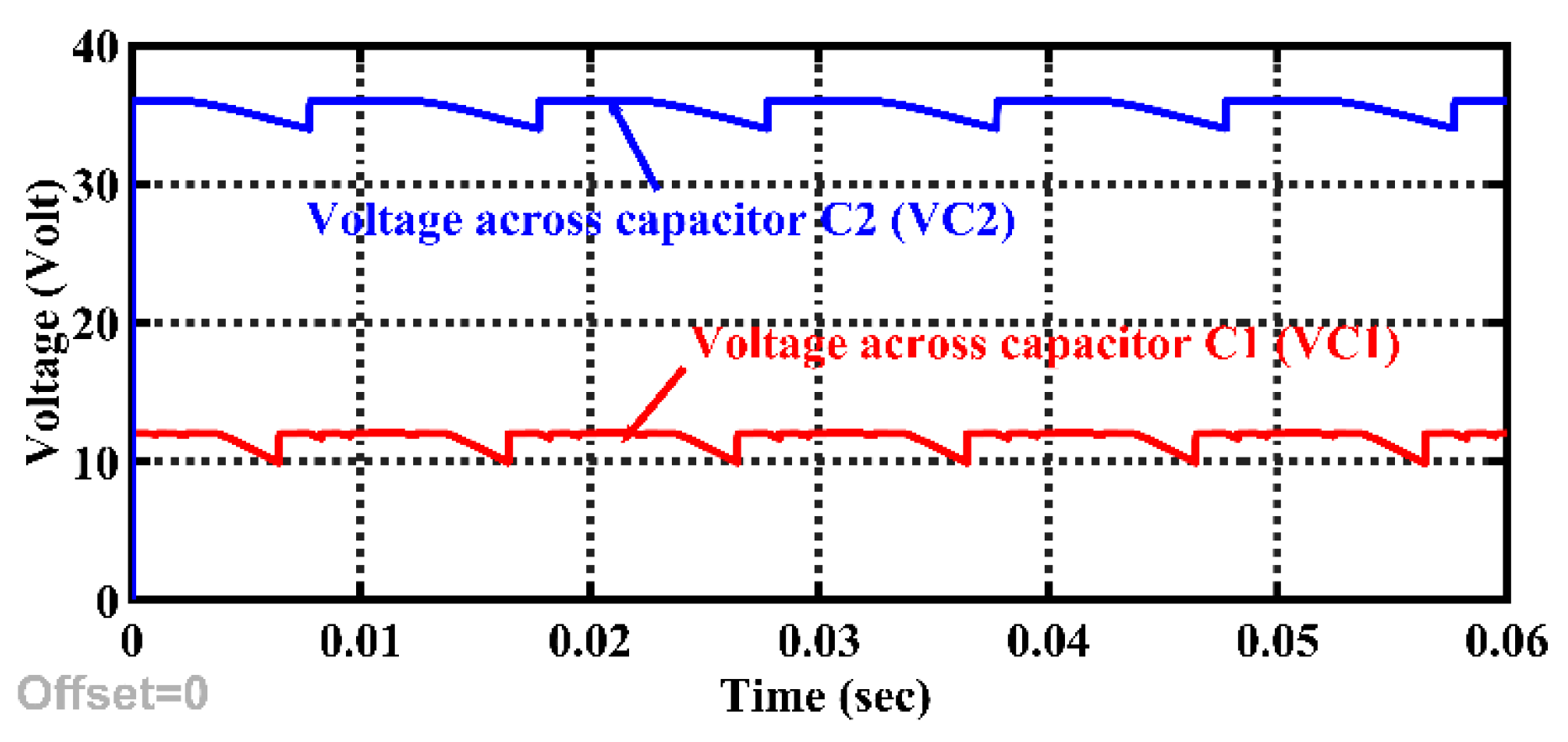
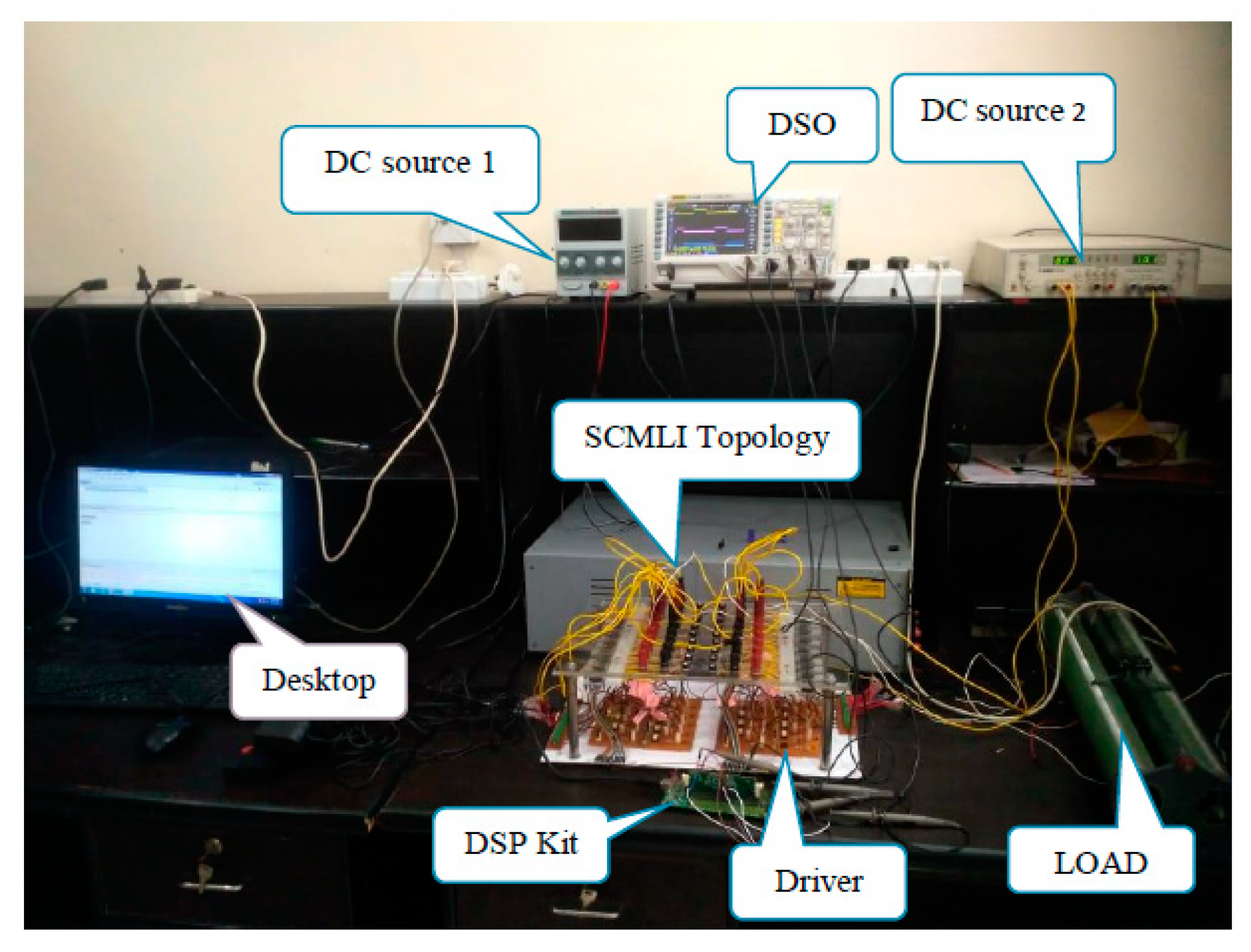
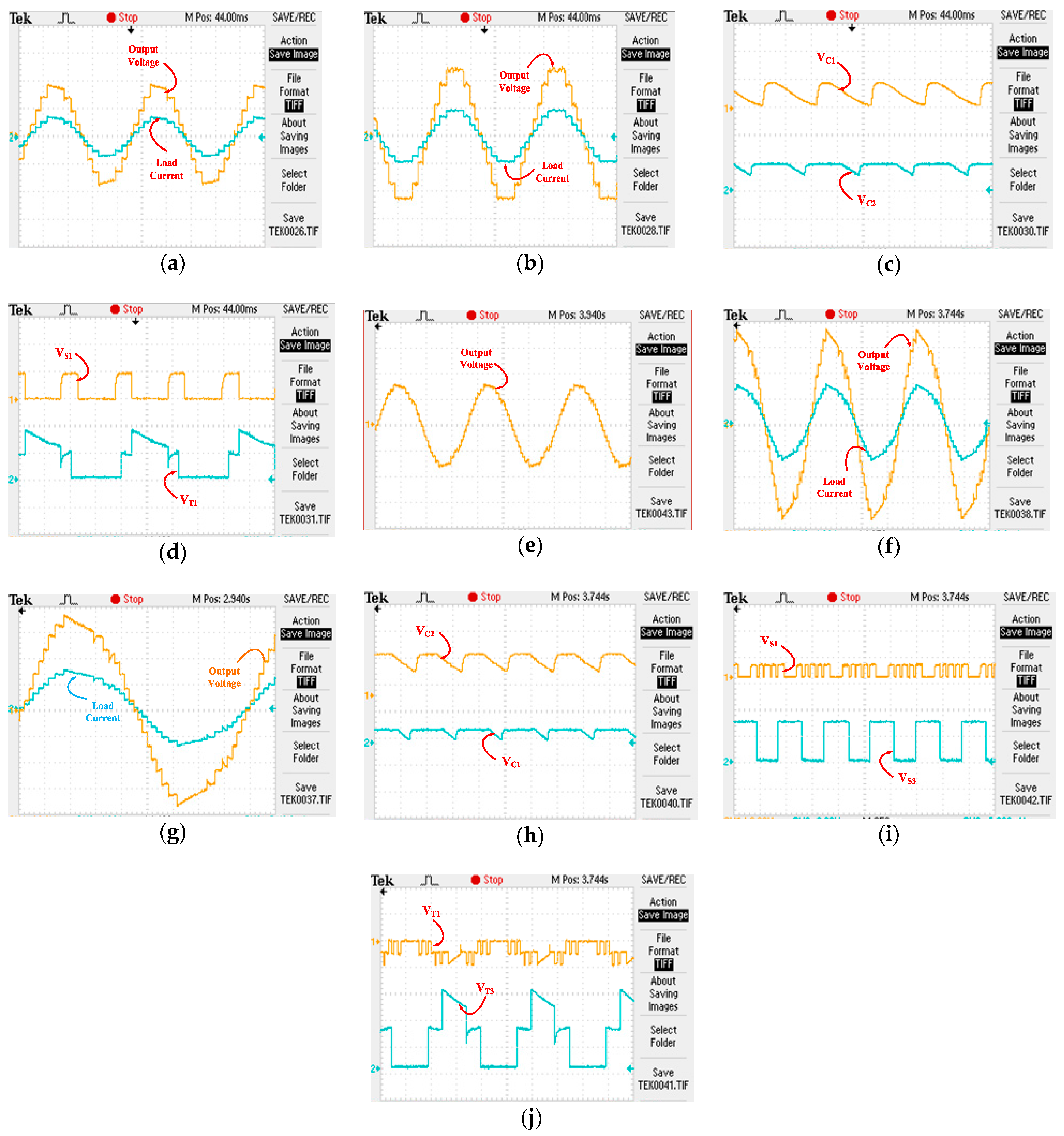
5. Simulation and Hardware Realization of the Basic Unit of the Proposed GSMLI Topologies

To assert the feasibility of the topologies, a MATLAB®/Simulink-based simulation was carried out. For the simulation of this topology in symmetric configuration, V1 and V2 were taken equal to 12 volts and the other parameters were taken according to Table 3. For simulation of the proposed topology in asymmetric configuration, V1 and V2 were taken equal to 12 and 36 volts, respectively, and the other parameters were taken according to Table 3.
Figure 8 shows the output voltage waveform and load current for the symmetric configuration (9 levels) of the proposed topology under R load for M at unity. Figure 9a shows the output voltage and current for dynamic change in modulation index and Figure 9b shows the total harmonics distortion (THD) in output voltage for symmetric configuration. Figure 10 show the voltage across capacitor C1 (2.5% ripple) and capacitor C2 (2.5% ripple) under the symmetric configuration. Figure 11 shows the waveforms of load current and output voltage for the asymmetric configuration (17 levels) of this topology at M = 1.0 with a purely resistive load. From these figures, it is confirmed that the proposed topology has the capability to generate all positive and negative voltage levels. A gain factor of 40 was taken to multiply the load current in order to have its scale be the same as that of the output voltage. While Figure 12a shows the voltage and current during dynamic change in the load from resistive to resistive-inductive, Figure 12b shows the voltage and current for the asymmetric case for a varying modulation index. THD in output voltage is 9.06% and 4.63% under the symmetric (9 levels) and asymmetric (17 levels) configurations, respectively. Due to the resistive load, the current harmonic spectrum is the same as the load voltage. Figure 13 show the voltage across capacitor C1 (2.5% ripple) and capacitor C2 (2.5% ripple) under the asymmetric configuration.
A laboratory prototype was developed in order to verify the simulation results and performance of the proposed SCMLI topology. Figure 14 shows the setup of the laboratory prototype for the proposed topology. In this experimental work, an Insulated Gate Bipolar Transistor (IGBT) (FGA25N120AND) with rating 1200 V/25 A was utilized as the power electronic switch signals to the switches by interfacing with SIMULINK.
Diode BEC0141 with a rating of 10A was used as the power diodes, an electrolyte capacitor with a rating of 4700 µF/63V was utilized as the switched capacitors, and TMS320F28335 (Texas Instruments) was used as a controller for the generation of the gating prototype and controller isolated by using the TLP 250 (TOSHIBA) optocoupler. A Digital Storage Oscilloscope (TPS2024B TEKTRONIX) was employed for the measurement of the waveforms of voltage and current. For the experimental results of the symmetric configuration, voltage sources V1 and V2 were taken equal to 12 volts each. This resulted in a 9-level staircase output voltage with a 48-volt peak value, as shown in Figure 15a. Figure 15a also shows the load current when a purely resistive load of 100 Ω was connected at the output. Figure 15b shows the waveform of output voltage and load current when the DC voltage sources were connected across capacitors C1 and C2 in the symmetric configuration. Figure 15c,d show the waveform of voltage across capacitors C1 and C2 and the waveform of the blocked voltage across switches S1 and T1, respectively, in the symmetric configuration. The peak values of voltage across capacitors C1 and C2 are 12 volts. The peak value of the blocked voltage across switches S1 and T1 are 12 and 24 volts, respectively, which verify the equations for maximum blocked voltage by switches. For the experimental results of asymmetric configuration, voltage sources V1 and V2 were taken 12 volts and 36 volts, respectively. This resulted in a 17-level staircase output voltage with a 96-volt peak value, as shown in Figure 15e under the no-load condition. Figure 15f shows the output voltage and load current waveform when a purely resistive load of 100 Ω was connected at the output. Figure 15g shows the waveform of output voltage (17 levels) and load current to observe the levels clearly. Figure 15h–j show the waveform of the voltage across capacitors C1 and C2, the waveform of blocked voltage across switches S1 and S3, and the waveform of blocked voltage across switches T1 and T3, respectively, in an asymmetric configuration. The peak values of voltage across capacitors C1 and C2 are 12 and 36 volts. The peak values of the blocked voltage across switches S1, S3, T1, and T3 are 12, 12, 24, and 72 volts, respectively, which verify the equations for maximum blocked voltage by switches. It is clear that the experimental results have a close agreement with the simulation results.

6. Conclusions

In this paper, a generalized structure for the MLI topology was presented. The generalized structures including various basic units and bidirectional switches, and a detailed analysis of this structure for two different methods depending on the selection of voltage sources are also presented. In the topology, capacitor voltages are self-balanced, due to which no voltage balancing algorithm is needed. The comparative study of the generalized structure was performed, and the results show superior performance under various performance parameters. The generalized structure needs less switches, capacitors, drivers, and TSV (in per unit) for a higher level of voltage output. Finally, to validate the performance, the simulation and experimental results were presented for symmetric (9-level voltage) and asymmetric (17-level voltage) configurations for a basic unit. The experimental results validate the performance obtained by simulation. The proposed modular structure is suitable for solar PV application. Moreover, the 9 levels can find application in electric vehicle driven applications. The number of DC power sources becomes higher for a higher level of operation. Future research should focus on the replacement of the DC power supplies with capacitors for a cost-effective solution for high power applications.

Author Contributions

Conceptualization, M.A.; data curation, A.S.; formal analysis, M.A., A.S., A.A. (Anzar Ahmad), and A.A. (Afroz Alam); funding acquisition, S.A., M.S., M.Z., and M.F.; investigation, M.A., A.S., A.A. (Anzar Ahmad), A.A. (Afroz Alam), S.A., M.S., M.Z., and M.F.; methodology, A.S., A.A. (Anzar Ahmad), A.A. (Afroz Alam), M.S., M.Z., and M.F.; project administration, A.S., S.A., M.S., and M.F.; supervision, A.S. and S.A.; writing—original draft, M.A. and A.S.; writing—review and editing, A.A. (Afroz Alam) and S.A. All authors have read and agreed to the published version of the manuscript.

Funding

The authors extend their appreciation to the Deanship of Scientific Research at King Saud University for funding this work through research group No (RG- 1438-089).

Institutional Review Board Statement

Not applicable.

Informed Consent Statement

Not applicable.

Data Availability Statement

Not applicable.

Conflicts of Interest

The authors declare no conflict of interest.

References

  1. Nabae, A.; Takahashi, I.; Akagi, H. A New Neutral-Point-Clamped PWM Inverter. IEEE Trans. Ind. Appl. 1981, 17, 518–523. [Google Scholar] [CrossRef]
  2. Gupta, K.K.; Ranjan, A.; Bhatnagar, P.; Sahu, L.K.; Jain, S. Multilevel inverter topologies with reduced device count: A review. IEEE Trans. Power Electron. 2016, 31, 135–151. [Google Scholar] [CrossRef]
  3. Alishah, R.S.; Sabahi, M.; Nazarpour, D.; Hosseini, S.H. Novel multilevel inverter topologies for medium and high-voltage applications with lower values of blocked voltage by switches. IET Power Electron. 2014, 7, 3062–3071. [Google Scholar] [CrossRef]
  4. Zhang, Y.; Adam, G.P.; Lim, T.C.; Finney, S.J.; Williams, B.W. Hybrid Multilevel Converter: Capacitor Voltage Balancing Limits and its Extension. IEEE Trans. Ind. Inform. 2013, 9, 2063–2073. [Google Scholar] [CrossRef]
  5. Abu-Rub, H.; Holtz, J.; Rodriguez, J.; Baoming, G. Medet alm-voltage multilevel converters; state of the art challenges and requirements in industrial applications. IEEE Trans. Ind. Electron. 2010, 57, 2581–2596. [Google Scholar] [CrossRef]
  6. Rodriguez, J.; Franquelo, L.G.; Kouro, S.; Leon, J.I.; Portillo, R.C.; Prats, M.A.M.; Perez, M.A. Multilevel converters: An enabling technology for high-power applications. Proc. IEEE 2009, 97, 1786–1817. [Google Scholar] [CrossRef] [Green Version]
  7. Roy, T.; Sadhu, P.K.; Dasgupta, A. Cross-Switched Multilevel Inverter Using Novel Switched Capacitor Converters. IEEE Trans. Ind. Electron. 2019, 66, 8521–8532. [Google Scholar] [CrossRef]
  8. Babaei, E.; Hosseini, S.H. New cascaded multilevel inverter topology with minimum number of switches. J. Energy Convers. Manag. 2009, 50, 2761–2767. [Google Scholar] [CrossRef]
  9. Kangarlu, M.F.; Babaei, E.; Laali, S. Symmetric multilevel inverter with reduced components based on non-insulated dc voltage sources. IET Power Electron. 2012, 5, 571–581. [Google Scholar] [CrossRef]
  10. Alishah, R.S.; Nazarpour, D.; Hosseini, S.H.; Sabahi, M. New hybrid structure for multilevel inverter with fewer number of components for high-voltage levels. IET Power Electron. 2014, 1, 96–104. [Google Scholar] [CrossRef]
  11. Siddique, M.D.; Saad, M.; Sarwar, A.; Alam, A.; Shah, N.M. Dual asymmetrical dc voltage source based switched capacitor boost multilevel inverter topology. IET Power Electron. 2020, 7, 1481–1486. [Google Scholar] [CrossRef]
  12. Waltrich, G.; Barbi, I. Three-phase cascaded multilevel inverter using power cells with two inverter legs in series. IEEE Trans. Ind. Electron. 2010, 57, 2605–2612. [Google Scholar] [CrossRef] [Green Version]
  13. Alishah, R.S.; Nazarpour, D.; Hosseini, S.H.; Sabahi, M. Reduction of power electronic elements in multilevel converters using a new cascade structure. IEEE Trans. Ind. Electron. 2015, 62, 256–269. [Google Scholar] [CrossRef]
  14. Babaei, E.; Laali, S.; Alilu, S. Cascaded multilevel inverter with series connection of novel H-bridge basic units. IEEE Trans. Ind. Electron. 2014, 61, 6664–6671. [Google Scholar] [CrossRef]
  15. Boora, K.; Kumar, J. General topology for asymmetrical multilevel inverter with reduced number of switches. IET Power Electron. 2017, 10, 2034–2041. [Google Scholar] [CrossRef]
  16. Banaei, M.R.; Salary, E. Verification of new family for cascade multilevel inverter switch reduction of components. J. Electr. Eng. Technol. 2011, 6, 245–254. [Google Scholar] [CrossRef] [Green Version]
  17. Banaei, M.R.; JannatiOskuee, M.R.; Khounjahan, H. Reconfiguration of semi-cascaded multilevel inverter to improve systems performance parameters. IET Power Electron. 2014, 7, 1106–1112. [Google Scholar] [CrossRef]
  18. Alishah, R.S.; Hosseini, S.H. Novel topologies for symmetric, asymmetric, and cascade switched-diode mutilevel converter with minimum number of power electronic components. IEEE Trans. Ind. Electron. 2014, 61, 5300–5310. [Google Scholar] [CrossRef]
  19. Hussan, M.R.; Sarwar, A.; Siddique, M.D.; Mekhilef, S.; Ahmad, S.; Sharaf, M.; Zaindin, M.; Firdausi, M. A Novel Switched-Capacitor Multilevel Inverter Topology for Energy Storage and Smart Grid Applications. Electronics 2020, 9, 1703. [Google Scholar] [CrossRef]
  20. Wang, L.; Wu, Q.H.; Tang, W. Novel Cascaded Switched-Diode Multilevel Inverter for Renewable Energy Integration. IEEE Trans. Energy Convers. 2017, 32, 1574–1582. [Google Scholar] [CrossRef]
  21. Abdullah, R.; Rahim, N.A.; Sheikh Raihan, S.R.; Ahmad, A.Z. Five-level diode-clamped inverter with three-level boost converter. IEEE Trans. Ind. Electron. 2014, 61, 5155–5163. [Google Scholar] [CrossRef] [Green Version]
  22. Khazraei, M.; Sepahvand, H.; Corzine, K.A.; Ferdowsi, M. Active capacitor voltage balancing in single-phase flying-capacitor multilevel power converters. IEEE Trans. Ind. Electron. 2012, 59, 769–778. [Google Scholar] [CrossRef]
  23. Shukla, A.; Ghosh, A.; Joshi, A. Control of dc capacitor voltages in diode-clamped multilevel inverter using bidirectional buck-boost choppers. IET Power Electron. 2012, 5, 1723–1732. [Google Scholar] [CrossRef]
  24. Mak, O.C.; Ioinovici, A. Switched-capacitor inverter with high power density and enhanced regulation capability. IEEE Trans. Circuits Syst. I Fundam. Theory Appl. 1998, 45, 336–347. [Google Scholar]
  25. Alishah, R.S.; Hosseini, S.H.; Babaei, E.; Sabahi, M. Optimal design of new cascaded switch-ladder multilevel inverter structure. IEEE Trans. Ind. Electron. 2017, 64, 2072–2080. [Google Scholar] [CrossRef]
  26. Siddique, M.D.; Mekhilef, S.; Shah, N.; Sarwar, A.; Iqbal, A.; Tayyab, M.; Ansary, M.K. Low Switching Frequency Based Asymmetrical Multilevel Inverter Topology with Reduced Switch Count. IEEE Access 2019, 7, 86374–86383. [Google Scholar] [CrossRef]
  27. Lee, S.S.; Lee, K.; Alsofyani, I.M.; Bak, Y.; Wong, J.F. Improved Switched-Capacitor Integrated Multilevel Inverter with a DC Source String. IEEE Trans. Ind. Appl. 2019, 55, 7368–7376. [Google Scholar] [CrossRef]
  28. Siddique, M.D.; Mekhilef, S.; Shah, N.M.; Sarwar, A.; Memon, M.A. A New Single-Cascaded Multilevel Inverter Topology with Reduced Number of Switches and Voltage Stress. Int. Trans. Electr. Energy Syst. 2019. [Google Scholar] [CrossRef]
  29. Hosseini, S.H.; Alishah, R.S.; Gharehkoushan, A.Z. Enhancement of extracted maximum power from partially shaded multi-string PV panels using a new cascaded high step-up DC-DC-AC converter. In Proceedings of the 9th International Conference on Electrical and Electronics Engineering (ELECO 2015), Bursa, Turkey, 26–28 November 2015; pp. 644–648. [Google Scholar]
  30. Taghvaie, A.; Adabi, J.; Rezanejad, M. A Self-Balanced Step-Up Multilevel Inverter Based on Switched-Capacitor Structure. IEEE Trans. Power Electron. 2018, 33, 199–209. [Google Scholar] [CrossRef]
  31. Liu, J.; Zhu, X.; Zeng, J. A Seven-level Inverter with Self-balancing and Low Voltage Stress. IEEE J. Emerg. Sel. Top. Power Electron. 2018, 8, 685–696. [Google Scholar] [CrossRef]
Figure 1. Circuit diagram of the Generalized Structure of the Multilevel Inverter (GSMLI).
Applsci 11 01319 g001
Figure 2. Comparison curves: (a) number of switches vs. number of levels, (b) number of switches vs. number of levels, (c) number of switches vs. number of levels, and (d) total standing voltage (TSV) (per unit) vs. the number of levels.
Applsci 11 01319 g002
Figure 3. Conducting path for positive half-cycle modes.
Applsci 11 01319 g003aApplsci 11 01319 g003b
Figure 4. Waveform of output voltage (inverted negative half-cycle) along with the longest discharge time (LDT) of capacitors in asymmetric configuration.
Applsci 11 01319 g004
Figure 5. Variation in optimal capacitance C2opt with (a) frequency (f), (b) load resistance (RL), (c) and phase angle for different values of ripple in capacitor voltage and variation in optimal capacitance C1opt with (d) load resistance (RL) and (e) phase angle for different values of ripple in a capacitor voltage.
Applsci 11 01319 g005
Figure 6. Level generation method of the optimized nearest level control.
Applsci 11 01319 g006
Figure 7. Block diagram of an Optimized Nearest Level Control (ONLC).
Applsci 11 01319 g007
Figure 8. Output voltage and load current for symmetric configuration.
Applsci 11 01319 g008
Figure 9. (a) Output voltage and current for dynamic change in modulation index and (b) total harmonics distortion (THD) in output voltage for symmetric configuration.
Applsci 11 01319 g009
Figure 10. Voltage across capacitors C1 and C2 for symmetric configuration.
Applsci 11 01319 g010
Figure 11. Output voltage and load current for asymmetric configuration.
Applsci 11 01319 g011
Figure 12. (a) Output voltage and current for change in load from resistive to resistive-inductive, (b) output voltage and current for dynamic change in modulation index, and (c) THD in output voltage for asymmetric configuration.
Applsci 11 01319 g012
Figure 13. Voltage across capacitors C1 and C2 for asymmetric configuration.
Applsci 11 01319 g013
Figure 14. Experimental setup.
Applsci 11 01319 g014
Figure 15. Waveform of (a) output voltage (25 V/div) and load current (1.5 A/div). (b) Output voltage (20 V/div) and load current (0.5 A/div) when the voltage supply of 12 V was connected across both capacitors. (c) Voltage across capacitors C1 and C2 (12 V/div). (d) Blocked voltage across switches S1 and T1 (12 V/div) in symmetric configuration. Waveform of (e) output voltage (60 V/div) under the no-load condition. (f) Output voltage (20 V/div) and load current (0.75 A/div). (g) Output voltage (20 V/div) and load current (0.75 A/div) for showing one complete cycle (h). Voltage across capacitors C1 and C2 (25 V/div). (i) Blocked voltage across switches S1 and S3 (25 V/div). (j) Blocked voltage across switches T1 and T3 (24 V/div) in asymmetric configuration.
Applsci 11 01319 g015
Table 1. Generalized formulas for different devices of GSMLI.
Parametersn is the Number of StagesNL is the Number of Levels
First MethodSecond MethodFirst MethodSecond Method
NL8 n 2 + 8n + 1 2 2 n + 3   2 n + 3 + 1NLNL
Nsw8n + 28n + 22[−3+ 2 ( N L + 1 )]8log2[2 + 2 ( N L + 1 )] − 14
Ndri6n + 46n + 4[−2 + 3 2 2 ( N L + 1 )]6log2[2 + 2 ( N L + 1 )] − 8
Ndiode2n2n[−2 + 1 2 2 ( N L + 1 )]2log2[2 + 2 ( N L + 1 )] − 4
Ncap2n2n[−2 + 1 2 2 ( N L + 1 )]2log2[2 + 2 ( N L + 1 )] − 4
Table 2. States of switches and capacitors.
StatesOutput Voltage(V0) S 1   or     S 2 ¯ S 3   or   S 4 ¯ T 1   or     T 2 ¯ T 3   or     T 4 ¯ T 5   or     T 6 ¯ T 7   or     T 8 ¯ C1C2(V0)
Symmetric (V1 = V2 = VC1 = VC2 = V)
(V0)
Asymmetric (V1 = VC1 = V & V2 = VC2 = 3V)
A0V000000cc0V0V
BV1001000--V1 = VV1 = V
CV1 + VC1101000d-V1 + VC1 = 2VV1 + VC1 = 2V
DV2000010c-V2 = VV2 = 3V
EV1 + V2001010--V1 + V2 = 2VV1 + V2 = 4V
FV1 + VC1 + V2101010d-V1 + VC1 + V2 = 3VV1 + VC1 + V2 = 5V
GV2 + VC2010010cdV2 + VC2 = 2VV2 + VC2 = 6V
HV1 + V2 + VC2011010-dV1 + V2 + VC2 = 3VV1 + V2 + VC2 = 7V
IV1 + VC1 + V2 + VC2111010ddV1 + VC1 + V2 + VC2= 4VV1 + VC1 + V2 + VC2= 8V
JV1000100ccV1 = −VV1 = −V
K−(V1 + VC1)100100d-−(V1 + VC1) = −2V−(V1 + VC1) = −2V
LV2000001c-V2 = −VV2 = −3V
M−(V1 + V2)000101--−(V1 + V2) = −2V−(V1 + V2) = −4V
N−(V1 + VC1 + V2)100101d-−(V1 + VC1 + V2) = −3V−(V1 + VC1 + V2) = −5V
O−(V2 + VC2)010001cd−(V2 + VC2) = −2V−(V2 + VC2) = −6V
P−(V1 + V2 + VC2)010101-d−(V1 + V2 + VC2) = −3V−(V1 + V2 + VC2) = −7V
Q−(V1 + VC1 + V2 + VC2)110101dd−(V1 + VC1 + V2 + VC2) = −4V−(V1 + VC1 + V2 + VC2) = −8V
Table 3. Parameters used in the simulation of the symmetrical and asymmetrical configurations.
Parameters Attributes
Switches (T1 to S4)IGBT/Diode
Switching frequency (fs)50 Hz
Load (purely resistive)100 Ω,
Capacitors C1,C22200 µF, 4300 µF
Publisher’s Note: MDPI stays neutral with regard to jurisdictional claims in published maps and institutional affiliations.

